US7636101B2 - MEMS scanner adapted to a laser printer - Google Patents
MEMS scanner adapted to a laser printer Download PDFInfo
- Publication number
- US7636101B2 US7636101B2 US11/502,131 US50213106A US7636101B2 US 7636101 B2 US7636101 B2 US 7636101B2 US 50213106 A US50213106 A US 50213106A US 7636101 B2 US7636101 B2 US 7636101B2
- Authority
- US
- United States
- Prior art keywords
- mems scanner
- laser printer
- scan plate
- torsion arms
- scan
- Prior art date
- Legal status (The legal status is an assumption and is not a legal conclusion. Google has not performed a legal analysis and makes no representation as to the accuracy of the status listed.)
- Expired - Fee Related, expires
Links
Images


Classifications
-
- G—PHYSICS
- G02—OPTICS
- G02B—OPTICAL ELEMENTS, SYSTEMS OR APPARATUS
- G02B26/00—Optical devices or arrangements for the control of light using movable or deformable optical elements
- G02B26/08—Optical devices or arrangements for the control of light using movable or deformable optical elements for controlling the direction of light
- G02B26/0816—Optical devices or arrangements for the control of light using movable or deformable optical elements for controlling the direction of light by means of one or more reflecting elements
- G02B26/0833—Optical devices or arrangements for the control of light using movable or deformable optical elements for controlling the direction of light by means of one or more reflecting elements the reflecting element being a micromechanical device, e.g. a MEMS mirror, DMD
- G02B26/0858—Optical devices or arrangements for the control of light using movable or deformable optical elements for controlling the direction of light by means of one or more reflecting elements the reflecting element being a micromechanical device, e.g. a MEMS mirror, DMD the reflecting means being moved or deformed by piezoelectric means
-
- B—PERFORMING OPERATIONS; TRANSPORTING
- B41—PRINTING; LINING MACHINES; TYPEWRITERS; STAMPS
- B41J—TYPEWRITERS; SELECTIVE PRINTING MECHANISMS, i.e. MECHANISMS PRINTING OTHERWISE THAN FROM A FORME; CORRECTION OF TYPOGRAPHICAL ERRORS
- B41J2/00—Typewriters or selective printing mechanisms characterised by the printing or marking process for which they are designed
- B41J2/435—Typewriters or selective printing mechanisms characterised by the printing or marking process for which they are designed characterised by selective application of radiation to a printing material or impression-transfer material
- B41J2/47—Typewriters or selective printing mechanisms characterised by the printing or marking process for which they are designed characterised by selective application of radiation to a printing material or impression-transfer material using the combination of scanning and modulation of light
- B41J2/471—Typewriters or selective printing mechanisms characterised by the printing or marking process for which they are designed characterised by selective application of radiation to a printing material or impression-transfer material using the combination of scanning and modulation of light using dot sequential main scanning by means of a light deflector, e.g. a rotating polygonal mirror
-
- G—PHYSICS
- G02—OPTICS
- G02B—OPTICAL ELEMENTS, SYSTEMS OR APPARATUS
- G02B26/00—Optical devices or arrangements for the control of light using movable or deformable optical elements
- G02B26/08—Optical devices or arrangements for the control of light using movable or deformable optical elements for controlling the direction of light
- G02B26/0816—Optical devices or arrangements for the control of light using movable or deformable optical elements for controlling the direction of light by means of one or more reflecting elements
- G02B26/0833—Optical devices or arrangements for the control of light using movable or deformable optical elements for controlling the direction of light by means of one or more reflecting elements the reflecting element being a micromechanical device, e.g. a MEMS mirror, DMD
- G02B26/0841—Optical devices or arrangements for the control of light using movable or deformable optical elements for controlling the direction of light by means of one or more reflecting elements the reflecting element being a micromechanical device, e.g. a MEMS mirror, DMD the reflecting element being moved or deformed by electrostatic means
Definitions
- Electrophotographic, computer controlled printers have become pervasive in the office, factory, print shop, copy center, and home.
- An electrophotographic printer operates by transferring toner to plain paper and fusing the toner by means of heat, pressure, and/or other fixing technologies.
- the pattern of the transferred toner may form characters, graphic images, etc.
- electrophotography refers to the use of modulated light, frequently a scanned laser beam, to create an electrostatic latent image on a photoconductive carrying medium such as a drum or belt.
- the latent electrostatic image is formed by momentary electrical conductivity of the photoconductor in response to exposure to the modulated light.
- the momentary conductivity allows a surface charge to discharge through the photoconductor to a conductor held at a bias voltage at locations corresponding to the modulated light exposure.
- FIG. 1 is a diagram illustrating the principal features of an electrophotographic printer.
- a photoconductive drum 102 is rotated past a charging or sensitization station 104 that deposits a static charge substantially uniformly over the surface of the drum 102 .
- An imaging module 106 modulates light selectively over the surface of the photoconductor 102 . This causes the static charge in those spots receiving light to discharge through the photoconductive layer to a conductive layer on the backside of the photoconductor surface.
- the pattern of discharged and non-discharged spots is referred to as a latent electrostatic image or latent image.
- the photoconductor 102 is further rotated to a developer 108 , where oppositely charged toner, most often in the form of fine, dry particles, is attracted to and deposited on the surface of the photoconductor in a pattern corresponding to the latent image.
- the photoconductor 102 is further rotated to a transfer point, where the patterned toner is then transferred to the paper 112 , often using an electrostatic attraction element 110 such as a corona wire in the form of a corotron or scorotron.
- the photoconductive medium 102 is rotated past a discharge lamp 116 and a cleaner 118 , and then repeats the process as it is rotated to the sensitizer or charger 104 .
- LED light emitting diode
- LCD liquid crystal shutter
- vacuum fluorescent vacuum fluorescent
- other types of arrayed light modulator write heads have been used for modulating light onto the photoconductor.
- scanned laser beam exposure or imaging modules have gained favor in the art due to an appropriate balance of cost, speed, performance, and durability.
- An electrophotographic printer that uses a scanned laser beam to provide light modulation onto the surface of the photoconductive medium may be conveniently referred to as a laser beam printer or LBP.
- FIG. 2 illustrates the general construction of an LBP exposure unit 106 made according to the prior art with a rotating polygon beam scanner.
- a laser diode 202 having a wavelength matched to the sensitivity of the photoconductor (often infrared in the case of an organic photoconductor) is modulated with an image signal.
- Beam-forming optics 204 produce a laser beam having a desired shape and trajectory.
- the laser beam is reflected off a rotating polygon mirror 206 and is scanned across the photoconductor 102 through optical elements 208 .
- the design of the exposure module 106 is such that the reflective facets 210 a , 210 b , etc. of the rotating polygon 206 are placed forward of the center of rotation such that the arriving beam sweeps over each mirror surface as it is deflected across its deflection angle, the deflection angle being sufficient to traverse the photoconductor 102 .
- Rotating polygon mirrors may suffer from relatively large mass, slow ramp-up to speed, large size, noise, bearing reliability issues, relatively high power consumption, and other shortcomings.
- MEMS microelectromechanical system
- FIG. 2 is a diagrammatic view of a LBP exposure unit with a rotating polygon scanner made according to the prior art.
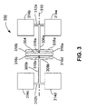
- FIG. 3 is a view of a MEMS scanner made according to an embodiment of the present invention.
- FIG. 4 is a graph illustrating the dynamic response of the MEMS scanner of FIG. 3 .
- FIG. 6 is a view of a mounting clamp for mounting the MEMS scanner of FIG. 3 .
- FIG. 7 is a detailed view of a piezo-electric stack used to form the actuator of FIG. 6 .
- FIG. 8 is a front perspective view of a MEMS scanner package for use in a LBP.
- FIG. 9 includes two additional perspective views of the MEMS scanner package of FIG. 8 .
- FIG. 3 illustrates a MEMS scanner 302 that may be used in a LBP.
- the exemplary embodiment shown herein relates to a 40 page per minute (ppm), 1200 dot per inch (dpi) LBP.
- MEMS scanner 302 is photolithographically formed from single-crystal silicon using bulk micromachining as is known to the art.
- a scan plate 304 having a mirror surface is coupled to a pair of torsion arms 306 a , 306 b through respective suspension beams 308 a , 308 b .
- Torsion arms 306 a , 306 b define a rotational axis 310 about which scan plate 304 and suspension beams 308 a , 308 b rotate.
- Suspension beams 308 a and 308 b help to keep the mirror surface relatively flat, typically within lambda/4, by spreading the torque loads induced by the torsion arms 306 a , 306 b across the surface of the scan plate 304 .
- Suspension beams 308 are coupled to scan plate 304 by respective outer (lateral) connectors 316 a , 316 b , 316 c , 316 d and respective axial connectors 318 a , 318 b .
- suspension elements 308 a , 316 a , 316 b , and 318 a form a first suspension coupling between first torsion arm 306 a and scan plate 304 .
- suspension elements 308 b , 316 c , 316 d , and 318 b form a second suspension coupling between second torsion arm 306 b and scan plate 304 .
- a mirror surface can be formed on the surface of scan plate 304 using metal, stacked dielectric, or other technologies known to the art.
- Aluminum can be used to form a mirror having greater than about 85% reflectivity at red and infrared wavelengths (having a local minimum at about 825 nanometers wavelength).
- Gold or silver can be used to form a mirror having greater than about 90% to 95% reflectivity at red and infrared wavelengths.
- Stacked (such as quarter-wave) dielectric reflectors can achieve very high reflectivity across a wide range of wavelengths.
- Torsion arms 306 a , 306 b terminate at respective “T-bars” 312 a and 312 b .
- T-bars 312 a and 312 b connect to respective mounting pads 314 a , 314 b and 314 c , 314 d as illustrated.
- T-bar 312 a and mounting pads 314 a , 314 b constitute a first mounting structure for coupling torsion arm 306 a to a support structure (not shown).
- T-bar 312 b and mounting pads 314 c , 314 d form a second mounting structure for coupling torsion arm 306 b to a support structure (not shown).
- mounting structures can take other forms, including for example a pair of rectangular mounting pads, each joined directly to a respective torsion arm, or other forms.
- a frame-type mounting structure may be formed peripheral to the scan plate 304 and torsion arms 306 a , 306 b .
- the exemplary embodiment of FIG. 3 may have certain advantages such as, for example, packing more devices per wafer, having reduced dynamic stress, allowing individual mounting pads to be coupled to actuators, and allowing the mounting pads 314 to “float” relative to one another, thereby reducing residual stresses in the MEMS scanner.
- Scan plate 304 is formed to be approximately 8 millimeters long (in the direction perpendicular to the axis of rotation 310 ) and 750 micrometers wide (in the direction parallel to the axis of rotation 310 ).
- the scan plate (and mirror formed thereon) has a lateral dimension about 10.67 times its longitudinal dimension.
- the mirror When driven with an appropriate signal, (such as a 5 kilohertz (KHz) sine wave varying between about 0 (zero) and 25-30 volts for a four actuator design) the mirror responds with a ⁇ 20° mechanical scan angle at a frequency of 5 KHz.
- KHz 5 kilohertz
- the torsion arms are etched to a full wafer thickness of 700 microns using DRIE processing.
- the width, depth, and length of the torsion arms and T-bars may be adjusted to produce alternative resonant scan frequencies and angles.
- the suspension beams 308 a , 308 b are 396 microns wide, are slightly bent to make a slightly obtuse angle with respective torsion arms 306 a , 306 b of 91.6 degrees, and extend laterally to an extent equal to the lateral extent of the 8 millimeter lateral dimension scan plate 304 .
- Respective suspension center connectors 318 a , 318 b extend from the centerlines of suspension beams 308 a , 308 b to the centerline of the scan plate 304 , a distance of 500 microns (including fillets).
- the center connectors 318 a , 318 b are each 164 microns wide and include 100 micron radius fillets at both ends.
- suspension outer connectors 316 a , 316 b , 316 c , and 316 d extend from the ends of suspension beams 308 a , 308 b to the scan plate 304 , one on each end of each suspension beam as indicated.
- the outer connectors 316 a , 316 b , 316 c , 316 d are each 250 microns wide (laterally) by 400 microns long (longitudinally) and do not have fillets.
- the respective suspensions thus each include a suspension beam 308 , a center suspension connector 318 , and two outer suspension connectors 316 ; and connect the torsion arms 306 a , 306 b to the scan plate 304 in a manner that reduces stress concentrations, spreads the torque load, and reduces dynamic deformation of the scan plate during operation.
- Alternative suspension configurations are possible and could be implemented by one skilled in the art.
- the T-bars 312 a , 312 b are each 1.8 millimeters long (total lateral dimension inclusive of fillets) by 400 microns wide (longitudinal dimension) and extend symmetrically from and perpendicular to the axis formed by torsion arms 306 a , 306 b .
- the outer ends of T-bars 312 a , 312 b connect to four respective mounting pads 314 a , 314 b , 314 c , 314 d with 200 micron radius fillets as shown.
- the mounting pads are each 5 millimeters square. The geometry of the T-bars and mounting pads may be adjusted to suit application requirements.
- FIG. 4 shows graphs illustrating the dynamic response of the MEMS scanner of FIG. 3 when a periodic drive signal is applied.
- Curve 402 indicates an amplitude response 404 as a function of periodic drive frequency 406 .
- Curve 408 illustrates scanner vs. drive phase 410 plotted against the same periodic drive frequency axis 406 . From inspection of curve 402 , one can see a peak in response at about 5 KHz corresponding to the resonance frequency of the MEMS scanner in the rotation mode. While the size of the peak is plotted on a relative basis, it is, for the exemplary embodiment, sufficiently high to produce a resonance response of ⁇ 20° mechanical scan angle at acceptable drive power. For a four-actuator embodiment, a drive waveform approximating a 5 KHz sine wave with amplitude of 0 (zero) to 25-30 volts results in ⁇ 20° mechanical scan angle.
- the secondary peak at between 65 and 70 KHz corresponds to the resonant behavior of the piezo-electric stack actuators.
- Curve 408 illustrates how the phase relationship of the drive signal to the MEMS scanner response inverts at the resonance points. Below 5 KHz, the phase relationship (drive to response) is 0°. Above 5 KHz but below the secondary peak, the phase relationship is ⁇ 180°. At the primary resonant peak, the phase relationship inverts and passes through ⁇ 90° (response lagging drive) as indicated. Above the secondary peak, the response of the system drops and the phase response again inverts, passing from ⁇ 180° below the peak, through ⁇ 270°(+90°) at the secondary resonance peak, to ⁇ 360° (0°) at frequencies above the secondary resonance peak. To maximize efficiency, it has been found to be advantageous to operate the MEMS scanner at or very near the primary resonance peak.
- the resonance frequency of the MEMS scanner is trimmed to be a few hertz above 5 KHz, typically in the range of 5.001 to 5.005 KHz. Such trimming may be accomplished using methods described in U.S. Pat. No. 6,245,590, hereby incorporated by reference. It has been found to be advantageous to factory trim resonant frequency using a method of adding weight, in the form of epoxy applied to the scan plate.
- FIG. 6 illustrates a clamp and actuator arrangement for the MEMS scanner.
- a pair of commercially-available piezo-electric stacks 602 a and 602 b set upon a common mounting base 604 , support respective mounting pads 314 a , 314 b of MEMS scanner 302 through respective first insulators 606 a , 606 b . From their respective positions, the piezo-electric stacks 602 a , 602 b may be alternately electrically compressed and expanded to produce a periodic rotation of the mounting pads 314 a , 314 b about the axis of rotation 310 defined by torsion arms 306 a , 306 b . Similarly, common mode activation of the piezo-electric stacks 602 a , 602 b may be used to rotate the MEMS scanner 302 about a transverse axis substantially parallel to the long axis of the mirror 304 .
- FIGS. 8 and 9 are views of a MEMS scanner housing 802 for use in a LBP.
- Two front plates 804 a , 804 b are fastened to a rear housing 806 with mounting screws 808 a , 808 b , 808 c , 808 d .
- MEMS scanner 302 is held in a cavity therein that allows for an appropriate amount of rotation.
- Threaded adjustment screw holes 810 a , 810 b , 810 c , and 810 d receive adjustment screws (not shown) that protrude into corresponding adjustment screw receiving bores 620 formed in third pressure plates 618 (shown in FIG. 6 ).
- adjustment screws are turned to provide an appropriate amount of preload on series disk spring 612 (not shown).
- the MEMS scanner 302 may be driven by four piezo-electric stacks 602 , one juxtaposed against each mounting pad 314 a , 314 b , 314 c , and 314 d .
- one end of the MEMS scanner may be held in a fixed position, i.e. mounting pads 314 c and 314 d may be clamped against a solid mounting point, and the other end of the MEMS scanner may be driven by piezo-electric actuators, i.e. mounting pads 314 a and 314 b may each be clamped against piezo-electric stacks as shown in FIG. 6 .
- three of the mounting pads are each clamped to a fixed, solid mounting point and one piezo-electric stack actuator is used.
- the choice hinges on cost vs. actuator power requirements are used.
- the MEMS scanner is trimmed to have a resonant frequency within a few hertz of the desired operational frequency.
- small changes in resonant frequency can result in relatively substantial changes in rotation amplitude (for a given periodic actuation voltage).
- the inventors have discovered that controlled heating of the MEMS device further trims the resonance frequency, and hence the actuation amplitude, even though in the exemplary embodiment the MEMS scanner has no outer frame.
- the extended tab on the first pressure plate 610 of clamp 608 a receives a heater wire as does the corresponding pressure plate of clamp 608 b (not shown).
Abstract
Description
Claims (36)
Priority Applications (1)
| Application Number | Priority Date | Filing Date | Title |
|---|---|---|---|
| US11/502,131 US7636101B2 (en) | 2005-02-09 | 2006-08-09 | MEMS scanner adapted to a laser printer |
Applications Claiming Priority (3)
| Application Number | Priority Date | Filing Date | Title |
|---|---|---|---|
| USPCT/US05/04066 | 2005-02-09 | ||
| PCT/US2005/004066 WO2005078507A1 (en) | 2004-02-09 | 2005-02-09 | Mems scanner adapted to a laser printer |
| US11/502,131 US7636101B2 (en) | 2005-02-09 | 2006-08-09 | MEMS scanner adapted to a laser printer |
Publications (2)
| Publication Number | Publication Date |
|---|---|
| US20070109560A1 US20070109560A1 (en) | 2007-05-17 |
| US7636101B2 true US7636101B2 (en) | 2009-12-22 |
Family
ID=38040455
Family Applications (1)
| Application Number | Title | Priority Date | Filing Date |
|---|---|---|---|
| US11/502,131 Expired - Fee Related US7636101B2 (en) | 2005-02-09 | 2006-08-09 | MEMS scanner adapted to a laser printer |
Country Status (1)
| Country | Link |
|---|---|
| US (1) | US7636101B2 (en) |
Cited By (5)
| Publication number | Priority date | Publication date | Assignee | Title |
|---|---|---|---|---|
| US20080144304A1 (en) * | 2006-08-03 | 2008-06-19 | Culpepper Martin L | Carbon nanotube based compliant mechanism |
| US20120086996A1 (en) * | 2010-10-06 | 2012-04-12 | Seiko Epson Corporation | Optical scanner, mirror chip, method of manufacturing optical scanner, and image forming apparatus |
| US20150175054A1 (en) * | 2013-12-25 | 2015-06-25 | Stanley Electric Co., Ltd. | Optical deflector apparatus and vehicle headlight including the same |
| US20160006330A1 (en) * | 2013-02-08 | 2016-01-07 | Pioneer Corporation | Actuator |
| US11555892B2 (en) | 2017-03-13 | 2023-01-17 | Pioneer Corporation | Drive device and distance measurement apparatus |
Families Citing this family (3)
| Publication number | Priority date | Publication date | Assignee | Title |
|---|---|---|---|---|
| JP2009122383A (en) | 2007-11-14 | 2009-06-04 | Canon Inc | Method for manufacturing oscillator device, and optical deflector and optical device comprising oscillator device manufactured by this method |
| JP5173567B2 (en) * | 2008-05-08 | 2013-04-03 | キヤノン株式会社 | Scanning optical device and image forming apparatus using the same |
| DE102016014001B4 (en) * | 2016-11-23 | 2020-11-12 | Blickfeld GmbH | MEMS scan module for a light scanner with at least two support elements |
Citations (68)
| Publication number | Priority date | Publication date | Assignee | Title |
|---|---|---|---|---|
| US4530138A (en) | 1982-09-30 | 1985-07-23 | Westinghouse Electric Corp. | Method of making a transducer assembly |
| EP0620415A1 (en) | 1993-04-16 | 1994-10-19 | Murata Manufacturing Co., Ltd. | Angular velocity sensor |
| EP0692729A1 (en) | 1994-01-31 | 1996-01-17 | The Nippon Signal Co. Ltd. | Planar type galvanomirror having a displacement detecting function and method for producing the same |
| US5543956A (en) | 1992-10-08 | 1996-08-06 | Fuji Electric Co., Ltd. | Torsional vibrators and light deflectors using the torsional vibrator |
| JPH09197334A (en) | 1996-01-17 | 1997-07-31 | Omron Corp | Optical scanner and optical sensor device using the same |
| US5861979A (en) | 1994-01-18 | 1999-01-19 | Daewoo Electronics Co., Ltd. | Array of thin film actuated mirrors having an improved optical efficiency and an increased performance |
| US5912608A (en) | 1995-05-26 | 1999-06-15 | The Nippon Signal Co., Ltd. | Planar type electromagnetic actuator |
| US5969465A (en) | 1997-04-01 | 1999-10-19 | Xros, Inc. | Adjusting operating characteristics of micromachined torsional oscillators |
| US5982528A (en) | 1998-01-20 | 1999-11-09 | University Of Washington | Optical scanner having piezoelectric drive |
| US6049407A (en) | 1997-05-05 | 2000-04-11 | University Of Washington | Piezoelectric scanner |
| JP2000214407A (en) | 1998-11-16 | 2000-08-04 | Victor Co Of Japan Ltd | Light deflector and display device using the same |
| US6107115A (en) | 1995-12-01 | 2000-08-22 | Seiko Epson Corporation | Method of manufacturing spatial light modulator and electronic device employing it |
| US6128122A (en) * | 1998-09-18 | 2000-10-03 | Seagate Technology, Inc. | Micromachined mirror with stretchable restoring force member |
| US6243186B1 (en) | 1996-09-25 | 2001-06-05 | University Of Washington | Position detection of mechanical resonant scanner mirror |
| US6245590B1 (en) | 1999-08-05 | 2001-06-12 | Microvision Inc. | Frequency tunable resonant scanner and method of making |
| WO2001046741A1 (en) | 1999-12-23 | 2001-06-28 | Calient Networks, Inc. | A micromachined reflective arrangement |
| US6259548B1 (en) | 1999-05-28 | 2001-07-10 | Mitsubishi Denki Kabushiki Kaisha | Micro-mirror device |
| US6285485B1 (en) | 1998-01-16 | 2001-09-04 | Board Of Supervisors Of Louisiana State University And Agricultural And Mechanical College | Induction microscanner |
| US20010048784A1 (en) | 2000-03-24 | 2001-12-06 | Behrang Behin | Two-dimensional gimbaled scanning actuator with vertical electrostatic comb-drive for actuation and/or sensing |
| US20010052834A1 (en) | 1995-06-05 | 2001-12-20 | Norihiro Asada | Electromagnetic actuator |
| US20020011759A1 (en) | 2000-02-03 | 2002-01-31 | Scott Adams | Electrostatic actuator for microelectromechanical systems and methods of fabrication |
| US6360035B1 (en) | 1996-07-30 | 2002-03-19 | Seagate Technology Llc | Optical head using micro-machined elements |
| EP1197779A2 (en) | 2000-10-10 | 2002-04-17 | Nippon Telegraph and Telephone Corporation | Micro-mirror apparatus and production method therefor |
| US20020044276A1 (en) | 1998-08-05 | 2002-04-18 | Microvision, Inc. | Millimeter wave scanning imaging system |
| US6392220B1 (en) | 1998-09-02 | 2002-05-21 | Xros, Inc. | Micromachined members coupled for relative rotation by hinges |
| US20020122217A1 (en) | 2001-03-01 | 2002-09-05 | Tomohiro Nakajima | Optical scanning module, device, and method, and imaging apparatus |
| US6449079B1 (en) | 1998-12-16 | 2002-09-10 | Robert Bosch Gmbh | Deflectable micro-mirror |
| US20020125325A1 (en) | 1990-11-15 | 2002-09-12 | Plesko George A. | Light beam scanning pen, scan module for the device and method of utilization |
| US6463085B1 (en) | 1998-09-09 | 2002-10-08 | Coretek, Inc. | Compact external cavity tunable lasers using hybrid integration with micromachined and electrooptic tunable elements |
| US20020149294A1 (en) | 2001-04-13 | 2002-10-17 | Olympus Optical Co., Ltd. | Actuator |
| US20020171901A1 (en) | 2000-09-19 | 2002-11-21 | The Charles Stark Draper Laboratory, Inc. | Multi-axis magnetically actuated device |
| EP1275997A2 (en) | 2001-07-11 | 2003-01-15 | Canon Kabushiki Kaisha | Light deflector, method of manufacturing light deflector, optical device using light deflector, and torsion oscillating member |
| US20030032215A1 (en) | 2001-08-07 | 2003-02-13 | Ives Thomas W. | Microelectromechanical device having a stiffened support beam, and methods of forming stiffened support beams in MEMS |
| US20030053186A1 (en) | 2001-09-19 | 2003-03-20 | Olympus Optical Co., Ltd. | Movable structure, and deflection mirror element, optical switch element and shape variable mirror including the movable structure |
| US20030072066A1 (en) | 2001-09-14 | 2003-04-17 | Yoshinori Hayashi | Optical scanning device for reducing a dot position displacement at a joint of scanning lines |
| US20030122066A1 (en) | 1999-08-05 | 2003-07-03 | Microvision, Inc. | Frequency tunable resonant scanner |
| US20030137711A1 (en) | 2001-12-28 | 2003-07-24 | Takayuki Yagi | Rocking member apparatus |
| WO2003062899A1 (en) | 2002-01-21 | 2003-07-31 | Matsushita Electric Industrial Co., Ltd. | Optical switch and production method therefor, information transmission device using it |
| EP1338912A1 (en) | 2000-12-18 | 2003-08-27 | Olympus Optical Co., Ltd. | Mirror rocking member for optical deflector |
| US20030169055A1 (en) | 2002-03-08 | 2003-09-11 | Klement Martin Christopher | Torsion oscillator stabilization |
| US20030209073A1 (en) | 2002-04-17 | 2003-11-13 | Raymond Carroll | Tuned flexure accelerometer |
| US20030214460A1 (en) * | 2002-05-17 | 2003-11-20 | Microvision, Inc. | Scanning-mirror structure having a cut or a composite design to reduce deformation of the mirror face, and related system and method |
| US20030223679A1 (en) | 2002-05-28 | 2003-12-04 | Mohiuddin Mala | Piano MEMs micromirror |
| US6672732B1 (en) | 1999-08-28 | 2004-01-06 | Robert Bosch Gmbh | Micromechanical oscillating device |
| US20040007069A1 (en) | 2002-07-08 | 2004-01-15 | Turner Arthur Monroe | Resonant pivoting surface with inertially coupled activation |
| US20040008400A1 (en) | 2001-12-05 | 2004-01-15 | Jds Uniphase Corporation | Articulated MEMS electrostatic rotary actuator |
| JP2004069731A (en) | 2002-08-01 | 2004-03-04 | Ricoh Co Ltd | Oscillating mirror, method for controlling deflection angle of oscillating mirror, optical write-in device and image forming apparatus |
| US20040060898A1 (en) | 2002-09-30 | 2004-04-01 | Innovative Technology Licensing, Llc | Process for high yield fabrication of MEMS devices |
| US20040105139A1 (en) | 2002-08-26 | 2004-06-03 | Canon Kabushiki Kaisha | Oscillation device, optical deflector using the oscillation device, and image display device and image forming apparatus using the optical deflector, and method of manufacturing the oscillation device |
| US6760145B1 (en) | 2003-01-23 | 2004-07-06 | Corning Incorporated | Actuator for dual-axis rotation micromirror |
| US6769616B2 (en) | 2002-11-22 | 2004-08-03 | Advanced Nano Systems | Bidirectional MEMS scanning mirror with tunable natural frequency |
| US20040218155A1 (en) | 2001-10-05 | 2004-11-04 | Fraunhofer-Gesellschaft zur Forderungder Angewandten | Projection apparatus |
| US20040232107A1 (en) | 2002-10-24 | 2004-11-25 | Fujitsu Limited | Method for manufacturing microstructure |
| US20050018322A1 (en) | 2003-05-28 | 2005-01-27 | Terraop Ltd. | Magnetically actuated fast MEMS mirrors and microscanners |
| US20050045727A1 (en) | 2003-08-25 | 2005-03-03 | Advanced Nano Systems | MEMS scanning mirror with distributed hinges and multiple support attachments |
| US6912078B2 (en) | 2001-03-16 | 2005-06-28 | Corning Incorporated | Electrostatically actuated micro-electro-mechanical devices and method of manufacture |
| EP1553752A1 (en) | 2003-12-26 | 2005-07-13 | Seiko Epson Corporation | Optical scanning apparatus and image forming apparatus |
| US20050179976A1 (en) * | 2004-02-09 | 2005-08-18 | Davis Wyatt O. | High performance MEMS scanner |
| US20050243396A1 (en) * | 2004-04-12 | 2005-11-03 | Mitsumi Fujii | Deflector mirror, optical scanning device, and image forming apparatus |
| US6963679B1 (en) | 2000-05-24 | 2005-11-08 | Active Optical Networks, Inc. | Micro-opto-electro-mechanical switching system |
| US6965177B2 (en) | 2003-06-18 | 2005-11-15 | Texas Instruments Incorporated | Pulse drive of resonant MEMS devices |
| US6999215B2 (en) | 2002-11-08 | 2006-02-14 | Texas Instruments Incorporated | Multilayered oscillating functional surface |
| US7050211B2 (en) | 2002-11-08 | 2006-05-23 | Texas Instruments Incorporated | Torsional hinged mirror assembly with central spines and perimeter ridges to reduce flexing |
| US7053520B2 (en) | 2003-07-18 | 2006-05-30 | The Regents Of The University Of California | Rotational actuator or motor based on carbon nanotubes |
| US7067344B1 (en) | 1999-04-19 | 2006-06-27 | Murata Manufacturing Co., Ltd. | Method of manufacturing an external force detection sensor |
| US7123396B2 (en) * | 2004-02-05 | 2006-10-17 | Seiko Epson Corporation | Optical scanning apparatus and image forming apparatus |
| US20070211469A1 (en) | 1996-02-07 | 2007-09-13 | Production Resource Group, L.L.C. | Programmable light beam shape altering device using programmable micromirrors |
| US7324751B2 (en) | 2001-10-05 | 2008-01-29 | Alcatel | Selective frequency switching system and a reconfigurable optical delay circuit incorporating it |
-
2006
- 2006-08-09 US US11/502,131 patent/US7636101B2/en not_active Expired - Fee Related
Patent Citations (71)
| Publication number | Priority date | Publication date | Assignee | Title |
|---|---|---|---|---|
| US4530138A (en) | 1982-09-30 | 1985-07-23 | Westinghouse Electric Corp. | Method of making a transducer assembly |
| US20020125325A1 (en) | 1990-11-15 | 2002-09-12 | Plesko George A. | Light beam scanning pen, scan module for the device and method of utilization |
| US5543956A (en) | 1992-10-08 | 1996-08-06 | Fuji Electric Co., Ltd. | Torsional vibrators and light deflectors using the torsional vibrator |
| EP0620415A1 (en) | 1993-04-16 | 1994-10-19 | Murata Manufacturing Co., Ltd. | Angular velocity sensor |
| US5861979A (en) | 1994-01-18 | 1999-01-19 | Daewoo Electronics Co., Ltd. | Array of thin film actuated mirrors having an improved optical efficiency and an increased performance |
| EP0692729A1 (en) | 1994-01-31 | 1996-01-17 | The Nippon Signal Co. Ltd. | Planar type galvanomirror having a displacement detecting function and method for producing the same |
| US5912608A (en) | 1995-05-26 | 1999-06-15 | The Nippon Signal Co., Ltd. | Planar type electromagnetic actuator |
| US20010052834A1 (en) | 1995-06-05 | 2001-12-20 | Norihiro Asada | Electromagnetic actuator |
| US6107115A (en) | 1995-12-01 | 2000-08-22 | Seiko Epson Corporation | Method of manufacturing spatial light modulator and electronic device employing it |
| JPH09197334A (en) | 1996-01-17 | 1997-07-31 | Omron Corp | Optical scanner and optical sensor device using the same |
| US20070211469A1 (en) | 1996-02-07 | 2007-09-13 | Production Resource Group, L.L.C. | Programmable light beam shape altering device using programmable micromirrors |
| US6360035B1 (en) | 1996-07-30 | 2002-03-19 | Seagate Technology Llc | Optical head using micro-machined elements |
| US6243186B1 (en) | 1996-09-25 | 2001-06-05 | University Of Washington | Position detection of mechanical resonant scanner mirror |
| US5969465A (en) | 1997-04-01 | 1999-10-19 | Xros, Inc. | Adjusting operating characteristics of micromachined torsional oscillators |
| US6049407A (en) | 1997-05-05 | 2000-04-11 | University Of Washington | Piezoelectric scanner |
| US6285485B1 (en) | 1998-01-16 | 2001-09-04 | Board Of Supervisors Of Louisiana State University And Agricultural And Mechanical College | Induction microscanner |
| US5982528A (en) | 1998-01-20 | 1999-11-09 | University Of Washington | Optical scanner having piezoelectric drive |
| US20020044276A1 (en) | 1998-08-05 | 2002-04-18 | Microvision, Inc. | Millimeter wave scanning imaging system |
| US6392220B1 (en) | 1998-09-02 | 2002-05-21 | Xros, Inc. | Micromachined members coupled for relative rotation by hinges |
| US6463085B1 (en) | 1998-09-09 | 2002-10-08 | Coretek, Inc. | Compact external cavity tunable lasers using hybrid integration with micromachined and electrooptic tunable elements |
| US6128122A (en) * | 1998-09-18 | 2000-10-03 | Seagate Technology, Inc. | Micromachined mirror with stretchable restoring force member |
| JP2000214407A (en) | 1998-11-16 | 2000-08-04 | Victor Co Of Japan Ltd | Light deflector and display device using the same |
| US6198565B1 (en) | 1998-11-16 | 2001-03-06 | Victor Company Of Japan, Limited | Light deflection element and display apparatus using same |
| US6449079B1 (en) | 1998-12-16 | 2002-09-10 | Robert Bosch Gmbh | Deflectable micro-mirror |
| US7067344B1 (en) | 1999-04-19 | 2006-06-27 | Murata Manufacturing Co., Ltd. | Method of manufacturing an external force detection sensor |
| US6259548B1 (en) | 1999-05-28 | 2001-07-10 | Mitsubishi Denki Kabushiki Kaisha | Micro-mirror device |
| US6245590B1 (en) | 1999-08-05 | 2001-06-12 | Microvision Inc. | Frequency tunable resonant scanner and method of making |
| US20030122066A1 (en) | 1999-08-05 | 2003-07-03 | Microvision, Inc. | Frequency tunable resonant scanner |
| US6672732B1 (en) | 1999-08-28 | 2004-01-06 | Robert Bosch Gmbh | Micromechanical oscillating device |
| WO2001046741A1 (en) | 1999-12-23 | 2001-06-28 | Calient Networks, Inc. | A micromachined reflective arrangement |
| US20020011759A1 (en) | 2000-02-03 | 2002-01-31 | Scott Adams | Electrostatic actuator for microelectromechanical systems and methods of fabrication |
| US20010048784A1 (en) | 2000-03-24 | 2001-12-06 | Behrang Behin | Two-dimensional gimbaled scanning actuator with vertical electrostatic comb-drive for actuation and/or sensing |
| US6963679B1 (en) | 2000-05-24 | 2005-11-08 | Active Optical Networks, Inc. | Micro-opto-electro-mechanical switching system |
| US20020171901A1 (en) | 2000-09-19 | 2002-11-21 | The Charles Stark Draper Laboratory, Inc. | Multi-axis magnetically actuated device |
| EP1197779A2 (en) | 2000-10-10 | 2002-04-17 | Nippon Telegraph and Telephone Corporation | Micro-mirror apparatus and production method therefor |
| EP1338912A1 (en) | 2000-12-18 | 2003-08-27 | Olympus Optical Co., Ltd. | Mirror rocking member for optical deflector |
| US20020122217A1 (en) | 2001-03-01 | 2002-09-05 | Tomohiro Nakajima | Optical scanning module, device, and method, and imaging apparatus |
| US6912078B2 (en) | 2001-03-16 | 2005-06-28 | Corning Incorporated | Electrostatically actuated micro-electro-mechanical devices and method of manufacture |
| US20020149294A1 (en) | 2001-04-13 | 2002-10-17 | Olympus Optical Co., Ltd. | Actuator |
| US20030016428A1 (en) | 2001-07-11 | 2003-01-23 | Takahisa Kato | Light deflector, method of manufacturing light deflector, optical device using light deflector, and torsion oscillating member |
| EP1275997A2 (en) | 2001-07-11 | 2003-01-15 | Canon Kabushiki Kaisha | Light deflector, method of manufacturing light deflector, optical device using light deflector, and torsion oscillating member |
| US20030032215A1 (en) | 2001-08-07 | 2003-02-13 | Ives Thomas W. | Microelectromechanical device having a stiffened support beam, and methods of forming stiffened support beams in MEMS |
| US20030072066A1 (en) | 2001-09-14 | 2003-04-17 | Yoshinori Hayashi | Optical scanning device for reducing a dot position displacement at a joint of scanning lines |
| US20030053186A1 (en) | 2001-09-19 | 2003-03-20 | Olympus Optical Co., Ltd. | Movable structure, and deflection mirror element, optical switch element and shape variable mirror including the movable structure |
| US20040218155A1 (en) | 2001-10-05 | 2004-11-04 | Fraunhofer-Gesellschaft zur Forderungder Angewandten | Projection apparatus |
| US7324751B2 (en) | 2001-10-05 | 2008-01-29 | Alcatel | Selective frequency switching system and a reconfigurable optical delay circuit incorporating it |
| US20040008400A1 (en) | 2001-12-05 | 2004-01-15 | Jds Uniphase Corporation | Articulated MEMS electrostatic rotary actuator |
| US20030137711A1 (en) | 2001-12-28 | 2003-07-24 | Takayuki Yagi | Rocking member apparatus |
| WO2003062899A1 (en) | 2002-01-21 | 2003-07-31 | Matsushita Electric Industrial Co., Ltd. | Optical switch and production method therefor, information transmission device using it |
| US20030169055A1 (en) | 2002-03-08 | 2003-09-11 | Klement Martin Christopher | Torsion oscillator stabilization |
| US20030209073A1 (en) | 2002-04-17 | 2003-11-13 | Raymond Carroll | Tuned flexure accelerometer |
| US20030214460A1 (en) * | 2002-05-17 | 2003-11-20 | Microvision, Inc. | Scanning-mirror structure having a cut or a composite design to reduce deformation of the mirror face, and related system and method |
| US20030223679A1 (en) | 2002-05-28 | 2003-12-04 | Mohiuddin Mala | Piano MEMs micromirror |
| US20040007069A1 (en) | 2002-07-08 | 2004-01-15 | Turner Arthur Monroe | Resonant pivoting surface with inertially coupled activation |
| JP2004069731A (en) | 2002-08-01 | 2004-03-04 | Ricoh Co Ltd | Oscillating mirror, method for controlling deflection angle of oscillating mirror, optical write-in device and image forming apparatus |
| US20040105139A1 (en) | 2002-08-26 | 2004-06-03 | Canon Kabushiki Kaisha | Oscillation device, optical deflector using the oscillation device, and image display device and image forming apparatus using the optical deflector, and method of manufacturing the oscillation device |
| US20040060898A1 (en) | 2002-09-30 | 2004-04-01 | Innovative Technology Licensing, Llc | Process for high yield fabrication of MEMS devices |
| US20040232107A1 (en) | 2002-10-24 | 2004-11-25 | Fujitsu Limited | Method for manufacturing microstructure |
| US6999215B2 (en) | 2002-11-08 | 2006-02-14 | Texas Instruments Incorporated | Multilayered oscillating functional surface |
| US7050211B2 (en) | 2002-11-08 | 2006-05-23 | Texas Instruments Incorporated | Torsional hinged mirror assembly with central spines and perimeter ridges to reduce flexing |
| US6769616B2 (en) | 2002-11-22 | 2004-08-03 | Advanced Nano Systems | Bidirectional MEMS scanning mirror with tunable natural frequency |
| US6760145B1 (en) | 2003-01-23 | 2004-07-06 | Corning Incorporated | Actuator for dual-axis rotation micromirror |
| US20050018322A1 (en) | 2003-05-28 | 2005-01-27 | Terraop Ltd. | Magnetically actuated fast MEMS mirrors and microscanners |
| US6965177B2 (en) | 2003-06-18 | 2005-11-15 | Texas Instruments Incorporated | Pulse drive of resonant MEMS devices |
| US7053520B2 (en) | 2003-07-18 | 2006-05-30 | The Regents Of The University Of California | Rotational actuator or motor based on carbon nanotubes |
| US20050045727A1 (en) | 2003-08-25 | 2005-03-03 | Advanced Nano Systems | MEMS scanning mirror with distributed hinges and multiple support attachments |
| EP1553752A1 (en) | 2003-12-26 | 2005-07-13 | Seiko Epson Corporation | Optical scanning apparatus and image forming apparatus |
| US7123396B2 (en) * | 2004-02-05 | 2006-10-17 | Seiko Epson Corporation | Optical scanning apparatus and image forming apparatus |
| US20050179976A1 (en) * | 2004-02-09 | 2005-08-18 | Davis Wyatt O. | High performance MEMS scanner |
| US7482730B2 (en) * | 2004-02-09 | 2009-01-27 | Microvision, Inc. | High performance MEMS scanner |
| US20050243396A1 (en) * | 2004-04-12 | 2005-11-03 | Mitsumi Fujii | Deflector mirror, optical scanning device, and image forming apparatus |
Non-Patent Citations (4)
| Title |
|---|
| International Search Report for PCT/US2005/004066 dated Jun. 1, 2005. |
| Nobuakai, Asai et al., "A Novel High Resolution Optical Scanner Actuated by Aerosol Deposited PZT Films", IEEE pp. 247-250, Nagoya, Japan, 2003 2003 , 247-250. |
| Office Action from U.S. Appl. No 10/984,327, mailed on Apr. 4, 2008. |
| Schenk, Harald et al., "A Resonantly Excited 2D-Micro-Scanning-Mirror with Large Deflection", Sensors and Actuators, A 89 2001 , 104-111. |
Cited By (11)
| Publication number | Priority date | Publication date | Assignee | Title |
|---|---|---|---|---|
| US20080144304A1 (en) * | 2006-08-03 | 2008-06-19 | Culpepper Martin L | Carbon nanotube based compliant mechanism |
| US7884525B2 (en) * | 2006-08-03 | 2011-02-08 | Massachusetts Institute Of Technology | Carbon nanotube based compliant mechanism |
| US20120086996A1 (en) * | 2010-10-06 | 2012-04-12 | Seiko Epson Corporation | Optical scanner, mirror chip, method of manufacturing optical scanner, and image forming apparatus |
| US8988750B2 (en) * | 2010-10-06 | 2015-03-24 | Seiko Epson Corporation | Optical scanner, mirror chip, method of manufacturing optical scanner, and image forming apparatus |
| US20160006330A1 (en) * | 2013-02-08 | 2016-01-07 | Pioneer Corporation | Actuator |
| US9876418B2 (en) * | 2013-02-08 | 2018-01-23 | Pioneer Corporation | Actuator |
| US20150175054A1 (en) * | 2013-12-25 | 2015-06-25 | Stanley Electric Co., Ltd. | Optical deflector apparatus and vehicle headlight including the same |
| US9606351B2 (en) * | 2013-12-25 | 2017-03-28 | Stanley Electric Co., Ltd. | Vehicle headlight having scanning laser source |
| US20170115479A1 (en) * | 2013-12-25 | 2017-04-27 | Stanley Electric Co., Ltd. | Illumination apparatus having scanning laser source and vehicle headlight including the same |
| US10114214B2 (en) * | 2013-12-25 | 2018-10-30 | Stanley Electric Co., Ltd. | Vehicle headlight illumination apparatus having scanning laser source |
| US11555892B2 (en) | 2017-03-13 | 2023-01-17 | Pioneer Corporation | Drive device and distance measurement apparatus |
Also Published As
| Publication number | Publication date |
|---|---|
| US20070109560A1 (en) | 2007-05-17 |
Similar Documents
| Publication | Publication Date | Title |
|---|---|---|
| EP1723460B1 (en) | Mems scanner adapted to a laser printer | |
| US7636101B2 (en) | MEMS scanner adapted to a laser printer | |
| US7880365B2 (en) | Actuator capable of driving with large rotational angle or large deflection angle | |
| US7482730B2 (en) | High performance MEMS scanner | |
| US7312912B2 (en) | Optical scanning apparatus, optical writing apparatus, image forming apparatus, and method of driving vibration mirror | |
| JP2007322466A (en) | Optical deflector and optical equipment using the same | |
| JP5500016B2 (en) | Optical deflector, optical scanning device, image forming apparatus, and image projecting apparatus | |
| US7474165B2 (en) | Oscillating device, optical deflector and optical instrument using the same | |
| JP5614167B2 (en) | Optical deflector, optical scanning device, image forming apparatus, and image projecting apparatus | |
| JP4172627B2 (en) | Vibration mirror, optical writing device, and image forming apparatus | |
| US8681408B2 (en) | Optical scanning device, image forming apparatus, and image projection device | |
| JP2006195290A (en) | Image reader and image forming apparatus | |
| JP2008070863A (en) | Vibrating mirror, light writing device, and image forming apparatus | |
| EP2851733B1 (en) | Optical deflection device and image forming apparatus | |
| JP6682774B2 (en) | Optical deflector, optical scanning device, image forming device, image projection device, head-up display device, and radar device | |
| US20100302612A1 (en) | Oscillating structure and oscillator device using the same | |
| JP2007171929A (en) | Oscillating device, optical deflector and optical instrument using the same | |
| KR100707185B1 (en) | Actuator with double plate | |
| JP2004341320A (en) | Optical scanner and image forming device | |
| JP7028271B2 (en) | Light deflector, light scanning device, image forming device, image projection device, head-up display device, and radar device | |
| JP2006201518A (en) | Optical scanner and image forming apparatus | |
| JP2009109905A (en) | Vibration miller, optical scanner, optical writing device, image forming apparatus |
Legal Events
| Date | Code | Title | Description |
|---|---|---|---|
| AS | Assignment |
Owner name: MICROVISION, INC., WASHINGTON Free format text: ASSIGNMENT OF ASSIGNORS INTEREST;ASSIGNORS:SPRAGUE, RANDALL B.;DAVIS, WYATT O.;BROWN, DEAN R.;REEL/FRAME:018858/0059;SIGNING DATES FROM 20070110 TO 20070119 Owner name: MICROVISION, INC.,WASHINGTON Free format text: ASSIGNMENT OF ASSIGNORS INTEREST;ASSIGNORS:SPRAGUE, RANDALL B.;DAVIS, WYATT O.;BROWN, DEAN R.;SIGNING DATES FROM 20070110 TO 20070119;REEL/FRAME:018858/0059 |
|
| AS | Assignment |
Owner name: MICROVISION, INC., WASHINGTON Free format text: CORRECTIVE ASSIGNMENT TO ADD THREE MISSING ASSIGNORS AND ONE ASSIGNEE, PREVIOUSLY RECORDED AT REEL 018858 FRAME 0059;ASSIGNORS:SPRAGUE, RANDALL B.;DAVIS, WYATT O.;BROWN, DEAN R.;AND OTHERS;REEL/FRAME:019436/0300;SIGNING DATES FROM 20061206 TO 20070119 Owner name: SEIKO EPSON CORPORATION, JAPAN Free format text: CORRECTIVE ASSIGNMENT TO ADD THREE MISSING ASSIGNORS AND ONE ASSIGNEE, PREVIOUSLY RECORDED AT REEL 018858 FRAME 0059;ASSIGNORS:SPRAGUE, RANDALL B.;DAVIS, WYATT O.;BROWN, DEAN R.;AND OTHERS;REEL/FRAME:019436/0300;SIGNING DATES FROM 20061206 TO 20070119 Owner name: MICROVISION, INC.,WASHINGTON Free format text: CORRECTIVE ASSIGNMENT TO ADD THREE MISSING ASSIGNORS AND ONE ASSIGNEE, PREVIOUSLY RECORDED AT REEL 018858 FRAME 0059;ASSIGNORS:SPRAGUE, RANDALL B.;DAVIS, WYATT O.;BROWN, DEAN R.;AND OTHERS;SIGNING DATES FROM 20061206 TO 20070119;REEL/FRAME:019436/0300 Owner name: SEIKO EPSON CORPORATION,JAPAN Free format text: CORRECTIVE ASSIGNMENT TO ADD THREE MISSING ASSIGNORS AND ONE ASSIGNEE, PREVIOUSLY RECORDED AT REEL 018858 FRAME 0059;ASSIGNORS:SPRAGUE, RANDALL B.;DAVIS, WYATT O.;BROWN, DEAN R.;AND OTHERS;SIGNING DATES FROM 20061206 TO 20070119;REEL/FRAME:019436/0300 |
|
| STCF | Information on status: patent grant |
Free format text: PATENTED CASE |
|
| CC | Certificate of correction | ||
| FPAY | Fee payment |
Year of fee payment: 4 |
|
| AS | Assignment |
Owner name: MICROVISION, INC., WASHINGTON Free format text: ASSIGNMENT OF ASSIGNORS INTEREST;ASSIGNOR:SEIKO EPSON CORPORATION;REEL/FRAME:036692/0267 Effective date: 20150917 |
|
| FPAY | Fee payment |
Year of fee payment: 8 |
|
| FEPP | Fee payment procedure |
Free format text: MAINTENANCE FEE REMINDER MAILED (ORIGINAL EVENT CODE: REM.); ENTITY STATUS OF PATENT OWNER: LARGE ENTITY |
|
| LAPS | Lapse for failure to pay maintenance fees |
Free format text: PATENT EXPIRED FOR FAILURE TO PAY MAINTENANCE FEES (ORIGINAL EVENT CODE: EXP.); ENTITY STATUS OF PATENT OWNER: LARGE ENTITY |
|
| STCH | Information on status: patent discontinuation |
Free format text: PATENT EXPIRED DUE TO NONPAYMENT OF MAINTENANCE FEES UNDER 37 CFR 1.362 |
|
| FP | Lapsed due to failure to pay maintenance fee |
Effective date: 20211222 |