US7592618B2 - Nanoparticle electroluminescence and method of manufacturing the same - Google Patents
Nanoparticle electroluminescence and method of manufacturing the same Download PDFInfo
- Publication number
- US7592618B2 US7592618B2 US11/356,122 US35612206A US7592618B2 US 7592618 B2 US7592618 B2 US 7592618B2 US 35612206 A US35612206 A US 35612206A US 7592618 B2 US7592618 B2 US 7592618B2
- Authority
- US
- United States
- Prior art keywords
- nanoparticle
- nanoparticles
- core
- layers
- layer
- Prior art date
- Legal status (The legal status is an assumption and is not a legal conclusion. Google has not performed a legal analysis and makes no representation as to the accuracy of the status listed.)
- Active, expires
Links
Images


Classifications
-
- H—ELECTRICITY
- H05—ELECTRIC TECHNIQUES NOT OTHERWISE PROVIDED FOR
- H05B—ELECTRIC HEATING; ELECTRIC LIGHT SOURCES NOT OTHERWISE PROVIDED FOR; CIRCUIT ARRANGEMENTS FOR ELECTRIC LIGHT SOURCES, IN GENERAL
- H05B33/00—Electroluminescent light sources
- H05B33/12—Light sources with substantially two-dimensional radiating surfaces
- H05B33/14—Light sources with substantially two-dimensional radiating surfaces characterised by the chemical or physical composition or the arrangement of the electroluminescent material, or by the simultaneous addition of the electroluminescent material in or onto the light source
-
- A—HUMAN NECESSITIES
- A47—FURNITURE; DOMESTIC ARTICLES OR APPLIANCES; COFFEE MILLS; SPICE MILLS; SUCTION CLEANERS IN GENERAL
- A47L—DOMESTIC WASHING OR CLEANING; SUCTION CLEANERS IN GENERAL
- A47L9/00—Details or accessories of suction cleaners, e.g. mechanical means for controlling the suction or for effecting pulsating action; Storing devices specially adapted to suction cleaners or parts thereof; Carrying-vehicles specially adapted for suction cleaners
- A47L9/10—Filters; Dust separators; Dust removal; Automatic exchange of filters
- A47L9/16—Arrangement or disposition of cyclones or other devices with centrifugal action
- A47L9/1683—Dust collecting chambers; Dust collecting receptacles
-
- A—HUMAN NECESSITIES
- A47—FURNITURE; DOMESTIC ARTICLES OR APPLIANCES; COFFEE MILLS; SPICE MILLS; SUCTION CLEANERS IN GENERAL
- A47L—DOMESTIC WASHING OR CLEANING; SUCTION CLEANERS IN GENERAL
- A47L9/00—Details or accessories of suction cleaners, e.g. mechanical means for controlling the suction or for effecting pulsating action; Storing devices specially adapted to suction cleaners or parts thereof; Carrying-vehicles specially adapted for suction cleaners
- A47L9/10—Filters; Dust separators; Dust removal; Automatic exchange of filters
- A47L9/16—Arrangement or disposition of cyclones or other devices with centrifugal action
- A47L9/1608—Cyclonic chamber constructions
-
- C—CHEMISTRY; METALLURGY
- C09—DYES; PAINTS; POLISHES; NATURAL RESINS; ADHESIVES; COMPOSITIONS NOT OTHERWISE PROVIDED FOR; APPLICATIONS OF MATERIALS NOT OTHERWISE PROVIDED FOR
- C09K—MATERIALS FOR MISCELLANEOUS APPLICATIONS, NOT PROVIDED FOR ELSEWHERE
- C09K11/00—Luminescent, e.g. electroluminescent, chemiluminescent materials
- C09K11/02—Use of particular materials as binders, particle coatings or suspension media therefor
-
- C—CHEMISTRY; METALLURGY
- C09—DYES; PAINTS; POLISHES; NATURAL RESINS; ADHESIVES; COMPOSITIONS NOT OTHERWISE PROVIDED FOR; APPLICATIONS OF MATERIALS NOT OTHERWISE PROVIDED FOR
- C09K—MATERIALS FOR MISCELLANEOUS APPLICATIONS, NOT PROVIDED FOR ELSEWHERE
- C09K11/00—Luminescent, e.g. electroluminescent, chemiluminescent materials
- C09K11/08—Luminescent, e.g. electroluminescent, chemiluminescent materials containing inorganic luminescent materials
- C09K11/59—Luminescent, e.g. electroluminescent, chemiluminescent materials containing inorganic luminescent materials containing silicon
- C09K11/592—Chalcogenides
-
- Y—GENERAL TAGGING OF NEW TECHNOLOGICAL DEVELOPMENTS; GENERAL TAGGING OF CROSS-SECTIONAL TECHNOLOGIES SPANNING OVER SEVERAL SECTIONS OF THE IPC; TECHNICAL SUBJECTS COVERED BY FORMER USPC CROSS-REFERENCE ART COLLECTIONS [XRACs] AND DIGESTS
- Y10—TECHNICAL SUBJECTS COVERED BY FORMER USPC
- Y10S—TECHNICAL SUBJECTS COVERED BY FORMER USPC CROSS-REFERENCE ART COLLECTIONS [XRACs] AND DIGESTS
- Y10S977/00—Nanotechnology
- Y10S977/902—Specified use of nanostructure
- Y10S977/932—Specified use of nanostructure for electronic or optoelectronic application
- Y10S977/949—Radiation emitter using nanostructure
- Y10S977/95—Electromagnetic energy
-
- Y—GENERAL TAGGING OF NEW TECHNOLOGICAL DEVELOPMENTS; GENERAL TAGGING OF CROSS-SECTIONAL TECHNOLOGIES SPANNING OVER SEVERAL SECTIONS OF THE IPC; TECHNICAL SUBJECTS COVERED BY FORMER USPC CROSS-REFERENCE ART COLLECTIONS [XRACs] AND DIGESTS
- Y10—TECHNICAL SUBJECTS COVERED BY FORMER USPC
- Y10S—TECHNICAL SUBJECTS COVERED BY FORMER USPC CROSS-REFERENCE ART COLLECTIONS [XRACs] AND DIGESTS
- Y10S977/00—Nanotechnology
- Y10S977/902—Specified use of nanostructure
- Y10S977/932—Specified use of nanostructure for electronic or optoelectronic application
- Y10S977/952—Display
-
- Y—GENERAL TAGGING OF NEW TECHNOLOGICAL DEVELOPMENTS; GENERAL TAGGING OF CROSS-SECTIONAL TECHNOLOGIES SPANNING OVER SEVERAL SECTIONS OF THE IPC; TECHNICAL SUBJECTS COVERED BY FORMER USPC CROSS-REFERENCE ART COLLECTIONS [XRACs] AND DIGESTS
- Y10—TECHNICAL SUBJECTS COVERED BY FORMER USPC
- Y10T—TECHNICAL SUBJECTS COVERED BY FORMER US CLASSIFICATION
- Y10T428/00—Stock material or miscellaneous articles
- Y10T428/25—Web or sheet containing structurally defined element or component and including a second component containing structurally defined particles
- Y10T428/259—Silicic material
Definitions
- the present disclosure relates to an electroluminescence device and a method of manufacturing the same, and more particularly, to a nanoparticle electroluminescence device having excellent light emission and an improved luminescence efficiency, and a method of manufacturing the same.
- Electroluminescence (EL) devices are devices which emit light by electrical excitation. For example, when electric energy is supplied to electrons in a low energy level and the electrons move to a higher energy level when the electric energy is cut off, the electrons return to the low energy level and light of predetermined wavelength may be generated.
- Organic EL devices are examples of EL devices and have a basic structure in which a thin organic emitting layer having a thickness of about 100-200 nm is interposed between an anode formed of indium tin oxide (ITO) as a transparent electrode, and a cathode such as a metal having a small work function, for example, Ca, Li, Al/Li, Mg/Ag, etc. In these organic EL devices, electroluminescence is produced by recombination of electrons and holes injected from both electrodes.
- ITO indium tin oxide
- Nanoparticles have an uncontinuous energy level, unlike bulk particles. Nanoparticles have different physical, chemical and photoelectron properties from those of bulk particles.
- EML emitting layer
- Japanese Patent No. 1997-181353 discloses a method of manufacturing Si fine particles and a luminescence device using an Si fine particle thin film.
- the Si fine particles are manufactured by cooling Si in a vapor state using a solvent, and the luminescence device includes a thin film on which the Si fine particles are stacked.
- defects such as dangling bonds or vacancy etc. may exist on the surface of the Si fine particles. These defects may badly affect luminescence efficiency and luminescence characteristics of Si fine particles.
- the present disclosure provides a nanoparticle electroluminescence device having excellent light emission and an improved luminescence efficiency, and a method of manufacturing the same.
- a nanoparticle electroluminescence device including: a front electrode formed of a transparent conductive material; a rear electrode formed of a conductive material; and an emitting layer interposed between the front electrode and the rear electrode and comprising a plurality of nanoparticles having a core/shell structure comprising a core formed of silicon and a shell formed of silicon oxide or silicon nitride on the surface of the core.
- a method of manufacturing a nanoparticle electroluminescence device including: preparing a transparent substrate; forming a front electrode on the substrate using a transparent conductive material; forming an emitting layer comprising a plurality of nanoparticles comprising a core/shell structure having a core formed of silicon and a shell formed of silicon oxide or silicon nitride on the surface of the core, on the front electrode; and forming a rear electrode on the emitting layer using a conductive material.
- the nanoparticle electroluminescence device having excellent light emission and an improved luminescence efficiency can be obtained.
- FIG. 1 is a schematic cross-sectional view of a nanoparticle eletroluminescence device according to an embodiment of the present invention
- FIG. 2 is a schematic cross-sectional view of a nanoparticle electroluminescence device according to another embodiment of the present invention.
- FIGS. 3A through 3F illustrate a method of manufacturing a nanoparticle electroluminescence device according to another embodiment of the present invention.
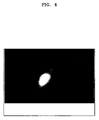
- FIG. 4 is a photo illustrating photoluminescence (PL) characteristics of Si-nanoparticles having a core/shell structure.
- FIG. 1 is a schematic cross-sectional view of a nanoparticle eletroluminescence device according to an embodiment of the present invention.
- the nanoparticle electroluminescence device according to the present disclosure includes a front electrode 20 , a rear electrode 40 , and an emitting layer (EML) 30 interposed between the front electrode 20 and the rear electrode 40 .
- EML emitting layer
- the emitting layer (EML) 30 is an area in which recombination of electrons and holes supplied from both electrodes 20 and 40 is performed and luminescence is produced.
- the EML 30 includes nanoparticles 24 a having a core/shell structure comprising a core formed of silicon and a shell formed of silicon oxide (SiO 2 ) or silicon nitride (Si 3 N 4 ), for example, on the surface of the core.
- the nanoparticles 24 a having the core/shell structure may be manufactured using pyrolysis or laser ablation. A method of generating particles using pyrolysis or laser ablation is generally widely known, and thus, a detailed description thereof will be omitted.
- the manufactured Si-core is thermally processed at a predetermined temperature in an oxygen (O 2 ) or ammonia (NH 3 ) atmosphere so that the nanoparticles 24 a having the core/shell structure in which a shell of silicon oxide or silicon nitride is formed on the surface of the core can be obtained.
- the structure of the nanoparticles 24 a having the core/shell structure is such that, the Si-core is effectively capped by the shell so that the interface characteristics and luminescence characteristics of the Si-core can be improved.
- the diameter of the nanoparticles 24 a is between 1 nm and 10 nm.
- the EML 30 may include a nanoparticle layer 24 formed of nanoparticles 24 a having the core/shell structure and insulating layers 22 a and 22 b formed above and below the nanoparticles 24 , respectively.
- the insulating layers 22 a and 22 b can be formed of silicon oxide (SiO 2 ) or silicon nitride (Si 3 N 4 ).
- the front electrode 20 is formed of a transparent conductive material so that light emitted from the EML 30 can be transmitted.
- a transparent conductive material is indium tin oxide (ITO).
- the rear electrode 40 is formed of a conductive material, for example, Al or Mg.
- EL electroluminescence
- the interface characteristics of the Si-core are improved by effectively capping the core using the shell so that a nanoparticle electroluminescence device having excellent light emission and an improved luminescence efficiency can be obtained
- FIG. 2 is a schematic cross-sectional view of a nanoparticle electroluminescence device according to another embodiment of the present invention.
- FIG. 2 a description of similar elements as those shown in FIG. 1 will be omitted, and like elements denote like reference numerals.
- an EML 31 interposed between the front electrode 20 and the rear electrode 40 includes at least one EML 30 that is the same as the EML 30 illustrated in FIG. 1 .
- the EML 30 illustrated in FIG. 2 includes a plurality of nanoparticle layers 24 formed of nanoparticles 24 a having the core/shell structure and insulating layers 22 a , 22 b , 22 c , and 22 d formed above and below the nanoparticle layers 24 , respectively.
- a plurality of EMLs are formed in this way so that a nanoparticle electroluminescence device is formed having higher light emission than the light emission generated when a single EML is formed.
- FIGS. 3A through 3F illustrate a method of manufacturing a nanoparticle electroluminescence device according to another embodiment of the present invention.
- a transparent substrate 10 is prepared and a front electrode 20 is formed of a transparent conductive material, for example, ITO, on the substrate 10 .
- a lower insulating layer 22 a is formed on the front electrode 20 .
- the transparent substrate 10 can be formed of a material selected from the group consisting of plastic and sapphire etc.
- the lower insulating layer 22 a is generally formed of silicon oxide (SiO 2 ) or silicon nitride (Si 3 N 4 ) but the present invention is not limited to these materials.
- the lower insulating layer 22 a may be formed using a well-known thin film deposition method, for example, chemical vapor deposition (CVD) or physical vapor deposition (PVD).
- CVD chemical vapor deposition
- PVD physical vapor deposition
- nanoparticles 24 a having a core/shell structure comprising a core formed of silicon and a shell formed of silicon oxide (SiO 2 ) or silicon nitride (Si 3 N 4 ), for example, on the surface of the core, are coated on the lower insulating layer 22 a so that a nanoparticle layer 24 is formed.
- the diameter of the nanoparticles 24 a is between 1 nm to 10 nm.
- the nanoparticles 24 a may be formed using pyrolysis or laser ablation. A method of generating particles using pyrolysis or laser ablation is generally widely known, and thus, a detailed description thereof will be omitted.
- the manufactured Si-core is thermally processed at a predetermined temperature in an oxygen (O 2 ) or ammonia (NH 3 ) atmosphere so that the nanoparticles 24 a having the core/shell structure in which a shell of silicon oxide or silicon nitride is formed on the outer surface of the core can be obtained.
- O 2 oxygen
- NH 3 ammonia
- nanoparticles 24 a can be coated using the widely known processes of thermophoresis or electrophoresis, and thus, a detailed description thereof will be omitted.
- an upper insulating layer 22 b and a rear electrode 40 are sequentially stacked on the nanoparticle layer 24 .
- the upper insulating layer 22 b is generally formed of silicon oxide (SiO 2 ) or silicon nitride (Si 3 N 4 ), for example, but the present invention is not limited to these materials and the upper insulating layer 22 b may be formed of other insulating materials.
- the rear electrode 40 is formed of a conductive material, for example, Al or Mg.
- the upper insulating layer 22 b and the rear electrode 40 may be formed using a well-known thin film deposition method, for example, CVD or PVD.
- a nanoparticle electroluminescence device having excellent light emission and an improved luminance efficiency can be obtained.
- the size of the nanoparticles is controlled when manufacturing the nanoparticle electroluminescence device so that a quantum confinement effect can be obtained from the nanoparticles.
- the method of manufacturing the nanoparticle electroluminescence device having the above structure can be easily performed, and costs are low.
- the lower insulating layer 22 a , the nanoparticle layer 24 , and the upper insulating layer 22 b which are sequentially stacked, may form one EML 30 , and at least one emitting layers of the structure of the EML 30 may be further stacked on the EML 30 .
- a plurality of EMLs are formed in this way so that a nanoparticle electroluminescence device is formed having higher light emission than the light emission generated when a single EML 30 is formed.
- FIG. 4 is a photo showing luminescence characteristics of Si-nanoparticles having a core/shell structure.
- the interface characteristics of the Si-core are improved by effectively capping the Si-core by the shell so that the nanoparticle electroluminescence device having excellent light emission and an improved luminescence efficiency can be obtained.
- the EML of the nanoparticle electroluminescence device according to the present disclosure includes nanoparticles having a core/shell structure so that the Si-core is effectively capped by the shell and the interface characteristics and luminescence characteristics of the Si-core can be improved.
Abstract
Description
Claims (10)
Applications Claiming Priority (2)
| Application Number | Priority Date | Filing Date | Title |
|---|---|---|---|
| KR1020050015574A KR100695143B1 (en) | 2005-02-24 | 2005-02-24 | Nanoparticle electroluminescence device and fabrication method of the same |
| KR10-2005-0015574 | 2005-02-24 |
Publications (2)
| Publication Number | Publication Date |
|---|---|
| US20060188707A1 US20060188707A1 (en) | 2006-08-24 |
| US7592618B2 true US7592618B2 (en) | 2009-09-22 |
Family
ID=36913059
Family Applications (1)
| Application Number | Title | Priority Date | Filing Date |
|---|---|---|---|
| US11/356,122 Active 2027-04-20 US7592618B2 (en) | 2005-02-24 | 2006-02-17 | Nanoparticle electroluminescence and method of manufacturing the same |
Country Status (3)
| Country | Link |
|---|---|
| US (1) | US7592618B2 (en) |
| JP (1) | JP2006237595A (en) |
| KR (1) | KR100695143B1 (en) |
Cited By (14)
| Publication number | Priority date | Publication date | Assignee | Title |
|---|---|---|---|---|
| US20070181906A1 (en) * | 2005-12-28 | 2007-08-09 | George Chik | Carbon passivation in solid-state light emitters |
| US20090206323A1 (en) * | 2008-02-18 | 2009-08-20 | Shin Yokoyama | Light-emitting element and method for manufacturing the same |
| US20100176370A1 (en) * | 2008-03-26 | 2010-07-15 | Shin Yokoyama | Light-emitting device and method for manufacturing the same |
| US20100283036A1 (en) * | 2007-07-23 | 2010-11-11 | Seth Coe-Sullivan | Quantum dot light enhancement substrate and lighting device including same |
| US20110241042A1 (en) * | 2010-04-02 | 2011-10-06 | Miin-Jang Chen | Nanocrystal-based optoelectronic device and method of fabricating the same |
| US8981339B2 (en) | 2009-08-14 | 2015-03-17 | Qd Vision, Inc. | Lighting devices, an optical component for a lighting device, and methods |
| US9054329B2 (en) | 2006-06-02 | 2015-06-09 | Qd Vision, Inc. | Light-emitting devices and displays with improved performance |
| US9064693B2 (en) | 2010-03-01 | 2015-06-23 | Kirsteen Mgmt. Group Llc | Deposition of thin film dielectrics and light emitting nano-layer structures |
| US9140844B2 (en) | 2008-05-06 | 2015-09-22 | Qd Vision, Inc. | Optical components, systems including an optical component, and devices |
| US9167659B2 (en) | 2008-05-06 | 2015-10-20 | Qd Vision, Inc. | Solid state lighting devices including quantum confined semiconductor nanoparticles, an optical component for a solid state lighting device, and methods |
| US9207385B2 (en) | 2008-05-06 | 2015-12-08 | Qd Vision, Inc. | Lighting systems and devices including same |
| US9406765B1 (en) * | 2015-07-29 | 2016-08-02 | Nano And Advanced Materials Institute Limited | Hybrid dielectric non-volatile memory with nano particles (Si/SiO2 core/shell) as charge trapping layer |
| US10164205B2 (en) | 2008-04-03 | 2018-12-25 | Samsung Research America, Inc. | Device including quantum dots |
| US10333090B2 (en) | 2008-04-03 | 2019-06-25 | Samsung Research America, Inc. | Light-emitting device including quantum dots |
Families Citing this family (12)
| Publication number | Priority date | Publication date | Assignee | Title |
|---|---|---|---|---|
| KR101361861B1 (en) * | 2006-11-08 | 2014-02-12 | 엘지디스플레이 주식회사 | Organic light emitting diodes and method of manufacturing the same |
| US20080191193A1 (en) * | 2007-01-22 | 2008-08-14 | Xuegeng Li | In situ modification of group iv nanoparticles using gas phase nanoparticle reactors |
| US20090026421A1 (en) * | 2007-01-22 | 2009-01-29 | Xuegeng Li | Optimized laser pyrolysis reactor and methods therefor |
| WO2008118865A2 (en) * | 2007-03-27 | 2008-10-02 | Innovalight, Inc. | Optimized laser pyrolysis reactor and methods therefor |
| KR100853087B1 (en) * | 2007-04-26 | 2008-08-19 | 삼성전자주식회사 | Nanocrystal, preparation method thereof and electronic devices comprising the same |
| JP2009087782A (en) * | 2007-09-28 | 2009-04-23 | Dainippon Printing Co Ltd | Manufacturing method of electroluminescent element |
| JP5704899B2 (en) * | 2010-11-16 | 2015-04-22 | キヤノン株式会社 | Active layer used in silicon light emitting device and method for manufacturing the active layer |
| JP5822543B2 (en) * | 2011-06-06 | 2015-11-24 | キヤノン株式会社 | Light emitting element |
| CN103601194B (en) * | 2013-11-19 | 2019-04-12 | 肖彦社 | A method of regulation nano-silicon pattern and structure |
| CN105552244B (en) * | 2016-02-17 | 2018-09-11 | 京东方科技集团股份有限公司 | A kind of luminescent device and preparation method thereof, display device |
| CN109671855A (en) * | 2018-12-20 | 2019-04-23 | 电子科技大学 | Perovskite luminescent device and preparation method thereof based on ultra-thin dielectric wall |
| EP4006994A1 (en) * | 2020-11-26 | 2022-06-01 | Stmicroelectronics (Grenoble 2) Sas | Optoelectronic device |
Citations (4)
| Publication number | Priority date | Publication date | Assignee | Title |
|---|---|---|---|---|
| JPH09181353A (en) | 1995-12-25 | 1997-07-11 | Toshiba Corp | Manufacture of si fine particle and manufacture of si fine particle thin film, and light-emitting device provided with si fine particle thin film |
| US20030230629A1 (en) * | 2002-06-18 | 2003-12-18 | Bourianoff George I. | Electro-optical nanocrystal memory device |
| US20040252488A1 (en) * | 2003-04-01 | 2004-12-16 | Innovalight | Light-emitting ceiling tile |
| US7301172B2 (en) * | 2004-04-07 | 2007-11-27 | California Institute Of Technology | Sequentially charged nanocrystal light emitting device |
Family Cites Families (6)
| Publication number | Priority date | Publication date | Assignee | Title |
|---|---|---|---|---|
| JP2001234163A (en) * | 2000-02-25 | 2001-08-28 | Sony Corp | Luminous crystalline particle, luminous crystalline particle composition, display panel and flat-surface display device |
| KR100495625B1 (en) * | 2002-04-23 | 2005-06-16 | 대주전자재료 주식회사 | Conjugated polymer-inorganic particulate composite composition for luminescent layer of organic electroluminescence device |
| JP2004164855A (en) | 2002-09-18 | 2004-06-10 | Kura Gijutsu Kenkyusho:Kk | Electroluminescent element, electroscope using electroluminescent element, conduction display power line, and circuit board defect inspection device |
| KR100888470B1 (en) * | 2002-12-24 | 2009-03-12 | 삼성모바일디스플레이주식회사 | Inorganic electroluminescence device |
| JP2004259546A (en) | 2003-02-25 | 2004-09-16 | Seiko Precision Inc | Inorganic el element |
| JP2004259545A (en) | 2003-02-25 | 2004-09-16 | Seiko Precision Inc | Manufacturing method of inorganic electroluminescent element |
-
2005
- 2005-02-24 KR KR1020050015574A patent/KR100695143B1/en active IP Right Grant
-
2006
- 2006-02-07 JP JP2006030151A patent/JP2006237595A/en not_active Withdrawn
- 2006-02-17 US US11/356,122 patent/US7592618B2/en active Active
Patent Citations (4)
| Publication number | Priority date | Publication date | Assignee | Title |
|---|---|---|---|---|
| JPH09181353A (en) | 1995-12-25 | 1997-07-11 | Toshiba Corp | Manufacture of si fine particle and manufacture of si fine particle thin film, and light-emitting device provided with si fine particle thin film |
| US20030230629A1 (en) * | 2002-06-18 | 2003-12-18 | Bourianoff George I. | Electro-optical nanocrystal memory device |
| US20040252488A1 (en) * | 2003-04-01 | 2004-12-16 | Innovalight | Light-emitting ceiling tile |
| US7301172B2 (en) * | 2004-04-07 | 2007-11-27 | California Institute Of Technology | Sequentially charged nanocrystal light emitting device |
Cited By (33)
| Publication number | Priority date | Publication date | Assignee | Title |
|---|---|---|---|---|
| US7679102B2 (en) * | 2005-12-28 | 2010-03-16 | Group Iv Semiconductor, Inc. | Carbon passivation in solid-state light emitters |
| US20070181906A1 (en) * | 2005-12-28 | 2007-08-09 | George Chik | Carbon passivation in solid-state light emitters |
| US9054329B2 (en) | 2006-06-02 | 2015-06-09 | Qd Vision, Inc. | Light-emitting devices and displays with improved performance |
| US10770619B2 (en) | 2006-06-02 | 2020-09-08 | Samsung Electronics Co., Ltd. | Light-emitting devices and displays with improved performance |
| US10297713B2 (en) | 2006-06-02 | 2019-05-21 | Samsung Electronics Co., Ltd. | Light-emitting devices and displays with improved performance |
| US9853184B2 (en) | 2006-06-02 | 2017-12-26 | Samsung Electronics Co., Ltd. | Light-emitting devices and displays with improved performance |
| US20100283036A1 (en) * | 2007-07-23 | 2010-11-11 | Seth Coe-Sullivan | Quantum dot light enhancement substrate and lighting device including same |
| US10096744B2 (en) | 2007-07-23 | 2018-10-09 | Samsung Electronics Co., Ltd. | Quantum dot light enhancement substrate and lighting device including same |
| US9680054B2 (en) | 2007-07-23 | 2017-06-13 | Samsung Electronics Co., Ltd. | Quantum dot light enhancement substrate and lighting device including same |
| US8405063B2 (en) * | 2007-07-23 | 2013-03-26 | Qd Vision, Inc. | Quantum dot light enhancement substrate and lighting device including same |
| US8759850B2 (en) | 2007-07-23 | 2014-06-24 | Qd Vision, Inc. | Quantum dot light enhancement substrate |
| US9276168B2 (en) | 2007-07-23 | 2016-03-01 | Qd Vision, Inc. | Quantum dot light enhancement substrate and lighting device including same |
| US8368046B2 (en) | 2008-02-18 | 2013-02-05 | Hiroshima University | Light-emitting element |
| US20090206323A1 (en) * | 2008-02-18 | 2009-08-20 | Shin Yokoyama | Light-emitting element and method for manufacturing the same |
| US8980658B2 (en) | 2008-02-18 | 2015-03-17 | Hiroshima University | Light-emitting element |
| US8330141B2 (en) | 2008-03-26 | 2012-12-11 | Hiroshima University | Light-emitting device |
| US20100176370A1 (en) * | 2008-03-26 | 2010-07-15 | Shin Yokoyama | Light-emitting device and method for manufacturing the same |
| US8044382B2 (en) * | 2008-03-26 | 2011-10-25 | Hiroshima University | Light-emitting device and method for manufacturing the same |
| US11005058B2 (en) | 2008-04-03 | 2021-05-11 | Samsung Research America, Inc. | Light-emitting device including quantum dots |
| US10333090B2 (en) | 2008-04-03 | 2019-06-25 | Samsung Research America, Inc. | Light-emitting device including quantum dots |
| US10164205B2 (en) | 2008-04-03 | 2018-12-25 | Samsung Research America, Inc. | Device including quantum dots |
| US9946004B2 (en) | 2008-05-06 | 2018-04-17 | Samsung Electronics Co., Ltd. | Lighting systems and devices including same |
| US10145539B2 (en) | 2008-05-06 | 2018-12-04 | Samsung Electronics Co., Ltd. | Solid state lighting devices including quantum confined semiconductor nanoparticles, an optical component for a solid state lighting device, and methods |
| US9207385B2 (en) | 2008-05-06 | 2015-12-08 | Qd Vision, Inc. | Lighting systems and devices including same |
| US9167659B2 (en) | 2008-05-06 | 2015-10-20 | Qd Vision, Inc. | Solid state lighting devices including quantum confined semiconductor nanoparticles, an optical component for a solid state lighting device, and methods |
| US10359555B2 (en) | 2008-05-06 | 2019-07-23 | Samsung Electronics Co., Ltd. | Lighting systems and devices including same |
| US10627561B2 (en) | 2008-05-06 | 2020-04-21 | Samsung Electronics Co., Ltd. | Lighting systems and devices including same |
| US9140844B2 (en) | 2008-05-06 | 2015-09-22 | Qd Vision, Inc. | Optical components, systems including an optical component, and devices |
| US9391244B2 (en) | 2009-08-14 | 2016-07-12 | Qd Vision, Inc. | Lighting devices, an optical component for a lighting device, and methods |
| US8981339B2 (en) | 2009-08-14 | 2015-03-17 | Qd Vision, Inc. | Lighting devices, an optical component for a lighting device, and methods |
| US9064693B2 (en) | 2010-03-01 | 2015-06-23 | Kirsteen Mgmt. Group Llc | Deposition of thin film dielectrics and light emitting nano-layer structures |
| US20110241042A1 (en) * | 2010-04-02 | 2011-10-06 | Miin-Jang Chen | Nanocrystal-based optoelectronic device and method of fabricating the same |
| US9406765B1 (en) * | 2015-07-29 | 2016-08-02 | Nano And Advanced Materials Institute Limited | Hybrid dielectric non-volatile memory with nano particles (Si/SiO2 core/shell) as charge trapping layer |
Also Published As
| Publication number | Publication date |
|---|---|
| KR20060094429A (en) | 2006-08-29 |
| US20060188707A1 (en) | 2006-08-24 |
| JP2006237595A (en) | 2006-09-07 |
| KR100695143B1 (en) | 2007-03-14 |
Similar Documents
| Publication | Publication Date | Title |
|---|---|---|
| US7592618B2 (en) | Nanoparticle electroluminescence and method of manufacturing the same | |
| Shi et al. | Localized surface plasmon enhanced all‐inorganic perovskite quantum dot light‐emitting diodes based on coaxial core/shell heterojunction architecture | |
| US8581230B2 (en) | Light-emitting device having enhanced luminescence by using surface plasmon resonance and method of fabricating the same | |
| KR101357045B1 (en) | Tunable Light Emitting Diode using Graphene conjugated Metal oxide semiconductor-Graphene core-shell Quantum dots and its fabrication process thereof | |
| EP2150996B1 (en) | Electroluminescent device having improved light output | |
| CN100550446C (en) | With the light-emitting device of conductive nano rod as transparency electrode | |
| KR101304635B1 (en) | Inorganic electroluminescent diode and process for preparing the same | |
| KR101794082B1 (en) | Quantum dot light emitting diode device comprising quantum dot emitting layer with substituted ligand by dendrimer having amine groups, and method for manufacturing the same | |
| US20090039764A1 (en) | Quantum Dot Light-Emitting Diode Comprising Inorganic Electron Transport Layer | |
| EP2040514A1 (en) | Quantum dot light emitting inorganic el element | |
| KR20080103568A (en) | Nanostructured electroluminescent device and display | |
| KR102156760B1 (en) | Quantum dot light emitting display device and method for fabricating the same | |
| US7589464B2 (en) | Nanotip electrode electroluminescence device with contoured phosphor layer | |
| JP2008543074A (en) | Organic electroluminescent light source | |
| KR101097342B1 (en) | Quantum dot organic light emitting device and method of formation thereof | |
| KR20120029096A (en) | Quantum-dot light emitting diode and method for fabrication the same | |
| WO2020174594A1 (en) | Light-emitting device, display device | |
| KR20150107249A (en) | A light-emitting diode with single layer quantum dot using polymer surface modification layer | |
| KR101656927B1 (en) | Light Emitting Device and Method Of Manufacturing Electron Transport layer | |
| KR101765183B1 (en) | Light extraction layer for light emitting apparatus and method of forming the light extraction layer | |
| CN107658385A (en) | quantum dot film and preparation method thereof | |
| EP3122155B1 (en) | Light emitting device | |
| KR101450858B1 (en) | Organic electroluminescent device and fabracation method by using graphene oxide | |
| KR101560088B1 (en) | Light Emitting Device and Method Of Manufacturing Light Emitting Device | |
| KR101427460B1 (en) | Organic Light Emitting Device And Method for Manufacturing The Same |
Legal Events
| Date | Code | Title | Description |
|---|---|---|---|
| AS | Assignment |
Owner name: SAMSUNG ELECTRONICS CO., LTD., KOREA, REPUBLIC OF Free format text: ASSIGNMENT OF ASSIGNORS INTEREST;ASSIGNORS:KHANG, YOON-HO;LEE, EUN-HYE;LEE, KYO-YEOL;AND OTHERS;REEL/FRAME:017602/0980 Effective date: 20060217 |
|
| STCF | Information on status: patent grant |
Free format text: PATENTED CASE |
|
| FEPP | Fee payment procedure |
Free format text: PAYOR NUMBER ASSIGNED (ORIGINAL EVENT CODE: ASPN); ENTITY STATUS OF PATENT OWNER: LARGE ENTITY |
|
| FEPP | Fee payment procedure |
Free format text: PAYER NUMBER DE-ASSIGNED (ORIGINAL EVENT CODE: RMPN); ENTITY STATUS OF PATENT OWNER: LARGE ENTITY Free format text: PAYOR NUMBER ASSIGNED (ORIGINAL EVENT CODE: ASPN); ENTITY STATUS OF PATENT OWNER: LARGE ENTITY |
|
| FPAY | Fee payment |
Year of fee payment: 4 |
|
| FPAY | Fee payment |
Year of fee payment: 8 |
|
| MAFP | Maintenance fee payment |
Free format text: PAYMENT OF MAINTENANCE FEE, 12TH YEAR, LARGE ENTITY (ORIGINAL EVENT CODE: M1553); ENTITY STATUS OF PATENT OWNER: LARGE ENTITY Year of fee payment: 12 |