US7460165B2 - Photo-array layout for monitoring image statistics - Google Patents
Photo-array layout for monitoring image statistics Download PDFInfo
- Publication number
- US7460165B2 US7460165B2 US10/754,434 US75443404A US7460165B2 US 7460165 B2 US7460165 B2 US 7460165B2 US 75443404 A US75443404 A US 75443404A US 7460165 B2 US7460165 B2 US 7460165B2
- Authority
- US
- United States
- Prior art keywords
- sensors
- sensor array
- sensor
- region
- area
- Prior art date
- Legal status (The legal status is an assumption and is not a legal conclusion. Google has not performed a legal analysis and makes no representation as to the accuracy of the status listed.)
- Active, expires
Links
- 238000012544 monitoring process Methods 0.000 title description 2
- 239000000872 buffer Substances 0.000 claims description 2
- 238000003384 imaging method Methods 0.000 abstract description 10
- 238000013461 design Methods 0.000 abstract description 8
- 238000013459 approach Methods 0.000 description 6
- 238000000034 method Methods 0.000 description 4
- 239000000463 material Substances 0.000 description 2
- 230000003287 optical effect Effects 0.000 description 2
- 238000012545 processing Methods 0.000 description 2
- 239000000758 substrate Substances 0.000 description 2
- XUIMIQQOPSSXEZ-UHFFFAOYSA-N Silicon Chemical compound [Si] XUIMIQQOPSSXEZ-UHFFFAOYSA-N 0.000 description 1
- 238000003491 array Methods 0.000 description 1
- 230000001413 cellular effect Effects 0.000 description 1
- 230000000295 complement effect Effects 0.000 description 1
- 230000003247 decreasing effect Effects 0.000 description 1
- 238000010586 diagram Methods 0.000 description 1
- 229910044991 metal oxide Inorganic materials 0.000 description 1
- 150000004706 metal oxides Chemical class 0.000 description 1
- 238000010295 mobile communication Methods 0.000 description 1
- 239000004065 semiconductor Substances 0.000 description 1
- 229910052710 silicon Inorganic materials 0.000 description 1
- 239000010703 silicon Substances 0.000 description 1
Images


Classifications
-
- H—ELECTRICITY
- H01—ELECTRIC ELEMENTS
- H01L—SEMICONDUCTOR DEVICES NOT COVERED BY CLASS H10
- H01L27/00—Devices consisting of a plurality of semiconductor or other solid-state components formed in or on a common substrate
- H01L27/14—Devices consisting of a plurality of semiconductor or other solid-state components formed in or on a common substrate including semiconductor components sensitive to infrared radiation, light, electromagnetic radiation of shorter wavelength or corpuscular radiation and specially adapted either for the conversion of the energy of such radiation into electrical energy or for the control of electrical energy by such radiation
- H01L27/144—Devices controlled by radiation
- H01L27/146—Imager structures
- H01L27/14601—Structural or functional details thereof
- H01L27/14603—Special geometry or disposition of pixel-elements, address-lines or gate-electrodes
-
- H—ELECTRICITY
- H04—ELECTRIC COMMUNICATION TECHNIQUE
- H04N—PICTORIAL COMMUNICATION, e.g. TELEVISION
- H04N23/00—Cameras or camera modules comprising electronic image sensors; Control thereof
- H04N23/10—Cameras or camera modules comprising electronic image sensors; Control thereof for generating image signals from different wavelengths
-
- H—ELECTRICITY
- H04—ELECTRIC COMMUNICATION TECHNIQUE
- H04N—PICTORIAL COMMUNICATION, e.g. TELEVISION
- H04N23/00—Cameras or camera modules comprising electronic image sensors; Control thereof
- H04N23/70—Circuitry for compensating brightness variation in the scene
- H04N23/71—Circuitry for evaluating the brightness variation
-
- H—ELECTRICITY
- H04—ELECTRIC COMMUNICATION TECHNIQUE
- H04N—PICTORIAL COMMUNICATION, e.g. TELEVISION
- H04N25/00—Circuitry of solid-state image sensors [SSIS]; Control thereof
-
- H—ELECTRICITY
- H04—ELECTRIC COMMUNICATION TECHNIQUE
- H04N—PICTORIAL COMMUNICATION, e.g. TELEVISION
- H04N25/00—Circuitry of solid-state image sensors [SSIS]; Control thereof
- H04N25/60—Noise processing, e.g. detecting, correcting, reducing or removing noise
-
- H—ELECTRICITY
- H04—ELECTRIC COMMUNICATION TECHNIQUE
- H04N—PICTORIAL COMMUNICATION, e.g. TELEVISION
- H04N3/00—Scanning details of television systems; Combination thereof with generation of supply voltages
- H04N3/10—Scanning details of television systems; Combination thereof with generation of supply voltages by means not exclusively optical-mechanical
- H04N3/14—Scanning details of television systems; Combination thereof with generation of supply voltages by means not exclusively optical-mechanical by means of electrically scanned solid-state devices
- H04N3/15—Scanning details of television systems; Combination thereof with generation of supply voltages by means not exclusively optical-mechanical by means of electrically scanned solid-state devices for picture signal generation
-
- H—ELECTRICITY
- H01—ELECTRIC ELEMENTS
- H01L—SEMICONDUCTOR DEVICES NOT COVERED BY CLASS H10
- H01L27/00—Devices consisting of a plurality of semiconductor or other solid-state components formed in or on a common substrate
- H01L27/14—Devices consisting of a plurality of semiconductor or other solid-state components formed in or on a common substrate including semiconductor components sensitive to infrared radiation, light, electromagnetic radiation of shorter wavelength or corpuscular radiation and specially adapted either for the conversion of the energy of such radiation into electrical energy or for the control of electrical energy by such radiation
- H01L27/144—Devices controlled by radiation
- H01L27/146—Imager structures
- H01L27/14601—Structural or functional details thereof
- H01L27/14625—Optical elements or arrangements associated with the device
Definitions
- the present invention relates to digital imaging systems. More particularly, the present invention relates to the art of detecting image statistics.
- a scene is captured by using a lens to direct light from the scene on an array of sensors, or photo-detectors, such as an array of photodiodes.
- Each sensor of the sensor array detects light from a tiny portion of the scene.
- the detected light is converted into an electrical signal, and then into a digital value indicating the intensity of the light detected by that sensor.
- the digital values from all of the sensors of the sensor array are combined to form an image of the scene. For this reason, the sensor array is referred to as the image sensor array.
- FIG. 1 illustrates a single sensor 10 including an active area 12 and a support hardware area 14 .
- the active area 12 can be fabricated generally in the shape of a cross and the support hardware area 14 generally having a rectangular shape and adjoining the active area 12 .
- the active area 12 includes a photo-detector to capture light to produce a corresponding electrical signal.
- the electrical signal is processed by support hardware in the support hardware area 14 .
- the support hardware can include, for example, amplifiers, buffers, and converters. Light falling on the support hardware area 14 portion of the sensor 10 is lost as there are no photo-detectors in that area. For this reason, the support hardware area 15 is designed to occupy smallest area possible and covers smaller area than the area occupied by its active area 12 . Additionally, the support hardware area 14 adjoins the active area 12 at a predetermined direction 17 relative to the active area 12 . In the illustrated sensor 10 , the support hardware area 14 adjoins the active area 12 at upper right direction relative to the active area 12 .
- the active area 10 can have a lateral extent 13 in the order of microns or tens of microns, for example, approximately 60 microns.
- the hardware support area 14 of the sensor 10 can have a lateral extent 15 in the order of microns or tens of microns, for example, approximately 20 microns.
- CMOS complementary metal-oxide semiconductor
- CCD charge-coupled devices
- An image sensor array often includes a rectangular layout of many hundreds of thousands, millions, or even greater number of sensors, each sensor providing a digital value, or a pixel, of information.
- a rectangular image sensor array arranged in 640 columns and 480 rows has 307,200 sensors, or pixels.
- a digital value from a sensor is defined as a pixel of the image.
- each sensor, or pixel is referred generically as P i,j where i,j indicates that the pixel is located at i th column at j th row of a rectangular image sensor array having M columns and N rows, the value of i ranging from 1 to M, inclusive, and the value of j ranging from 1 to N, inclusive.
- FIG. 2 illustrates a sample sensor array 20 including a rectangular array of sensors, each sensor having the configuration of the sensor 10 of FIG. 1 .
- the sensor array 20 includes 36 sensors in a six by six rectangular configuration.
- Each sensor of the sensor array 20 having a cross shaped active area (for example, active area 22 ) adjoining a support hardware area (for example, support hardware area 24 ) to its upper right direction 26 .
- each of the sensors of the image sensor array is initialized to an initial value. Then, the image sensor array is exposed to light from the scene for a period of time, the exposure period. After the exposure, the values of the sensors are read. The values from the sensors are combined to form an image of the scene. For best results, it is desirable to know various characteristics or statistics of the light from the scene to determine the operations of the image sensor array. For example, it is desirable to know the intensity of the light from the scene to determine the exposure period. For convenience, the characteristics or statistics of the light from the scene is referred to as “image statistics” in this document. For example, image statistics may include average pixel value.
- a digital imaging device includes a reference detector positioned proximal to its image sensor array. Further, the reference detector is provided with its own lens and optical path through which light from the scene enters. In this design, the reference detector is operated substantially simultaneously as the image sensor array to collect image statistics.
- the reference detector can be a single detector or an array of detectors.
- the cost, the complexity, and the bulk of the digital imaging device are increased and the reliability is decreased. This is because the reference detector needs its own lens and optical path, introducing additional components to the digital imaging device.
- the image exposed to the reference detector is not identical to the image exposed to the image sensor array. Accordingly, the image statistics gather from the reference detector may only be marginally applicable to the image captured by the image sensor array, or the image statistics gather from the reference detector may not be applicable or even useful at all.
- a beam splitter is used to split the light from a scene such that a first portion of the light from the scene is directed toward the image sensor array while a second portion of the light from the scene is directed toward a reference detector.
- the reference detector senses the second portion of the light to gather images statistics.
- the image statistics can be used to determine the exposure period of the image sensor array or various processing parameters for processing of the captured image.
- both the image sensor array and the reference detector see the identical scene. However, some of the light (the second portion) from the scene is lost to the image sensor because it is directed toward the reference detector.
- the image sensor array is exposed (to the scene to be captured) twice in succession. During the first exposure, image statistics are gathered using the image sensor array. During the second exposure, the scene is captured as an image. In this design, no additional components are required, and the light from the scene is not apportioned. However, this approach requires two exposures of the image sensor array. Moreover, the lighting condition may have changed from the first exposure to the second exposure.
- one or more sensors at the edges of the image sensor array are used as the reference detector to gather image statistics.
- image statistics do not reflect the characteristics of the image near its center which is often the most interesting part of the image.
- a photo sensor array includes an array of sensors, an array of sensors, each sensor of the sensor array having an active area adapted to detect light and a support hardware area adjoining the active area.
- the support hardware area of each sensor adjoins the active area of the sensor in a direction that is radially away from center of the sensor array whereby at least one freed area is defined within the sensor array.
- a photo sensor array in a second embodiment of the present invention, includes an array of sensors and a reference detector. Each sensor of the sensor array has an active area adapted to detect light and a support hardware area connected to the active area.
- the reference detector is located between a first sensor and a second sensor of the sensor array where the first sensor has a first active area adapted to detect light and a first support hardware area is connected to the first active area, the first support hardware area connected to the first active area in a first direction radially away from the reference detector.
- the second sensor has a second active area adapted to detect light and a second support hardware area connected to the second active area, the second support hardware area is connected to the second active area in a second direction radially away from the reference detector.
- an image capture apparatus in a third embodiment of the present invention, includes a lens adapted to focus a scene onto an image sensor array.
- the photo sensor array includes an array of sensors, an array of sensors, each sensor of the sensor array having an active area adapted to detect light and a support hardware area adjoining the active area.
- the support hardware area of each sensor adjoins the active area of the sensor in a direction that is radially away from center of the sensor array whereby at least one freed area is defined within the sensor array.
- FIG. 1 illustrates a sample photo-sensor
- FIG. 2 illustrates a sample photo-sensor array including an array of photo-sensors of FIG. 1 ;
- FIG. 3 illustrates a photo-sensor array according to one embodiment of the present invention
- FIG. 4 illustrates a photo-sensor array according to another embodiment of the present invention.
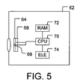
- FIG. 5 illustrates an image capture apparatus according to one embodiment of the present invention.
- FIGS. 1 through 5 illustrate various embodiments of the present invention.
- some sizes of structures or portions may be exaggerated relative to sizes of other structures or portions for illustrative purposes and, thus, are provided to illustrate the general structures of the present invention.
- various aspects of the present invention are described with reference to a structure or a portion positioned “above” or “right of” relative to other structures, portions, or both.
- relative terms and phrases such as “above” or “right of” are used herein to describe one structure's or portion's relationship to another structure or portion as illustrated in the Figures.
- embodiments of the present invention are exemplified by an array of sensors, each sensor of the sensor array having an active area adapted to detect light and a support hardware area adjoining the active area in a predetermined direction.
- the support hardware area of each sensor adjoins the active area of the sensor in the same direction.
- the support hardware area of each sensor adjoins the active area of the sensor in a direction that is radially away from center of the sensor array whereby at least one freed area is defined within the sensor array.
- a reference detector can be fabricated within the freed area to gather the image statistics.
- An imaging apparatus having a sensor array embodying the present design has a number of advantages over the prior art. Firstly, the reference detector is built within the image sensor array; therefore, a separate reference detector and its own optics components are not needed. Secondly, reference detector is exposed (to light from the scene to be captured) at the same time as the image sensor array; therefore, only one exposure to the scene is need. Thirdly, the reference detector is exposed to the same scene as the scene exposed to the rest of the image sensor array; therefore, image statistics gathered using the reference detector is applicable. Finally, the reference detector can be used to gather image statistics from the center or other useful or interesting portions of the image sensor array; therefore, image statistics is gathered at the most interesting portions of the imaging sensor array.
- FIG. 3 illustrates a first embodiment of the present invention as a photo-sensor array 30 , for example a CMOS sensor array.
- the sensor array 30 as illustrated, for simplicity, as a rectangular grid of six by six sensors. However, in actual implementation, the sensor array 30 can have hundreds, thousands, or even more sensors per each row, column, or both.
- Each sensor of the sensor array 30 has an active area and an adjoining support hardware area and is configured similar to the sensor 10 of FIG. 1 . However, here, the support hardware area of each sensor adjoins the active area of the sensor in a direction that is radially away from center of the sensor array 30 whereby at least one freed area is defined within said sensor array.
- the sensor array 30 (a physical object occupying a definable space) defines a center of its sensing area. In FIG. 3 , the center is illustrated as a point 32 .
- the support hardware area sensor adjoins the active area of the sensor in a direction that is radially away from the center 32 of the sensor array 30 .
- the direction, for each sensor, in which the support hardware area adjoins the active area depends on the sensor's location relative to the desired location of the freed area. In the illustrated example, the desired location of the freed area is the center 32 of the sensor array 30 . Accordingly, the direction, for each sensor, in which the support hardware area adjoins the active area depends on which quadrant of the sensor array 30 within which the sensor is located.
- a first sensor 34 located within the first quadrant 30 a
- its hardware support area 34 s adjoins its active area 34 a in a direction 34 d (indicated by an arrow 34 d ) that is radially away from the center 32 of the sensor array 30 .
- a second sensor 36 located within the first quadrant 30 a
- its hardware support area 36 s adjoins its active area 36 a in a direction 36 d (indicated by an arrow 36 d ) that is radially away from the center 32 of the sensor array 30 .
- a third sensor 38 located within the first quadrant 30 a
- its hardware support area 38 s adjoins its active area 38 a in a direction 38 d (indicated by an arrow 38 d ) that is radially away from the center 32 of the sensor array 30 .
- its hardware support area 40 s adjoins its active area 40 a in a direction 40 d (indicated by an arrow 40 d ) that is radially away from the center 32 of the sensor array 30 .
- the freed areas 42 are areas which were used as support hardware areas in the prior art designs as illustrated in FIG. 2 .
- the support hardware area By positioning, for each sensor of the sensor array, the support hardware area radially away from the center 32 , the freed areas 42 become unoccupied and the sensors define a plurality of freed areas within the sensor array 30 .
- a reference detector can be fabricated in one or more freed areas 42 .
- a reference detector 44 is built in and occupies the freed areas 42 b , 42 c , 42 d , 42 g , and 42 h .
- the reference detector 44 can be a photo-detector and have same or similar circuits as the active areas of the sensors of the sensor array 30 .
- the photo-detectors occupying these freed areas ( 42 b , 42 c , 42 d , 42 g , and 42 h ) can be electrically connected to form a single reference detector 44 .
- the electrical connection is not illustrated in the Figures can be accomplished in layers under or over the sensor array 30 depending on embodiment.
- the reference detector 44 can be positioned substantially at the center 32 of the sensor array 30 .
- the reference detector 44 is positioned between the first sensor 34 and the second sensor 36 as well as between the third sensor 38 and a fourth sensor 40 .
- each of these sensors 34 , 36 , 38 , and 40 has a support hardware area connected to its active area adjoining its active area in a direction radially away from the reference detector 44 . Not all freed areas need be used for a reference detector. In fact, some freed areas ( 42 a , 42 e , 42 f , and 42 i ) are not used for the reference detector.
- FIG. 4 An embodiment of the invention having certain alternate configuration is shown in FIG. 4 . Portions of this embodiment are similar to corresponding portions shown in FIG. 3 . For convenience, portions in FIG. 4 that are similar to corresponding portions in FIG. 3 are assigned the same reference numerals and different components are assigned different reference numerals.
- a sensor array 50 includes a plurality of reference detectors, some reference detector occupying a subset of freed areas. As with the sensor array 30 of FIG. 3 , the sensor array 50 defines freed areas 42 a , 42 b , 42 c , 42 d , 42 e , 42 f , 42 g , 42 h , and 42 i (collectively, “freed areas 42 ”).
- a first reference detector 52 occupies freed areas 42 a and 42 b . These freed areas 42 a and 42 b can be fabricated having photo-detector circuits and electrically connected to form the first reference detector 52 .
- freed areas 42 a and 42 b form a subset of the freed areas 42 available due to the inventive design layout of the present invention discussed above.
- a second reference detector 54 occupies freed areas 42 d and 42 e
- a third reference detector 56 occupies freed areas 42 f and 42 g
- a fourth reference detector 58 occupies freed areas 42 h and 42 i.
- the sensor array 50 can include one or more edge reference detectors along the edges of the sensor array 50 .
- each edge detector occupying edge areas electrically connected.
- the multiple edge areas can be connected to form a single edge reference detector to gather image statistics.
- each of the edge areas can be operated as an individual reference detector to gather image statistics.
- FIG. 5 illustrates a simplified schematic diagram of an image capture apparatus 62 such as, for example, a digital camera, personal digital assistant (PDA), or a mobile communication device such as a cellular camera.
- the apparatus 62 has a lens that directs or focuses a scene to be captured onto an image sensor array 64 , the image sensor array 64 including a reference detector 66 .
- the image sensor array 64 can be configured as the image sensor array 30 of FIG. 3 or the image sensor array 50 of FIG. 4 .
- the sensor array 64 is typically fabricated on a substrate 68 such as silicon substrate 68 .
- the image sensor array 64 is connected to a processor 70 that processes data from the image sensor array 64 .
- the processor can be connected to storage 72 and other electronic circuits 74 to implement other functions of the apparatus 62 .
Abstract
Description
Claims (20)
Priority Applications (4)
| Application Number | Priority Date | Filing Date | Title |
|---|---|---|---|
| US10/754,434 US7460165B2 (en) | 2004-01-09 | 2004-01-09 | Photo-array layout for monitoring image statistics |
| TW093127427A TW200524149A (en) | 2004-01-09 | 2004-09-10 | Photo-array layout for monitoring image statistics |
| GB0427953A GB2409944B (en) | 2004-01-09 | 2004-12-21 | Photo-array layout for monitoring image statistics |
| JP2005001363A JP2005197747A (en) | 2004-01-09 | 2005-01-06 | Photosensor array layout for monitoring image statistics |
Applications Claiming Priority (1)
| Application Number | Priority Date | Filing Date | Title |
|---|---|---|---|
| US10/754,434 US7460165B2 (en) | 2004-01-09 | 2004-01-09 | Photo-array layout for monitoring image statistics |
Publications (2)
| Publication Number | Publication Date |
|---|---|
| US20050151864A1 US20050151864A1 (en) | 2005-07-14 |
| US7460165B2 true US7460165B2 (en) | 2008-12-02 |
Family
ID=34116896
Family Applications (1)
| Application Number | Title | Priority Date | Filing Date |
|---|---|---|---|
| US10/754,434 Active 2026-01-19 US7460165B2 (en) | 2004-01-09 | 2004-01-09 | Photo-array layout for monitoring image statistics |
Country Status (4)
| Country | Link |
|---|---|
| US (1) | US7460165B2 (en) |
| JP (1) | JP2005197747A (en) |
| GB (1) | GB2409944B (en) |
| TW (1) | TW200524149A (en) |
Cited By (2)
| Publication number | Priority date | Publication date | Assignee | Title |
|---|---|---|---|---|
| US8420995B2 (en) | 2009-04-01 | 2013-04-16 | Hamamatsu Photonics K.K. | Solid-state imaging device |
| US10331963B2 (en) * | 2015-06-30 | 2019-06-25 | Denso Corporation | Camera apparatus and in-vehicle system capturing images for vehicle tasks |
Families Citing this family (1)
| Publication number | Priority date | Publication date | Assignee | Title |
|---|---|---|---|---|
| US20220136817A1 (en) * | 2020-11-02 | 2022-05-05 | Artilux, Inc. | Reconfigurable Optical Sensing Apparatus and Method Thereof |
Citations (9)
| Publication number | Priority date | Publication date | Assignee | Title |
|---|---|---|---|---|
| US5937027A (en) * | 1996-07-05 | 1999-08-10 | Commissariat A L'energie Atomique | Method and device for the taking of digital images with control and optimization of the exposure time of the object to X or γ radiation |
| US6097851A (en) | 1998-03-31 | 2000-08-01 | Agilent Technologies | Low latency correlation |
| US6233368B1 (en) | 1998-03-18 | 2001-05-15 | Agilent Technologies, Inc. | CMOS digital optical navigation chip |
| US6466265B1 (en) * | 1998-06-22 | 2002-10-15 | Eastman Kodak Company | Parallel output architectures for CMOS active pixel sensors |
| US20030011693A1 (en) * | 2001-07-13 | 2003-01-16 | Fuji Photo Film Co., Ltd. | Solid-state image sensor having control cells for developing signals for image-shooting control under poor illumination |
| US6568777B1 (en) | 1999-11-16 | 2003-05-27 | Agilent Technologies, Inc. | Optical navigation system and method |
| US7071984B2 (en) * | 2001-09-03 | 2006-07-04 | Fuji Photo Film Co., Ltd. | Imaging device for digital camera having photodiodes disposed over light shielding membrane for sensing brightness |
| US7088395B2 (en) * | 2001-01-29 | 2006-08-08 | Konica Corporation | Image-capturing apparatus |
| US7158182B2 (en) * | 2001-09-28 | 2007-01-02 | Nikon Corporation | Camera that engages in a focusing operation through a contrast method |
Family Cites Families (6)
| Publication number | Priority date | Publication date | Assignee | Title |
|---|---|---|---|---|
| JPH02144966A (en) * | 1988-11-28 | 1990-06-04 | Matsushita Electron Corp | Semiconductor integrated circuit |
| EP0893915A3 (en) * | 1997-06-25 | 2000-01-05 | Eastman Kodak Company | Compact image sensor with display integrally attached |
| JP2000124433A (en) * | 1998-10-13 | 2000-04-28 | Sharp Corp | Layout method of optical semiconductor integrated circuit |
| US6218656B1 (en) * | 1998-12-30 | 2001-04-17 | Eastman Kodak Company | Photodiode active pixel sensor with shared reset signal row select |
| US6809769B1 (en) * | 2000-06-22 | 2004-10-26 | Pixim, Inc. | Designs of digital pixel sensors |
| JP2002300589A (en) * | 2001-01-29 | 2002-10-11 | Konica Corp | Photographing apparatus |
-
2004
- 2004-01-09 US US10/754,434 patent/US7460165B2/en active Active
- 2004-09-10 TW TW093127427A patent/TW200524149A/en unknown
- 2004-12-21 GB GB0427953A patent/GB2409944B/en not_active Expired - Fee Related
-
2005
- 2005-01-06 JP JP2005001363A patent/JP2005197747A/en active Pending
Patent Citations (11)
| Publication number | Priority date | Publication date | Assignee | Title |
|---|---|---|---|---|
| US5937027A (en) * | 1996-07-05 | 1999-08-10 | Commissariat A L'energie Atomique | Method and device for the taking of digital images with control and optimization of the exposure time of the object to X or γ radiation |
| US6233368B1 (en) | 1998-03-18 | 2001-05-15 | Agilent Technologies, Inc. | CMOS digital optical navigation chip |
| US6631218B2 (en) | 1998-03-18 | 2003-10-07 | Agilent Technologies, Inc. | CMOS digital optical navigation chip |
| US6097851A (en) | 1998-03-31 | 2000-08-01 | Agilent Technologies | Low latency correlation |
| US6373994B1 (en) | 1998-03-31 | 2002-04-16 | Agilent Technologies, Inc. | Low latency correlation |
| US6466265B1 (en) * | 1998-06-22 | 2002-10-15 | Eastman Kodak Company | Parallel output architectures for CMOS active pixel sensors |
| US6568777B1 (en) | 1999-11-16 | 2003-05-27 | Agilent Technologies, Inc. | Optical navigation system and method |
| US7088395B2 (en) * | 2001-01-29 | 2006-08-08 | Konica Corporation | Image-capturing apparatus |
| US20030011693A1 (en) * | 2001-07-13 | 2003-01-16 | Fuji Photo Film Co., Ltd. | Solid-state image sensor having control cells for developing signals for image-shooting control under poor illumination |
| US7071984B2 (en) * | 2001-09-03 | 2006-07-04 | Fuji Photo Film Co., Ltd. | Imaging device for digital camera having photodiodes disposed over light shielding membrane for sensing brightness |
| US7158182B2 (en) * | 2001-09-28 | 2007-01-02 | Nikon Corporation | Camera that engages in a focusing operation through a contrast method |
Cited By (3)
| Publication number | Priority date | Publication date | Assignee | Title |
|---|---|---|---|---|
| US8420995B2 (en) | 2009-04-01 | 2013-04-16 | Hamamatsu Photonics K.K. | Solid-state imaging device |
| US8704146B2 (en) | 2009-04-01 | 2014-04-22 | Hamamatsu Photonics K.K. | Solid-state imaging device |
| US10331963B2 (en) * | 2015-06-30 | 2019-06-25 | Denso Corporation | Camera apparatus and in-vehicle system capturing images for vehicle tasks |
Also Published As
| Publication number | Publication date |
|---|---|
| GB2409944B (en) | 2009-02-18 |
| GB2409944A (en) | 2005-07-13 |
| TW200524149A (en) | 2005-07-16 |
| GB0427953D0 (en) | 2005-01-26 |
| JP2005197747A (en) | 2005-07-21 |
| US20050151864A1 (en) | 2005-07-14 |
Similar Documents
| Publication | Publication Date | Title |
|---|---|---|
| US9030583B2 (en) | Imaging system with foveated imaging capabilites | |
| US11119252B2 (en) | Solid-state imaging device, method of manufacturing the same, and electronic apparatus | |
| US7619670B2 (en) | Rolling shutter for prevention of blooming | |
| US9343497B2 (en) | Imagers with stacked integrated circuit dies | |
| US9270906B2 (en) | Exposure time selection using stacked-chip image sensors | |
| US8525906B2 (en) | Solid-state imaging element and camera system | |
| US8947570B2 (en) | Method, apparatus, and system providing a rectilinear pixel grid with radially scaled pixels | |
| US20170374306A1 (en) | Image sensor system with an automatic focus function | |
| US20160360134A1 (en) | Imaging device and imaging module | |
| US9729806B2 (en) | Imaging systems with phase detection pixels | |
| KR20160018506A (en) | Split-gate conditional-reset image sensor | |
| US9787889B2 (en) | Dynamic auto focus zones for auto focus pixel systems | |
| WO2008042137A2 (en) | Imaging method, apparatus and system having extended depth of field | |
| US9225919B2 (en) | Image sensor systems and methods for multiple exposure imaging | |
| KR102128467B1 (en) | Image sensor and image photograph apparatus including image sensor | |
| US20090278977A1 (en) | Method and apparatus providing pre-distorted solid state image sensors for lens distortion compensation | |
| TW201517257A (en) | Compact spacer in multi-lens array module | |
| US11363222B2 (en) | Image sensing device | |
| US7460165B2 (en) | Photo-array layout for monitoring image statistics | |
| JP6507712B2 (en) | PHOTOELECTRIC CONVERSION ELEMENT, IMAGE READER, AND IMAGE FORMING APPARATUS | |
| US11158660B2 (en) | Image sensor having two-colored color filters sharing one photodiode | |
| US20210051287A1 (en) | Imaging systems and methods for operating a variable conversion gain pixel for analog domain regional feature extraction | |
| JP6511855B2 (en) | PHOTOELECTRIC CONVERSION ELEMENT, IMAGE READER, AND IMAGE FORMING APPARATUS | |
| WO2020084284A1 (en) | Sensing device and method of designing a sensing device |
Legal Events
| Date | Code | Title | Description |
|---|---|---|---|
| AS | Assignment |
Owner name: AGILENT TECHNOLOGIES, INC., COLORADO Free format text: ASSIGNMENT OF ASSIGNORS INTEREST;ASSIGNORS:ANDERSON, MARK A.;ELSHEIMER, ROBERT;REEL/FRAME:014500/0110 Effective date: 20040107 |
|
| AS | Assignment |
Owner name: AVAGO TECHNOLOGIES GENERAL IP PTE. LTD.,SINGAPORE Free format text: ASSIGNMENT OF ASSIGNORS INTEREST;ASSIGNOR:AGILENT TECHNOLOGIES, INC.;REEL/FRAME:017206/0666 Effective date: 20051201 Owner name: AVAGO TECHNOLOGIES GENERAL IP PTE. LTD., SINGAPORE Free format text: ASSIGNMENT OF ASSIGNORS INTEREST;ASSIGNOR:AGILENT TECHNOLOGIES, INC.;REEL/FRAME:017206/0666 Effective date: 20051201 |
|
| AS | Assignment |
Owner name: AVAGO TECHNOLOGIES SENSOR IP PTE. LTD.,SINGAPORE Free format text: ASSIGNMENT OF ASSIGNORS INTEREST;ASSIGNOR:AVAGO TECHNOLOGIES IMAGING IP (SINGAPORE) PTE. LTD.;REEL/FRAME:017675/0691 Effective date: 20060430 Owner name: AVAGO TECHNOLOGIES IMAGING IP (SINGAPORE) PTE. LTD Free format text: ASSIGNMENT OF ASSIGNORS INTEREST;ASSIGNOR:AVAGO TECHNOLOGIES GENERAL IP (SINGAPORE) PTE. LTD.;REEL/FRAME:017675/0738 Effective date: 20060127 Owner name: AVAGO TECHNOLOGIES SENSOR IP PTE. LTD., SINGAPORE Free format text: ASSIGNMENT OF ASSIGNORS INTEREST;ASSIGNOR:AVAGO TECHNOLOGIES IMAGING IP (SINGAPORE) PTE. LTD.;REEL/FRAME:017675/0691 Effective date: 20060430 |
|
| AS | Assignment |
Owner name: MICRON TECHNOLOGY, INC.,IDAHO Free format text: ASSIGNMENT OF ASSIGNORS INTEREST;ASSIGNOR:AVAGO TECHNOLOGIES IMAGING HOLDING CORPORATION;REEL/FRAME:018757/0159 Effective date: 20061206 Owner name: MICRON TECHNOLOGY, INC., IDAHO Free format text: ASSIGNMENT OF ASSIGNORS INTEREST;ASSIGNOR:AVAGO TECHNOLOGIES IMAGING HOLDING CORPORATION;REEL/FRAME:018757/0159 Effective date: 20061206 |
|
| AS | Assignment |
Owner name: MICRON TECHNOLOGY, INC.,IDAHO Free format text: ASSIGNMENT OF ASSIGNORS INTEREST;ASSIGNOR:AVAGO TECHNOLOGIES IMAGING HOLDING CORPORATION;REEL/FRAME:019407/0441 Effective date: 20061206 Owner name: MICRON TECHNOLOGY, INC., IDAHO Free format text: ASSIGNMENT OF ASSIGNORS INTEREST;ASSIGNOR:AVAGO TECHNOLOGIES IMAGING HOLDING CORPORATION;REEL/FRAME:019407/0441 Effective date: 20061206 |
|
| XAS | Not any more in us assignment database |
Free format text: CORRECTED COVER SHEET TO ADD PORTION OF THE PAGE THAT WAS PREVIOUSLY OMITTED FROM THE NOTICE AT REEL/FRAME 018757/0183 (ASSIGNMENT OF ASSIGNOR'S INTEREST);ASSIGNOR:AVAGO TECHNOLOGIES IMAGING HOLDING CORPORATION;REEL/FRAME:019028/0237 |
|
| FEPP | Fee payment procedure |
Free format text: PAYOR NUMBER ASSIGNED (ORIGINAL EVENT CODE: ASPN); ENTITY STATUS OF PATENT OWNER: LARGE ENTITY |
|
| AS | Assignment |
Owner name: AVAGO TECHNOLOGIES IMAGING HOLDING CORPORATION, MA Free format text: ASSIGNMENT OF ASSIGNORS INTEREST;ASSIGNOR:AVAGO TECHNOLOGIES SENSOR IP PTE. LTD.;REEL/FRAME:021603/0690 Effective date: 20061122 Owner name: AVAGO TECHNOLOGIES IMAGING HOLDING CORPORATION,MAL Free format text: ASSIGNMENT OF ASSIGNORS INTEREST;ASSIGNOR:AVAGO TECHNOLOGIES SENSOR IP PTE. LTD.;REEL/FRAME:021603/0690 Effective date: 20061122 |
|
| AS | Assignment |
Owner name: APTINA IMAGING CORPORATION, CAYMAN ISLANDS Free format text: ASSIGNMENT OF ASSIGNORS INTEREST;ASSIGNOR:MICRON TECHNOLOGY, INC.;REEL/FRAME:021760/0971 Effective date: 20081003 |
|
| STCF | Information on status: patent grant |
Free format text: PATENTED CASE |
|
| AS | Assignment |
Owner name: APTINA IMAGING CORPORATION, CAYMAN ISLANDS Free format text: ASSIGNMENT OF ASSIGNORS INTEREST;ASSIGNOR:MICRON TECHNOLOGY, INC.;REEL/FRAME:023159/0424 Effective date: 20081003 Owner name: APTINA IMAGING CORPORATION,CAYMAN ISLANDS Free format text: ASSIGNMENT OF ASSIGNORS INTEREST;ASSIGNOR:MICRON TECHNOLOGY, INC.;REEL/FRAME:023159/0424 Effective date: 20081003 |
|
| FPAY | Fee payment |
Year of fee payment: 4 |
|
| AS | Assignment |
Owner name: AVAGO TECHNOLOGIES GENERAL IP (SINGAPORE) PTE. LTD Free format text: CORRECTIVE ASSIGNMENT TO CORRECT THE ASSIGNEE NAME PREVIOUSLY RECORDED AT REEL: 017206 FRAME: 0666. ASSIGNOR(S) HEREBY CONFIRMS THE ASSIGNMENT;ASSIGNOR:AGILENT TECHNOLOGIES, INC.;REEL/FRAME:038632/0662 Effective date: 20051201 |
|
| FPAY | Fee payment |
Year of fee payment: 8 |
|
| MAFP | Maintenance fee payment |
Free format text: PAYMENT OF MAINTENANCE FEE, 12TH YEAR, LARGE ENTITY (ORIGINAL EVENT CODE: M1553); ENTITY STATUS OF PATENT OWNER: LARGE ENTITY Year of fee payment: 12 |