US7307705B2 - Method and apparatus for compact dispersive imaging spectrometer - Google Patents
Method and apparatus for compact dispersive imaging spectrometer Download PDFInfo
- Publication number
- US7307705B2 US7307705B2 US11/364,180 US36418006A US7307705B2 US 7307705 B2 US7307705 B2 US 7307705B2 US 36418006 A US36418006 A US 36418006A US 7307705 B2 US7307705 B2 US 7307705B2
- Authority
- US
- United States
- Prior art keywords
- sample
- photons
- wavelength
- light emitting
- spectrum
- Prior art date
- Legal status (The legal status is an assumption and is not a legal conclusion. Google has not performed a legal analysis and makes no representation as to the accuracy of the status listed.)
- Active
Links
- 238000000034 method Methods 0.000 title claims abstract description 27
- 238000003384 imaging method Methods 0.000 title abstract description 27
- 230000003287 optical effect Effects 0.000 claims abstract description 61
- 238000001228 spectrum Methods 0.000 claims abstract description 47
- 230000000295 complement effect Effects 0.000 claims description 11
- 238000005286 illumination Methods 0.000 claims description 10
- 238000001237 Raman spectrum Methods 0.000 claims description 9
- XUIMIQQOPSSXEZ-UHFFFAOYSA-N Silicon Chemical compound [Si] XUIMIQQOPSSXEZ-UHFFFAOYSA-N 0.000 claims description 7
- 229910052710 silicon Inorganic materials 0.000 claims description 7
- 239000010703 silicon Substances 0.000 claims description 7
- 238000002347 injection Methods 0.000 claims description 6
- 239000007924 injection Substances 0.000 claims description 6
- 238000012545 processing Methods 0.000 claims description 5
- 239000004065 semiconductor Substances 0.000 claims description 5
- 238000002189 fluorescence spectrum Methods 0.000 claims description 3
- 229910044991 metal oxide Inorganic materials 0.000 claims description 3
- 150000004706 metal oxides Chemical class 0.000 claims description 3
- 238000002329 infrared spectrum Methods 0.000 claims 2
- 239000004973 liquid crystal related substance Substances 0.000 description 72
- 239000013078 crystal Substances 0.000 description 28
- 238000001514 detection method Methods 0.000 description 24
- 230000010287 polarization Effects 0.000 description 24
- 238000001069 Raman spectroscopy Methods 0.000 description 23
- 210000002858 crystal cell Anatomy 0.000 description 22
- 239000000463 material Substances 0.000 description 22
- 238000000701 chemical imaging Methods 0.000 description 20
- 238000003332 Raman imaging Methods 0.000 description 15
- 238000004458 analytical method Methods 0.000 description 14
- 229920003229 poly(methyl methacrylate) Polymers 0.000 description 14
- 239000004926 polymethyl methacrylate Substances 0.000 description 14
- 125000006850 spacer group Chemical group 0.000 description 14
- 239000011521 glass Substances 0.000 description 12
- 230000006870 function Effects 0.000 description 11
- 210000004027 cell Anatomy 0.000 description 9
- 230000003595 spectral effect Effects 0.000 description 8
- 239000000126 substance Substances 0.000 description 8
- 238000004891 communication Methods 0.000 description 5
- 230000000694 effects Effects 0.000 description 5
- 238000005070 sampling Methods 0.000 description 5
- 230000005540 biological transmission Effects 0.000 description 4
- 230000008859 change Effects 0.000 description 4
- 238000012937 correction Methods 0.000 description 4
- 230000008093 supporting effect Effects 0.000 description 4
- 101100077212 Schizosaccharomyces pombe (strain 972 / ATCC 24843) rlc1 gene Proteins 0.000 description 3
- VYPSYNLAJGMNEJ-UHFFFAOYSA-N Silicium dioxide Chemical compound O=[Si]=O VYPSYNLAJGMNEJ-UHFFFAOYSA-N 0.000 description 3
- 239000004990 Smectic liquid crystal Substances 0.000 description 3
- 238000013461 design Methods 0.000 description 3
- 238000006073 displacement reaction Methods 0.000 description 3
- 230000005284 excitation Effects 0.000 description 3
- 238000000799 fluorescence microscopy Methods 0.000 description 3
- 238000005259 measurement Methods 0.000 description 3
- 238000012544 monitoring process Methods 0.000 description 3
- 238000012216 screening Methods 0.000 description 3
- 229910000530 Gallium indium arsenide Inorganic materials 0.000 description 2
- XSQUKJJJFZCRTK-UHFFFAOYSA-N Urea Chemical compound NC(N)=O XSQUKJJJFZCRTK-UHFFFAOYSA-N 0.000 description 2
- 238000001015 X-ray lithography Methods 0.000 description 2
- KXNLCSXBJCPWGL-UHFFFAOYSA-N [Ga].[As].[In] Chemical compound [Ga].[As].[In] KXNLCSXBJCPWGL-UHFFFAOYSA-N 0.000 description 2
- 239000003795 chemical substances by application Substances 0.000 description 2
- 239000002575 chemical warfare agent Substances 0.000 description 2
- HVYWMOMLDIMFJA-DPAQBDIFSA-N cholesterol Chemical compound C1C=C2C[C@@H](O)CC[C@]2(C)[C@@H]2[C@@H]1[C@@H]1CC[C@H]([C@H](C)CCCC(C)C)[C@@]1(C)CC2 HVYWMOMLDIMFJA-DPAQBDIFSA-N 0.000 description 2
- 230000003750 conditioning effect Effects 0.000 description 2
- 238000013481 data capture Methods 0.000 description 2
- 230000001976 improved effect Effects 0.000 description 2
- AMGQUBHHOARCQH-UHFFFAOYSA-N indium;oxotin Chemical compound [In].[Sn]=O AMGQUBHHOARCQH-UHFFFAOYSA-N 0.000 description 2
- 238000005459 micromachining Methods 0.000 description 2
- 238000004806 packaging method and process Methods 0.000 description 2
- 230000008569 process Effects 0.000 description 2
- 230000004044 response Effects 0.000 description 2
- 230000000979 retarding effect Effects 0.000 description 2
- 238000010183 spectrum analysis Methods 0.000 description 2
- 241000193738 Bacillus anthracis Species 0.000 description 1
- LFQSCWFLJHTTHZ-UHFFFAOYSA-N Ethanol Chemical compound CCO LFQSCWFLJHTTHZ-UHFFFAOYSA-N 0.000 description 1
- WQZGKKKJIJFFOK-GASJEMHNSA-N Glucose Natural products OC[C@H]1OC(O)[C@H](O)[C@@H](O)[C@@H]1O WQZGKKKJIJFFOK-GASJEMHNSA-N 0.000 description 1
- 102000001554 Hemoglobins Human genes 0.000 description 1
- 108010054147 Hemoglobins Proteins 0.000 description 1
- 238000004566 IR spectroscopy Methods 0.000 description 1
- 229910003327 LiNbO3 Inorganic materials 0.000 description 1
- 239000004988 Nematic liquid crystal Substances 0.000 description 1
- 230000004913 activation Effects 0.000 description 1
- 238000004164 analytical calibration Methods 0.000 description 1
- 230000008901 benefit Effects 0.000 description 1
- WQZGKKKJIJFFOK-VFUOTHLCSA-N beta-D-glucose Chemical compound OC[C@H]1O[C@@H](O)[C@H](O)[C@@H](O)[C@@H]1O WQZGKKKJIJFFOK-VFUOTHLCSA-N 0.000 description 1
- 239000003124 biologic agent Substances 0.000 description 1
- BJQHLKABXJIVAM-UHFFFAOYSA-N bis(2-ethylhexyl) phthalate Chemical compound CCCCC(CC)COC(=O)C1=CC=CC=C1C(=O)OCC(CC)CCCC BJQHLKABXJIVAM-UHFFFAOYSA-N 0.000 description 1
- 239000004202 carbamide Substances 0.000 description 1
- 238000001444 catalytic combustion detection Methods 0.000 description 1
- 230000001413 cellular effect Effects 0.000 description 1
- 235000012000 cholesterol Nutrition 0.000 description 1
- 239000011248 coating agent Substances 0.000 description 1
- 238000000576 coating method Methods 0.000 description 1
- 230000001427 coherent effect Effects 0.000 description 1
- 239000002131 composite material Substances 0.000 description 1
- 150000001875 compounds Chemical class 0.000 description 1
- 238000010276 construction Methods 0.000 description 1
- 238000013480 data collection Methods 0.000 description 1
- 230000001934 delay Effects 0.000 description 1
- 238000011161 development Methods 0.000 description 1
- 238000002405 diagnostic procedure Methods 0.000 description 1
- 230000005684 electric field Effects 0.000 description 1
- 238000005530 etching Methods 0.000 description 1
- 238000001914 filtration Methods 0.000 description 1
- 239000005350 fused silica glass Substances 0.000 description 1
- 239000008103 glucose Substances 0.000 description 1
- 239000003292 glue Substances 0.000 description 1
- 239000013056 hazardous product Substances 0.000 description 1
- 230000001939 inductive effect Effects 0.000 description 1
- 230000002452 interceptive effect Effects 0.000 description 1
- 238000010884 ion-beam technique Methods 0.000 description 1
- 230000001678 irradiating effect Effects 0.000 description 1
- GQYHUHYESMUTHG-UHFFFAOYSA-N lithium niobate Chemical compound [Li+].[O-][Nb](=O)=O GQYHUHYESMUTHG-UHFFFAOYSA-N 0.000 description 1
- 238000001748 luminescence spectrum Methods 0.000 description 1
- 238000004020 luminiscence type Methods 0.000 description 1
- 238000004519 manufacturing process Methods 0.000 description 1
- 239000011159 matrix material Substances 0.000 description 1
- 239000000203 mixture Substances 0.000 description 1
- 238000012986 modification Methods 0.000 description 1
- 230000004048 modification Effects 0.000 description 1
- 238000010905 molecular spectroscopy Methods 0.000 description 1
- 238000005424 photoluminescence Methods 0.000 description 1
- 229920000642 polymer Polymers 0.000 description 1
- 230000001902 propagating effect Effects 0.000 description 1
- 238000004445 quantitative analysis Methods 0.000 description 1
- 239000010453 quartz Substances 0.000 description 1
- 230000009467 reduction Effects 0.000 description 1
- 238000007363 ring formation reaction Methods 0.000 description 1
- 238000000926 separation method Methods 0.000 description 1
- 241000894007 species Species 0.000 description 1
- 238000012306 spectroscopic technique Methods 0.000 description 1
- 239000000758 substrate Substances 0.000 description 1
- 230000005469 synchrotron radiation Effects 0.000 description 1
- 230000000007 visual effect Effects 0.000 description 1
Images


Classifications
-
- G—PHYSICS
- G01—MEASURING; TESTING
- G01N—INVESTIGATING OR ANALYSING MATERIALS BY DETERMINING THEIR CHEMICAL OR PHYSICAL PROPERTIES
- G01N21/00—Investigating or analysing materials by the use of optical means, i.e. using sub-millimetre waves, infrared, visible or ultraviolet light
- G01N21/62—Systems in which the material investigated is excited whereby it emits light or causes a change in wavelength of the incident light
- G01N21/63—Systems in which the material investigated is excited whereby it emits light or causes a change in wavelength of the incident light optically excited
- G01N21/65—Raman scattering
-
- G—PHYSICS
- G01—MEASURING; TESTING
- G01J—MEASUREMENT OF INTENSITY, VELOCITY, SPECTRAL CONTENT, POLARISATION, PHASE OR PULSE CHARACTERISTICS OF INFRARED, VISIBLE OR ULTRAVIOLET LIGHT; COLORIMETRY; RADIATION PYROMETRY
- G01J3/00—Spectrometry; Spectrophotometry; Monochromators; Measuring colours
- G01J3/02—Details
- G01J3/0205—Optical elements not provided otherwise, e.g. optical manifolds, diffusers, windows
- G01J3/0224—Optical elements not provided otherwise, e.g. optical manifolds, diffusers, windows using polarising or depolarising elements
-
- G—PHYSICS
- G01—MEASURING; TESTING
- G01J—MEASUREMENT OF INTENSITY, VELOCITY, SPECTRAL CONTENT, POLARISATION, PHASE OR PULSE CHARACTERISTICS OF INFRARED, VISIBLE OR ULTRAVIOLET LIGHT; COLORIMETRY; RADIATION PYROMETRY
- G01J3/00—Spectrometry; Spectrophotometry; Monochromators; Measuring colours
- G01J3/02—Details
- G01J3/0205—Optical elements not provided otherwise, e.g. optical manifolds, diffusers, windows
- G01J3/0229—Optical elements not provided otherwise, e.g. optical manifolds, diffusers, windows using masks, aperture plates, spatial light modulators or spatial filters, e.g. reflective filters
-
- G—PHYSICS
- G01—MEASURING; TESTING
- G01J—MEASUREMENT OF INTENSITY, VELOCITY, SPECTRAL CONTENT, POLARISATION, PHASE OR PULSE CHARACTERISTICS OF INFRARED, VISIBLE OR ULTRAVIOLET LIGHT; COLORIMETRY; RADIATION PYROMETRY
- G01J3/00—Spectrometry; Spectrophotometry; Monochromators; Measuring colours
- G01J3/02—Details
- G01J3/0256—Compact construction
-
- G—PHYSICS
- G01—MEASURING; TESTING
- G01J—MEASUREMENT OF INTENSITY, VELOCITY, SPECTRAL CONTENT, POLARISATION, PHASE OR PULSE CHARACTERISTICS OF INFRARED, VISIBLE OR ULTRAVIOLET LIGHT; COLORIMETRY; RADIATION PYROMETRY
- G01J3/00—Spectrometry; Spectrophotometry; Monochromators; Measuring colours
- G01J3/02—Details
- G01J3/0264—Electrical interface; User interface
-
- G—PHYSICS
- G01—MEASURING; TESTING
- G01J—MEASUREMENT OF INTENSITY, VELOCITY, SPECTRAL CONTENT, POLARISATION, PHASE OR PULSE CHARACTERISTICS OF INFRARED, VISIBLE OR ULTRAVIOLET LIGHT; COLORIMETRY; RADIATION PYROMETRY
- G01J3/00—Spectrometry; Spectrophotometry; Monochromators; Measuring colours
- G01J3/02—Details
- G01J3/0272—Handheld
-
- G—PHYSICS
- G01—MEASURING; TESTING
- G01J—MEASUREMENT OF INTENSITY, VELOCITY, SPECTRAL CONTENT, POLARISATION, PHASE OR PULSE CHARACTERISTICS OF INFRARED, VISIBLE OR ULTRAVIOLET LIGHT; COLORIMETRY; RADIATION PYROMETRY
- G01J3/00—Spectrometry; Spectrophotometry; Monochromators; Measuring colours
- G01J3/02—Details
- G01J3/0283—Details using a charging unit
-
- G—PHYSICS
- G01—MEASURING; TESTING
- G01J—MEASUREMENT OF INTENSITY, VELOCITY, SPECTRAL CONTENT, POLARISATION, PHASE OR PULSE CHARACTERISTICS OF INFRARED, VISIBLE OR ULTRAVIOLET LIGHT; COLORIMETRY; RADIATION PYROMETRY
- G01J3/00—Spectrometry; Spectrophotometry; Monochromators; Measuring colours
- G01J3/02—Details
- G01J3/10—Arrangements of light sources specially adapted for spectrometry or colorimetry
-
- G—PHYSICS
- G01—MEASURING; TESTING
- G01J—MEASUREMENT OF INTENSITY, VELOCITY, SPECTRAL CONTENT, POLARISATION, PHASE OR PULSE CHARACTERISTICS OF INFRARED, VISIBLE OR ULTRAVIOLET LIGHT; COLORIMETRY; RADIATION PYROMETRY
- G01J3/00—Spectrometry; Spectrophotometry; Monochromators; Measuring colours
- G01J3/28—Investigating the spectrum
- G01J3/44—Raman spectrometry; Scattering spectrometry ; Fluorescence spectrometry
- G01J3/4406—Fluorescence spectrometry
-
- G—PHYSICS
- G01—MEASURING; TESTING
- G01N—INVESTIGATING OR ANALYSING MATERIALS BY DETERMINING THEIR CHEMICAL OR PHYSICAL PROPERTIES
- G01N21/00—Investigating or analysing materials by the use of optical means, i.e. using sub-millimetre waves, infrared, visible or ultraviolet light
- G01N21/62—Systems in which the material investigated is excited whereby it emits light or causes a change in wavelength of the incident light
- G01N21/63—Systems in which the material investigated is excited whereby it emits light or causes a change in wavelength of the incident light optically excited
- G01N21/64—Fluorescence; Phosphorescence
- G01N21/645—Specially adapted constructive features of fluorimeters
- G01N21/6456—Spatial resolved fluorescence measurements; Imaging
-
- G—PHYSICS
- G01—MEASURING; TESTING
- G01N—INVESTIGATING OR ANALYSING MATERIALS BY DETERMINING THEIR CHEMICAL OR PHYSICAL PROPERTIES
- G01N21/00—Investigating or analysing materials by the use of optical means, i.e. using sub-millimetre waves, infrared, visible or ultraviolet light
- G01N21/62—Systems in which the material investigated is excited whereby it emits light or causes a change in wavelength of the incident light
- G01N21/63—Systems in which the material investigated is excited whereby it emits light or causes a change in wavelength of the incident light optically excited
- G01N21/64—Fluorescence; Phosphorescence
- G01N2021/6417—Spectrofluorimetric devices
- G01N2021/6423—Spectral mapping, video display
-
- G—PHYSICS
- G01—MEASURING; TESTING
- G01N—INVESTIGATING OR ANALYSING MATERIALS BY DETERMINING THEIR CHEMICAL OR PHYSICAL PROPERTIES
- G01N21/00—Investigating or analysing materials by the use of optical means, i.e. using sub-millimetre waves, infrared, visible or ultraviolet light
- G01N21/62—Systems in which the material investigated is excited whereby it emits light or causes a change in wavelength of the incident light
- G01N21/63—Systems in which the material investigated is excited whereby it emits light or causes a change in wavelength of the incident light optically excited
- G01N21/64—Fluorescence; Phosphorescence
- G01N21/645—Specially adapted constructive features of fluorimeters
- G01N2021/6463—Optics
- G01N2021/6471—Special filters, filter wheel
-
- G—PHYSICS
- G01—MEASURING; TESTING
- G01N—INVESTIGATING OR ANALYSING MATERIALS BY DETERMINING THEIR CHEMICAL OR PHYSICAL PROPERTIES
- G01N2201/00—Features of devices classified in G01N21/00
- G01N2201/02—Mechanical
- G01N2201/022—Casings
- G01N2201/0221—Portable; cableless; compact; hand-held
-
- G—PHYSICS
- G01—MEASURING; TESTING
- G01N—INVESTIGATING OR ANALYSING MATERIALS BY DETERMINING THEIR CHEMICAL OR PHYSICAL PROPERTIES
- G01N2201/00—Features of devices classified in G01N21/00
- G01N2201/06—Illumination; Optics
- G01N2201/062—LED's
- G01N2201/0627—Use of several LED's for spectral resolution
-
- G—PHYSICS
- G02—OPTICS
- G02F—OPTICAL DEVICES OR ARRANGEMENTS FOR THE CONTROL OF LIGHT BY MODIFICATION OF THE OPTICAL PROPERTIES OF THE MEDIA OF THE ELEMENTS INVOLVED THEREIN; NON-LINEAR OPTICS; FREQUENCY-CHANGING OF LIGHT; OPTICAL LOGIC ELEMENTS; OPTICAL ANALOGUE/DIGITAL CONVERTERS
- G02F1/00—Devices or arrangements for the control of the intensity, colour, phase, polarisation or direction of light arriving from an independent light source, e.g. switching, gating or modulating; Non-linear optics
- G02F1/01—Devices or arrangements for the control of the intensity, colour, phase, polarisation or direction of light arriving from an independent light source, e.g. switching, gating or modulating; Non-linear optics for the control of the intensity, phase, polarisation or colour
- G02F1/13—Devices or arrangements for the control of the intensity, colour, phase, polarisation or direction of light arriving from an independent light source, e.g. switching, gating or modulating; Non-linear optics for the control of the intensity, phase, polarisation or colour based on liquid crystals, e.g. single liquid crystal display cells
- G02F1/133—Constructional arrangements; Operation of liquid crystal cells; Circuit arrangements
- G02F1/1333—Constructional arrangements; Manufacturing methods
- G02F1/133371—Cells with varying thickness of the liquid crystal layer
-
- G—PHYSICS
- G02—OPTICS
- G02F—OPTICAL DEVICES OR ARRANGEMENTS FOR THE CONTROL OF LIGHT BY MODIFICATION OF THE OPTICAL PROPERTIES OF THE MEDIA OF THE ELEMENTS INVOLVED THEREIN; NON-LINEAR OPTICS; FREQUENCY-CHANGING OF LIGHT; OPTICAL LOGIC ELEMENTS; OPTICAL ANALOGUE/DIGITAL CONVERTERS
- G02F1/00—Devices or arrangements for the control of the intensity, colour, phase, polarisation or direction of light arriving from an independent light source, e.g. switching, gating or modulating; Non-linear optics
- G02F1/01—Devices or arrangements for the control of the intensity, colour, phase, polarisation or direction of light arriving from an independent light source, e.g. switching, gating or modulating; Non-linear optics for the control of the intensity, phase, polarisation or colour
- G02F1/13—Devices or arrangements for the control of the intensity, colour, phase, polarisation or direction of light arriving from an independent light source, e.g. switching, gating or modulating; Non-linear optics for the control of the intensity, phase, polarisation or colour based on liquid crystals, e.g. single liquid crystal display cells
- G02F1/133—Constructional arrangements; Operation of liquid crystal cells; Circuit arrangements
- G02F1/1333—Constructional arrangements; Manufacturing methods
- G02F1/1347—Arrangement of liquid crystal layers or cells in which the final condition of one light beam is achieved by the addition of the effects of two or more layers or cells
Landscapes
- Physics & Mathematics (AREA)
- Spectroscopy & Molecular Physics (AREA)
- General Physics & Mathematics (AREA)
- Health & Medical Sciences (AREA)
- Nuclear Medicine, Radiotherapy & Molecular Imaging (AREA)
- Life Sciences & Earth Sciences (AREA)
- Chemical & Material Sciences (AREA)
- Analytical Chemistry (AREA)
- Biochemistry (AREA)
- General Health & Medical Sciences (AREA)
- Immunology (AREA)
- Pathology (AREA)
- Engineering & Computer Science (AREA)
- Human Computer Interaction (AREA)
- Investigating, Analyzing Materials By Fluorescence Or Luminescence (AREA)
- Spectrometry And Color Measurement (AREA)
- Optical Modulation, Optical Deflection, Nonlinear Optics, Optical Demodulation, Optical Logic Elements (AREA)
- Liquid Crystal (AREA)
- Investigating Or Analysing Materials By Optical Means (AREA)
Abstract
The disclosure generally relates to a method and apparatus for compact dispersive imaging spectrometer. More specifically, one embodiment of the disclosure relates to a portable system for obtaining a spatially accurate wavelength-resolved image of a sample having a first and a second spatial dimension. The portable system can include a photon emission source for sequentially illuminating a plurality of portions of said sample with a plurality of photons to produce photons scattered by the sample. The photon emission source can illuminate the sample along the first spatial dimension for each of plural predetermined positions of the second spatial dimension. The system may also include an optical lens for collecting the scattered photons to produce therefrom filtered photons, a dispersive spectrometer for determining a wavelength of ones of the filtered photons, a photon detector for receiving the filtered photons and obtaining therefrom plural spectra of said sample, and a processor for producing a two dimensional image of said sample from the plural spectra.
Description
The instant application is a continuation of application Ser. No. 10/893,339, filed Jul. 19, 2004, which claimed the filing-date priority of U.S. Provisional Application No. 60/488,246 filed Jul. 18, 2003. Cross-reference is made to application Ser. Nos. 10/893,331 (“Method and Apparatus for Compact Birefringent Interference Imaging Spectrometer”), Ser. No. 10/893,230 (“Method and Apparatus for Multiwavelength Imaging Spectrometer”) and Ser. No. 10/893,332 (“Method and Apparatus for Compact Resonant Cavity Imaging Spectrometer”) which were all filed on Jul. 19, 2004. The specification of each of the above-identified applications is incorporated herein in its entirety.
Spectroscopic imaging combines digital imaging and molecular spectroscopy techniques, which can include Raman scattering, fluorescence, photoluminescence, ultraviolet, visible and infrared absorption spectroscopies. When applied to the chemical analysis of materials, spectroscopic imaging is commonly referred to as chemical imaging. Instruments for performing spectroscopic (i.e. chemical) imaging typically comprise image gathering optics, focal plane array imaging detectors and imaging spectrometers.
In general, the sample size determines the choice of image gathering optic. For example, a microscope is typically employed for the analysis of sub micron to millimeter spatial dimension samples. For larger objects, in the range of millimeter to meter dimensions, macro lens optics are appropriate. For samples located within relatively inaccessible environments, flexible fiberscopes or rigid borescopes can be employed. For very large scale objects, such as planetary objects, telescopes are appropriate image gathering optics.
For detection of images formed by the various optical systems, two-dimensional, imaging focal plane array (FPA) detectors are typically employed. The choice of FPA detector is governed by the spectroscopic technique employed to characterize the sample of interest. For example, silicon (Si) charge-coupled device (CCD) detectors or CMOS detectors are typically employed with visible wavelength fluorescence and Raman spectroscopic imaging systems, while indium gallium arsenide (InGaAs) FPA detectors are typically employed with near-infrared spectroscopic imaging systems.
A variety of imaging spectrometers have been devised for spectroscopic imaging systems. Examples include, without limitation, grating spectrometers, filter wheels, Sagnac interferometers, Michelson interferometers and tunable filters such as acousto-optic tunable filters (AOTFs) and liquid crystal tunable filters (LCTFs).
A number of imaging spectrometers, including acousto-optical tunable filters (AOTF) and liquid crystal tunable filters (LCTF) are polarization sensitive, passing one linear polarization and rejecting the orthogonal linear polarization. AOTFs are solid-state birefringent crystals that provide an electronically tunable spectral notch pass band in response to an applied acoustic field. LCTFs also provide a notch pass band that can be controlled by incorporating liquid crystal retarders within a birefringent interference filter such as a Lyot filter. Conventional systems are generally bulky and not portable. A handheld chemical imaging sensor capable of performing instant chemical analysis would represent progress in size, weight and cost reduction. Accordingly, there is a need for a handheld, portable and more efficient tunable filter.
In one embodiment, the disclosure relates to a portable system for obtaining a spatially accurate wavelength-resolved image of a sample having a first and a second spatial dimension. The portable system can include a photon emission source for sequentially illuminating a plurality of portions of said sample with a plurality of photons to produce photons scattered by the sample. The photon emission source can illuminate the sample along the first spatial dimension for each of plural predetermined positions of the second spatial dimension. The system may also include an optical lens for collecting the scattered photons to produce therefrom filtered photons, a dispersive spectrometer for determining a wavelength of ones of the filtered photons, a photon detector for receiving the filtered photons and obtaining therefrom plural spectra of said sample, and a processor for producing a two dimensional image of said sample from the plural spectra.
The source 110 may be a laser, a fluorescent source or another source. Reflectively scattered photons are received by optical objective 107 and directed to spectrometer 120 via optical device 115. The particular arrangements for collecting the image of a line of pixels can involve focusing an image on a linear photosensor array of CCDs or the like, or scanning and sampling with one photosensor. The spectrometer 120 needs to be tunable in some way to selectively pass one wavelength bandpass at a time. It is possible in different configurations to use gratings or prisms or birefringent crystal arrangements for wavelength selection. In tuning from on wavelength to another and in advancing from one line to another (in whatever order), it may take a substantial time to collect the amplitude values for each pixel position and each wavelength.
The spectrometer 220 is effectively an imaging or two dimensional tunable wavelength bandpass filter. By repeatedly sampling and tuning to one wavelength or color and then another, any number of wavelength specific images of the sample can be collected and compared. The spectrometer or tunable filter can be arranged to select one or more specific bandpass wavelengths or to reject specific wavelengths. The passes two pixel dimension spectral image 225 can be collected by a CCD camera 230 to produce several spectral images 240 that can be sampled as pixel data images 260 for each wavelength.
An advantageous tunable wavelength bandpass filter can comprise birefringent crystals and polarizers that are variably spaced and/or rotationally adjusted to select for particular wavelengths and to reject other wavelengths. A liquid crystal tunable filter (LCTF) is an advantageous device for this purpose because its birefringence can be tuned electrically. The liquid crystal filter may be nematic or smectic.
Birefringent materials have different indices of refraction for light energy that is polarized along two orthogonal axes, sometimes known as the fast and slow axes. This has the effect of retarding light polarized along one axis compared to light polarized along the other axis. The extent of retardation depends on factors including the indices of refraction of the material and the thickness of the material along the path through which the light is passed. The difference in the propagation time for light polarized on one axis versus the other axis is a time difference. When considered for different light wavelengths, a given time difference equates to a phase angle difference for any given wavelength, but the phase angle difference is a different angle for two different wavelengths.
Retardation of light polarized on one axis more than light polarized on the other axis can have the effect of changing or re-aligning the polarization state of the light. The extent of re-alignment likewise differs with wavelength. For these reasons, polarization and birefringence are useful considerations for a wavelength bandpass filter.
The polarization state of the light that enters or exits a birefringent crystal may be selectively controlled. If a plane polarizing filter (or “polarizer”) is placed to filter randomly polarized light, for example at the input side of the crystal, the passing light can be limited to light energy that is aligned more or less to one or the other of the birefringence axes. If light is aligned to one axis, then rotating the polarizer by 90 degrees aligns the polarizer exclusively to the other birefringence axis. Polarization filters can be used on the input and output sides of a birefringent crystal, to select the nature of the input signal applied to the crystal and to selectively pass only so much of the output as is aligned to the output polarizer.
Assuming that light is initially polarized to a given orientation angle, for example by an input polarizer, then orienting a birefringent crystal at 45 degrees to the orientation angle of the polarizer divides the polarized light into equal vector components, one being aligned to each of the fast and slow axes of the crystal. The retardation of the component on the slow axis relative to the component on the fast axis then changes the polarization state of the light by a rotation angle that depends on wavelength. If an output polarizer is aligned at an appropriate angle for a given wavelength, then that wavelength is transmitted whereas other wavelengths are not.
By manipulation of the alignment of polarizers and birefringent crystals, one can control the allocation of light energy to vector components aligned to the fast axis and the slow -axis of the birefringent crystal at each stage. The birefringence of the crystal at each stage retards one of two vector components relative to the other, inducing a phase difference between components on the fast and slow axes of that crystal. The phase retardation between the two components corresponds to a change in the polarization alignment of the light signal, i.e., a change in the angle at which the vector sum of the two components is aligned relative to a reference angle. This change in the polarization state or vector sum angle is specific to wavelength.
There are different ways in which these aspects of light and polarizers and birefringent crystals can be employed as wavelength bandpass filters. In an arrangement including polarizers, a particular wavelength that is passed through a birefringent crystal may be subjected to a polarization change of a specific rotational angle. Other wavelengths are rotated in polarization state by different amounts. By placing a polarizer aligned at that angle on the output of the birefringent crystal stage, only a specific wavelength is passed. Successive stages improve the resolution of the filter.
Some types of wavelength specific filters that can use liquid crystal tunable elements include the Lyot, Solc, Evans and Fabry-Perot wavelength filter configurations, as well as hybrids that employ combinations of the associated elements or additional elements. An LCTF Raman imaging systems using a Lyot filter design for selecting a wavelength spectrum 225 is shown in FIG. 3 . The Lyot configuration is an example, and it should be appreciated that the invention is applicable to other LCTF configurations, including but not limited to those mentioned above.
Further, a controller for controlling LCTF detector and shutter as well as a CPU, display unit, key pad and software are conventionally used with the system of FIG. 3. The time for collecting a CCD image and the time for tuning the wavelength bandpass between images both contribute to the time needed to collect a number of wavelength specific images. The image from the detector can be a 2-D image (X,Y) at a given selected wavelength (λ). The LCTF wide-field is capable of producing a 512×512 pixel image, for example.
As stated, conventional tunable filters can use a Lyot filter. A typical Lyot filter, shown in FIG. 3 , includes a set of birefringent crystals between two polarizers placed at 45° to the optical axis of the birefringent material. The bandpass wavelength is a function of the thickness of the crystals, among other factors. Entering light from the polarizer is divided evenly between ordinary and extraordinary polarizations by the 45° alignment. The polarizations propagate with different phase velocities due to the birefringence. This alters the polarization alignment of the light energy as a function of wavelength. For a given thickness of birefringent crystal, only one wavelength (or set of spaced wavelengths) is aligned to pass through an exit polarizer. Thus, the filter produces a comb of frequencies. The bandpass wavelength and separation between the “teeth” of the comb depend on the length of the birefringent crystal. In a liquid crystal, the effective optical length is tunably changeable for the polarization component aligned to the extraordinary axis. In this way the bandpass wavelength can be tuned.
A Lyot filter employs multiple birefringent crystals of different lengths, specifically R, 2R, 4R, etc., with polarizers between each crystal. A Solc filter uses equal crystal thicknesses, input and output polarizers only (no interleaved polarizers) and a relative angular orientation between crystals that divides the relative orientation between the input and output polarizers equally among the crystals.
In FIG. 3 , sample 315 which can have a multiple wavelengths Raman image receives emitted photons 310 to form scattered photons. The photons scattered by the sample enter Lyot filter 300 which includes four polarizers 320 and three birefringent optical elements 330 defining successive stages. At each stage, an entry-side polarizer 320 acts as an optical filter to pass light at a polarization orientation that is aligned to the polarizer and to block light at the orthogonal orientation. The subsequent birefringent element 330 is oriented at an angle to the preceding polarizer 320, particularly at 45°. Thus, equal vector components of the light passed through the polarizer are aligned to each of the ordinary and extraordinary axes of the birefringent element 330. Orientation of the optical axes 320 for an exemplary Lyot configuration of wavelength bandpass filter is shown in FIG. 3 . Other configurations are also known.
The polarization components aligned to the ordinary and extraordinary axes of the birefringent elements 330 propagate with different phase velocities due to the birefringence of elements 330. Also, the birefringent elements 330 at each stage are of a different thickness. By retarding orthogonal components of the light signal, the polarization orientation of the light is realigned to an angle the depends on the wavelength of the light. At the next polarizer encountered, light only at one set of wavelengths is aligned to pass through the next polarizer, which functions as the output polarizer or selector for the preceding stage and as the input polarizer for the next stage. the thickness of the respective birefringent elements 320 and the alignments of the birefringent elements are chosen so that each stage further discriminates for light at the same bandpass wavelength.
The bandpass wavelength is tunable by applying control voltages 335 to the birefringent elements 330, which preferably comprise liquid crystals. The effect of changing the birefringence of the liquid crystals is to shorten or lengthen the effective optical path encountered by the component of the light aligned to the extraordinary axis while leaving the effective length unchanged for the ordinary axis. This is much the same as controllably adjusting the effective thickness of the birefringent elements 330. Each birefringent liquid crystal element 330 of the Lyot filter is coupled to a voltage source 335 for tuning the bandpass of the birefringent elements 330. In a Lyot configuration, the thicknesses are integer multiples (R, 2R, 4R, etc.) and can be controlled in a coordinated manner, for example being coupled to the same control voltage source 335, so as to keep the effective thicknesses equal to the required multiple. In other similar configurations the thicknesses can be otherwise related (for example as in a Solc configuration wherein the thicknesses are equal) and controlled so as to maintain the required relationship, such as to be coupled in parallel to the same driving voltage source.
It is conventional in multispectral imaging to collect individual images in which the entire image is collected at one wavelength bandpass, for comparison with other images at different wavelength band passes. According to one embodiment of the present invention, a novel tunable filter is arranged to tune to different wavelengths across the X-Y image field. The filter may have one or more stages with at least one stage having a wedge-shaped liquid crystal cell or other shape in a tunable configuration having a bandpass wavelength that is not uniform across the surface of the filter, examples being shown in FIGS. 4B , 4C, 6, 7, etc. In these configurations, a wedge shaped or similarly structured birefringent element has a thickness that differs across its operative area. The wedge shaped birefringent element can be tunable and optionally is associated with a uniform (non-tunable retarder). Optionally, a non-tunable wedge shaped birefringent retarder can be combined with a tunable birefringent element of uniform thickness. By combinations of controllable-birefringence and fixed-birefringence elements in uniform an varying thickness along the optical path, different positions in the field are tuned to different bandpass wavelengths.
In contrast to the uniform liquid crystal cell of FIG. 4A , FIG. 4B schematically illustrates a wedged-shaped liquid crystal cell of an electronically controlled birefringence cell. In the embodiment of FIG. 4B , spacers 460 and 461 are of different sizes, such that the plates 450 are not parallel and the overall cell has a wedge-shape. That is, spacers supporting the plates on opposite sides of the liquid crystal element are or different thicknesses, and as a result, the retarder in FIG. 4B defines a wedge with thickness that varies with respect to the point at which light passes through the retarder element. Light passing through the retarder element will encounter a different thickness at a point closer to one spacer or the other, and across the distance between the spacers will encounter a thickness that varies linearly (because the plates in this case are flat). Thus, retardation is a function of the relative diameters of the spacers (d1, d2) as well as the effective refractive index (neff) of the cell.
The placement of the female wedge is optional. Although in the exemplary embodiment of FIG. 4C , only one stage of the filter 400 is shown as having a wedge-shaped liquid crystal segment, it should be noted that the disclosure is not limited thereto and more than one stage can be configured according to the principles of the disclosure. Moreover, the principles of the disclosure are not limited to having a three-stage filter and may include more (or less) stages than shown in FIG. 4C . Indeed, the principles illustrated in the exemplary embodiment of FIG. 4C can be used with pixelized and/or columnized LCTF. The number of liquid crystal cells can be a function of the application. For example, for a Lyot filter, each stage may generally contain one liquid crystal cell while for an Evans-type filter each stage may contain multiple liquid crystal cells.
In one embodiment, the disclosure relates to a multistage filter where each stage includes a wedge-shaped liquid crystal cell and, optionally, a complementary optical transparent wedge-shaped glass. Moreover, the liquid crystal cell can be coupled to a voltage source to enable further fine-tuning of the cell. The filter can be tuned by using the voltage source and a controller.
In the embodiments with wedge-shaped elements as shown in FIGS. 4 and 5 and with stepped thickness elements as in FIG. 6 , across an X-Y image field, there is a difference in thickness of the operative retardation element(s) along the light propagation axis Z, for different points in the X-Y field. The difference in thickness can occur in the controllable birefringent liquid crystal element. The difference in thickness alternatively or additionally can occur in a retarder of fixed birefringence, used with another element that is controllable for tuning. In each of these situations, light traversing the element along a line parallel to the Z axis at a given point in the X-Y image field, is subjected to a different phase delay, due to the difference in thickness Z, from the phase delays of other points in the X-Y image field. As a wavelength bandpass filter, a result of the wedge-shaped element is that the center wavelength that is passed by the filter differs at different points across in the X-Y field.
In the embodiments of FIGS. 4-6 , the wedge shape has a thickness that is either linearly or stepwise varied from a minimum thickness at one extreme of one of the X or Y axis to a maximum thickness at the other extreme. The minimum thickness can taper to some non-zero minimum thickness or can taper to a sharp edge. It is also possible that the thickness can vary in both X and Y, for example with the minimum and maximum thickness occurring at opposite corners rather than adjacent corners. That structure would be equivalent to rotating the wedge element by 45° from the orientation shown. Other variations in thickness are potentially applicable to vary the wavelength passband at different points in a field, such as conical shapes, pyramids, truncated cones or pyramids, etc.
The thickness variation of wedge shape according to this aspect should be distinguished from the technique of slanting a birefringent element used with a monochromatic (laser) light source as a means to prevent fringing of a monochromatic image due to interference effects. According to the present invention, and unlike the anti-fringing technique, a thickness variation is introduced into the tunable or fixed birefringence elements so as to cause the device to tune to different wavelengths at different X-Y locations on an image field at the same time. This is accomplished in the exemplary embodiments with continuously wedge shaped tunable or fixed retarders (the wedge shape potentially resulting in a slanted surface or interface), or a step-wise wedge shape (e.g., FIG. 6 ).
In another embodiment, the disclosure relates to a tunable filter comprising several uniform stages. Each uniform stage may include a fixed wedge-shaped retarder, and optionally, a homogeneous optical transparent wedged glass. The wedge-shaped glass can be configured to complement the wedge-shaped retarder so that when combined, the two form a three dimensional rectangle. Each stage may further include a first polarizer affecting photons coming into the retarder and a second polarizer affecting the photons leaving the optional transparent glass. The tunable filter may include a stack of N stages. In another embodiment, a stage according to the principles disclosed herein may be used as a part of a stack configured as a Lyot filter, a Solc filter, an Evan filter or a hybrid filter. As is known to one of skill in the art, a hybrid filter may contain many stages (at least two stages). Some of the stages in a hybrid filter may include Lyot filter, Solc filter, Evans filter or Fabry-Perot interferometer.
In one embodiment, a tunable filter can be configured to include N stages. Each stage can have a male stepped-retarder and a complementary female homogeneous transparent glass. A polarizer can cover each face of the three dimensional rectangle formed by combining the retarder and the complementary glass. A plurality of stages can be assembled in an order of increasing thickness to form a tunable filter. In this embodiment, the filter resolution is determined by the number of stairs as well as the number of stages in the filter.
By applying different voltages across various columns (or rows) of the liquid crystal cell of stage 710 and related columns (or rows) in the following stages 720, 730 such that a substantially independently tunable filter configuration is formed through the columns (e.g., the Lyot configuration with thicknesses R, 2R, 4R), a different bandpass (λ1-λn) can be defined at different columns (which is shown in FIG. 8 . and is further discussed below.) This translates the imaging LCTF into a dispersive spectrometer. Although the first stage 710 is shown as coupled to voltage sources V1 to Vn, the principles of the disclosure are not limited thereto and stage 710 can be devised to receive only one voltage source. Moreover, the voltage sources can be applied along the various columns of the liquid crystal segment of stage 710. Applying a voltage source is not limited to only one stage of the filter and can be devised such that each of the various stages are driven by a voltage source. The various columns (or rows) can also be binned together so that part of the image received from CCD is at, for example, wavelength 1 while another part of the image received from CCD is at wavelength 2. Stage 710 can also include a uniform retarder, a stepped or a wedge retarder and a complimentary wedge as described above. A black matrix mask can be placed on the exit polarizer of the last stage to prevent light leakage at inter-pixel regions or inter-column regions, when the filter is not tunable.
The filter of FIG. 8 can be coupled to a photon emission source, a photon detection source, an optical lens and a processor to form a system for obtaining a spatially accurate wavelength-resolved image of a sample having a first and a second dimension. The photon detector may include a charge-coupled device, a complementary metal oxide semiconductor, a charge injection device, an intensified charge injection device, an electron multiplying charge-coupled device, a silicon photo diode, a silicon avalanche diode and a focal plane array. The photon emission source may be laser, a light emitting device or a fluorescence device.
In FIG. 9 , the wedge design can create a series of bandpass zones. Each bandpass zone may allow a different wavelength (λ1-λn) through at different locations of filter 900 in FIG. 9 . Similar to the exemplary embodiments of FIGS. 4 and 5 , the bandpass zones may be disposed in horizontally in the X direction. The different bandpass zones allow filter 900 to operate as a dispersive spectrometer. The resolution of the filter can be a function of the CCD camera's pixel size and the wedge angle of the filter for each stage (if a multi-stage filter is utilized). The additional liquid crystal cell in each stage can add the feature of tunability to the filter so that each bandpass zone of the filter can be tuned independent of the other zones. As compared with the embodiments of FIGS. 4C and 5 , where voltage is applied to the entire liquid crystal cell such that retardation of each stage satisfies a Lyot filter configuration (i.e., R, 2r, 4R, etc.), the embodiment of FIG. 9 can be configured to generate a series of bandpass zones (λ1-λn) at different positions of the filter along the X direction (for example at locations X1-Xn not shown). The retardation of the liquid crystal cell may be changed by changing the applied voltage thereby allowing the liquid crystal cell to act as a variable retarder. Therefore, at each position Xi (not shown) the bandpass wavelength can be changed by changing the voltage to the liquid crystal cell. The final two-dimensional image 910 at a particular wavelength λi may be constructed by a computer by combining, for example, the bandpass zones that are passing the same wavelength λi.
In FIG. 10 , the imaging filter comprises a series of filter elements having paired thin partially transparent parallel Si plates separated by air so as to cause the pair(s) each to define an optical cavity. The plates can be fabricated by micro-machining and are movable by a micro-electromechanical positioners (not shown) to adjust the cavity thickness between the plates and thereby to tune the resonant wavelength of the cavity. Preferably, two or more pairs of substantially reflective (but less than 100% reflective) plates 1010 form the cavities of one or more Fabry-Perot interferometers. The plural cavities are set to the same cavity spacing. Rays oriented normal to the plates at the resonant wavelength are passed and other wavelengths are reflected backwards along the optical path.
In one embodiment, the actuator can be activated by a voltage source. The actuator can be switchable between discrete tuning positions (cavity thicknesses) or capable of adjustment to a desired point in a range of actuator displacement positions, depending on the desired outcome. This set of planar structures containing the Si filter elements and onboard actuators are stacked along the optical axis to form a Fabry-Perot imaging filter. In this stack each thin parallel Si plate is parallel to and aligned with all the other plates so as to all point in a direction parallel to a central optical axis.
The final number of plates can define Fabry-Perot etalons between pairs, or can be odd if the plates of successive pairs are also used as a resonant cavity and thus define another pair. In that event, the spacing of the plates and the spacing between such successive pairs must each be controlled to employ the same resonant spacing. Different combinations of MEMS actuator displacements between pairs of filter elements together with combinations of different stacking distances between sets of plates (such as to form stages) will allow the transmission of a narrow passband of light at a selected wavelength in a range of wavelengths to which the device is controllably tunable.
The filter wavelength  is selected by changing the cavity or distance between each of the Fabry-Perot filter elements in a predetermined manner. The actuator displacements, the spacing between plates and number of plates determines the range of the wavelengths over which transmission is achieved upon actuator changes (i.e., tuning), as well as the wavelength window over which the light at wavelength is transmitted (i.e., the bandpass.) Bandpasses for such a device can be as narrow as 0.25 nm (high resolution) or up to 10 nm (lower resolution). The ranges of wavelength over which the device operates (i.e., filter different wavelengths of light) can be, for example, between 400 nm and 1800 nm. The design tradeoffs that achieve such performance are selected to optimize the number of elements (cost and simplicity) and the overall transmission function (optical efficiency) for any particular measurement requirement such as Raman, Fluorescence, VIS or NIR chemical imaging.
For Raman, Fluorescence, Visible or NIR operation a particular arrangement of stacks of the plates can be used for which a predetermined set of actuator voltages are known that provide the required wavelength filtering characteristic. For the particular mode of operation the required set of voltages are then called by the computer and applied to the actuators for each wavelength to be imaged. Scanning a set of actuators and acquiring the data over the full image 1020 creates the wavelength resolved spatially accurate image.
Preferably, a 2-D image (X, Y) image of the sample is produced on the detector 1020. The tunable optical cavities produce the image at one wavelength at a time and are controllable for tuning to two or more wavelengths and optionally to selected wavelengths in a range. The tuning speed can be less than 1 sec for changing between cavity spacings and thus selecting for an image at a new wavelength.
The optical systems 1009 and 1011 before and after the Fabry-Perot plates can be used to allow the light scattered or emitted from the sample 1005 to accurately and faithfully reproduce each (x, y) location of the sample 1005 onto the detector plate 1020 at (x′, y′). The specific detector pixels form an image or spatially accurate representation corresponding to positions of points in the image of the sample. Optical configurations are possible where transmitted light is discriminated without using optical systems 1009 and 1011 that contain lenses. For example, a stacked Fabry-Perot array wherein each etalon discriminates for wavelength due to the thickness of the cavity in a normal direction has the characteristic of selectively passing only normally oriented rays, thereby effectively collimating the light from the image and providing a spatially resolved image as applied to the detector.
The embodiment of FIG. 10 enables an ultra-compact high resolution Raman or fluorescence imaging device which can be selectively fine-tuned to enable acquisition of a Raman or fluorescence spectrum corresponding to each spatial element of the sample. Individually addressable Fabry-Perot filter elements 1010 can enable acquisition of a Raman or luminescence spectrum corresponding to the spatial elements of sample 1005. When detector 1020 is a CMOS detector, each individual pixel can be sensed independently by tuning the wavelength applied to specific pixel elements which is not possible in typical CCD detector device. Use of such a Fabry-Perot imaging filter is novel in that prior MOEMS based Fabry-Perot Filters have not been capable of performing imaging—only wavelength selection of an optical source. An additional advantage in this invention is that the CMOS detector in this preferred embodiment can be pixel selected so as to apply attention only on the important pixels in the sample—thereby speeding and simplifying collection of the most important data from specific regions of the sample.
The Fabry-Perot filter element not only transmits but in an alternate embodiment can reflect the light to an individual pixel of a CMOS sensor to form a single wavelength Raman or luminescence imaging object 1020 of spatially accurate spectrally resolved pixels of the sample. That is, in an alternative embodiment one or more Fabry-Perot filter elements can be used as a reflective wavelength filter rather than a transmissive one.
The wedged or stepped-shaped birefringence interference filters, the MOEMS device and the dispersive spectrometer disclosed herein can be made very compact and are particularly suitable for use in a handheld imaging system. Moreover, the filters can be configured to operate in two modes: imaging mode and spectroscopic mode. The tuning method can include line scan in a 1D spectrum. Thus, at a certain location X, the sample can be scanned as a function of Y and λ. The tuning speed can be as low as about 20 ms per wavelength or less than about 1 sec. per scanning line.
In this respect, a “compact” or “handheld” or “portable” version should be considered to comprise a self powered unit of the approximate size of a handheld calculator, cell phone, PDA or the like, namely of a size that can be carried conveniently in a pocket and deployed wholly by hand. Preferably the handheld device is about 36 in3 or less (3×6×2 in) and can be as small as 9 in3 (3×6×0.5 in) or less and the optical path measured from detector to the sample is about 2-4 inches.
In a handheld system using the tunable filter configurations disclosed herein may include a controller for controlling the tunable filter and the CCD. The controller may be in the form of a processor programmed by a software to communicate with the operator through a keypad and a display unit. The handheld system may also include a photon emission source, a polarization beam splitter, and a power source. The power source can be a battery. The photon emission source can include a laser (for Raman scattering), an LED (for white light reflectance application or fluorescence emissions), near infrared source, a fluorescent source or a combination thereof. The handheld device may also include one or more rejection filters for preventing the emission source from interfering with the LCTF and the detector.
In the exemplary device of FIG. 11A , laser 1110 provides photonic beam 1112 which can be used for narrowband excitation and analysis including Raman analysis. The first filter/detection subsystem including emitting diodes (LEDs) can be used for screening purposes.
Referring again to FIG. 11A , the sample may be illuminated and analyzed substantially simultaneously or sequentially with laser from source 1110 and emitted photons from LED source 1105. Next, the scattered and emitted photons beam 1118 from the sample are collected by a lens 1116 and reflected by surface 1114 into the wavelength imaging filter. The reflecting surface 1114 can be configured to allow the laser light to pass thru while reflecting the scattered and emitted photon beam 1118. The illumination filter 1107 removes the wavelengths of the Raleigh scattered illuminating light that can swamp the detectors. The polarization beam splitter 1120 separates one polarization of the emitted and scattered light and allows it to be analyzed by the two different filters/detector subsystems shown to the left and below beam splitter 1120. Either CMOS (shown) or CCD detectors (1132, 1126) may register the wavelength selected/filters signals that are read and analyzed by the control module 1134 and an analyzer. The analyzer can be software stored on the CPU using data stored in the memory of the device. Alternatively, a processor can be programmed with a software to detect the chemical signature of the sample by comparing its spectrum with known spectrums stored in the CPU database.
According to the foregoing embodiments, pixilized or otherwise incremental parts of the tunable filter are independently tunable, and can be tuned wholly independently or in a coordinated way to filter selectively for the wavelengths to be applied to the data capture devices at different points in the image or data capture field (e.g., an X-Y field of photosensors or a line of photosensors in a pushbroom configuration). In the stepped-thickness retarder embodiments, for example, a succession of pixel areas or bands are tunable together, so as to provide a succession of incremental areas (at each step) tuned to successive wavelengths that differ according to the difference in retarder thickness from one step to the next. Similarly, in a wedge shaped retarder embodiment, tuning over the wedge selects for a succession of wavelengths in a range, the wavelength varying continuously across the surface at which the retarder thickness varies between its greatest and least thickness. In a wholly pixilized filter, the individual pixels could be tuned to wavelengths that are different from the tuned wavelengths of other potentially-adjacent pixels.
It is an aspect of the invention, therefore, that different positions on the tunable filter area are tuned to different wavelengths at the same time. This is a departure from the expected technique of collecting wavelength specific light amplitude data over the entire filter area at one wavelength, and then proceeding to collect a next set of data at a next wavelength until the entire spectrum is collected for each pixel position. However, the invention provides improved speed and versatility by foregoing the need to collect the full spectrum (all the wavelengths) for the full tunable area before an analysis of the data can be accomplished.
It is possible using the independent or stepwise tuning capability of the invention to collect full spectrum information at each pixel position. In that case, it is necessary to manage the data collection so as to keep track of the tuned wavelength for which each light amplitude measurement applies.
According to the invention, it is also possible to collect a series of different wavelength measurements from a sample at one time. This can be accomplished, for example, by de-focusing or otherwise applying the reflected light of an image diffusely over all the tunable positions in an array (e.g., a wedge or series of steps of different retarder thickness) and accumulating wavelength data from the whole sample in a manner similar to the manner in which light from a slit might be applied to a spectrograph using a prism or grating. That is, the wedge or stepped or pixilized retarder arrangements can be operated as to collect an average spectrum for a whole sample image. The same arrangements also can be used to collect an average spectrum over a selected part of an image.
In one example, the tunable filter is controlled by a processor such as processor 1136 in FIG. 11A , and the processor also controls successive data acquisition modes. As one step, focused fluorescence imaging is used to collect an image of the sample. One or more particular areas of the image can be distinguished by detection of features of interest, e.g., by contrast at some characteristic wavelength. In a next mode, the area of interest, or optionally diffuse light from the entire sample, is examined for particular wavelength relationships, optionally using very narrow bandwidth (but slow) Raman imaging. Inasmuch as it is not necessary to collect a full spectrum of data for every pixel or other tunable increment, the sample analysis can be substantially faster than would be possible otherwise.
The dispersed wavelength capabilities of the wedge shaped, step shaped, and separately tunable retarders of the foregoing embodiments thus can accomplish spectral analysis by collecting full spectra for pixels, or spectral analysis by collecting an average spectrum of the image, or differential wavelength analysis wherein adjacent or other areas of the image are selective tuned to different wavelengths.
Accordingly, in one embodiment, a handheld detection system, for threat detection or other applications, can be configured and controllably operated to use a birefringent spectrally “agile” interference filter element, namely an element that is tunable selectively to one or to a plurality of different wavelengths at a given time, to accomplish fluorescence imaging reflectance image collection, Raman image and Raman image-average spectrum collection and analysis. Any one or a combination of the filter layouts disclosed herein can be used in the handheld device. For example, referring to FIG. 11A , RLC1 and RLC2 (Raman liquid crystal) may be a wedged filter or a tunable filter as described above. Similarly, FLC 1124 may include a dispersive filter as disclosed above.
While the exemplary embodiment of FIG. 14 are discussed in relation with bio-threat detection, such device are equally suited for chemical warfare agent detection or hazardous material monitoring. Another application of detection device 1410 may include detection and monitoring of chemicals in human body for medical purposes. A consumer device using the principles disclosed herein can also be configured for conducting self-diagnostic tests for identifying agents such as glucose, cholesterol, urea, hemoglobin and alcohol.
Finally, handheld device 1440 represents an exemplary representation of a lower cost, consumer oriented device with simplified operating controls and menu driven input similar to a cellular telephone. This unit can be programmed to detect a certain chemicals depending upon its intended application.
An alternate embodiment for the handheld detector involves the use of a Raman micro-spectrometer as the dispersing filter for Raman scattering. To achieve the small size required for a portable handheld detector, the micro Raman sensor component can be constructed from semiconductor lithographic materials such as PMMA and x-ray lithography processes known to those skilled in the art of semiconductor processing. Fabrication involves exposure of polymethyl methacrylate (PMMA) fitted with an X-ray mask to synchrotron radiation. Here the exposures can be performed using an in-plane micro-optical systems known to those skilled in the art and fabricated in batch mode via deep x-ray lithography. Subsequent steps may involve development of the exposed PMMA and removal of same, electroformation in the PMMA cavity, planarization of the combined materials, removal of the protected PMMA, and finally release of the electroformed component This process produces a PMMA grating which can be used as the miniature wavelength dispersive element for the CHITA handheld detector. Following the art for construction of dispersive spectrometers, this grating is inserted into the optical path so as to spread the filtered wavelengths over the detector surface to detect the range of wavelengths coming from the sample.
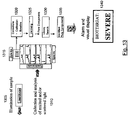
A feature of the ultra compact filter is that the optical properties and Raman features inherent to PMMA do not substantially degrade the Raman detection of bio-threat agents. FIG. 15 shows the Raman spectrum of PMMA collected using high performance microscope glass optics. FIG. 15 also shows the Raman spectrum of a species of Anthrax (BG) collected with the same optics. Finally, FIG. 15 shows a Raman spectrum of BG after introducing a thin plate of PMMA into the laser illumination and collection optical paths. So long as the PMMA is located in an optical region where the light rays are parallel, it does not introduce significant background into the measured spectrum. That is, PMMA is illumination optical path does not prevent collection of BG Raman spectrum. The contribution to the Raman spectrum attributable to PMMA can be also be used as an internal calibrant (intensity and wavelength) which can assist automated correction of instrument response and overall improved performance of a fielded system. Instrument calibration enables compensation of instrument variation including laser line drift and quantitative analysis.
The following Table shows non-exclusive and exemplary specifications for an embodiment of the compact imaging spectrometer.
| Performance Parameter | Specification |
| Laser excitation wavelength | 532 nm; <0.2 nm |
| and bandwidth: | |
| Imaging aperture: | 0.5″ or larger |
| Field of view (angular | +/−3 degrees |
| incidence): | |
| Free spectral range: | 500-750 nm |
| Usable Raman range: | 350-3,200 cm−1 |
| Resolution: | 0.25 nm FWHM @ 500 nm, <10 cm−1 |
| Off-peak rejection: | 10,000:1 total energy |
| Transmission: | min 30% |
Although the disclosure is described using illustrative embodiments provided herein, it should be understood that the principles of the disclosure are not limited hereto and may include modification thereto and permutations thereof.
Claims (45)
1. A portable system for obtaining a two dimensional image of a sample having a first and a second spatial dimension, comprising:
a photon emission source for sequentially illuminating a portion of said sample with a plurality of photons to thereby produce photons scattered by the sample wherein the photon emission source illuminates said sample along the first spatial dimension for each of plural predetermined positions of the second spatial dimension;
an optical lens for collecting the scattered photons to produce therefrom filtered photons;
a dispersive spectrometer for determining a wavelength of ones of the filtered photons;
a photon detector for receiving the filtered photons and obtaining therefrom a spectrum of said sample; and
a processor for producing a two dimensional image of said sample which includes information from said spectrum.
2. The system of claim 1 wherein said photon detector is selected from the group consisting of: charge-coupled device, complementary metal oxide semiconductor, charge injection device, intensified charge injection device, electron multiplying charge-coupled device, silicon photo diode, silicon avalanche diode, and focal plane array.
3. The system of claim 1 wherein said photon emission source is a laser.
4. The system of claim 1 wherein said photon emission source is a light emitting diode.
5. The system of claim 4 wherein said light emitting diode is disposed as a ring.
6. The system of claim 5 wherein said light emitting diode is a plurality of light emitting diodes.
7. The system of claim 4 wherein said light emitting diode is a plurality of light emitting diodes wherein one of said plural light emitting diodes emits photons at a wavelength that is different than a wavelength of photons emitted by another of said plural light emitting diodes.
8. The system of claim 7 wherein the wavelength of photons emitted by one of said plural light emitting diodes is in the ultraviolet wavelength range.
9. The system of claim 7 wherein the wavelength of photons emitted by one of said plural light emitting diodes is in the near infrared wavelength range.
10. The system of claim 1 wherein said spectrum is obtained over a predetermined period of time and said sample is stationary during said predetermined period of time.
11. The system of claim 1 wherein said scattered photons include photons emitted by said sample.
12. The system of claim 1 wherein said spectrum is a Raman spectrum.
13. The system of claim 1 wherein the system is a hand-held system.
14. The system of claim 1 wherein said optical lens includes a laser rejection filter.
15. The system of claim 1 wherein said spectrum is a fluorescence spectrum.
16. The system of claim 1 wherein said spectrum is a near infrared spectrum.
17. A method for obtaining a two dimensional image of a sample using a hand-held device, the method comprising the steps of:
providing a sample having a first and a second spatial dimension;
sequentially illuminating a portion of said sample with a plurality of photons from a photon emission source to thereby produce photons scattered by the sample the sequential illumination occurring alone the first spatial dimension for each of plural predetermined positions of the second spatial dimension;
collecting the scattered photons and producing therefrom filtered photons;
determining a wavelength of ones of the filtered photons;
receiving the filtered photons in a photon detector and obtaining therefrom a spectrum of said sample; and
processing the spectra and producing therefrom a two dimensional image of said sample which includes information from said spectrum.
18. The method of claim 17 wherein the step of illuminating the sample is accomplished by illuminating the sample with plural light emitting diodes wherein one of said plural light emitting diodes emits photons at a wavelength that is different than a wavelength of photons emitted by another of said plural light emitting diodes.
19. The method of claim 18 wherein the wavelength of photons emitted by one of said plural light emitting diodes is in the ultraviolet wavelength range.
20. The method of claim 18 wherein the wavelength of photons emitted by one of said plural light emitting diodes is in the near infrared wavelength range.
21. The method of claim 17 wherein the step of obtaining the spectrum is obtained over a predetermined period of time and said sample is stationary during said predetermined period of time.
22. A portable system for obtaining a spatially accurate wavelength-resolved image of a sample having a first and a second spatial dimension, comprising:
a photon emission source for sequentially illuminating a portion of said sample with a plurality of photons to thereby produce photons emitted by the sample wherein the photon emission source illuminates said sample along the first spatial dimension for each of plural predetermined positions of the second spatial dimension;
an optical lens for collecting the emitted photons and producing therefrom filtered photons;
a dispersive spectrometer for determining a wavelength of ones of the filtered photons; and
a photon detector for receiving the filtered photons and obtaining therefrom a spectrum of said sample.
23. The system of claim 22 wherein the photon emission source illuminates the sample along the first spatial dimension for each of plural predetermined positions of the second spatial dimension to thereby obtain plural spectra of said sample.
24. The system of claim 23 including a processor for producing a two dimensional image of said sample from the plural spectra.
25. The system of claim 22 wherein said photon detector is selected from the group consisting of: charge-coupled device, complementary metal oxide semiconductor, charge injection device, intensified charge injection device, electron multiplying charge-coupled device, silicon photo diode, silicon avalanche diode, and focal plane array.
26. The system of claim 22 wherein said photon emission source is a laser.
27. The system of claim 22 wherein said photon emission source is a light emitting diode.
28. The system of claim 27 wherein said light emitting diode is disposed as a ring.
29. The system of claim 28 wherein said light emitting diode is a plurality of light emitting diodes.
30. The system of claim 27 wherein said light emitting diode is a plurality of light emitting diodes wherein one of said plural light emitting diodes emits photons at a wavelength that is different than a wavelength of photons emitted by another of said plural light emitting diodes.
31. The system of claim 30 wherein the wavelength of photons emitted by one of said plural light emitting diodes is in the ultraviolet wavelength range.
32. The system of claim 30 wherein the wavelength of photons emitted by one of said plural light emitting diodes is in the near infrared wavelength range.
33. The system of claim 22 wherein said spectrum is obtained over a predetermined period of time and said sample is stationary during said predetermined period of time.
34. The system of claim 22 wherein said spectrum is a Raman spectrum.
35. The system of claim 22 wherein the system is a hand-held system.
36. The system of claim 22 wherein said optical lens includes a laser rejection filter.
37. The system of claim 22 wherein said spectrum is a fluorescence spectrum.
38. The system of claim 22 wherein said spectrum is a near infrared spectrum.
39. A method for obtaining a spatially accurate wavelength-resolved image of a sample using a hand-held device, the method comprising the steps of:
providing a sample having a first and a second spatial dimension;
sequentially illuminating a portion of said sample with a plurality of photons from a photon emission source to thereby produce photons scattered by the sample the sequential illumination occurring along the first spatial dimension for each of plural predetermined positions of the second spatial dimension;
collecting the scattered photons and producing therefrom filtered photons;
determining a wavelength of ones of the filtered photons; and
receiving the filtered photons in a photon detector and obtaining therefrom a spectrum of said sample.
40. The method of claim 39 wherein the sample is illuminated along the first spatial dimension for each of plural predetermined positions of the second spatial dimension to thereby obtain plural spectra of said sample.
41. The method of claim 40 including the step of processing the spectra and producing therefrom a two dimensional image of said sample.
42. The method of claim 39 wherein the step of illuminating the sample is accomplished by illuminating the sample with plural light emitting diodes wherein one of said plural light emitting diodes emits photons at a wavelength that is different than a wavelength of photons emitted by another of said plural light emitting diodes.
43. The method of claim 42 wherein the wavelength of photons emitted by one of said plural light emitting diodes is in the ultraviolet wavelength range.
44. The method of claim 42 wherein the wavelength of photons emitted by one of said plural light emitting diodes is in the near infrared wavelength range.
45. The method of claim 39 wherein the step of obtaining the spectrum is obtained over a predetermined period of time and said sample is stationary during said predetermined period of time.
Priority Applications (1)
| Application Number | Priority Date | Filing Date | Title |
|---|---|---|---|
| US11/364,180 US7307705B2 (en) | 2003-07-18 | 2006-03-01 | Method and apparatus for compact dispersive imaging spectrometer |
Applications Claiming Priority (3)
| Application Number | Priority Date | Filing Date | Title |
|---|---|---|---|
| US48824603P | 2003-07-18 | 2003-07-18 | |
| US10/893,339 US7084972B2 (en) | 2003-07-18 | 2004-07-19 | Method and apparatus for compact dispersive imaging spectrometer |
| US11/364,180 US7307705B2 (en) | 2003-07-18 | 2006-03-01 | Method and apparatus for compact dispersive imaging spectrometer |
Related Parent Applications (1)
| Application Number | Title | Priority Date | Filing Date |
|---|---|---|---|
| US10/893,339 Continuation US7084972B2 (en) | 2003-07-18 | 2004-07-19 | Method and apparatus for compact dispersive imaging spectrometer |
Publications (2)
| Publication Number | Publication Date |
|---|---|
| US20060146315A1 US20060146315A1 (en) | 2006-07-06 |
| US7307705B2 true US7307705B2 (en) | 2007-12-11 |
Family
ID=34079410
Family Applications (6)
| Application Number | Title | Priority Date | Filing Date |
|---|---|---|---|
| US10/893,339 Active US7084972B2 (en) | 2003-07-18 | 2004-07-19 | Method and apparatus for compact dispersive imaging spectrometer |
| US10/893,230 Active US6985233B2 (en) | 2003-07-18 | 2004-07-19 | Method and apparatus for compact Fabry-Perot imaging spectrometer |
| US10/893,332 Active 2025-01-24 US7012695B2 (en) | 2003-07-18 | 2004-07-19 | Method and apparatus for multiwavelength imaging spectrometer |
| US10/893,331 Expired - Fee Related US6985216B2 (en) | 2003-07-18 | 2004-07-19 | Method and apparatus for compact birefringent interference imaging spectrometer |
| US11/216,175 Active US7262839B2 (en) | 2003-07-18 | 2005-09-01 | Method and apparatus for compact birefringent interference imaging spectrometer |
| US11/364,180 Active US7307705B2 (en) | 2003-07-18 | 2006-03-01 | Method and apparatus for compact dispersive imaging spectrometer |
Family Applications Before (5)
| Application Number | Title | Priority Date | Filing Date |
|---|---|---|---|
| US10/893,339 Active US7084972B2 (en) | 2003-07-18 | 2004-07-19 | Method and apparatus for compact dispersive imaging spectrometer |
| US10/893,230 Active US6985233B2 (en) | 2003-07-18 | 2004-07-19 | Method and apparatus for compact Fabry-Perot imaging spectrometer |
| US10/893,332 Active 2025-01-24 US7012695B2 (en) | 2003-07-18 | 2004-07-19 | Method and apparatus for multiwavelength imaging spectrometer |
| US10/893,331 Expired - Fee Related US6985216B2 (en) | 2003-07-18 | 2004-07-19 | Method and apparatus for compact birefringent interference imaging spectrometer |
| US11/216,175 Active US7262839B2 (en) | 2003-07-18 | 2005-09-01 | Method and apparatus for compact birefringent interference imaging spectrometer |
Country Status (6)
| Country | Link |
|---|---|
| US (6) | US7084972B2 (en) |
| EP (1) | EP1646841A4 (en) |
| JP (1) | JP2006528353A (en) |
| CN (1) | CN100437020C (en) |
| CA (1) | CA2532949A1 (en) |
| WO (4) | WO2005008200A2 (en) |
Cited By (9)
| Publication number | Priority date | Publication date | Assignee | Title |
|---|---|---|---|---|
| US20110101242A1 (en) * | 2008-07-07 | 2011-05-05 | Jason Dickens | Methods, apparatus and systems employing multiple energy sources for analyzing compositions |
| US8379193B2 (en) | 2008-08-27 | 2013-02-19 | Chemimage Corporation | SWIR targeted agile raman (STAR) system for on-the-move detection of emplace explosives |
| US8743358B2 (en) | 2011-11-10 | 2014-06-03 | Chemimage Corporation | System and method for safer detection of unknown materials using dual polarized hyperspectral imaging and Raman spectroscopy |
| US8994934B1 (en) | 2010-11-10 | 2015-03-31 | Chemimage Corporation | System and method for eye safe detection of unknown targets |
| US9052290B2 (en) | 2012-10-15 | 2015-06-09 | Chemimage Corporation | SWIR targeted agile raman system for detection of unknown materials using dual polarization |
| US9182351B2 (en) | 2013-11-26 | 2015-11-10 | Nanometrics Incorporated | Optical metrology system for spectral imaging of a sample |
| US9846122B2 (en) | 2013-11-26 | 2017-12-19 | Nanometrics Incorporated | Optical metrology system for spectral imaging of a sample |
| RU2692825C2 (en) * | 2017-10-23 | 2019-06-28 | Ирлан Витальевич Шабельников | Method of spectral laser scanning of composite materials in accordance with optical density of its matrix and composite components |
| RU211810U1 (en) * | 2022-03-04 | 2022-06-23 | Роман Петрович Медведев | DEVICE FOR SPECTRAL LASER SCANNING OF MATERIALS |
Families Citing this family (178)
| Publication number | Priority date | Publication date | Assignee | Title |
|---|---|---|---|---|
| NL1023679C2 (en) * | 2003-06-17 | 2004-12-20 | Tno | Light-emitting diode. |
| US7542138B2 (en) * | 2003-07-18 | 2009-06-02 | Chemimage Corporation | Sample container and system for a handheld spectrometer and method for using therefor |
| WO2005008200A2 (en) * | 2003-07-18 | 2005-01-27 | Chemimage Corporation | Method and apparatus for compact dispersive imaging spectrometer |
| US7286222B2 (en) * | 2003-07-18 | 2007-10-23 | Chemimage Corporation | Sample container and system for a handheld spectrometer and method for using therefor |
| US7738095B2 (en) * | 2003-07-18 | 2010-06-15 | Chemimage Corporation | Method and apparatus for compact spectrometer for detecting hazardous agents |
| CN1875528B (en) * | 2003-09-03 | 2010-09-29 | 宾奥普迪克斯股份有限公司 | Single longitudinal mode laser diode |
| JP3770326B2 (en) * | 2003-10-01 | 2006-04-26 | セイコーエプソン株式会社 | Analysis equipment |
| WO2005121724A2 (en) * | 2004-01-21 | 2005-12-22 | Optical Insights, Llc | Method and apparatus for multi-mode spectral imaging |
| JP2005316650A (en) * | 2004-04-28 | 2005-11-10 | Sony Corp | Communication terminal and content selection presentation method |
| US9442070B1 (en) | 2004-10-05 | 2016-09-13 | Photon Systems, Inc. | Native fluorescence detection methods, devices, and systems for organic compounds |
| US7590161B1 (en) * | 2004-10-05 | 2009-09-15 | Photon Systems | Electron beam pumped semiconductor laser |
| US8759791B1 (en) | 2004-10-05 | 2014-06-24 | Photon Systems, Inc. | Native fluorescence detection methods and detectors for naphthalene and/or other volatile organic compound vapors |
| US8548570B2 (en) | 2004-11-29 | 2013-10-01 | Hypermed Imaging, Inc. | Hyperspectral imaging of angiogenesis |
| JP5149015B2 (en) * | 2004-12-28 | 2013-02-20 | ハイパーメツド・イメージング・インコーポレイテツド | Hyperspectral / multispectral imaging in the determination, evaluation and monitoring of systemic physiology and shock |
| AU2013202796B2 (en) * | 2004-12-28 | 2016-06-09 | Hypermed Imaging, Inc. | Hyperspectral/multispectral imaging in determination, assessment and monitoring of systemic physiology and shock |
| CA2586476C (en) * | 2005-01-31 | 2009-06-30 | Chemimage Corporation | Apparatus and method for chemical imaging of a biological sample |
| US7400405B2 (en) * | 2005-02-18 | 2008-07-15 | Bio-Chek Llc | Pesticide detector and method |
| US7385704B2 (en) * | 2005-03-30 | 2008-06-10 | Xerox Corporation | Two-dimensional spectral cameras and methods for capturing spectral information using two-dimensional spectral cameras |
| WO2006107947A2 (en) | 2005-04-04 | 2006-10-12 | Hypermed, Inc. | Hyperspectral imaging in diabetes and peripheral vascular disease |
| JP2008536116A (en) * | 2005-04-08 | 2008-09-04 | ケミマジ コーポレーション | System and method for chemical imaging of microarrays |
| US7473884B2 (en) * | 2005-04-21 | 2009-01-06 | Avago Technologies Ecbu Ip (Singapore) Pte. Ltd. | Orientation determination utilizing a cordless device |
| US7609249B2 (en) * | 2005-04-21 | 2009-10-27 | Avago Technologies Ecbu Ip (Singapore) Pte. Ltd. | Position determination utilizing a cordless device |
| WO2006116637A2 (en) * | 2005-04-27 | 2006-11-02 | Massachusetts Institute Of Technology | Raman spectroscopy for non-invasive glucose measurements |
| US7420663B2 (en) * | 2005-05-24 | 2008-09-02 | Bwt Property Inc. | Spectroscopic sensor on mobile phone |
| EP1902301A4 (en) | 2005-07-14 | 2010-09-22 | Chemimage Corp | Time and space resolved standoff hyperspectral ied explosives lidar detector |
| US8582089B2 (en) * | 2006-06-09 | 2013-11-12 | Chemimage Corporation | System and method for combined raman, SWIR and LIBS detection |
| US9103793B2 (en) * | 2005-07-22 | 2015-08-11 | Massachusetts Institute Of Technology | Intrinsic Raman spectroscopy |
| WO2007016682A2 (en) * | 2005-08-02 | 2007-02-08 | Kla-Tencor Technologies Corporation | Systems configured to generate output corresponding to defects on a specimen |
| WO2007038410A2 (en) * | 2005-09-27 | 2007-04-05 | Chemimage Corporation | Liquid crystal filter with tunable rejection band |
| US7561274B2 (en) * | 2005-10-20 | 2009-07-14 | Duke University | Optical spectroscopy utilizing planar spectral filters |
| US7760197B2 (en) * | 2005-10-31 | 2010-07-20 | Hewlett-Packard Development Company, L.P. | Fabry-perot interferometric MEMS electromagnetic wave modulator with zero-electric field |
| US20070109527A1 (en) * | 2005-11-14 | 2007-05-17 | Wenstrand John S | System and method for generating position information |
| US20070145258A1 (en) * | 2005-12-16 | 2007-06-28 | Nelson Matthew P | Method and apparatus for automated spectral calibration |
| US7859753B2 (en) * | 2005-12-21 | 2010-12-28 | Chem Image Corporation | Optical birefringence filters with interleaved absorptive and zero degree reflective polarizers |
| US8368880B2 (en) * | 2005-12-23 | 2013-02-05 | Chemimage Corporation | Chemical imaging explosives (CHIMED) optical sensor using SWIR |
| US7355714B2 (en) * | 2005-12-29 | 2008-04-08 | Xerox Corporation | Reconfigurable MEMS fabry-perot tunable matrix filter systems and methods |
| US7417746B2 (en) * | 2005-12-29 | 2008-08-26 | Xerox Corporation | Fabry-perot tunable filter systems and methods |
| WO2007082202A2 (en) * | 2006-01-09 | 2007-07-19 | Chemimage Corporation | Birefringent spectral filter with wide field of view and associated communications method and apparatus |
| WO2007117764A2 (en) * | 2006-02-13 | 2007-10-18 | Chemimage Corporation | System and method for super resolution of a sample in a fiber array spectral translator system |
| US8140500B2 (en) * | 2006-03-17 | 2012-03-20 | Thermo Electron Scientific Instruments Llc | Spectral measurement with assisted data analysis |
| US7796119B2 (en) * | 2006-04-03 | 2010-09-14 | Avago Technologies General Ip (Singapore) Pte. Ltd. | Position determination with reference |
| US20070236757A1 (en) * | 2006-04-10 | 2007-10-11 | Duncan Stewart | Rich color image processing method and apparatus |
| US7505128B2 (en) * | 2006-04-10 | 2009-03-17 | General Electric Company | Compact, hand-held raman spectrometer microsystem on a chip |
| JP5123492B2 (en) * | 2006-05-22 | 2013-01-23 | オリンパス株式会社 | Optical device for spectral image observation |
| FI119830B (en) * | 2006-05-24 | 2009-03-31 | Valtion Teknillinen | Spectrometer and interferometric procedure |
| US20070279627A1 (en) * | 2006-06-02 | 2007-12-06 | Tack Leslie M | Raman instrumentation |
| US7796269B2 (en) * | 2006-06-06 | 2010-09-14 | Morpho Detection, Inc. | Irregularly shaped actuator fingers for a micro-electromechanical system fabry-perot filter |
| US7551287B2 (en) * | 2006-06-06 | 2009-06-23 | Ge Homeland Protection, Inc. | Actuator for micro-electromechanical system fabry-perot filter |
| US20100220331A1 (en) * | 2006-06-06 | 2010-09-02 | Anis Zribi | Micro-electromechanical system fabry-perot filter cavity |
| US7573578B2 (en) * | 2006-06-06 | 2009-08-11 | Ge Homeland Protection, Inc. | Micro-electromechanical system Fabry-Perot filter mirrors |
| US20110237446A1 (en) * | 2006-06-09 | 2011-09-29 | Chemlmage Corporation | Detection of Pathogenic Microorganisms Using Fused Raman, SWIR and LIBS Sensor Data |
| WO2008016590A2 (en) | 2006-07-31 | 2008-02-07 | Visualant, Inc. | System and method of evaluating an object using electromagnetic energy |
| US7996173B2 (en) * | 2006-07-31 | 2011-08-09 | Visualant, Inc. | Method, apparatus, and article to facilitate distributed evaluation of objects using electromagnetic energy |
| US8081304B2 (en) * | 2006-07-31 | 2011-12-20 | Visualant, Inc. | Method, apparatus, and article to facilitate evaluation of objects using electromagnetic energy |
| US8164061B2 (en) * | 2006-09-13 | 2012-04-24 | Delphi Technologies, Inc. | Method and apparatus for a universal infrared analyzer |
| US7583418B2 (en) * | 2006-09-26 | 2009-09-01 | Xerox Corporation | Array based sensor to measure single separation or mixed color (or IOI) patches on the photoreceptor using MEMS based hyperspectral imaging technology |
| US7623278B2 (en) * | 2006-09-26 | 2009-11-24 | Xerox Corporation | MEMS Fabry-Perot inline color scanner for printing applications using stationary membranes |
| US7417796B2 (en) * | 2006-09-29 | 2008-08-26 | Chemimage Corporation | Wavelength discrimination filter for infrared wavelengths |
| WO2008042766A1 (en) * | 2006-09-29 | 2008-04-10 | Chemimage Corporation | Spectral imaging system |
| ES2323204B2 (en) * | 2006-10-06 | 2010-02-15 | Universidade De Santiago De Compostela | IMAGE SPECTROMETER AND IMAGE SPECTROSCOPY METHOD. |
| US20080100839A1 (en) * | 2006-10-31 | 2008-05-01 | Fouquet Julie E | Method and system for measuring light propagating at multiple wavelengths |
| US20080144013A1 (en) * | 2006-12-01 | 2008-06-19 | Institute For Technology Development | System and method for co-registered hyperspectral imaging |
| US20080192889A1 (en) * | 2007-02-14 | 2008-08-14 | Martin Rohde | Handheld x-ray fluorescence spectrometer |
| WO2008103937A2 (en) * | 2007-02-23 | 2008-08-28 | Thermo Niton Analyzers Llc | Hand-held, self-contained optical emission spectroscopy (oes) analyzer |
| US8717572B2 (en) * | 2007-06-12 | 2014-05-06 | Hewlett-Packard Development Company, L.P. | Spectrophotometer |
| WO2009012352A1 (en) * | 2007-07-18 | 2009-01-22 | Bruker Biosciences Corporation | Handheld spectrometer including wireless capabilities |
| US7626696B2 (en) * | 2007-08-07 | 2009-12-01 | Chemimage Corporation | Method and apparatus for reconfigurable field of view in a FAST-based imaging system |
| DE202008003977U1 (en) * | 2008-02-26 | 2009-07-02 | Bürkert Werke GmbH & Co. KG | microspectrometer |
| US20090231677A1 (en) * | 2008-03-13 | 2009-09-17 | Usa As Represented By The Administrator Of The National Aeronautics And Space Administration | Variable Focal Point Optical Assembly Using Zone Plate and Electro-Optic Material |
| US7844145B1 (en) * | 2008-04-14 | 2010-11-30 | The United States Of America As Represented By The Secretary Of The Navy | MEMS-based multi-channel Fabry-Perot interferometer system with increased tuning range and resolution |
| US8094306B2 (en) * | 2008-08-15 | 2012-01-10 | The United States Of America As Represented By The Administrator Of The National Aeronautics And Space Administration | Micro ring grating spectrometer with adjustable aperture |
| US8174695B2 (en) * | 2008-08-15 | 2012-05-08 | The United States Of America As Represented By The Administrator Of The National Aeronautics And Space Administration | Arrayed micro-ring spectrometer system and method of use |
| US8018815B2 (en) * | 2008-08-15 | 2011-09-13 | The United States Of America As Represented By The Administrator Of The National Aeronautics And Space Administration | Micro-Fresnel zone plate optical devices using densely accumulated ray points |
| US8059273B2 (en) * | 2008-08-15 | 2011-11-15 | The United States Of America As Represented By The Administrator Of The National Aeronautics And Space Administration | Micro spectrometer for parallel light and method of use |
| GB0818822D0 (en) * | 2008-10-14 | 2008-11-19 | Edinburgh Instr | Reduction of stray light |
| EP2177747A1 (en) * | 2008-10-15 | 2010-04-21 | Continental Automotive GmbH | Injection valve and method for its manufacturing |
| US8440959B2 (en) * | 2008-11-18 | 2013-05-14 | Chemimage Corporation | Method and apparatus for automated spectral calibration |
| US10598596B1 (en) | 2008-11-28 | 2020-03-24 | Photon Systems, Inc. | Native fluorescence detection methods, devices, and systems for organic compounds |
| US10753863B1 (en) | 2008-11-28 | 2020-08-25 | Photon Systems, Inc. | Spectroscopic chemical analysis methods and apparatus |
| WO2010076806A1 (en) * | 2009-01-01 | 2010-07-08 | Metal Power Analytical (India) P. Ltd | High resolution optical spectrograph |
| US7978346B1 (en) * | 2009-02-18 | 2011-07-12 | University Of Central Florida Research Foundation, Inc. | Methods and systems for realizing high resolution three-dimensional optical imaging |
| CN101526397B (en) * | 2009-03-27 | 2011-03-23 | 福州高意光学有限公司 | Spectrometer |
| US8886206B2 (en) | 2009-05-01 | 2014-11-11 | Digimarc Corporation | Methods and systems for content processing |
| US9749607B2 (en) | 2009-07-16 | 2017-08-29 | Digimarc Corporation | Coordinated illumination and image signal capture for enhanced signal detection |
| US9103714B2 (en) * | 2009-10-06 | 2015-08-11 | Chemimage Corporation | System and methods for explosives detection using SWIR |
| US9664563B2 (en) | 2009-12-02 | 2017-05-30 | University Of Hawaii | Fabry-perot fourier transform spectrometer |
| JP5170582B2 (en) * | 2010-04-05 | 2013-03-27 | 横河電機株式会社 | Spectroscopic analyzer for microscope |
| US8400574B2 (en) | 2010-04-16 | 2013-03-19 | Chemimage Corporation | Short wave infrared multi-conjugate liquid crystal tunable filter |
| JP5668345B2 (en) * | 2010-07-13 | 2015-02-12 | セイコーエプソン株式会社 | Optical filter, optical filter module, spectrophotometer and optical instrument |
| US8815156B2 (en) | 2010-07-19 | 2014-08-26 | Andalyze, Inc. | Sensor housing and reagent chemistry |
| WO2012012174A1 (en) * | 2010-07-19 | 2012-01-26 | Andalyze, Inc. | Sensor housing and reagent chemistry |
| US8951472B2 (en) | 2010-07-19 | 2015-02-10 | Andalyze, Inc. | Portable fluorimetric apparatus, method and system |
| KR101184273B1 (en) | 2010-11-15 | 2012-09-21 | 길 원 윤 | Separating type spectrophotometer |
| WO2012070314A1 (en) * | 2010-11-22 | 2012-05-31 | 横河電機株式会社 | Microscope spectrometer, optical axis shift correction device, spectroscope and microscope using same |
| JP5720200B2 (en) * | 2010-11-25 | 2015-05-20 | セイコーエプソン株式会社 | Optical module and optical measuring device |
| US8736777B2 (en) | 2011-01-19 | 2014-05-27 | Chemimage Technologies Llc | VIS-SNIR multi-conjugate liquid crystal tunable filter |
| US9256013B2 (en) | 2011-04-14 | 2016-02-09 | Chemimage Technologies Llc | Short-wavelength infrared (SWIR) multi-conjugate liquid crystal tunable filter |
| PT2564154E (en) * | 2011-05-02 | 2013-12-05 | Foss Analytical As | Spectrometric instrument |
| JP5743715B2 (en) * | 2011-05-26 | 2015-07-01 | キヤノン株式会社 | Acoustic signal receiver |
| US9060110B2 (en) | 2011-10-07 | 2015-06-16 | Canon Kabushiki Kaisha | Image capture with tunable polarization and tunable spectral sensitivity |
| DE102011084348A1 (en) * | 2011-10-12 | 2013-04-18 | Carl Zeiss Microscopy Gmbh | Miniaturized opto-electronic system for spectral analysis |
| CN104040309B (en) * | 2011-11-03 | 2019-06-07 | 威利食品有限公司 | Inexpensive spectrometric system for end user's food analysis |
| WO2013119824A1 (en) | 2012-02-10 | 2013-08-15 | Visualant, Inc. | Systems, methods and articles related to machine-readable indicia and symbols |
| JP2013181912A (en) * | 2012-03-02 | 2013-09-12 | Seiko Epson Corp | Component analyzer |
| CN103364386B (en) * | 2012-03-27 | 2016-04-06 | 武汉鹰飞拓光电子有限公司 | Deep ultraviolet laser Raman spectrometer |
| US9593982B2 (en) | 2012-05-21 | 2017-03-14 | Digimarc Corporation | Sensor-synchronized spectrally-structured-light imaging |
| US9060113B2 (en) | 2012-05-21 | 2015-06-16 | Digimarc Corporation | Sensor-synchronized spectrally-structured-light imaging |
| CN102854618A (en) * | 2012-06-21 | 2013-01-02 | 浙江师范大学 | Optical filter with variable and adjustable bandwidth and wavelength |
| CN104661594B (en) * | 2012-06-28 | 2017-10-13 | 迅捷有限责任公司 | The device infrared measurement apparatus of intelligent movable, π methods and the system for analyzing material |
| KR101904718B1 (en) * | 2012-08-27 | 2018-10-05 | 삼성전자주식회사 | Apparatus and method for capturing color images and depth images |
| JP5429698B2 (en) * | 2012-11-08 | 2014-02-26 | 横河電機株式会社 | Spectroscopic analyzer for microscope and spectroscopic analysis method of spectroscopic analyzer for microscope |
| KR20140063159A (en) * | 2012-11-16 | 2014-05-27 | 삼성전기주식회사 | Measurement device of degree of cure |
| US20140231626A1 (en) * | 2012-11-26 | 2014-08-21 | Chemlmage Corporation | System and method for detecting target materials using a vis-nir detector |
| US9316581B2 (en) | 2013-02-04 | 2016-04-19 | Visualant, Inc. | Method, apparatus, and article to facilitate evaluation of substances using electromagnetic energy |
| US9041920B2 (en) | 2013-02-21 | 2015-05-26 | Visualant, Inc. | Device for evaluation of fluids using electromagnetic energy |
| CN103162828B (en) * | 2013-02-26 | 2015-10-21 | 浙江大学 | Based on the ultrahigh resolution spectrometer of tunable enamel Pohle-perot filter and array type detector spectrometer |
| US20140253921A1 (en) * | 2013-03-07 | 2014-09-11 | Qiushui Chen | Spectroscopic systems and methods |
| US9664610B2 (en) | 2013-03-12 | 2017-05-30 | Visualant, Inc. | Systems for fluid analysis using electromagnetic energy that is reflected a number of times through a fluid contained within a reflective chamber |
| US20140378810A1 (en) | 2013-04-18 | 2014-12-25 | Digimarc Corporation | Physiologic data acquisition and analysis |
| CN103323410A (en) * | 2013-05-24 | 2013-09-25 | 暨南大学 | A device and a method based on a liquid-crystal filtering device for microscopic spectral imaging |
| US9621760B2 (en) | 2013-06-07 | 2017-04-11 | Digimarc Corporation | Information coding and decoding in spectral differences |
| FR3007139B1 (en) * | 2013-06-14 | 2016-11-11 | Axens | DEVICE AND METHOD FOR ANALYZING THE DRIVING OF SIMPLE MOBILE BED XYLENE SEPARATION UNITS USING A RAMAN SPECTROMETER |
| KR20160023838A (en) | 2013-06-24 | 2016-03-03 | 테크놀로지 이노베이션 모멘텀 펀드 (이스라엘) 리미티드 파트너쉽 | A system and method for color image acquisition |
| GB2529070B (en) | 2013-08-02 | 2017-07-12 | Verifood Ltd | Spectrometer comprising a plurality of isolated optical paths |
| WO2015101992A2 (en) | 2014-01-03 | 2015-07-09 | Verifood, Ltd. | Spectrometry systems, methods, and applications |
| US9253420B2 (en) * | 2014-02-12 | 2016-02-02 | Xerox Corporation | Hyperspectral single pixel imager with fabry perot filter |
| DE102014105222A1 (en) * | 2014-04-11 | 2015-10-15 | Jenoptik Optical Systems Gmbh | Camera with integrated spectrometer |
| US10113910B2 (en) | 2014-08-26 | 2018-10-30 | Digimarc Corporation | Sensor-synchronized spectrally-structured-light imaging |
| US9752935B2 (en) * | 2014-08-29 | 2017-09-05 | Marqmetrix, Inc. | Portable analytical equipment |
| WO2016063284A2 (en) | 2014-10-23 | 2016-04-28 | Verifood, Ltd. | Accessories for handheld spectrometer |
| US9677935B2 (en) * | 2014-11-03 | 2017-06-13 | Trutag Technologies, Inc. | Fabry-perot spectral image measurement |
| US9727941B1 (en) | 2014-11-19 | 2017-08-08 | Digimarc Corporation | Optimizing optical scanners for digital watermark detection |
| WO2016111308A1 (en) * | 2015-01-07 | 2016-07-14 | 平本 政夫 | Multi-spectrum image pickup device |
| US10048130B2 (en) * | 2015-01-09 | 2018-08-14 | California Institute Of Technology | Context imaging raman spectrometer |
| US10746600B2 (en) * | 2015-01-09 | 2020-08-18 | California Institute Of Technology | Dual wavelength context imaging Raman and fluorescence spectrometer |
| WO2016125165A2 (en) | 2015-02-05 | 2016-08-11 | Verifood, Ltd. | Spectrometry system with visible aiming beam |
| WO2016125164A2 (en) | 2015-02-05 | 2016-08-11 | Verifood, Ltd. | Spectrometry system applications |
| SG10201501196PA (en) | 2015-02-16 | 2016-09-29 | Lighthaus Photonics Pte Ltd | Compact spectrometer |
| US9316539B1 (en) | 2015-03-10 | 2016-04-19 | LightHaus Photonics Pte. Ltd. | Compact spectrometer |
| US10066990B2 (en) | 2015-07-09 | 2018-09-04 | Verifood, Ltd. | Spatially variable filter systems and methods |
| JP7046792B2 (en) | 2015-07-15 | 2022-04-04 | テクノロジー イノベーション モメンタム ファンド(イスラエル)リミテッド パートナーシップ | Adjustable MEMS Etalon |
| US10605660B2 (en) | 2015-07-30 | 2020-03-31 | Technology Innovation Momentum Fund (Israel) Limited Partnership | Spectral imaging method and system |
| US11656180B2 (en) | 2015-08-03 | 2023-05-23 | Ysi, Inc. | Multi excitation-multi emission fluorometer for multiparameter water quality monitoring |
| US10203246B2 (en) | 2015-11-20 | 2019-02-12 | Verifood, Ltd. | Systems and methods for calibration of a handheld spectrometer |
| US9857223B2 (en) | 2015-11-20 | 2018-01-02 | Raytheon Company | Proximity focus imaging interferometer |
| TWI579540B (en) | 2015-12-02 | 2017-04-21 | 財團法人工業技術研究院 | Multi-point spectral system |
| KR101847247B1 (en) * | 2015-12-08 | 2018-04-10 | 한양대학교 산학협력단 | Sensing system based on fourier domain mode locked tunable laser |
| KR101857856B1 (en) * | 2015-12-15 | 2018-05-15 | 한국과학기술원 | Method for oam multi-mode transmission by rf lens antenna |
| CN105444883A (en) * | 2015-12-22 | 2016-03-30 | 武汉麦视威光电科技有限公司 | Imaging spectrometer based on liquid crystal tunable optical filter and full spectrum range automatic acquiring method |
| JP2017150856A (en) * | 2016-02-22 | 2017-08-31 | 旭化成エレクトロニクス株式会社 | Measurement device, sensor device, and portable terminal |
| JP2016130743A (en) * | 2016-04-19 | 2016-07-21 | セイコーエプソン株式会社 | Spectroscopic measuring apparatus |
| FR3050831B1 (en) * | 2016-04-29 | 2018-04-27 | Silios Technologies | MULTISPECTRAL IMAGING DEVICE |
| EP3488204A4 (en) | 2016-07-20 | 2020-07-22 | Verifood Ltd. | Accessories for handheld spectrometer |
| US10791933B2 (en) | 2016-07-27 | 2020-10-06 | Verifood, Ltd. | Spectrometry systems, methods, and applications |
| US10768497B2 (en) * | 2016-10-03 | 2020-09-08 | Xerox Corporation | Hyperspectral imaging system |
| KR20180056277A (en) | 2016-11-18 | 2018-05-28 | 삼성전자주식회사 | Spectrometer and spectrometer module |
| EP3542149A4 (en) * | 2016-11-20 | 2020-05-20 | Unispectral Ltd. | Multi-band imaging systems |
| US20180181791A1 (en) * | 2016-12-28 | 2018-06-28 | Intel Corporation | Spectral signature assisted finger associated user application |
| CN106802184B (en) * | 2017-02-22 | 2019-03-01 | 西安交通大学 | The fast compact noise immunity type optical field imaging full-polarization spectrum detection device of illuminated and method |
| CN106872037B (en) * | 2017-02-22 | 2019-03-01 | 西安交通大学 | Fast illuminated compact optical field imaging full-polarization spectrum detection device and method |
| CN106949967B (en) * | 2017-02-22 | 2019-03-01 | 西安交通大学 | The fast compact channel modulation type optical field imaging full-polarization spectrum detection device of illuminated and method |
| CN106989675B (en) * | 2017-05-03 | 2020-03-31 | 交通运输部公路科学研究所 | Multispectral imaging system based on target surface characteristic parameters |
| EP3642577B1 (en) * | 2017-06-22 | 2023-05-31 | AMS Sensors Singapore Pte. Ltd. | Compact spectrometer modules |
| WO2019058298A1 (en) * | 2017-09-20 | 2019-03-28 | Unispectral Ltd. | Projector imaging system with auto-homing tunable filter |
| US11598716B2 (en) * | 2017-09-27 | 2023-03-07 | Konica Minolta, Inc. | Gas image device and image acquisition method |
| US10719069B2 (en) | 2017-12-29 | 2020-07-21 | Palo Alto Research Center Incorporated | System and method for constructing process plans for hybrid manufacturing with the aid of a digital computer |
| US10663346B2 (en) * | 2017-12-29 | 2020-05-26 | Palo Alto Research Center Incorporated | Method and apparatus for transforming uniformly or non-uniformly sampled interferograms to produce spectral data |
| JP6986452B2 (en) * | 2018-01-04 | 2021-12-22 | 浜松ホトニクス株式会社 | Fluorescence measuring device and fluorescence measuring method |
| CN108459417B (en) * | 2018-02-05 | 2020-06-26 | 华侨大学 | Monocular narrow-band multispectral stereoscopic vision system and using method thereof |
| US11009398B2 (en) | 2018-05-30 | 2021-05-18 | Samsung Electronics Co., Ltd. | Tunable optical filter based upon liquid crystal cell and wavelength sweeping method |
| CN109061921B (en) * | 2018-08-14 | 2021-03-02 | Oppo广东移动通信有限公司 | Preparation method and device of color-changing assembly and electronic equipment |
| US11428628B2 (en) | 2020-01-03 | 2022-08-30 | The Board Of Trustees Of The University Of Illinois | Method and apparatus for multi-color discrete frequency infrared spectroscopic imaging |
| RU2730884C1 (en) * | 2020-01-30 | 2020-08-26 | федеральное государственное бюджетное образовательное учреждение высшего образования "Воронежский государственный университет" (ФГБОУ ВО "ВГУ") | Method of forming an optical spectrum |
| TWI780430B (en) | 2020-05-07 | 2022-10-11 | 緯創資通股份有限公司 | Detection device and method thereof |
| US11448598B1 (en) | 2020-07-13 | 2022-09-20 | Photon Systems, Inc. | Methods and systems for detection of biohazard signatures in complex clinical and environmental samples |
| US11499910B2 (en) | 2020-07-16 | 2022-11-15 | The Board Of Trustees Of The University Of Illinois | Vibrational circular dichroism infrared spectroscopic imaging microscope |
| CN115561179A (en) * | 2021-07-02 | 2023-01-03 | 三赢科技(深圳)有限公司 | Optical module applied to mobile equipment and mobile equipment |
| WO2023250161A1 (en) * | 2022-06-23 | 2023-12-28 | Chemimage Corporation | Multi-mode mcf/cf with mechanical switching |
Citations (35)
| Publication number | Priority date | Publication date | Assignee | Title |
|---|---|---|---|---|
| US3984190A (en) | 1974-11-26 | 1976-10-05 | Allied Chemical Corporation | Simultaneous transmission of periodic spectral components by plural interferometric means |
| US4195931A (en) | 1978-05-18 | 1980-04-01 | The United States Of America As Represented By The Secretary Of The Army | Clear air turbulence detector |
| US4200801A (en) | 1979-03-28 | 1980-04-29 | The United States Of America As Represented By The United States Department Of Energy | Portable spotter for fluorescent contaminants on surfaces |
| US4553816A (en) | 1980-12-15 | 1985-11-19 | Honeywell Inc. | Tunable Fabry-Perot filter |
| US4660151A (en) | 1983-09-19 | 1987-04-21 | Beckman Instruments, Inc. | Multicomponent quantitative analytical method and apparatus |
| US4701838A (en) | 1983-05-12 | 1987-10-20 | The Broken Hill Proprietary Co., Ltd. | Characterizing and handling multi-component substances |
| US4766551A (en) | 1986-09-22 | 1988-08-23 | Pacific Scientific Company | Method of comparing spectra to identify similar materials |
| US4885697A (en) | 1988-09-01 | 1989-12-05 | E. I. Du Pont De Nemours And Company | Method of identifying spectra |
| US5072338A (en) | 1988-05-19 | 1991-12-10 | Hug William F | Inspection/detection system with a laser module for use in forensic applications |
| US5121338A (en) | 1988-03-10 | 1992-06-09 | Indiana University Foundation | Method for detecting subpopulations in spectral analysis |
| US5121337A (en) | 1990-10-15 | 1992-06-09 | Exxon Research And Engineering Company | Method for correcting spectral data for data due to the spectral measurement process itself and estimating unknown property and/or composition data of a sample using such method |
| US5124932A (en) | 1988-03-10 | 1992-06-23 | Indiana University Foundation | Method for analyzing asymmetric clusters in spectral analysis |
| US5311445A (en) | 1989-04-19 | 1994-05-10 | Board Of Regents Of The University Of Oklahoma | Deconvoluted band representation for infrared spectrum compression |
| US5324567A (en) | 1990-02-02 | 1994-06-28 | Thomas De La Rue And Company Limited | Ink composition and components thereof |
| US5347378A (en) | 1991-04-04 | 1994-09-13 | Displaytech, Inc. | Fast switching color filters for frame-sequential video using ferroelectric liquid crystal color-selective filters |
| US5357340A (en) | 1989-10-12 | 1994-10-18 | Hartmann & Braun | Method for spectroscopy using two Fabry-Perot interference filters |
| US5481476A (en) | 1990-06-04 | 1996-01-02 | Eastman Kodak Company | Apparatus for interactive self-modeling mixture analysis |
| US5606164A (en) | 1996-01-16 | 1997-02-25 | Boehringer Mannheim Corporation | Method and apparatus for biological fluid analyte concentration measurement using generalized distance outlier detection |
| US5610836A (en) | 1996-01-31 | 1997-03-11 | Eastman Chemical Company | Process to use multivariate signal responses to analyze a sample |
| US5710713A (en) | 1995-03-20 | 1998-01-20 | The Dow Chemical Company | Method of creating standardized spectral libraries for enhanced library searching |
| US5751415A (en) | 1996-05-13 | 1998-05-12 | Process Instruments, Inc. | Raman spectroscopy apparatus and method for continuous chemical analysis of fluid streams |
| US5801828A (en) | 1996-11-14 | 1998-09-01 | Detections Unlimited, Inc. | Apparatus and method for fluorescence spectroscopy of remote sample |
| US5822219A (en) | 1996-05-13 | 1998-10-13 | Foss Nirsystems, Inc. | System for identifying materials by NIR spectrometry |
| US6002476A (en) | 1998-04-22 | 1999-12-14 | Chemicon Inc. | Chemical imaging system |
| US6008888A (en) | 1999-03-16 | 1999-12-28 | Wizard Of Ink & Co. | Laser verification and authentication Raman spectrometer (LVARS) |
| US6239904B1 (en) | 1998-06-11 | 2001-05-29 | Carl Zeiss Jena Gmbh | Forensic microscope, in particular for examination of writing |
| WO2001077648A1 (en) * | 2000-04-11 | 2001-10-18 | Chemometec A/S | Method and apparatus for detecting fluorescence of a sample |
| US6485981B1 (en) | 1998-07-29 | 2002-11-26 | Ciencia, Inc. | Method and apparatus for imaging and documenting fingerprints |
| US6549861B1 (en) | 2000-08-10 | 2003-04-15 | Euro-Celtique, S.A. | Automated system and method for spectroscopic analysis |
| US6584413B1 (en) | 2001-06-01 | 2003-06-24 | Sandia Corporation | Apparatus and system for multivariate spectral analysis |
| US6621614B1 (en) | 2001-08-10 | 2003-09-16 | Arista Networks, Inc. | Etalons with variable reflectivity |
| US6631001B2 (en) | 1998-08-26 | 2003-10-07 | Minolta Co., Ltd. | Spectral image input device |
| US6833957B2 (en) | 2002-06-04 | 2004-12-21 | Nec Corporation | Tunable filter, manufacturing method thereof and optical switching device comprising the tunable filter |
| US6836366B1 (en) | 2000-03-03 | 2004-12-28 | Axsun Technologies, Inc. | Integrated tunable fabry-perot filter and method of making same |
| US7084972B2 (en) * | 2003-07-18 | 2006-08-01 | Chemimage Corporation | Method and apparatus for compact dispersive imaging spectrometer |
Family Cites Families (14)
| Publication number | Priority date | Publication date | Assignee | Title |
|---|---|---|---|---|
| US560616A (en) * | 1896-05-19 | Buttonhole-cutter and ripper | ||
| DE7808169U1 (en) * | 1978-03-17 | 1979-01-11 | Dr. Boy Kg, 5466 Fernthal | DEVICE FOR FASTENING A FUNNEL ON A PLASTICIZING CYLINDER OF A PLASTIC INJECTION MOLDING MACHINE |
| JPH0786633B2 (en) * | 1989-06-12 | 1995-09-20 | オリンパス光学工業株式会社 | Viewfinder optics |
| JPH08505961A (en) * | 1993-01-21 | 1996-06-25 | イー−テック・ダイナミックス・インコーポレイテッド | Optical device with low polarization mode dispersion |
| JP3273583B2 (en) * | 1993-07-28 | 2002-04-08 | 日本電信電話株式会社 | Liquid crystal microprism array and spatial light beam connector and optical switch using the same |
| JPH0990431A (en) * | 1995-09-19 | 1997-04-04 | Sony Corp | Reflection type guest-host liquid crystal display device |
| JPH0990346A (en) * | 1995-09-26 | 1997-04-04 | Kyocera Corp | Liquid crystal display device |
| US6197503B1 (en) * | 1997-11-26 | 2001-03-06 | Ut-Battelle, Llc | Integrated circuit biochip microsystem containing lens |
| US5949542A (en) * | 1998-03-27 | 1999-09-07 | Corning, Inc. | Method of tuning an optical device |
| US6581413B1 (en) * | 1999-10-15 | 2003-06-24 | Yoav Kadosh | System of interconnected ornamental rings |
| JP2001304966A (en) * | 2000-04-24 | 2001-10-31 | Mitsubishi Electric Corp | Fourier spectrometric image measuring equipment and artificial satellite |
| DE10124235B4 (en) * | 2001-05-18 | 2004-08-12 | Esytec Energie- Und Systemtechnik Gmbh | Method and device for the comprehensive characterization and control of the exhaust gas and the control of engines, especially internal combustion engines, and of components of the exhaust gas aftertreatment |
| EP1314972B1 (en) * | 2001-11-26 | 2010-07-14 | X-Rite Europe GmbH | Spectrophotometer and its use |
| US7057721B2 (en) * | 2002-01-10 | 2006-06-06 | Chemimage Corporation | Wide field method for detecting pathogenic microorganisms |
-
2004
- 2004-07-19 WO PCT/US2004/023076 patent/WO2005008200A2/en active Application Filing
- 2004-07-19 EP EP04778290A patent/EP1646841A4/en not_active Withdrawn
- 2004-07-19 US US10/893,339 patent/US7084972B2/en active Active
- 2004-07-19 WO PCT/US2004/022712 patent/WO2005010474A2/en active Application Filing
- 2004-07-19 CN CNB2004800256243A patent/CN100437020C/en not_active Expired - Fee Related
- 2004-07-19 CA CA002532949A patent/CA2532949A1/en not_active Abandoned
- 2004-07-19 US US10/893,230 patent/US6985233B2/en active Active
- 2004-07-19 US US10/893,332 patent/US7012695B2/en active Active
- 2004-07-19 JP JP2006521126A patent/JP2006528353A/en active Pending
- 2004-07-19 WO PCT/US2004/023072 patent/WO2005008198A2/en active Application Filing
- 2004-07-19 US US10/893,331 patent/US6985216B2/en not_active Expired - Fee Related
- 2004-07-19 WO PCT/US2004/023073 patent/WO2005008199A2/en active Application Filing
-
2005
- 2005-09-01 US US11/216,175 patent/US7262839B2/en active Active
-
2006
- 2006-03-01 US US11/364,180 patent/US7307705B2/en active Active
Patent Citations (36)
| Publication number | Priority date | Publication date | Assignee | Title |
|---|---|---|---|---|
| US3984190A (en) | 1974-11-26 | 1976-10-05 | Allied Chemical Corporation | Simultaneous transmission of periodic spectral components by plural interferometric means |
| US4195931A (en) | 1978-05-18 | 1980-04-01 | The United States Of America As Represented By The Secretary Of The Army | Clear air turbulence detector |
| US4200801A (en) | 1979-03-28 | 1980-04-29 | The United States Of America As Represented By The United States Department Of Energy | Portable spotter for fluorescent contaminants on surfaces |
| US4553816A (en) | 1980-12-15 | 1985-11-19 | Honeywell Inc. | Tunable Fabry-Perot filter |
| US4701838A (en) | 1983-05-12 | 1987-10-20 | The Broken Hill Proprietary Co., Ltd. | Characterizing and handling multi-component substances |
| US4660151A (en) | 1983-09-19 | 1987-04-21 | Beckman Instruments, Inc. | Multicomponent quantitative analytical method and apparatus |
| US4766551A (en) | 1986-09-22 | 1988-08-23 | Pacific Scientific Company | Method of comparing spectra to identify similar materials |
| US5121338A (en) | 1988-03-10 | 1992-06-09 | Indiana University Foundation | Method for detecting subpopulations in spectral analysis |
| US5124932A (en) | 1988-03-10 | 1992-06-23 | Indiana University Foundation | Method for analyzing asymmetric clusters in spectral analysis |
| US5072338A (en) | 1988-05-19 | 1991-12-10 | Hug William F | Inspection/detection system with a laser module for use in forensic applications |
| US4885697A (en) | 1988-09-01 | 1989-12-05 | E. I. Du Pont De Nemours And Company | Method of identifying spectra |
| US5311445A (en) | 1989-04-19 | 1994-05-10 | Board Of Regents Of The University Of Oklahoma | Deconvoluted band representation for infrared spectrum compression |
| US5357340A (en) | 1989-10-12 | 1994-10-18 | Hartmann & Braun | Method for spectroscopy using two Fabry-Perot interference filters |
| US5324567A (en) | 1990-02-02 | 1994-06-28 | Thomas De La Rue And Company Limited | Ink composition and components thereof |
| US5481476A (en) | 1990-06-04 | 1996-01-02 | Eastman Kodak Company | Apparatus for interactive self-modeling mixture analysis |
| US5121337A (en) | 1990-10-15 | 1992-06-09 | Exxon Research And Engineering Company | Method for correcting spectral data for data due to the spectral measurement process itself and estimating unknown property and/or composition data of a sample using such method |
| US5347378A (en) | 1991-04-04 | 1994-09-13 | Displaytech, Inc. | Fast switching color filters for frame-sequential video using ferroelectric liquid crystal color-selective filters |
| US5710713A (en) | 1995-03-20 | 1998-01-20 | The Dow Chemical Company | Method of creating standardized spectral libraries for enhanced library searching |
| US5606164A (en) | 1996-01-16 | 1997-02-25 | Boehringer Mannheim Corporation | Method and apparatus for biological fluid analyte concentration measurement using generalized distance outlier detection |
| US5610836A (en) | 1996-01-31 | 1997-03-11 | Eastman Chemical Company | Process to use multivariate signal responses to analyze a sample |
| US5822219A (en) | 1996-05-13 | 1998-10-13 | Foss Nirsystems, Inc. | System for identifying materials by NIR spectrometry |
| US5751415A (en) | 1996-05-13 | 1998-05-12 | Process Instruments, Inc. | Raman spectroscopy apparatus and method for continuous chemical analysis of fluid streams |
| US5801828A (en) | 1996-11-14 | 1998-09-01 | Detections Unlimited, Inc. | Apparatus and method for fluorescence spectroscopy of remote sample |
| US6002476A (en) | 1998-04-22 | 1999-12-14 | Chemicon Inc. | Chemical imaging system |
| US6239904B1 (en) | 1998-06-11 | 2001-05-29 | Carl Zeiss Jena Gmbh | Forensic microscope, in particular for examination of writing |
| US6485981B1 (en) | 1998-07-29 | 2002-11-26 | Ciencia, Inc. | Method and apparatus for imaging and documenting fingerprints |
| US6631001B2 (en) | 1998-08-26 | 2003-10-07 | Minolta Co., Ltd. | Spectral image input device |
| US6008888A (en) | 1999-03-16 | 1999-12-28 | Wizard Of Ink & Co. | Laser verification and authentication Raman spectrometer (LVARS) |
| US6836366B1 (en) | 2000-03-03 | 2004-12-28 | Axsun Technologies, Inc. | Integrated tunable fabry-perot filter and method of making same |
| WO2001077648A1 (en) * | 2000-04-11 | 2001-10-18 | Chemometec A/S | Method and apparatus for detecting fluorescence of a sample |
| US6970246B2 (en) | 2000-04-11 | 2005-11-29 | Chemometec A/S | Method and apparatus for detecting fluorescence of a sample |
| US6549861B1 (en) | 2000-08-10 | 2003-04-15 | Euro-Celtique, S.A. | Automated system and method for spectroscopic analysis |
| US6584413B1 (en) | 2001-06-01 | 2003-06-24 | Sandia Corporation | Apparatus and system for multivariate spectral analysis |
| US6621614B1 (en) | 2001-08-10 | 2003-09-16 | Arista Networks, Inc. | Etalons with variable reflectivity |
| US6833957B2 (en) | 2002-06-04 | 2004-12-21 | Nec Corporation | Tunable filter, manufacturing method thereof and optical switching device comprising the tunable filter |
| US7084972B2 (en) * | 2003-07-18 | 2006-08-01 | Chemimage Corporation | Method and apparatus for compact dispersive imaging spectrometer |
Non-Patent Citations (20)
| Title |
|---|
| Brunelle, R.L., "Questioned Document Examination," Bureau of Alcohol, Tobacco, and Firearms, U.S. Treasury Department, 1982. |
| Caetano, M.R., et al., "Evaluation of the Importance of non-linear spectral mixing in coniferous forests," EUROPTO Conference on Remote Sensing for Agriculture, Ecosystems, and Hydrology, Barcelona, Spain, Sep. 1998. |
| Conti, S., et al., "Traces of Polymethylsiloxane in case histories of rape: technique for detection," Elsvier Science Ireland Ltd, Forensic Science International, Jan. 1995, pp. 121-128. |
| Engman, E.T., "Remote Sensing for Agriculture, Ecosystems, and Hydrology," Proceedings of SPIE EUROPTO Series, vol. 3499, Sep. 22-24, 1998. |
| Gaudette, B.D., "The Forensic Aspects of Textile Fiber Examination," Central Forensic Laboratory, Royal Canadian Mounted Police. |
| Guilment, J., et al., "Infrared Chemical Micro-Imaging Assisted by Interactive Self-Modeling Multivariate Analysis," Applied Spectroscopy, vol. 48, No. 3, 1994. |
| Lee, G.S.H., et al., "A Methodology Based on NMR Spectroscopy for the Forensic Analysis of Condoms," St. Andrews Centre for Advanced Materials, pp. 808-821. |
| Malinowski, E.R., Factor Analysis in Chemistry, 2nd ed., New York, NY: John Wiley & Sons, Inc., 1991. |
| Maynard, P., et al., "A protocol for the forensic analysis of condom and personal lubricants found in sexual assault cases," Forensic Science International, 124 (2001), pp. 140-156. |
| Maynard, P., et al., "Adhesive Tape Analysis: Establishing the Evidential Value of Specific Techniques," Journal of Forensic Sciences, vol. 46(2), 2001, pp. 280-287. |
| Mazzella, W.D., et al., "Classification and Identification of Photocopying Toners by Diffuse Reflectance Infrared Fourier Transform Spectroscopy (DRIFTS): I. Preliminary Results," Journal of Forensic Sciences, JFSCA, vol. 36, No. 2, Mar. 1991, pp. 449-465. |
| Mazzella, W.D., et al., "Classification and Identification of Photocopying Toners by Diffuse Reflectance Infrared Fourier Transform Spectroscopy (DRIFTS): II. Final Report," Journal of Forensic Sciences, JFSCA, vol. 36, No. 3, May 1991, pp. 820-837. |
| Pounds, C.A., et al., "The Transfer of Fibres between Clothing Materials During Simulated Contacts and their Persistence During Wear: Part I-Fibre Transference," Journal of Forensic Sciences, vol. 15, 1975, pp. 17-27. |
| Pounds, C.A., et al., "The Transfer of Fibres between Clothing Materials During Simulated Contacts and their Persistence During Wear: Part II-Fibre Persistence," Journal of Forensic Sciences, vol. 15, 1975, pp. 29-37. |
| Press, W.H., et al., Numerical Recipes in C, The Art of Scientific Computing, 2nd ed., Cambridge, NY: Cambridge University Press, 1992. |
| Rasmussen, G.T., et al., "Library Retrieval of Infrared Spectra Based on Detailed Intensity Information" Applied Spectroscopy, vol. 33, No. 4, 1979. |
| Robertson, J., et al., "The Persistence of Textile Fibres Transferred During Simulated Contacts," Journal of Forensic Sciences, vol. 22, No. 4, Oct. 1982, p. 353-360. |
| Roux, C., et al., "A study to investigate the evidential value of blue and black ballpoint pen inks in Australia," Forensic Science International, 101 (1999), pp. 167-176. |
| Roux, C., et al., "Evaluation of 1,2-Indanedione and 5,6-Dimethoxy-1,2-Indanedione for the Detection of Latent Fingerprints on Porous Surfaces," Journal of Forensic Sciences, vol. 45(4), 2000, pp. 761-769. |
| Stoilovic, M., et al., "The Application of Light in Forensic Science & A Modern Approach to Fingerprint Detection and Enhancement," Australian Federal Police, AFP Workshop Manual, Oct. 2000. |
Cited By (9)
| Publication number | Priority date | Publication date | Assignee | Title |
|---|---|---|---|---|
| US20110101242A1 (en) * | 2008-07-07 | 2011-05-05 | Jason Dickens | Methods, apparatus and systems employing multiple energy sources for analyzing compositions |
| US8379193B2 (en) | 2008-08-27 | 2013-02-19 | Chemimage Corporation | SWIR targeted agile raman (STAR) system for on-the-move detection of emplace explosives |
| US8994934B1 (en) | 2010-11-10 | 2015-03-31 | Chemimage Corporation | System and method for eye safe detection of unknown targets |
| US8743358B2 (en) | 2011-11-10 | 2014-06-03 | Chemimage Corporation | System and method for safer detection of unknown materials using dual polarized hyperspectral imaging and Raman spectroscopy |
| US9052290B2 (en) | 2012-10-15 | 2015-06-09 | Chemimage Corporation | SWIR targeted agile raman system for detection of unknown materials using dual polarization |
| US9182351B2 (en) | 2013-11-26 | 2015-11-10 | Nanometrics Incorporated | Optical metrology system for spectral imaging of a sample |
| US9846122B2 (en) | 2013-11-26 | 2017-12-19 | Nanometrics Incorporated | Optical metrology system for spectral imaging of a sample |
| RU2692825C2 (en) * | 2017-10-23 | 2019-06-28 | Ирлан Витальевич Шабельников | Method of spectral laser scanning of composite materials in accordance with optical density of its matrix and composite components |
| RU211810U1 (en) * | 2022-03-04 | 2022-06-23 | Роман Петрович Медведев | DEVICE FOR SPECTRAL LASER SCANNING OF MATERIALS |
Also Published As
| Publication number | Publication date |
|---|---|
| US7262839B2 (en) | 2007-08-28 |
| WO2005008198A3 (en) | 2005-09-15 |
| US6985233B2 (en) | 2006-01-10 |
| WO2005010474A3 (en) | 2005-08-25 |
| US20050041244A1 (en) | 2005-02-24 |
| CN1846114A (en) | 2006-10-11 |
| WO2005008200A2 (en) | 2005-01-27 |
| US20060007437A1 (en) | 2006-01-12 |
| US6985216B2 (en) | 2006-01-10 |
| EP1646841A2 (en) | 2006-04-19 |
| US20050030533A1 (en) | 2005-02-10 |
| WO2005008199A2 (en) | 2005-01-27 |
| US7084972B2 (en) | 2006-08-01 |
| JP2006528353A (en) | 2006-12-14 |
| WO2005008198A2 (en) | 2005-01-27 |
| WO2005010474A2 (en) | 2005-02-03 |
| US20060146315A1 (en) | 2006-07-06 |
| EP1646841A4 (en) | 2008-02-27 |
| CA2532949A1 (en) | 2005-02-03 |
| US20050030545A1 (en) | 2005-02-10 |
| WO2005008200A3 (en) | 2005-09-01 |
| WO2005008199A3 (en) | 2006-03-09 |
| CN100437020C (en) | 2008-11-26 |
| US20050030657A1 (en) | 2005-02-10 |
| US7012695B2 (en) | 2006-03-14 |
Similar Documents
| Publication | Publication Date | Title |
|---|---|---|
| US7307705B2 (en) | Method and apparatus for compact dispersive imaging spectrometer | |
| US7738095B2 (en) | Method and apparatus for compact spectrometer for detecting hazardous agents | |
| US8269174B2 (en) | Method and apparatus for compact spectrometer for multipoint sampling of an object | |
| US7440096B2 (en) | Method and apparatus for compact spectrometer for fiber array spectral translator | |
| US7548310B2 (en) | Method and apparatus for compact spectrometer for multipoint sampling of an object | |
| US7486395B2 (en) | System and method for a chemical imaging threat assessor with a probe | |
| US7286222B2 (en) | Sample container and system for a handheld spectrometer and method for using therefor | |
| US7542138B2 (en) | Sample container and system for a handheld spectrometer and method for using therefor | |
| Morris et al. | Imaging spectrometers for fluorescence and Raman microscopy: acousto-optic and liquid crystal tunable filters | |
| US9442013B2 (en) | Microscope spectrometer, optical axis shift correction device, spectroscope and microscope using same | |
| US20130038877A1 (en) | Dual Polarization with Liquid Crystal Tunable Filters | |
| US20110102565A1 (en) | Spectral Imaging System | |
| Lerner et al. | Approaches to spectral imaging hardware | |
| Gupta | Biosensors technologies: acousto-optic tunable filter-based hyperspectral and polarization imagers for fluorescence and spectroscopic imaging |
Legal Events
| Date | Code | Title | Description |
|---|---|---|---|
| STCF | Information on status: patent grant |
Free format text: PATENTED CASE |
|
| FPAY | Fee payment |
Year of fee payment: 4 |
|
| FPAY | Fee payment |
Year of fee payment: 8 |
|
| MAFP | Maintenance fee payment |
Free format text: PAYMENT OF MAINTENANCE FEE, 12TH YR, SMALL ENTITY (ORIGINAL EVENT CODE: M2553); ENTITY STATUS OF PATENT OWNER: SMALL ENTITY Year of fee payment: 12 |