US7295176B2 - LED driver with constant current offset unit - Google Patents
LED driver with constant current offset unit Download PDFInfo
- Publication number
- US7295176B2 US7295176B2 US11/342,572 US34257206A US7295176B2 US 7295176 B2 US7295176 B2 US 7295176B2 US 34257206 A US34257206 A US 34257206A US 7295176 B2 US7295176 B2 US 7295176B2
- Authority
- US
- United States
- Prior art keywords
- led
- current
- unit
- signal
- current flowing
- Prior art date
- Legal status (The legal status is an assumption and is not a legal conclusion. Google has not performed a legal analysis and makes no representation as to the accuracy of the status listed.)
- Expired - Fee Related
Links
Images


Classifications
-
- G—PHYSICS
- G09—EDUCATION; CRYPTOGRAPHY; DISPLAY; ADVERTISING; SEALS
- G09G—ARRANGEMENTS OR CIRCUITS FOR CONTROL OF INDICATING DEVICES USING STATIC MEANS TO PRESENT VARIABLE INFORMATION
- G09G3/00—Control arrangements or circuits, of interest only in connection with visual indicators other than cathode-ray tubes
- G09G3/20—Control arrangements or circuits, of interest only in connection with visual indicators other than cathode-ray tubes for presentation of an assembly of a number of characters, e.g. a page, by composing the assembly by combination of individual elements arranged in a matrix no fixed position being assigned to or needed to be assigned to the individual characters or partial characters
- G09G3/22—Control arrangements or circuits, of interest only in connection with visual indicators other than cathode-ray tubes for presentation of an assembly of a number of characters, e.g. a page, by composing the assembly by combination of individual elements arranged in a matrix no fixed position being assigned to or needed to be assigned to the individual characters or partial characters using controlled light sources
- G09G3/30—Control arrangements or circuits, of interest only in connection with visual indicators other than cathode-ray tubes for presentation of an assembly of a number of characters, e.g. a page, by composing the assembly by combination of individual elements arranged in a matrix no fixed position being assigned to or needed to be assigned to the individual characters or partial characters using controlled light sources using electroluminescent panels
- G09G3/32—Control arrangements or circuits, of interest only in connection with visual indicators other than cathode-ray tubes for presentation of an assembly of a number of characters, e.g. a page, by composing the assembly by combination of individual elements arranged in a matrix no fixed position being assigned to or needed to be assigned to the individual characters or partial characters using controlled light sources using electroluminescent panels semiconductive, e.g. using light-emitting diodes [LED]
-
- H—ELECTRICITY
- H05—ELECTRIC TECHNIQUES NOT OTHERWISE PROVIDED FOR
- H05B—ELECTRIC HEATING; ELECTRIC LIGHT SOURCES NOT OTHERWISE PROVIDED FOR; CIRCUIT ARRANGEMENTS FOR ELECTRIC LIGHT SOURCES, IN GENERAL
- H05B45/00—Circuit arrangements for operating light-emitting diodes [LED]
- H05B45/10—Controlling the intensity of the light
- H05B45/14—Controlling the intensity of the light using electrical feedback from LEDs or from LED modules
-
- H—ELECTRICITY
- H05—ELECTRIC TECHNIQUES NOT OTHERWISE PROVIDED FOR
- H05B—ELECTRIC HEATING; ELECTRIC LIGHT SOURCES NOT OTHERWISE PROVIDED FOR; CIRCUIT ARRANGEMENTS FOR ELECTRIC LIGHT SOURCES, IN GENERAL
- H05B45/00—Circuit arrangements for operating light-emitting diodes [LED]
- H05B45/30—Driver circuits
- H05B45/37—Converter circuits
- H05B45/3725—Switched mode power supply [SMPS]
Definitions
- Apparatuses consistent with the present invention relate to a light emitting diode (LED) driver, and more particularly, to an LED driver that can improve efficiency of power consumption.
- LED light emitting diode
- An LED is used as a backlight for a liquid crystal display (LCD), where plural arrays of LEDs are provided for each of three colors, Red, Green and Blue.
- LCD liquid crystal display
- a conventional driver used to drive LEDs can be configured with a circuit as illustrated in FIG. 1 .
- the driver 1 of FIG. 1 when a switching field effect transistor (FET) 2 is in an ON state, the current supplied by power source 5 flows on an LED 6 through an inductor 3 , whereas, when the switching FET 2 is in an OFF state, the current flows on the LEDs by way of the inductor 3 and a diode 4 .
- FET switching field effect transistor
- the driver 1 controls the current flowing on the LED (hereinafter shortened as “LED current”) to have a predetermined peak value (so called “analog dimming”), and controls the LED current to be ON or OFF, through the use of a pulse width modulation (PWM) signal, having a predetermined duty cycle (so called “PWM dimming”), thereby adjusting luminance of the light emitted by the LED 6 .
- LED current a predetermined peak value
- PWM dimming pulse width modulation
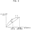
- the LED current controlled by the driver 1 may be shaped with approximately square waves as illustrated in FIG. 2 . If the peak value of the square wave is approximate to the maximum rated current of the LED 6 and its minimum value is approximately 0, the LED current and the average luminance of the LED 6 by the LED current is as illustrated in FIG. 3 , by averaging the square waves.
- an X axis indicates LED current and a Y axis indicates LED light output.
- the average luminance of the LED provided by the LED current, shaped with square waves, is represented in the form of a straight line B, connecting a starting point of X-Y coordinates to the luminance value of the LED corresponding to the maximum rated current of the LED.
- constant current direct current that is approximately constant in magnitude
- luminance of the LED 6 by the LED current is the same as a curve A depicted in FIG. 3 .
- a relationship between current and luminance is not linear, but shows an exponential function wherein the light output of the LED 6 is saturated if the LED current is larger than a predetermined magnitude.
- a difference D 1 occurs between the luminance (A) and the average luminance (B) of the LED 6 respectively to the constant current and the square wave current, as depicted in FIG. 3 .
- the difference in efficiency between the luminance (A) and the average luminance (B) of the LED 6 respectively to the constant current and the square wave current is about 15% in terms of power.
- controlling the LED current which is a periodical direct current is less efficient than controlling the LED current which is the constant current, in terms of power consumption.
- aspects of the present invention are achieved by providing a light emitting diode (LED) driver to drive an LED, comprising a current adjusting unit to adjust magnitude of a current flowing on the LED by supplying power from a power supply device to the LED and cutting off the power; a modulation control unit to modulate a waveform of the current flowing on the LED by controlling the adjustment operation of the current adjusting unit; and a constant current offset unit to control the adjustment operation of the current adjusting unit so that the current flowing on the LED is higher or equal to a predetermined value as the waveform thereof is modulated.
- LED light emitting diode
- the current adjusting unit comprises a switching unit to input an ON or OFF signal to thereby supply power to the LED from a power supply device and cut off the power; a regulating unit to regulate the current flowing on the LED so that it is not abruptly changed; a current detecting unit to detect the current flowing on the LED; and a switching control unit to output a signal to turn off the switching unit when the current detected by the current detecting unit is determined to be higher than or equal to a first threshold, but to output a signal to turn on the switching unit when the current detected by the current detecting unit is determined to be less than the first threshold.
- the modulation control unit inputs a predetermined pulse width modulation (PWM) signal to thereby supply an output signal of the switching control unit to the switching unit and to cut off the output signal.
- PWM pulse width modulation
- the constant current offset unit outputs a signal to turn off the switching unit when the current flowing on the LED detected by the current detecting unit is determined to be higher than or equal to a second threshold and the output signal from the switching control unit is cut off, but outputs a signal to turn on the switching unit when the current flowing on the LED is determined to be less than the second threshold.
- the constant current offset unit comprises a comparator to compare a voltage corresponding to the current flowing on the LED, which is detected by the current detecting unit, with a voltage corresponding to the second threshold, and output a logic HIGH signal when the voltage corresponding to the current flowing on the LED is higher; a set-reset (S-R) flip flop to set an output signal from the comparator as a RESET input and a pulse signal having a predetermined frequency as a SET input; and an OR gate to receive an output signal from the S-R flip flop and an output signal from the modulation control unit, outputting the logical sum of the received output signals to the switching unit.
- S-R set-reset
- FIG. 1 is a circuit diagram illustrating a circuit configuration of a conventional LED driver
- FIG. 2 is a waveform diagram schematically illustrating a waveform of a current flowing on an LED driven by the LED driver of FIG. 1 ;
- FIG. 3 illustrates a comparison of an LED current with a predetermined constant current in terms of an LED light output
- FIG. 4 is a block diagram schematically illustrating a configuration of an LED driver according to an exemplary embodiment of the present invention
- FIG. 5 is a circuit diagram illustrating an exemplary circuit configuration of the LED driver of FIG. 4 ;
- FIG. 6 is a waveform diagram schematically illustrating a waveform of a current flowing on an LED driven by the LED driver of FIG. 5 ;
- FIG. 7 illustrates a comparison of an LED current with a predetermined constant current in terms of an LED light output of FIG. 6 .
- FIG. 4 is a block diagram illustrating an internal configuration of an LED driver 10 according to an exemplary embodiment of the present invention.
- the LED driver 10 drives an LED 60 which may be used as a backlight for a liquid crystal display and so on.
- the LED driver 10 adjusts the luminance of the light emitted by the LED 60 , by controlling current flowing on the LED 60 supplied with power from a source.
- the LED driver 10 controls the luminance of the LED 60 , by adjusting a peak value of an LED current and modulating a waveform of the LED current, and also supplies an offset current so as to allow the LED current to maintain at least a predetermined constant level.
- the LED driver 10 as illustrated in FIG. 4 , comprises a current adjusting unit 20 , a modulation control unit 40 and a constant current offset unit 50 .
- the current adjusting unit 20 adjusts a magnitude of the current flowing on the LED 60 through so-called analog dimming.
- a circuit configuration of the current adjusting unit 20 according to this exemplary embodiment is illustrated in FIG. 5 .
- the current adjusting unit 20 comprises a switching unit 22 , a regulating unit 24 , a current detecting unit 26 and a switching control unit 28 .
- the switching unit 22 inputs an ON or OFF signal, thereby supplying or not supplying the LED 60 with power from a power supply unit 70 , according to either the ON or OFF signal inputted.
- the switching unit 22 is embodied with a metal oxide semiconductor field-effect transistor (MOSFET). Into a gate of the MOSFET of the switching unit 22 is inputted an output signal from the switching control unit 28 .
- MOSFET metal oxide semiconductor field-effect transistor
- the regulating unit 24 regulates the current flowing on the LED 60 so as not to be abruptly changed.
- the regulating unit 24 is embodied with a diode 242 and an inductor 244 .
- the diode 242 and the inductor 244 are connected to the power supply unit 70 in parallel, and the inductor 244 is connected to the LED 60 in series.
- An anode of the diode 242 is connected to a drain of the MOSFET in the switching unit 22 , and a cathode thereof is connected to the power supply unit 70 .
- the switching unit 22 inputs an ON signal whereby the drain and a source of the MOSFET in the switching unit 22 are electrically connected, and the current flows on the LED 60 by a voltage Vin of the power supply unit 70 through the inductor 244 .
- the inductor is charged with current energy, and the LED current increases by a predetermined value.
- the switching unit 22 If electrical connection between the drain and the source of the MOSFET in the switching unit 22 is broken the switching unit 22 inputs an OFF signal.
- the inductor 244 , the LED 60 and the diode 242 constitutes a closed circuit. Accordingly, the current flows on the LED 60 by the energy stored in the inductor 244 . In this case, the LED current is reduced as the current energy of the inductor 244 is discharged.
- the current detecting unit 26 detects the current flowing on the LED 60 .
- the current detecting unit 26 is embodied with a resistor having a resistance value of R. At this time, since the current flowing on the resister is of the same as the current flowing on the LED 60 , the LED current is estimated by use of the voltage applied to an input terminal of the resister.
- the switching control unit 28 When the current detecting unit 26 determines that the current detected thereby is larger than or equal to a predetermined first threshold, the switching control unit 28 turns off the switching unit 22 . When the current detected by the current detecting unit 26 is determined to be less than the first threshold, the switching control unit 28 turns on the switching unit 22 .
- the switching control unit 28 evaluates the magnitude of the current flowing on the LED 60 , and adjusts the magnitude of the LED current, by comparing it with the first threshold capable of being preset or adjusted and outputting a signal to turn on or off the switching unit 22 so that the LED current can maintain the current value around the first threshold.
- the switching control unit 28 in this exemplary embodiment comprises two comparators 282 and 284 , an OR gate 288 , an oscillator 290 and an S-R flip flop 292 .
- the two comparators 282 and 284 may be embodied with operational amplifiers (OP-amp), and a voltage across the resistor of the current detecting unit 26 is applied to each non-inverting input terminal thereof.
- OP-amp operational amplifiers
- a reference voltage Vr is applied to an inverting input terminal of the comparator 284 .
- the comparator 284 When the voltage across the resistor of the current detecting unit 26 , i.e., the voltage corresponding to the LED current, is higher than the reference voltage Vr, the comparator 284 outputs a logic HIGH signal. It is preferred that the reference voltage Vr is determined with the consideration of the maximum rated current and the resistance value R of the LED 60 .
- a predetermined voltage from outside is applied to the inverting input terminal of the comparator 282 .
- the comparator 284 When the voltage across the resistor of the current detecting unit 26 , that is, the voltage corresponding to the LED current is higher than a predetermined input voltage, the comparator 284 outputs a logic HIGH signal. In this case, the voltage externally applied is less than the voltage corresponding to the maximum rated current, but it corresponds to the current determined not to exceed the LED current.
- the logical sum of output signals from the two comparators 282 and 284 is applied to a RESET input of the S-R flip flop 292 through an OR gate.
- An output signal of the oscillator 290 is applied to a SET input of the S-R flip flop 292 .
- the oscillator 290 outputs a pulse signal of a predetermined frequency.
- the S-R flip flop 292 outputs a corresponding logic HIGH signal, and maintains it.
- the S-R flip flop 292 outputs a logic LOW signal. That is, the S-R flip flop 292 outputs a logic LOW signal when the voltage corresponding to the LED current is higher than the reference voltage Vr or the voltage externally adjusted, but it outputs logic HIGH signals in the other cases. Therefore, the switching control unit 28 adjusts the magnitude of the LED current by outputting a signal to turn on or off, so that the LED current can maintain a predetermined peak value within the limitation that it does not exceed the maximum rated current.
- the modulation control unit 40 modulates a waveform of the LED current by controlling an operation of the current adjusting unit 20 , thereby adjusting the luminance of the light outputted by the LED current.
- the modulation control unit 40 inputs a pulse width modulation (PWM) signal, and supplies or does not supply an output signal of the switching control unit 28 to the switching unit 22 according to the signal inputted.
- PWM pulse width modulation
- the modulation control unit 40 of this exemplary embodiment is embodied with a buffer 44 and an AND gate 42 .
- the AND gate 42 has two input terminals: a PWM signal is applied to one input terminal through the buffer 44 from the outside, and an output signal of the switching control unit 28 is applied to the other input terminal.
- the AND gate 42 outputs a signal for logical multiplication of the two input signals.
- the PWM signal inputted by the AND gate 42 is a pulse signal having predetermined period and duration.
- the output signal of the switching control unit 28 becomes identical to the output signal of the AND gate 42 .
- the output signal of the AND gate 42 becomes logically LOW. Accordingly, the output signal of the switching control unit 28 is not transmitted to the switching unit 22 although it is logically HIGH, whereby the switching unit 22 is not turned on.
- the magnitude of the average current flowing on the LED 60 may be adjusted by properly adjusting the pulse width or the duty cycle of the PWM signal.
- the average current flowing on the LED 60 increases if the pulse width or duty cycle of the PWM signal increases, whereas the average current flowing on the LED 60 decreases if the pulse width or duty cycle of the PWM signal is reduced.
- the peak current is more promptly adjusted in comparison with the pulse width control, by setting up a period of the PWM signal sufficiently longer than that of the oscillator 290 .
- the constant current offset unit 50 provides control so that the current flowing on the LED 60 maintains its predetermined size. That is, the constant current offset unit 50 provides control so that a predetermined size of constant current additionally flows on the LED 60 on which the current shaped with approximately square waves becomes flowing by the pulse width control.
- the constant current offset unit 50 of this exemplary embodiment outputs a signal to turn off the switching unit 22 when the current detecting unit 26 determines the LED current detected thereby to be higher than or equal to the predetermined second threshold, and the output signal of the switching control unit 28 to be broken. But the constant current offset unit 50 outputs a signal to turn on the switching unit 22 when the LED current is determined to be less than the second threshold value.
- the constant current offset unit 50 when the current flowing on the LED 60 is less than the reference value established externally, the constant current offset unit 50 outputs a signal to turn on the switching unit 22 , thereby allowing the current having at least the reference value to flow on the LED 60 .
- the constant current offset unit 50 of this exemplary embodiment comprises a comparator 52 , an S-R flip flop 54 and an OR gate 56 .
- the comparator 52 can be embodied with an OP-amp by way of example.
- To an inverting input terminal of the comparator 52 is applied a voltage corresponding to the magnitude of current to be offset as a voltage that can be set up externally, and a voltage across both terminals of the current detecting unit 26 is applied to a non-inverting input terminal thereof.
- the comparator 52 outputs a logical HIGH signal when the voltages across both terminals of the current detecting unit 26 , that is, the voltage corresponding to the LED current, is higher than the voltage corresponding to the current value externally established.
- An output signal from the oscillator 290 is applied to a SET input terminal of the S-R flip flop 54 , and an output signal from the comparator 52 is applied to a RESET input terminal thereof.
- the operation of the S-R flip flop 54 is similar to that of the S-R flip flop 292 .
- the S-R flip flop 54 outputs a logical LOW signal, but it outputs a logical HIGH signal in the other cases.
- the OR gate 56 receives output signals from the modulation control unit 40 and the S-R flip flop 54 respectively, thereby outputting a logical OR signal thereof to a gate input terminal of the switching unit 22 . That is, the OR gate 56 outputs a logical HIGH signal to turn on the switching unit 22 when the LED current is less than the externally established current value, while it outputs a logical LOW signal to turn off the switching unit 22 when the LED current is higher than the externally established current value and the PWM signal is logically LOW.
- FIG. 6 A waveform of the current flowing on the LED 60 by the LED driver 10 according to this exemplary embodiment as described above is illustrated in FIG. 6 .
- the LED current demonstrates a waveform created by combining the square wave with an offset current of a predetermined constant level.
- the luminance of the light output of the LED 60 due to the current flowing on the LED 60 by the LED driver 10 according to this exemplary embodiment is illustrated in FIG. 7 .
- the luminance of the light output of the LED 60 is indicated in the form of a straight line C when the magnitude of the offset current is 30% of the maximum rated current.
- a difference (D 2 ) from the luminance A due to the constant current identical in magnitude to the average current thereof becomes approximately 5% in view of the power efficiency.
- the power efficiency may be enhanced by about 10%, but the loss of power may be 15% when there is no offset current.
- the present invention can provide an LED driver having improved efficiency in power consumption.
- the modulation control unit can be variously worked so that the LED current becomes a periodical direct current shaped with a sine wave, a triangular wave as well as a square wave.
Abstract
Description
Claims (5)
Applications Claiming Priority (2)
| Application Number | Priority Date | Filing Date | Title |
|---|---|---|---|
| KR2005-0009654 | 2005-02-02 | ||
| KR1020050009654A KR100628716B1 (en) | 2005-02-02 | 2005-02-02 | Led driver |
Publications (2)
| Publication Number | Publication Date |
|---|---|
| US20060170373A1 US20060170373A1 (en) | 2006-08-03 |
| US7295176B2 true US7295176B2 (en) | 2007-11-13 |
Family
ID=36228806
Family Applications (1)
| Application Number | Title | Priority Date | Filing Date |
|---|---|---|---|
| US11/342,572 Expired - Fee Related US7295176B2 (en) | 2005-02-02 | 2006-01-31 | LED driver with constant current offset unit |
Country Status (4)
| Country | Link |
|---|---|
| US (1) | US7295176B2 (en) |
| EP (1) | EP1689213A1 (en) |
| KR (1) | KR100628716B1 (en) |
| CN (1) | CN100583213C (en) |
Cited By (20)
| Publication number | Priority date | Publication date | Assignee | Title |
|---|---|---|---|---|
| US20080037303A1 (en) * | 2006-08-10 | 2008-02-14 | Kazuharu Mishimagi | Light Emitting Device |
| US20080067953A1 (en) * | 2006-09-14 | 2008-03-20 | Infineon Technologies | Controlling power to light-emitting device |
| US20080278138A1 (en) * | 2007-05-08 | 2008-11-13 | Qi Cui Wei | High accuracy constant-off average output current control scheme |
| US20100045190A1 (en) * | 2008-08-20 | 2010-02-25 | White Electronic Designs Corporation | Led backlight |
| CN101673509A (en) * | 2008-09-09 | 2010-03-17 | 富士胶片株式会社 | Display apparatus |
| US20100117555A1 (en) * | 2008-11-12 | 2010-05-13 | Monolithic Power Systems, Inc. | Pulse dimming circuit and the method thereof |
| US20100259180A1 (en) * | 2009-04-10 | 2010-10-14 | Yuancheng Ren | Led circuit and method for controlling the average current of the led |
| US7898187B1 (en) * | 2007-02-08 | 2011-03-01 | National Semiconductor Corporation | Circuit and method for average-current regulation of light emitting diodes |
| US20120262082A1 (en) * | 2011-04-18 | 2012-10-18 | Esaki Sana | Semiconductor light-emiting element driver circuit and light fixture using the same |
| US20130141017A1 (en) * | 2011-12-05 | 2013-06-06 | Panasonic Corporation | Lighting apparatus and illuminating fixture with the same |
| US20130141002A1 (en) * | 2011-12-05 | 2013-06-06 | Panasonic Corporation | Lighting apparatus and illuminating fixture with the same |
| US8476847B2 (en) | 2011-04-22 | 2013-07-02 | Crs Electronics | Thermal foldback system |
| US8502454B2 (en) | 2008-02-08 | 2013-08-06 | Innosys, Inc | Solid state semiconductor LED replacement for fluorescent lamps |
| US8502477B2 (en) | 2009-04-11 | 2013-08-06 | Innosys, Inc | Dimmable power supply |
| US8669711B2 (en) | 2011-04-22 | 2014-03-11 | Crs Electronics | Dynamic-headroom LED power supply |
| US8669715B2 (en) | 2011-04-22 | 2014-03-11 | Crs Electronics | LED driver having constant input current |
| US8773031B2 (en) | 2010-11-22 | 2014-07-08 | Innosys, Inc. | Dimmable timer-based LED power supply |
| US8987997B2 (en) | 2012-02-17 | 2015-03-24 | Innosys, Inc. | Dimming driver with stealer switch |
| US9559675B1 (en) * | 2014-02-24 | 2017-01-31 | Marvell International Ltd. | Current shaping scheme in TRIAC dimmable LED driver |
| US10827585B1 (en) | 2019-04-17 | 2020-11-03 | Goodrich Lighting Systems, Inc. | Driving light emitting diodes and display apparatus |
Families Citing this family (39)
| Publication number | Priority date | Publication date | Assignee | Title |
|---|---|---|---|---|
| US7259525B2 (en) * | 2005-11-03 | 2007-08-21 | System General Corporation | High efficiency switching LED driver |
| KR100738463B1 (en) * | 2006-08-22 | 2007-07-11 | 주식회사 우영 | Apparatus of driving light emitting diode |
| KR101215513B1 (en) * | 2006-10-17 | 2013-01-09 | 삼성디스플레이 주식회사 | Gate on voltage/led driving voltage generator and dc/dc converter including the same and liquid crystal display having the same and aging test apparatus for liquid crystal display |
| KR101176533B1 (en) * | 2007-01-25 | 2012-08-24 | 삼성전자주식회사 | PWM dimming control method and display apparatus having PWM dimming control function |
| KR100893193B1 (en) * | 2007-06-26 | 2009-04-16 | 주식회사 우영 | Apparatus for power supply and light emitting diode light therewith |
| KR100887087B1 (en) * | 2007-06-26 | 2009-03-04 | 삼성전기주식회사 | Led driving apparatus of theater dimming buck type |
| CN101389177A (en) * | 2007-09-14 | 2009-03-18 | 群康科技(深圳)有限公司 | Light regulating circuit |
| NL1034616C2 (en) * | 2007-11-01 | 2009-05-06 | E L Boer Holding | LED lamp dimmer i.e. wall mount LED lamp dimmer, for use in e.g. home, has control unit with controller for regulating pressure or pulse width modulation, so that flow of current passing through regular flow system is limited |
| WO2009060368A2 (en) | 2007-11-05 | 2009-05-14 | Philips Intellectual Property & Standards Gmbh | Device for driving a load |
| FR2931616B1 (en) * | 2008-05-26 | 2010-08-20 | Ece | DEVICE FOR SUPPLYING A SET OF LIGHTING DEVICES. |
| US8093826B1 (en) * | 2008-08-26 | 2012-01-10 | National Semiconductor Corporation | Current mode switcher having novel switch mode control topology and related method |
| TWI390490B (en) * | 2008-12-03 | 2013-03-21 | Au Optronics Corp | Light emitting diode backlight module and driving apparatus and method thereof |
| US8013544B2 (en) * | 2008-12-10 | 2011-09-06 | Linear Technology Corporation | Dimmer control leakage pull down using main power device in flyback converter |
| US8089216B2 (en) * | 2008-12-10 | 2012-01-03 | Linear Technology Corporation | Linearity in LED dimmer control |
| US8692481B2 (en) * | 2008-12-10 | 2014-04-08 | Linear Technology Corporation | Dimmer-controlled LEDs using flyback converter with high power factor |
| US8310172B2 (en) * | 2008-12-10 | 2012-11-13 | Linear Technology Corporation | Current ripple reduction circuit for LEDs |
| TWI407837B (en) * | 2008-12-18 | 2013-09-01 | Novatek Microelectronics Corp | Led illuninant driving circuit and automatic brightness compensation method thereof |
| CN101436393B (en) * | 2008-12-24 | 2012-04-18 | 友达光电股份有限公司 | LED backlight module and drive circuit and method thereof |
| CN101916541B (en) * | 2009-05-08 | 2014-07-30 | 北京中庆微数字设备开发有限公司 | Row scanning stop protection circuit |
| US8405319B2 (en) * | 2009-05-09 | 2013-03-26 | Laurence P. Sadwick | Universal dimmer |
| WO2010131158A2 (en) * | 2009-05-12 | 2010-11-18 | Koninklijke Philips Electronics, N.V. | Intelligent dimmer for managing a lighting load |
| US8536803B2 (en) * | 2009-07-16 | 2013-09-17 | Innosys, Inc | Fluorescent lamp power supply |
| DE102010031845A1 (en) * | 2010-07-22 | 2012-01-26 | Hella Kgaa Hueck & Co. | Circuit device for controlling power supply to LED, has pulse width modulation signal input terminal that is connected with input terminal of switching circuit for switching ON/OFF state of static converter |
| AU2011281033A1 (en) | 2010-07-22 | 2013-02-07 | Independence Led Lighting, Llc | Light engine device with direct to linear system driver |
| AT12464U1 (en) * | 2010-10-08 | 2012-05-15 | Tridonic Ag | OPERATING CIRCUIT FOR LIGHT DIODES |
| JP5576818B2 (en) * | 2011-03-22 | 2014-08-20 | パナソニック株式会社 | Lighting device and lighting fixture using the same |
| US8723425B2 (en) | 2011-06-17 | 2014-05-13 | Stevan Pokrajac | Light emitting diode driver circuit |
| US20130057462A1 (en) * | 2011-09-06 | 2013-03-07 | Xiang Yang | LED Driving Circuit, Liquid Crystal Display Device and Driving Method Thereof |
| CN102306485A (en) * | 2011-09-06 | 2012-01-04 | 深圳市华星光电技术有限公司 | Light emitting diode (LED) driving circuit, liquid crystal display device and LED driving method |
| US9660535B2 (en) * | 2011-11-11 | 2017-05-23 | Microchip Technology Incorporated | Method and system to dynamically position a switch mode power supply output voltage |
| US9882497B2 (en) | 2012-09-28 | 2018-01-30 | Microchip Technology Incorporated | Soft switching synchronous quasi resonant converter |
| AT13857U1 (en) * | 2013-04-30 | 2014-10-15 | Tridonic Gmbh & Co Kg | Error detection for LEDs |
| AT14074U1 (en) * | 2013-04-30 | 2015-04-15 | Tridonic Gmbh & Co Kg | Operating circuit for LED |
| JP2015076923A (en) * | 2013-10-07 | 2015-04-20 | ローム株式会社 | Switching converter, control circuit and control method for the same, and lighting device and electronic apparatus using the same |
| JP6252231B2 (en) * | 2014-02-21 | 2017-12-27 | サンケン電気株式会社 | LED lighting device |
| US10201052B1 (en) * | 2017-09-22 | 2019-02-05 | Linear Technology Holding, LLC | LED dimming |
| CN112930005B (en) * | 2021-02-01 | 2023-05-26 | 苏州华兴源创科技股份有限公司 | Light source driving method and circuit |
| CN114038415B (en) * | 2021-12-13 | 2022-08-23 | Tcl华星光电技术有限公司 | Pixel circuit and display panel |
| CN114302531B (en) * | 2022-01-05 | 2022-10-18 | 北京芯格诺微电子有限公司 | LED dimming control method and dimming driving device |
Citations (12)
| Publication number | Priority date | Publication date | Assignee | Title |
|---|---|---|---|---|
| JPH10284282A (en) | 1997-04-04 | 1998-10-23 | Sharp Corp | Inverter circuit for driving liquid crystal back light |
| JP2001308384A (en) | 2000-04-20 | 2001-11-02 | Fujitsu General Ltd | Light-emitting element drive control system |
| US6320330B1 (en) * | 1999-01-22 | 2001-11-20 | Nokia Mobile Phones Ltd | Illuminating electronic device and illumination method |
| US6329764B1 (en) | 2000-04-19 | 2001-12-11 | Van De Ven Antony | Method and apparatus to improve the color rendering of a solid state light source |
| EP1229764A2 (en) | 2001-02-05 | 2002-08-07 | Pioneer Corporation | Light emitting diode driving circuit |
| KR20030050990A (en) | 2001-12-20 | 2003-06-25 | 삼성전기주식회사 | Inverter for back-light of LCD |
| KR20040019544A (en) | 2002-08-28 | 2004-03-06 | 삼성전자주식회사 | Apparatus for controlling lcd backlight in mobile station |
| US20040135522A1 (en) | 2003-01-15 | 2004-07-15 | Luminator Holding, L.P. | Led lighting system |
| US20040208011A1 (en) | 2002-05-07 | 2004-10-21 | Sachito Horiuchi | Light emitting element drive device and electronic device having light emitting element |
| WO2004100614A1 (en) | 2003-05-07 | 2004-11-18 | Koninklijke Philips Electronics N.V. | Current control method and circuit for light emitting diodes |
| US6909249B2 (en) * | 2002-12-12 | 2005-06-21 | Toko Kabushiki Kaisha | Switching constant-current power supply |
| US7071762B2 (en) * | 2001-01-31 | 2006-07-04 | Koninklijke Philips Electronics N.V. | Supply assembly for a led lighting module |
Family Cites Families (3)
| Publication number | Priority date | Publication date | Assignee | Title |
|---|---|---|---|---|
| JPH10171406A (en) | 1996-12-10 | 1998-06-26 | Toshiba Lighting & Technol Corp | Information display device |
| JPH10171407A (en) | 1996-12-10 | 1998-06-26 | Toshiba Lighting & Technol Corp | Information displaying device |
| JP2000347613A (en) | 1999-06-03 | 2000-12-15 | Mitsubishi Electric Corp | Driving circuit for light emitting diode |
-
2005
- 2005-02-02 KR KR1020050009654A patent/KR100628716B1/en active IP Right Grant
-
2006
- 2006-01-17 CN CN200610005078A patent/CN100583213C/en not_active Expired - Fee Related
- 2006-01-27 EP EP06100993A patent/EP1689213A1/en not_active Withdrawn
- 2006-01-31 US US11/342,572 patent/US7295176B2/en not_active Expired - Fee Related
Patent Citations (12)
| Publication number | Priority date | Publication date | Assignee | Title |
|---|---|---|---|---|
| JPH10284282A (en) | 1997-04-04 | 1998-10-23 | Sharp Corp | Inverter circuit for driving liquid crystal back light |
| US6320330B1 (en) * | 1999-01-22 | 2001-11-20 | Nokia Mobile Phones Ltd | Illuminating electronic device and illumination method |
| US6329764B1 (en) | 2000-04-19 | 2001-12-11 | Van De Ven Antony | Method and apparatus to improve the color rendering of a solid state light source |
| JP2001308384A (en) | 2000-04-20 | 2001-11-02 | Fujitsu General Ltd | Light-emitting element drive control system |
| US7071762B2 (en) * | 2001-01-31 | 2006-07-04 | Koninklijke Philips Electronics N.V. | Supply assembly for a led lighting module |
| EP1229764A2 (en) | 2001-02-05 | 2002-08-07 | Pioneer Corporation | Light emitting diode driving circuit |
| KR20030050990A (en) | 2001-12-20 | 2003-06-25 | 삼성전기주식회사 | Inverter for back-light of LCD |
| US20040208011A1 (en) | 2002-05-07 | 2004-10-21 | Sachito Horiuchi | Light emitting element drive device and electronic device having light emitting element |
| KR20040019544A (en) | 2002-08-28 | 2004-03-06 | 삼성전자주식회사 | Apparatus for controlling lcd backlight in mobile station |
| US6909249B2 (en) * | 2002-12-12 | 2005-06-21 | Toko Kabushiki Kaisha | Switching constant-current power supply |
| US20040135522A1 (en) | 2003-01-15 | 2004-07-15 | Luminator Holding, L.P. | Led lighting system |
| WO2004100614A1 (en) | 2003-05-07 | 2004-11-18 | Koninklijke Philips Electronics N.V. | Current control method and circuit for light emitting diodes |
Cited By (27)
| Publication number | Priority date | Publication date | Assignee | Title |
|---|---|---|---|---|
| US7777421B2 (en) * | 2006-08-10 | 2010-08-17 | Kazuharu Mishimagi | Light emitting device |
| US20080037303A1 (en) * | 2006-08-10 | 2008-02-14 | Kazuharu Mishimagi | Light Emitting Device |
| US20080067953A1 (en) * | 2006-09-14 | 2008-03-20 | Infineon Technologies | Controlling power to light-emitting device |
| US7557519B2 (en) * | 2006-09-14 | 2009-07-07 | Infineon Technologies Ag | Controlling power to light-emitting device |
| US7898187B1 (en) * | 2007-02-08 | 2011-03-01 | National Semiconductor Corporation | Circuit and method for average-current regulation of light emitting diodes |
| US20080278138A1 (en) * | 2007-05-08 | 2008-11-13 | Qi Cui Wei | High accuracy constant-off average output current control scheme |
| US8502454B2 (en) | 2008-02-08 | 2013-08-06 | Innosys, Inc | Solid state semiconductor LED replacement for fluorescent lamps |
| US20100045190A1 (en) * | 2008-08-20 | 2010-02-25 | White Electronic Designs Corporation | Led backlight |
| CN101673509A (en) * | 2008-09-09 | 2010-03-17 | 富士胶片株式会社 | Display apparatus |
| US20100117555A1 (en) * | 2008-11-12 | 2010-05-13 | Monolithic Power Systems, Inc. | Pulse dimming circuit and the method thereof |
| US8098018B2 (en) * | 2008-11-12 | 2012-01-17 | Monolithic Power Systems, Inc. | Pulse dimming circuit and the method thereof |
| US20100259180A1 (en) * | 2009-04-10 | 2010-10-14 | Yuancheng Ren | Led circuit and method for controlling the average current of the led |
| US8247984B2 (en) * | 2009-04-10 | 2012-08-21 | Monolithic Power Systems, Inc. | LED circuit and method for controlling the average current of the LED |
| US8502477B2 (en) | 2009-04-11 | 2013-08-06 | Innosys, Inc | Dimmable power supply |
| US8773031B2 (en) | 2010-11-22 | 2014-07-08 | Innosys, Inc. | Dimmable timer-based LED power supply |
| US20120262082A1 (en) * | 2011-04-18 | 2012-10-18 | Esaki Sana | Semiconductor light-emiting element driver circuit and light fixture using the same |
| US8680788B2 (en) * | 2011-04-18 | 2014-03-25 | Panasonic Corporation | Semiconductor light-emiting element driver circuit and light fixture using the same |
| US8476847B2 (en) | 2011-04-22 | 2013-07-02 | Crs Electronics | Thermal foldback system |
| US8669711B2 (en) | 2011-04-22 | 2014-03-11 | Crs Electronics | Dynamic-headroom LED power supply |
| US8669715B2 (en) | 2011-04-22 | 2014-03-11 | Crs Electronics | LED driver having constant input current |
| US20130141002A1 (en) * | 2011-12-05 | 2013-06-06 | Panasonic Corporation | Lighting apparatus and illuminating fixture with the same |
| US20130141017A1 (en) * | 2011-12-05 | 2013-06-06 | Panasonic Corporation | Lighting apparatus and illuminating fixture with the same |
| US9295115B2 (en) * | 2011-12-05 | 2016-03-22 | Panasonic Intellectual Property Management Co., Ltd. | Lighting apparatus and illuminating fixture with the same |
| US9585209B2 (en) * | 2011-12-05 | 2017-02-28 | Panasonic Intellectual Property Management Co., Ltd. | Lighting apparatus and illuminating fixture with the same |
| US8987997B2 (en) | 2012-02-17 | 2015-03-24 | Innosys, Inc. | Dimming driver with stealer switch |
| US9559675B1 (en) * | 2014-02-24 | 2017-01-31 | Marvell International Ltd. | Current shaping scheme in TRIAC dimmable LED driver |
| US10827585B1 (en) | 2019-04-17 | 2020-11-03 | Goodrich Lighting Systems, Inc. | Driving light emitting diodes and display apparatus |
Also Published As
| Publication number | Publication date |
|---|---|
| KR100628716B1 (en) | 2006-09-28 |
| US20060170373A1 (en) | 2006-08-03 |
| CN100583213C (en) | 2010-01-20 |
| KR20060088713A (en) | 2006-08-07 |
| CN1815542A (en) | 2006-08-09 |
| EP1689213A1 (en) | 2006-08-09 |
Similar Documents
| Publication | Publication Date | Title |
|---|---|---|
| US7295176B2 (en) | LED driver with constant current offset unit | |
| KR100771780B1 (en) | Led driving apparatus having fuction of over-voltage protection and duty control | |
| US8541956B2 (en) | Light emitting diode driving method and driving circuit | |
| US7358685B2 (en) | DC-DC converter having protective function of over-voltage and over-current and led driving circuit using the same | |
| US7564434B2 (en) | Light emitting diode driving circuit for backlight having constant current control function | |
| US8339053B2 (en) | LED dimming apparatus | |
| US8289305B2 (en) | Backlight unit, liquid crystal display device having the same and control method thereof | |
| US9271369B2 (en) | LED driver apparatus | |
| WO2016095309A1 (en) | Liquid crystal display device, backlight module, and backlight source driving circuit thereof | |
| US20040124889A1 (en) | Led drive circuit | |
| US9603220B2 (en) | LED driver apparatus | |
| US8217584B2 (en) | Driving circuit for driving light emitting diodes and dimmer | |
| JP2008288207A (en) | Led array driving device | |
| US9295119B2 (en) | Lighting device and illumination apparatus using the same | |
| US20110140626A1 (en) | Electronic driver dimming control using ramped pulsed modulation for large area solid-state oleds | |
| TW201406207A (en) | Controller and method for dimming and electronic system thereof | |
| KR20120095245A (en) | Pwm controlling circuit and led driver circuit having the same in | |
| US7755297B2 (en) | Display apparatus and control method thereof | |
| JP2007215318A (en) | Switching regulator | |
| US7965048B2 (en) | Switching converter for lighting with light intensity as feedback and light emitting apparatus using the same | |
| US20160119988A1 (en) | Dual control led driver | |
| KR100725499B1 (en) | Led driving circuit | |
| JP2008283206A (en) | Led lighting device | |
| KR20130044747A (en) | Over voltage protection circuit in led | |
| JP2012074693A (en) | Driver circuit for light-emitting component |
Legal Events
| Date | Code | Title | Description |
|---|---|---|---|
| AS | Assignment |
Owner name: SAMSUNG ELECTRONICS CO., LTD., KOREA, REPUBLIC OF Free format text: ASSIGNMENT OF ASSIGNORS INTEREST;ASSIGNOR:YANG, JOON-HYUN;REEL/FRAME:017523/0844 Effective date: 20060119 |
|
| STCF | Information on status: patent grant |
Free format text: PATENTED CASE |
|
| FEPP | Fee payment procedure |
Free format text: PAYOR NUMBER ASSIGNED (ORIGINAL EVENT CODE: ASPN); ENTITY STATUS OF PATENT OWNER: LARGE ENTITY |
|
| FEPP | Fee payment procedure |
Free format text: PAYER NUMBER DE-ASSIGNED (ORIGINAL EVENT CODE: RMPN); ENTITY STATUS OF PATENT OWNER: LARGE ENTITY |
|
| FEPP | Fee payment procedure |
Free format text: PAYOR NUMBER ASSIGNED (ORIGINAL EVENT CODE: ASPN); ENTITY STATUS OF PATENT OWNER: LARGE ENTITY |
|
| FPAY | Fee payment |
Year of fee payment: 4 |
|
| FPAY | Fee payment |
Year of fee payment: 8 |
|
| FEPP | Fee payment procedure |
Free format text: MAINTENANCE FEE REMINDER MAILED (ORIGINAL EVENT CODE: REM.); ENTITY STATUS OF PATENT OWNER: LARGE ENTITY |
|
| LAPS | Lapse for failure to pay maintenance fees |
Free format text: PATENT EXPIRED FOR FAILURE TO PAY MAINTENANCE FEES (ORIGINAL EVENT CODE: EXP.); ENTITY STATUS OF PATENT OWNER: LARGE ENTITY |
|
| STCH | Information on status: patent discontinuation |
Free format text: PATENT EXPIRED DUE TO NONPAYMENT OF MAINTENANCE FEES UNDER 37 CFR 1.362 |
|
| FP | Lapsed due to failure to pay maintenance fee |
Effective date: 20191113 |