US7251797B2 - Pessimism reduction in crosstalk noise aware static timing analysis - Google Patents
Pessimism reduction in crosstalk noise aware static timing analysis Download PDFInfo
- Publication number
- US7251797B2 US7251797B2 US10/994,858 US99485804A US7251797B2 US 7251797 B2 US7251797 B2 US 7251797B2 US 99485804 A US99485804 A US 99485804A US 7251797 B2 US7251797 B2 US 7251797B2
- Authority
- US
- United States
- Prior art keywords
- victim
- timing
- window
- switching time
- delay
- Prior art date
- Legal status (The legal status is an assumption and is not a legal conclusion. Google has not performed a legal analysis and makes no representation as to the accuracy of the status listed.)
- Expired - Fee Related, expires
Links
- 238000004458 analytical method Methods 0.000 title claims abstract description 94
- 230000003068 static effect Effects 0.000 title claims abstract description 31
- 230000009467 reduction Effects 0.000 title description 4
- 238000000034 method Methods 0.000 claims abstract description 83
- 230000009471 action Effects 0.000 claims abstract description 21
- 230000008569 process Effects 0.000 claims abstract description 15
- 238000004364 calculation method Methods 0.000 claims description 8
- 239000004065 semiconductor Substances 0.000 claims description 8
- 230000003190 augmentative effect Effects 0.000 claims description 2
- 238000013459 approach Methods 0.000 description 18
- 238000013461 design Methods 0.000 description 17
- 230000001934 delay Effects 0.000 description 11
- 239000003990 capacitor Substances 0.000 description 9
- 230000007423 decrease Effects 0.000 description 5
- 238000010586 diagram Methods 0.000 description 5
- 230000006870 function Effects 0.000 description 5
- 230000003071 parasitic effect Effects 0.000 description 5
- 230000007704 transition Effects 0.000 description 5
- 230000008859 change Effects 0.000 description 4
- 230000008878 coupling Effects 0.000 description 4
- 238000010168 coupling process Methods 0.000 description 4
- 238000005859 coupling reaction Methods 0.000 description 4
- 230000004048 modification Effects 0.000 description 3
- 238000012986 modification Methods 0.000 description 3
- 238000005457 optimization Methods 0.000 description 3
- 230000009286 beneficial effect Effects 0.000 description 2
- 230000008901 benefit Effects 0.000 description 2
- 230000003247 decreasing effect Effects 0.000 description 2
- 238000000605 extraction Methods 0.000 description 2
- 230000000644 propagated effect Effects 0.000 description 2
- 230000002238 attenuated effect Effects 0.000 description 1
- 238000004422 calculation algorithm Methods 0.000 description 1
- 238000012512 characterization method Methods 0.000 description 1
- 230000003111 delayed effect Effects 0.000 description 1
- 238000009795 derivation Methods 0.000 description 1
- 238000012938 design process Methods 0.000 description 1
- 230000000694 effects Effects 0.000 description 1
- 230000008030 elimination Effects 0.000 description 1
- 238000003379 elimination reaction Methods 0.000 description 1
- 238000005516 engineering process Methods 0.000 description 1
- 238000012854 evaluation process Methods 0.000 description 1
- 238000009472 formulation Methods 0.000 description 1
- 230000003116 impacting effect Effects 0.000 description 1
- 230000010354 integration Effects 0.000 description 1
- 230000003993 interaction Effects 0.000 description 1
- 229910052751 metal Inorganic materials 0.000 description 1
- 239000002184 metal Substances 0.000 description 1
- 150000002739 metals Chemical class 0.000 description 1
- 239000000203 mixture Substances 0.000 description 1
- 230000000630 rising effect Effects 0.000 description 1
- 230000002123 temporal effect Effects 0.000 description 1
- 238000011144 upstream manufacturing Methods 0.000 description 1
Images


Classifications
-
- G—PHYSICS
- G06—COMPUTING; CALCULATING OR COUNTING
- G06F—ELECTRIC DIGITAL DATA PROCESSING
- G06F30/00—Computer-aided design [CAD]
- G06F30/30—Circuit design
- G06F30/32—Circuit design at the digital level
- G06F30/33—Design verification, e.g. functional simulation or model checking
- G06F30/3308—Design verification, e.g. functional simulation or model checking using simulation
- G06F30/3312—Timing analysis
-
- G—PHYSICS
- G06—COMPUTING; CALCULATING OR COUNTING
- G06F—ELECTRIC DIGITAL DATA PROCESSING
- G06F30/00—Computer-aided design [CAD]
- G06F30/30—Circuit design
- G06F30/36—Circuit design at the analogue level
- G06F30/367—Design verification, e.g. using simulation, simulation program with integrated circuit emphasis [SPICE], direct methods or relaxation methods
Definitions
- This invention relates in general to semiconductor layout analysis and more specifically to techniques for reducing pessimism in static timing analysis that considers crosstalk noise.
- Crosstalk noise such as capacitive crosstalk noise
- ICs semiconductor integrated circuits
- Static Timing Analysis is used to develop early and late arrival times (timing window) for each relevant net or node. This timing window is enlarged by a worst case assessment of crosstalk noise for both early and late arrival times using noise aware STA. This worst case timing window is used for timing analysis of all paths through the corresponding net and a list of paths that fail timing requirements are provided.
- FIG. 1 depicts, in a simplified and representative form, a diagram of a circuit including signal paths and models of various interconnects
- FIG. 2 depicts, in a simplified and representative form, a cross talk noise aware delta delay derivation
- FIG. 3 illustrates in a simplified and representative form a functional diagram of a system for reducing pessimism in a crosstalk noise aware static timing analysis
- FIG. 4 illustrates an exemplary determination of effective delta delay given victim and aggressor timing windows as may be performed in the FIG. 3 system
- FIG. 5 illustrates another exemplary determination of effective delta delay
- FIG. 6 illustrates an example of using path based delay determination as may be performed in the FIG. 3 system.
- FIG. 7 shows a table comparing performance results for various timing analysis approaches.
- the present disclosure concerns reducing pessimism in cross talk noise aware static timing analysis and thus reduce resources traditionally devoted to reviewing and attempting to resolve false timing problems that may be identified by current timing analysis systems. More particularly various inventive concepts and principles embodied in methods and apparatus for reducing pessimism in such timing analysis are discussed.
- inventive principles and combinations thereof are advantageously employed in an effective delta delay approach as well as a path based approach to determining practical worst case timing issues for ICs.
- Implementing one or both of these approaches has been shown to alleviate various problems, such as undue pessimism associated with known systems while still facilitating appropriate results for crosstalk noise aware static timing analysis provided these principles or equivalents thereof are utilized.
- FIG. 1 shows a flip flop 101 to flip flop 103 signal path 105 along with its launch and capture clock paths 107 , 109 as an example. These paths may have a number of intervening gates and interconnects, where interconnects (or connection or connection systems) between gates are referred to herein alternatively as nets.
- the signal path shows three intervening gates 111 and three nets 113 , 115 , 117 where of course there can be more that are not depicted.
- the capture clock path 109 shows intervening gates 119 and nets 121 , 123 .
- Each of the nets as depicted is modeled as one or more series resistors, one or more series capacitors to ground as well as one or more coupling capacitor(s) (can be a plurality of such capacitors although only one is depicted). These elements are all parasitic elements that are modeled as lumped elements.
- the coupling capacitors are coupled to one or more other nets and thus give rise to cross talk noise as will be discussed.
- STA considers delays and the like timing issues that can arise from the series resistors, capacitors to ground, and gate propagation delays and results in or provides an early arrival time and late arrival time or timing window at a point of interest, such as flip flop 103 .
- FIG. 1 Also shown in FIG. 1 is another net or aggressor 125 that is coupled to an output of a gate 127 and coupled to a net or victim 128 in the capture clock path 109 by a coupling capacitor 129 .
- the aggressor 125 experiences an action 131 or change from a logic 1 to logic 0 state concurrently with the victim changing or switching 133 from a 0 to a 1 logic state.
- the expected waveform on the victim or victim net may be as depicted by the dotted line of the waveform 135 . Due to the coupling capacitor 129 the waveform 135 may appear as shown by the solid line as will be evident to those of ordinary skill.
- the additional delay between when the waveform 135 would have reached, for example, mid point and when it does reach mid point is referred to as a delta delay 137 and may result in a late arrival time further along the path. Note that if the aggressor and the victim are switching logic levels in the same direction the resultant waveform will actually reach mid point earlier than if the aggressor were not taking some action. This results in an early arrival time further along the path. Noise aware STA attempts to account for these effects with resultant assessments of delta delays being back annotated to the timing windows found from STA.
- capacitive crosstalk noise continues to be a critical design issue in both block level IC designs and at the chip integration level of, for example, SoC (system on chip) systems.
- SoC system on chip
- the design is a synthesized block, a custom macro or a dense memory (ROM/RAM) structure; it is necessary to design for and verify the functionality of the part with crosstalk noise taken into account.
- the net lengths tend to be shorter in the block level designs, the reduced noise margin of low-voltage threshold devices, increased crosstalk capacitance to grounded capacitance ratio due to thick and narrow metals, and some strict requirements for certain signals (e.g., sense amplifier data and reference nets of memory designs) make crosstalk noise an important design parameter.
- timing windows early and late arrival times (timing windows) as well as minimum and maximum transition times are obtained for each node in the circuit where a node can be a sequential/combinational gate input/output or primary input/output.
- the timing check points i.e., memory element inputs and primary outputs
- the early and late arrival times of the propagated timing windows are compared against the required times (which are decided by the timing constraints of the design) and a decision is made whether there are setup/hold problems at these end points, such as the flip flop 103 .
- Gate input/outputs can be referred to as pins whereas the primary inputs/outputs are often referred to as ports.
- a timing path or path is a collection of pins, ports, gates, and nets which starts at a primary input or a memory element output pin (for example, flip flop 101 ) and ends at a primary output or at a memory element data input pin (for example, flip flop 103 ).
- FIG. 1 briefly discussed above, shows a flip-flop 101 to flip-flop 103 signal path along with its launch and capture clock paths as an example.
- the crosstalk noise free timing windows exist since each pin can be part of multiple paths that are going through it, where some paths are faster than others, therefore resulting in possible early and late switching times for each pin. These windows can be large depending on the specific topology of the circuit.
- Timing windows obtained from STA are used as a means to prune out aggressors or aggressor nets that cannot switch at the same time as the victim.
- a worst aligning (within themselves and the victim net) set of aggressor nets for each victim-aggressor transition combination is found.
- the delay increase/decrease at each victim net sink or pin due to this worst aggressor set is then back-annotated into STA simply by representing this information as min-delta_delay and max-delta_delay for each corresponding timing arc (driver output to a sink or input) of the victim net.
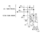
- FIG. 2 This is illustrated in FIG. 2 .
- the aggressor timing windows 201 and victim timing window 203 in the figure correspond to victim low to high transition and aggressor high to low transitions (see FIG. 1 ) and that the victim and aggressor driver node windows have been shifted to represent possible switching times relevant to input s 1 205 of the victim net 207 .
- the worst case impact due to these three aggressors is then found by finding the “right” alignment between the switching times of these four nets such that the delay impact or delta delay 211 on the victim net is maximized (some approaches try to maximize delay change at the victim sink, whereas others aim to maximize delay change at the victim sink output after the signal propagates). Note that, this amounts to enlarging the timing window associated with this net that will be used in a STA analysis. This delta delay is then back-annotated to the corresponding timing arc 213 in STA as shown. Once this operation is done for each net in the design, a STA update is performed to account for the impact of the back-annotated delta delays.
- the STA update results in new timing windows and noise analysis is repeated using these modified timing windows and iterations continue until the timing windows converge.
- the corresponding delta delay value is chosen depending on the type of timing check being employed. For example for a setup analysis, the delta delays are utilized such that the launch clock and signal path delay are increased whereas the capture clock delay is decreased.
- FIG. 3 a simplified and representative functional diagram of a system 300 and methodology for reducing pessimism, i.e. reducing false timing indications or problems, in or resulting from a crosstalk noise aware static timing analysis will be discussed and described.
- the system and methodology of FIG. 2 utilize a STA analysis engine that is, as known and not specifically depicted, provided with information regarding a semiconductor integrated circuit layout including an interconnect system as well as modeled grounded capacitances and series resistors. Further provided is a circuit description and timing library corresponding to various circuit cells that are utilized. Also various timing constraints and the like user inputs are provided.
- the STA analysis engine operates as generally described above.
- the STA engine provides static timing windows and transition times for the various nets and nodes in the interconnect system to a noise analysis function 303 .
- the noise analysis function 303 is also provided with IC layout information with various parasitic capacitors modeled for respective nets, circuit description, and noise viewpoint libraries (not specifically depicted).
- the noise analysis function includes a crosstalk noise induced delay calculation process 305 that operates in accordance with the discussions above with reference to FIG. 2 .
- a novel effective delta delay function (module or program) 307 Further included and inter coupled to the induced delay calculation process 305 is a novel effective delta delay function (module or program) 307 .
- the effective delta delay function 307 determines effective delay noise or delta delays due to crosstalk noise, utilizing timing windows and a net by net delay noise analysis technique, however the timing windows are used in an inventive manner.
- victim and aggressor timing windows and their overlap properties are used such that for each victim net, only the contribution of delta delay that impacts the early and late arrival times at the path endpoints is taken into account (effective delta delay). This is further described below in detail with examples and the like.
- the effective delta delays are then back-annotated 309 , timing windows are enlarged accordingly and the STA engine may do one or more additional iterations, depending on when or the extent to which resultant timing windows may be changing. The result is a listing or indication of problem or failing paths due to failure to meet timing constraints.
- the method implemented is one of reducing false timing problems resulting from pessimism in noise aware static timing analysis.
- the method initially or first performs noise aware static timing analysis using effective delay noise calculations on an interconnect system to identify failing paths corresponding to the semiconductor interconnect system.
- the performing noise aware static timing analysis using effective delay noise calculations further comprises determining one or more effective adjustments to respective timing windows for corresponding victim nets based on when, within the respective timing window an action of one or more aggressors occurs.
- This may further comprise iteratively performing noise aware static timing analysis augmented with effective delay noise analysis using adjusted timing windows corresponding to the effective adjustments to respective timing windows. Note the number of failing paths will be significantly smaller than in the analysis process described above with reference to FIG. 2 , however these paths may still include undue pessimism.
- the path based delay noise analysis 311 is a path based method in contrast to the typical net based method. In this approach, the analysis is done on one signal path at a time. The process at 311 can extract critical paths or process all paths depending on resources that are available and the like.
- the path based approach essentially eliminates the timing window for the victim that results from multiple paths traversing the same net and thus allows analysis with a deterministic switching time which reduces pessimism significantly.
- One difficulty in this approach is the necessity of a global optimization on the entire path. For example a worst case situation of switching all possible aggressors on one net of the path or victim path, may not guarantee a worst case delay impact on the overall path.
- the module or process 311 performs path based delay noise analysis on a plurality of the failing paths to eliminate false failing paths corresponding to at least a portion of the failing paths identified with the effective delta delay process.
- the process of performing path based delay noise analysis further comprises determining a switching time window for a victim, where the switching time window is determined for and uniquely corresponds to a particular path through the victim.
- the performing path based delay noise analysis advantageously further comprises determining an uncertainty in the switching time window based on when within the switching time window an action of one or more aggressors occurs.
- the system and methodology of FIG. 3 can be advantageously embodied in a software program comprising software instructions that when executed by a computer result in the performing the noise aware static timing analysis using effective delay noise and the performing the path based delay noise analysis.
- FIG. 4 a diagram that illustrates an exemplary determination of effective delta delay will be discussed and described. Note that this exemplifies the process that can be employed in the FIG. 3 system and shows the same situation for the same victim as illustrated in FIG. 2 , i.e. with the aggressor timing windows 201 and victim timing window 203 where all timing windows overlap in the region 209 .
- the final step of static timing analysis is to obtain the early and late arrival times at the timing check points, and compare them with the required times at these points. Therefore, what one should worry about in noise aware STA is the actual impact of crosstalk induced delay to the early and late arrival times.
- the effective delta delay technique is driven by this observation. Referring to FIG. 4 , the three aggressor nets (timing windows 301 , 303 , 305 and the victim net (timing window 203 starting at boundary 307 and ending at boundary 309 ) can switch together in the first over lapping region 209 resulting in all three aggressors possibly impacting the delay of the victim net in a worst case manner.
- the latest time point or boundary around which these nets should switch to be able to realize this impact on the victim net is t 1 311 .
- the path in which the victim net is switching around time t 1 is the latest path through this net that can be impacted by all three aggressors. If the delta_delay 312 due to these three aggressors is dd 1 , then the switching time of the victim net will be delayed to t 1 +dd 1 . Furthermore, only if t 1 +dd 1 >t 3 309 (end of the victim timing window 203 ), will this have an impact on the late arrival point of the victim net timing window by the amount t 1 +dd 1 ⁇ t 3 .
- the effective delta delay which is the maximum impact of all possible scenarios to the late arrival time of the timing window is given by an expression, i.e. maximum over i of (ti+ddi ⁇ tend): (max)
- the method of reducing pessimism in cross talk noise aware static timing analysis discussed above includes providing a victim timing window 203 corresponding to a victim and providing at least one aggressor timing window ( 3 depicted 301 , 303 , 305 ) corresponding to at least one aggressor. Then comparing the victim timing window with the aggressor timing windows to identify overlapping regions 209 , 319 , 321 and determining an impact on victim timing (delta delay) of an action, e.g. switching, by the at least one aggressor that occurs during the overlapping region and determining an effective delta delay corresponding to any portion of the impact on victim timing that extends beyond the victim timing window (see expression above for effective delta delay. Given the effective delta delay the method further adjusts the victim timing window to include the effective delta delay to provide an adjusted victim timing window.
- the method of determining the effective delta delay generally comprises adding the impact to a boundary of the overlapping region and subtracting a boundary of the victim timing window to provide the effective delta delay, e.g. t 1 +dd 1 ⁇ tend.
- adjusting the victim timing window to include the effective delta delay to provide an adjusted victim timing window enlarges the adjusted victim timing window and increases a late arrival time of paths through the victim.
- the adjusting the victim timing window to include the effective delta delay to provide an adjusted victim timing window enlarges the adjusted victim timing window and reduces an early arrival time of paths through the victim when early arrival times are being analyzed or evaluated. Given the adjusted victim timing window the remaining processes using the adjusted victim timing window can be repeated. Using this approach the number of false timing problem indications in a timing analysis of an interconnect system can be reduced.
- this method can be used when a plurality of aggressor timing windows corresponding respectively to a plurality of aggressors is provided.
- the victim timing window is compared with the plurality of aggressor timing windows to identify a plurality of overlapping regions, where each of the plurality of overlapping regions corresponds to one or more of the plurality of aggressor timing windows.
- the method determines a plurality of impacts delta delays on victim timing of or resulting from actions, e.g. switching by one or more of the plurality of aggressors corresponding to and occurring during each of the plurality of overlapping regions and selects as the effective delta delay the largest portion of the plurality of impacts on victim timing that extends beyond the victim timing window.
- the effective delta delay techniques are concerned with the delay noise impact on the min (early) and max (late) arrival time points on a net. This approach assumes that the timing paths that correspond to these min and max arrival times propagate to the end points where final timing checks will be made. There can be situations where this technique encounters various timing exceptions (i.e., false and/or multicycle paths) in which case further refinements can be appropriate. Suppose that there are two paths -a-c-e 501 and -b-d-e 503 coming into the same endpoint e as shown in FIG. 5 .
- the timing windows 505 at a, b, c, d, e are also depicted.
- the -a-c-e path 501 is earlier than the -b-d-e path 503 , therefore making the -b-d-e path 503 the critical one of the two in case of a setup analysis. If we look at the contribution of the two paths to the timing window at e 507 , we can see that the -b-d-e path 503 is contributing to the later portion of this window 509 (bold region te 2 -te 3 ). If the paths through b to e, i.e.
- path based delay determination as may be performed in the FIG. 3 system will be described and discussed. Additional pessimism reduction in noise aware STA can be provided if the static nature of the above techniques are removed and a more dynamic or situation specific analysis is performed. Elimination of iterations may also be beneficial. This can be accomplished using path based delay determination, where the analysis is performed on a path by path basis instead of the net by net approaches described above. If we look at a timing path for setup analysis, it contains the launch clock path and the signal path. The arrival times on the nets for a particular path need not be represented as windows as they are deterministic, i.e. with a known starting point and conditions.
- FIG. 6 Another appealing property of path based delay noise analysis is that it allows noise-aware timing of a given path in a single pass, i.e. without iterations.
- One path based delay noise analysis, i.e. solution of realizing this iteration free computation is illustrated in FIG. 6 .
- the exemplary path or portion of a path 600 of FIG. 6 includes three gates 601 with intervening nets v 1 603 and v 2 605 . Since a particular path is being analyzed the switching point of net v 1 can be found to be a 1 607 which aligns with all three aggressors 609 at time a 1 . Suppose the noise induced delay pushes or delays this time by ddx 611 .
- v 2 605 As net v 2 605 is being analyzed, if we consider the hypothetical delay change ddx in v 1 the switching point of v 2 initially determined to be a 2 613 is first moved by ddx to tx 615 in scenario 1 612 . Now, v 2 aligns with none of its aggressors 616 as shown. However this approach to iteration-less analysis may not always be conservative.
- scenario 2 614 where for v 1 , only two of the possible three aggressors 609 switch and that this moves the switching point of v 1 603 by less than ddx 611 , e.g. ddy 617 . Now, v 2 605 will be shifted less, e.g.
- the graphs depict or facilitate a method of reducing pessimism in cross talk noise aware static timing analysis.
- the method may be utilized to reduce a number of false timing problem indications in a timing analysis of an interconnect system.
- the method includes providing at least one aggressor timing window 609 corresponding to at least one aggressor (three shown) and providing, for a victim, a switching time window for a path through the victim.
- the switching time window will include a switching time, e.g. a 1 607 as well as an uncertainty or uncertainty factor (see for example a 2 +u 1 625 ). This switching time window corresponds to a particular path and will vary with different paths.
- a switching time e.g. a 1 607 as well as an uncertainty or uncertainty factor (see for example a 2 +u 1 625 ).
- v 1 is the first net on the path 600 and thus the switching time window is a point in time a 1 607 .
- the method further includes determining an uncertainty u 1 627 in a switching time for the victim resulting from an action, e.g. switching logic levels, by the at least one aggressor or combination of actions by a combination of aggressors that occurs during the switching time window.
- the method may further comprise adding the uncertainty to the switching time a 1 for the victim net v 1 to provide an adjusted switching time window for the victim and thus the path through the victim. This is not specifically depicted but amounts to adding the uncertainty to the switching time for a subsequent victim net, e.g. v 2 as shown by a 2 +u 1 625 .
- the graphs 621 , 623 illustrate determining an uncertainty profile for respective nets v 1 603 , v 2 605 .
- Graph 621 assumes that v 1 it is the first net of the path (primary input or first net after clock source) and has a deterministic single switching point a 1 i.e. there is no uncertainty in switching time a 1 .
- the x and y axis represent the arrival time at the corresponding net, i.e. switching time for the net, with and without additional uncertainty at this stage, respectively.
- Corresponding aggressor timing windows that can impact the arrival time at this stage are also shown, e.g. aggressor timing windows 609 for v 1 and windows 616 for v 2 .
- the uncertainty 627 is the delta delay referenced to the switching time 629 that can be induced by all 3 aggressors.
- the highest and the lowest y-coordinates of this uncertainty profile is defined as the uncertainty at this stage, shown as u 1 627 on the y-axis.
- the no-noise arrival time and thus switching time at v 2 is a 2 613 .
- the upstream uncertainty u 1 627 is added to a 2 to represent the total uncertainty up to this point as shown in the x-axis as a 2 +u 1 625 .
- the uncertainty profile 631 of v 2 from a 2 to a 2 +u 1 is shown. From a 2 to t 1 633 the uncertainty is the delta delay from or due to 2 aggressors as shown and from t 1 to the lesser of t 2 635 or a 2 +u 1 , it is the delta delay from 1 aggressor.
- the uncertainty at this stage or net v 2 is again determined by the max and min y-coordinates of the uncertainty profile and represented as u 2 637 on the y-axis. If another net v 3 is present in the path u 2 would be added to the switching time a 3 for that net and an analogous analysis would occur. Thus this propagation continues until the path end point is reached.
- the uncertainty window on the victim path nets can only enlarge as the uncertainty is propagated down the path, taking into account all aggressor switching possibilities.
- the max point of the final uncertainty window obtained at the path end point gives the worst case arrival time for the path in one pass.
- An implementation of this technique requires very little overhead as the “uncertainty profile” information on each net is already generated as part of the traditional delay noise analysis when, for example a scan-line algorithm is used to obtain the worst case aggressor set.
- graph 621 shows providing, for a victim, a switching time window that comprises a point in time a 1 607 and the determining an uncertainty in victim switching time further comprises determining an uncertainty due to actions or switching of a plurality of aggressors at that point in time.
- the determining an uncertainty in victim switching time further comprises determining an uncertainty profile 629 , 631 from actions by one or more of a plurality of aggressors that occur during the switching time window and selecting as the uncertainty a maximum magnitude of the uncertainty profile.
- adding the uncertainty to a switching time for a subsequent victim provides a subsequent switching time window a 2 +u 1 for the path through the subsequent victim v 2 .
- adding the uncertainty to the switching time for the subsequent victim to provide the subsequent switching time window enlarges the subsequent switching time window and increases a late arrival time of the path through the subsequent victim.
- adding the uncertainty to the switching time for the subsequent victim to provide the subsequent switching time window enlarges the subsequent switching time window and reduces an early arrival time of the path through the subsequent victim.
- Another approach to maximizing the arrival times (late or early) when the victim is one of a plurality of victims comprising the path includes maximizing, using integer linear programming (ILP) techniques, an uncertainty in a last switching time for a last victim in the path. More particularly the following equations are solved.
- ILP integer linear programming
- the path of interest has “n” stages or nets, ti is arrival time of a signal on stage i of the path, dik is delta delay contribution from kth aggressor of stage i, di is the no-noise delay of stage i, and T is a very big number in this context.
- a timing window from Wsik to Weik represents the timing window of the kth aggressor net at the ith victim net on the path we are calculating.
- the integer-linear programming equations and inequalities when solved, will solve our optimization or maximization problem.
- Alpha_ik is 1 when ti is between Wsik and Weik, so it represents whether the victim switching time is intersecting the aggressor timing window and a_ik is 0 when alpha_ik is 0 and a_ik can be 0 or 1 when alpha_ik is one. So this variable represents whether to choose the kth aggressor to switch when it is possible to choose it.
- the inequality defines the relation between ti, Wsik, Weik and alpha_ik. For example when alpha_ik is 1, this says that ti is between Wsik and Weik. When alpha_ik is 0, this says that ti is between 0 and some big number.
- the design has been timing and functional crosstalk noise optimized. In other words, no timing violations without crosstalk induced delay noise, and no functional crosstalk noise violations (i.e., glitch noise) exist.
- TDN delay noise analysis
- EDN effective delay noise analysis
- PBDN path based delay noise analysis
Abstract
Description
(max)|i((ti+ddi−tend), EQ. 1
where ti is the latest possible impact time for over lapping region or scenario i, ddi is the crosstalk noise induced delay in scenario i and tend is the late arrival time of the victim net window. Note that a similar argument holds for delay decrease (early arrival time) cases. When compared to conventional delay noise analysis, this technique results in the back-annotation of
This is an integer-linear programming formulation of the optimization problem and can be solved with known techniques. The path of interest has “n” stages or nets, ti is arrival time of a signal on stage i of the path, dik is delta delay contribution from kth aggressor of stage i, di is the no-noise delay of stage i, and T is a very big number in this context. Suppose that a timing window from Wsik to Weik represents the timing window of the kth aggressor net at the ith victim net on the path we are calculating. The integer-linear programming equations and inequalities when solved, will solve our optimization or maximization problem.
Claims (22)
Priority Applications (1)
| Application Number | Priority Date | Filing Date | Title |
|---|---|---|---|
| US10/994,858 US7251797B2 (en) | 2004-11-22 | 2004-11-22 | Pessimism reduction in crosstalk noise aware static timing analysis |
Applications Claiming Priority (1)
| Application Number | Priority Date | Filing Date | Title |
|---|---|---|---|
| US10/994,858 US7251797B2 (en) | 2004-11-22 | 2004-11-22 | Pessimism reduction in crosstalk noise aware static timing analysis |
Publications (2)
| Publication Number | Publication Date |
|---|---|
| US20060112359A1 US20060112359A1 (en) | 2006-05-25 |
| US7251797B2 true US7251797B2 (en) | 2007-07-31 |
Family
ID=36462310
Family Applications (1)
| Application Number | Title | Priority Date | Filing Date |
|---|---|---|---|
| US10/994,858 Expired - Fee Related US7251797B2 (en) | 2004-11-22 | 2004-11-22 | Pessimism reduction in crosstalk noise aware static timing analysis |
Country Status (1)
| Country | Link |
|---|---|
| US (1) | US7251797B2 (en) |
Cited By (10)
| Publication number | Priority date | Publication date | Assignee | Title |
|---|---|---|---|---|
| WO2009035813A1 (en) * | 2007-09-14 | 2009-03-19 | International Business Machines Corporation | Method of constrained aggressor set selection for crosstalk induced noise |
| US20120137263A1 (en) * | 2010-11-29 | 2012-05-31 | International Business Machines Corporation | Timing closure in chip design |
| US8205181B1 (en) | 2010-03-05 | 2012-06-19 | Applied Micro Circuits Corporation | Victim net crosstalk reduction |
| US20120167030A1 (en) * | 2010-12-22 | 2012-06-28 | Advanced Micro Devices, Inc. | Method and apparatus for addressing and improving holds in logic networks |
| US8776003B2 (en) | 2012-07-31 | 2014-07-08 | Lsi Corporation | System and method for employing side transition times from signoff-quality timing analysis information to reduce leakage power in an electronic circuit and an electronic design automation tool incorporating the same |
| US20160070844A1 (en) * | 2014-09-08 | 2016-03-10 | Synopsys Inc. | Selectively reducing graph based analysis pessimism |
| US20160292344A1 (en) * | 2015-04-03 | 2016-10-06 | Mentor Graphics Corporation | Signal integrity delay utilizing a window bump-based aggressor alignment scheme |
| US20160378901A1 (en) * | 2015-06-23 | 2016-12-29 | International Business Machines Corporation | Applying random nets credit in an efficient static timing analysis |
| US10248753B2 (en) | 2016-10-07 | 2019-04-02 | International Business Machines Corporation | Pessimism reduction in hierarchical blockage aggressors using estimated resistor and capacitor values |
| TWI749497B (en) * | 2020-03-30 | 2021-12-11 | 創意電子股份有限公司 | Establishing method for timing model |
Families Citing this family (23)
| Publication number | Priority date | Publication date | Assignee | Title |
|---|---|---|---|---|
| US7191419B2 (en) * | 2004-07-22 | 2007-03-13 | International Business Machines Corporation | Method of timing model abstraction for circuits containing simultaneously switching internal signals |
| US7346867B2 (en) * | 2005-02-01 | 2008-03-18 | International Business Machines Corporation | Method for estimating propagation noise based on effective capacitance in an integrated circuit chip |
| US7523426B2 (en) | 2005-03-29 | 2009-04-21 | Lsi Corporation | Intelligent timing analysis and constraint generation GUI |
| US20080258755A1 (en) * | 2007-04-19 | 2008-10-23 | International Business Machines Incorporated | Noise Reduction Among Conductors |
| US7930675B2 (en) * | 2007-12-26 | 2011-04-19 | Cadence Design Systems, Inc. | Method and system for implementing timing analysis and optimization of an electronic design based upon extended regions of analysis |
| US8086978B2 (en) * | 2008-06-20 | 2011-12-27 | Cadence Design Systems, Inc. | Method and system for performing statistical leakage characterization, analysis, and modeling |
| US20100050144A1 (en) * | 2008-08-25 | 2010-02-25 | Lsi Corporation | System and method for employing signoff-quality timing analysis information to reduce leakage power in an electronic circuit and electronic design automation tool incorporating the same |
| US8069432B2 (en) * | 2008-09-30 | 2011-11-29 | Cadence Design Systems, Inc. | Method and system for performing statistical leakage characterization, analysis, and modeling |
| US8086983B2 (en) * | 2008-09-30 | 2011-12-27 | Cadence Design Systems, Inc. | Method and system for performing improved timing window analysis |
| US20100153897A1 (en) * | 2008-12-11 | 2010-06-17 | Lsi Corporation | System and method for employing signoff-quality timing analysis information concurrently in multiple scenarios to reduce leakage power in an electronic circuit and electronic design automation tool incorporating the same |
| US8219952B2 (en) * | 2009-02-23 | 2012-07-10 | Synopsys, Inc. | Variation aware victim and aggressor timing overlap detection by pessimism reduction based on relative positions of timing windows |
| JP5287540B2 (en) * | 2009-06-24 | 2013-09-11 | 富士通株式会社 | Circuit design apparatus and circuit design program |
| US8650513B2 (en) * | 2010-09-20 | 2014-02-11 | Synopsys, Inc. | Reducing x-pessimism in gate-level simulation and verification |
| US9141740B2 (en) | 2011-03-31 | 2015-09-22 | Cadence Design Systems, Inc. | Methods, systems, and articles of manufacture for implementing full-chip optimization with reduced physical design data |
| US8977998B1 (en) * | 2013-02-21 | 2015-03-10 | Altera Corporation | Timing analysis with end-of-life pessimism removal |
| US9026965B2 (en) | 2013-03-12 | 2015-05-05 | Synopsys, Inc. | Arrival edge usage in timing analysis |
| US9026978B1 (en) | 2013-10-24 | 2015-05-05 | Cadence Design Systems, Inc. | Reverse interface logic model for optimizing physical hierarchy under full chip constraint |
| US10394999B2 (en) | 2015-11-18 | 2019-08-27 | International Business Machines Corporation | Analysis of coupled noise for integrated circuit design |
| US9881123B1 (en) * | 2016-06-30 | 2018-01-30 | Cadence Design Systems, Inc. | Method and system for timing analysis with adaptive timing window optimization for determining signal integrity impact |
| US10565336B2 (en) | 2018-05-24 | 2020-02-18 | International Business Machines Corporation | Pessimism reduction in cross-talk noise determination used in integrated circuit design |
| US10726189B2 (en) | 2018-07-23 | 2020-07-28 | Sandisk Technologies Llc | Less-pessimistic static timing analysis for synchronous circuits |
| US11176301B2 (en) * | 2019-09-05 | 2021-11-16 | International Business Machines Corporation | Noise impact on function (NIOF) reduction for integrated circuit design |
| US11875099B2 (en) | 2021-08-09 | 2024-01-16 | International Business Machines Corporation | Noise impact on function (NIOF) reduction for integrated circuit design |
Citations (9)
| Publication number | Priority date | Publication date | Assignee | Title |
|---|---|---|---|---|
| US6405348B1 (en) | 1999-10-27 | 2002-06-11 | Synopsys, Inc. | Deep sub-micron static timing analysis in the presence of crosstalk |
| US6405350B1 (en) | 1997-07-18 | 2002-06-11 | Nec Corporation | System and method for improving crosstalk errors via the insertion of delay gates |
| US6414542B2 (en) | 1999-03-17 | 2002-07-02 | Koninklijke Philips Electronics N.V. | Integrated circuit with relative sense inversion of signals along adjacent parallel signal paths |
| US20020166101A1 (en) * | 2001-03-06 | 2002-11-07 | Nec Usa, Inc. | Crosstalk mitigation method and system |
| US6510540B1 (en) | 2000-08-17 | 2003-01-21 | International Business Machines Corporation | Windowing mechanism for reducing pessimism in cross-talk analysis of digital chips |
| US20030070150A1 (en) * | 2001-10-09 | 2003-04-10 | Allen Robert J. | Generation of refined switching windows in static timing analysis |
| US6587815B1 (en) | 2000-02-04 | 2003-07-01 | Sun Microsystems, Inc. | Windowing scheme for analyzing noise from multiple sources |
| US6615395B1 (en) | 1999-12-20 | 2003-09-02 | International Business Machines Corporation | Method for handling coupling effects in static timing analysis |
| US6665845B1 (en) | 2000-02-25 | 2003-12-16 | Sun Microsystems, Inc. | System and method for topology based noise estimation of submicron integrated circuit designs |
-
2004
- 2004-11-22 US US10/994,858 patent/US7251797B2/en not_active Expired - Fee Related
Patent Citations (11)
| Publication number | Priority date | Publication date | Assignee | Title |
|---|---|---|---|---|
| US6405350B1 (en) | 1997-07-18 | 2002-06-11 | Nec Corporation | System and method for improving crosstalk errors via the insertion of delay gates |
| US6414542B2 (en) | 1999-03-17 | 2002-07-02 | Koninklijke Philips Electronics N.V. | Integrated circuit with relative sense inversion of signals along adjacent parallel signal paths |
| US6405348B1 (en) | 1999-10-27 | 2002-06-11 | Synopsys, Inc. | Deep sub-micron static timing analysis in the presence of crosstalk |
| US6615395B1 (en) | 1999-12-20 | 2003-09-02 | International Business Machines Corporation | Method for handling coupling effects in static timing analysis |
| US6587815B1 (en) | 2000-02-04 | 2003-07-01 | Sun Microsystems, Inc. | Windowing scheme for analyzing noise from multiple sources |
| US6665845B1 (en) | 2000-02-25 | 2003-12-16 | Sun Microsystems, Inc. | System and method for topology based noise estimation of submicron integrated circuit designs |
| US6510540B1 (en) | 2000-08-17 | 2003-01-21 | International Business Machines Corporation | Windowing mechanism for reducing pessimism in cross-talk analysis of digital chips |
| US20020166101A1 (en) * | 2001-03-06 | 2002-11-07 | Nec Usa, Inc. | Crosstalk mitigation method and system |
| US6637014B2 (en) | 2001-03-06 | 2003-10-21 | Nec Corporation | Crosstalk mitigation method and system |
| US20030070150A1 (en) * | 2001-10-09 | 2003-04-10 | Allen Robert J. | Generation of refined switching windows in static timing analysis |
| US6651229B2 (en) | 2001-10-09 | 2003-11-18 | International Business Machines Corporation | Generation of refined switching windows in static timing analysis |
Cited By (18)
| Publication number | Priority date | Publication date | Assignee | Title |
|---|---|---|---|---|
| WO2009035813A1 (en) * | 2007-09-14 | 2009-03-19 | International Business Machines Corporation | Method of constrained aggressor set selection for crosstalk induced noise |
| US7685549B2 (en) | 2007-09-14 | 2010-03-23 | International Business Machines Corporation | Method of constrained aggressor set selection for crosstalk induced noise |
| CN101802783B (en) * | 2007-09-14 | 2013-08-14 | 国际商业机器公司 | Method of constrained aggressor set selection for crosstalk induced noise |
| US8205181B1 (en) | 2010-03-05 | 2012-06-19 | Applied Micro Circuits Corporation | Victim net crosstalk reduction |
| US20120137263A1 (en) * | 2010-11-29 | 2012-05-31 | International Business Machines Corporation | Timing closure in chip design |
| US8769470B2 (en) * | 2010-11-29 | 2014-07-01 | International Business Machines Corporation | Timing closure in chip design |
| US20120167030A1 (en) * | 2010-12-22 | 2012-06-28 | Advanced Micro Devices, Inc. | Method and apparatus for addressing and improving holds in logic networks |
| US8347250B2 (en) * | 2010-12-22 | 2013-01-01 | Advanced Micro Devices, Inc. | Method and apparatus for addressing and improving holds in logic networks |
| US8776003B2 (en) | 2012-07-31 | 2014-07-08 | Lsi Corporation | System and method for employing side transition times from signoff-quality timing analysis information to reduce leakage power in an electronic circuit and an electronic design automation tool incorporating the same |
| US20160070844A1 (en) * | 2014-09-08 | 2016-03-10 | Synopsys Inc. | Selectively reducing graph based analysis pessimism |
| US10354042B2 (en) * | 2014-09-08 | 2019-07-16 | Synopsys, Inc. | Selectively reducing graph based analysis pessimism |
| US20160292344A1 (en) * | 2015-04-03 | 2016-10-06 | Mentor Graphics Corporation | Signal integrity delay utilizing a window bump-based aggressor alignment scheme |
| US10325055B2 (en) * | 2015-04-03 | 2019-06-18 | Mentor Graphics Corporation | Signal integrity delay utilizing a window bump-based aggressor alignment scheme |
| US20160378901A1 (en) * | 2015-06-23 | 2016-12-29 | International Business Machines Corporation | Applying random nets credit in an efficient static timing analysis |
| US9836571B2 (en) * | 2015-06-23 | 2017-12-05 | International Business Machines Corporation | Applying random nets credit in an efficient static timing analysis |
| US10248753B2 (en) | 2016-10-07 | 2019-04-02 | International Business Machines Corporation | Pessimism reduction in hierarchical blockage aggressors using estimated resistor and capacitor values |
| US10552570B2 (en) | 2016-10-07 | 2020-02-04 | International Business Machines Corporation | Pessimism reduction in hierarchical blockage aggressors using estimated resistor and capacitor values |
| TWI749497B (en) * | 2020-03-30 | 2021-12-11 | 創意電子股份有限公司 | Establishing method for timing model |
Also Published As
| Publication number | Publication date |
|---|---|
| US20060112359A1 (en) | 2006-05-25 |
Similar Documents
| Publication | Publication Date | Title |
|---|---|---|
| US7251797B2 (en) | Pessimism reduction in crosstalk noise aware static timing analysis | |
| US7685549B2 (en) | Method of constrained aggressor set selection for crosstalk induced noise | |
| US7549134B1 (en) | Method and system for performing crosstalk analysis | |
| US7890904B2 (en) | Estimating jitter in a clock tree of a circuit and synthesizing a jitter-aware and skew-aware clock tree | |
| US20090055787A1 (en) | Generation of Engineering Change Order (ECO) Constraints For Use In Selecting ECO Repair Techniques | |
| US9881123B1 (en) | Method and system for timing analysis with adaptive timing window optimization for determining signal integrity impact | |
| US5553000A (en) | Eliminating retiming bottlenecks to improve performance of synchronous sequential VLSI circuits | |
| US8056035B2 (en) | Method and system for analyzing cross-talk coupling noise events in block-based statistical static timing | |
| US8316339B2 (en) | Zone-based leakage power optimization | |
| US20030188268A1 (en) | Low Vt transistor substitution in a semiconductor device | |
| US8549448B2 (en) | Delay optimization during circuit design at layout level | |
| US9064073B2 (en) | Hyper-concurrent optimization over multi-corner multi-mode scenarios | |
| US8359173B2 (en) | System and methods for dynamic power estimation for a digital circuit | |
| Papa et al. | RUMBLE: an incremental, timing-driven, physical-synthesis optimization algorithm | |
| Sze et al. | Path based buffer insertion | |
| Xiao et al. | Gate sizing to eliminate crosstalk induced timing violation | |
| US5966521A (en) | System and method for analyzing static timing | |
| KR100482894B1 (en) | How to Optimize Device Sizes in Semiconductor Devices | |
| US10956639B1 (en) | Method to reduce full-chip timing violation through time budgeting in integrated circuit design | |
| Ajami et al. | Post-layout timing-driven cell placement using an accurate net length model with movable steiner points | |
| JP2008020986A (en) | Crosstalk analyzing method | |
| Ahmadi et al. | A timing error mitigation technique for high performance designs | |
| US6990647B2 (en) | Variable stage ratio buffer insertion for noise optimization in a logic network | |
| Becer et al. | Pessimism reduction in crosstalk noise aware STA | |
| KR19980079812A (en) | How to optimize the circuit structure included in the circuit layout |
Legal Events
| Date | Code | Title | Description |
|---|---|---|---|
| AS | Assignment |
Owner name: FREESCALE SEMICONDUCTOR, INC., TEXAS Free format text: ASSIGNMENT OF ASSIGNORS INTEREST;ASSIGNORS:BECER, MURAT R.;ALGOR, ILAN;GRINSHPON, AMIR;AND OTHERS;REEL/FRAME:016405/0807;SIGNING DATES FROM 20050118 TO 20050131 |
|
| AS | Assignment |
Owner name: CITIBANK, N.A. AS COLLATERAL AGENT, NEW YORK Free format text: SECURITY AGREEMENT;ASSIGNORS:FREESCALE SEMICONDUCTOR, INC.;FREESCALE ACQUISITION CORPORATION;FREESCALE ACQUISITION HOLDINGS CORP.;AND OTHERS;REEL/FRAME:018855/0129 Effective date: 20061201 Owner name: CITIBANK, N.A. AS COLLATERAL AGENT,NEW YORK Free format text: SECURITY AGREEMENT;ASSIGNORS:FREESCALE SEMICONDUCTOR, INC.;FREESCALE ACQUISITION CORPORATION;FREESCALE ACQUISITION HOLDINGS CORP.;AND OTHERS;REEL/FRAME:018855/0129 Effective date: 20061201 |
|
| CC | Certificate of correction | ||
| AS | Assignment |
Owner name: CITIBANK, N.A., NEW YORK Free format text: SECURITY AGREEMENT;ASSIGNOR:FREESCALE SEMICONDUCTOR, INC.;REEL/FRAME:020518/0215 Effective date: 20071025 Owner name: CITIBANK, N.A.,NEW YORK Free format text: SECURITY AGREEMENT;ASSIGNOR:FREESCALE SEMICONDUCTOR, INC.;REEL/FRAME:020518/0215 Effective date: 20071025 |
|
| FEPP | Fee payment procedure |
Free format text: PAYOR NUMBER ASSIGNED (ORIGINAL EVENT CODE: ASPN); ENTITY STATUS OF PATENT OWNER: LARGE ENTITY |
|
| AS | Assignment |
Owner name: CITIBANK, N.A., AS COLLATERAL AGENT,NEW YORK Free format text: SECURITY AGREEMENT;ASSIGNOR:FREESCALE SEMICONDUCTOR, INC.;REEL/FRAME:024397/0001 Effective date: 20100413 Owner name: CITIBANK, N.A., AS COLLATERAL AGENT, NEW YORK Free format text: SECURITY AGREEMENT;ASSIGNOR:FREESCALE SEMICONDUCTOR, INC.;REEL/FRAME:024397/0001 Effective date: 20100413 |
|
| FPAY | Fee payment |
Year of fee payment: 4 |
|
| AS | Assignment |
Owner name: CITIBANK, N.A., AS NOTES COLLATERAL AGENT, NEW YOR Free format text: SECURITY AGREEMENT;ASSIGNOR:FREESCALE SEMICONDUCTOR, INC.;REEL/FRAME:030633/0424 Effective date: 20130521 |
|
| AS | Assignment |
Owner name: CITIBANK, N.A., AS NOTES COLLATERAL AGENT, NEW YOR Free format text: SECURITY AGREEMENT;ASSIGNOR:FREESCALE SEMICONDUCTOR, INC.;REEL/FRAME:031591/0266 Effective date: 20131101 |
|
| REMI | Maintenance fee reminder mailed | ||
| LAPS | Lapse for failure to pay maintenance fees | ||
| STCH | Information on status: patent discontinuation |
Free format text: PATENT EXPIRED DUE TO NONPAYMENT OF MAINTENANCE FEES UNDER 37 CFR 1.362 |
|
| FP | Lapsed due to failure to pay maintenance fee |
Effective date: 20150731 |
|
| AS | Assignment |
Owner name: FREESCALE SEMICONDUCTOR, INC., TEXAS Free format text: PATENT RELEASE;ASSIGNOR:CITIBANK, N.A., AS COLLATERAL AGENT;REEL/FRAME:037354/0225 Effective date: 20151207 Owner name: FREESCALE SEMICONDUCTOR, INC., TEXAS Free format text: PATENT RELEASE;ASSIGNOR:CITIBANK, N.A., AS COLLATERAL AGENT;REEL/FRAME:037356/0143 Effective date: 20151207 Owner name: FREESCALE SEMICONDUCTOR, INC., TEXAS Free format text: PATENT RELEASE;ASSIGNOR:CITIBANK, N.A., AS COLLATERAL AGENT;REEL/FRAME:037356/0553 Effective date: 20151207 Owner name: FREESCALE SEMICONDUCTOR, INC., TEXAS Free format text: PATENT RELEASE;ASSIGNOR:CITIBANK, N.A., AS COLLATERAL AGENT;REEL/FRAME:037354/0704 Effective date: 20151207 |
|
| AS | Assignment |
Owner name: MORGAN STANLEY SENIOR FUNDING, INC., MARYLAND Free format text: ASSIGNMENT AND ASSUMPTION OF SECURITY INTEREST IN PATENTS;ASSIGNOR:CITIBANK, N.A.;REEL/FRAME:037486/0517 Effective date: 20151207 |
|
| AS | Assignment |
Owner name: MORGAN STANLEY SENIOR FUNDING, INC., MARYLAND Free format text: ASSIGNMENT AND ASSUMPTION OF SECURITY INTEREST IN PATENTS;ASSIGNOR:CITIBANK, N.A.;REEL/FRAME:037518/0292 Effective date: 20151207 |
|
| AS | Assignment |
Owner name: NXP, B.V., F/K/A FREESCALE SEMICONDUCTOR, INC., NETHERLANDS Free format text: RELEASE BY SECURED PARTY;ASSIGNOR:MORGAN STANLEY SENIOR FUNDING, INC.;REEL/FRAME:040925/0001 Effective date: 20160912 Owner name: NXP, B.V., F/K/A FREESCALE SEMICONDUCTOR, INC., NE Free format text: RELEASE BY SECURED PARTY;ASSIGNOR:MORGAN STANLEY SENIOR FUNDING, INC.;REEL/FRAME:040925/0001 Effective date: 20160912 |
|
| AS | Assignment |
Owner name: NXP B.V., NETHERLANDS Free format text: RELEASE BY SECURED PARTY;ASSIGNOR:MORGAN STANLEY SENIOR FUNDING, INC.;REEL/FRAME:040928/0001 Effective date: 20160622 |
|
| AS | Assignment |
Owner name: MORGAN STANLEY SENIOR FUNDING, INC., MARYLAND Free format text: CORRECTIVE ASSIGNMENT TO CORRECT THE REMOVE PATENTS 8108266 AND 8062324 AND REPLACE THEM WITH 6108266 AND 8060324 PREVIOUSLY RECORDED ON REEL 037518 FRAME 0292. ASSIGNOR(S) HEREBY CONFIRMS THE ASSIGNMENT AND ASSUMPTION OF SECURITY INTEREST IN PATENTS;ASSIGNOR:CITIBANK, N.A.;REEL/FRAME:041703/0536 Effective date: 20151207 |
|
| AS | Assignment |
Owner name: SHENZHEN XINGUODU TECHNOLOGY CO., LTD., CHINA Free format text: CORRECTIVE ASSIGNMENT TO CORRECT THE TO CORRECT THE APPLICATION NO. FROM 13,883,290 TO 13,833,290 PREVIOUSLY RECORDED ON REEL 041703 FRAME 0536. ASSIGNOR(S) HEREBY CONFIRMS THE THE ASSIGNMENT AND ASSUMPTION OF SECURITYINTEREST IN PATENTS.;ASSIGNOR:MORGAN STANLEY SENIOR FUNDING, INC.;REEL/FRAME:048734/0001 Effective date: 20190217 |
|
| AS | Assignment |
Owner name: MORGAN STANLEY SENIOR FUNDING, INC., MARYLAND Free format text: CORRECTIVE ASSIGNMENT TO CORRECT THE REMOVE APPLICATION11759915 AND REPLACE IT WITH APPLICATION 11759935 PREVIOUSLY RECORDED ON REEL 037486 FRAME 0517. ASSIGNOR(S) HEREBY CONFIRMS THE ASSIGNMENT AND ASSUMPTION OF SECURITYINTEREST IN PATENTS;ASSIGNOR:CITIBANK, N.A.;REEL/FRAME:053547/0421 Effective date: 20151207 |
|
| AS | Assignment |
Owner name: NXP B.V., NETHERLANDS Free format text: CORRECTIVE ASSIGNMENT TO CORRECT THE REMOVEAPPLICATION 11759915 AND REPLACE IT WITH APPLICATION11759935 PREVIOUSLY RECORDED ON REEL 040928 FRAME 0001. ASSIGNOR(S) HEREBY CONFIRMS THE RELEASE OF SECURITYINTEREST;ASSIGNOR:MORGAN STANLEY SENIOR FUNDING, INC.;REEL/FRAME:052915/0001 Effective date: 20160622 |
|
| AS | Assignment |
Owner name: NXP, B.V. F/K/A FREESCALE SEMICONDUCTOR, INC., NETHERLANDS Free format text: CORRECTIVE ASSIGNMENT TO CORRECT THE REMOVEAPPLICATION 11759915 AND REPLACE IT WITH APPLICATION11759935 PREVIOUSLY RECORDED ON REEL 040925 FRAME 0001. ASSIGNOR(S) HEREBY CONFIRMS THE RELEASE OF SECURITYINTEREST;ASSIGNOR:MORGAN STANLEY SENIOR FUNDING, INC.;REEL/FRAME:052917/0001 Effective date: 20160912 |