US7157888B2 - Light loading control circuit for a buck-boost voltage converter - Google Patents
Light loading control circuit for a buck-boost voltage converter Download PDFInfo
- Publication number
- US7157888B2 US7157888B2 US11/160,036 US16003605A US7157888B2 US 7157888 B2 US7157888 B2 US 7157888B2 US 16003605 A US16003605 A US 16003605A US 7157888 B2 US7157888 B2 US 7157888B2
- Authority
- US
- United States
- Prior art keywords
- phase
- terminal
- switching unit
- circuit
- voltage
- Prior art date
- Legal status (The legal status is an assumption and is not a legal conclusion. Google has not performed a legal analysis and makes no representation as to the accuracy of the status listed.)
- Expired - Fee Related, expires
Links
Images


Classifications
-
- H—ELECTRICITY
- H02—GENERATION; CONVERSION OR DISTRIBUTION OF ELECTRIC POWER
- H02M—APPARATUS FOR CONVERSION BETWEEN AC AND AC, BETWEEN AC AND DC, OR BETWEEN DC AND DC, AND FOR USE WITH MAINS OR SIMILAR POWER SUPPLY SYSTEMS; CONVERSION OF DC OR AC INPUT POWER INTO SURGE OUTPUT POWER; CONTROL OR REGULATION THEREOF
- H02M3/00—Conversion of dc power input into dc power output
- H02M3/02—Conversion of dc power input into dc power output without intermediate conversion into ac
- H02M3/04—Conversion of dc power input into dc power output without intermediate conversion into ac by static converters
- H02M3/10—Conversion of dc power input into dc power output without intermediate conversion into ac by static converters using discharge tubes with control electrode or semiconductor devices with control electrode
- H02M3/145—Conversion of dc power input into dc power output without intermediate conversion into ac by static converters using discharge tubes with control electrode or semiconductor devices with control electrode using devices of a triode or transistor type requiring continuous application of a control signal
- H02M3/155—Conversion of dc power input into dc power output without intermediate conversion into ac by static converters using discharge tubes with control electrode or semiconductor devices with control electrode using devices of a triode or transistor type requiring continuous application of a control signal using semiconductor devices only
- H02M3/156—Conversion of dc power input into dc power output without intermediate conversion into ac by static converters using discharge tubes with control electrode or semiconductor devices with control electrode using devices of a triode or transistor type requiring continuous application of a control signal using semiconductor devices only with automatic control of output voltage or current, e.g. switching regulators
- H02M3/158—Conversion of dc power input into dc power output without intermediate conversion into ac by static converters using discharge tubes with control electrode or semiconductor devices with control electrode using devices of a triode or transistor type requiring continuous application of a control signal using semiconductor devices only with automatic control of output voltage or current, e.g. switching regulators including plural semiconductor devices as final control devices for a single load
- H02M3/1582—Buck-boost converters
-
- H—ELECTRICITY
- H02—GENERATION; CONVERSION OR DISTRIBUTION OF ELECTRIC POWER
- H02M—APPARATUS FOR CONVERSION BETWEEN AC AND AC, BETWEEN AC AND DC, OR BETWEEN DC AND DC, AND FOR USE WITH MAINS OR SIMILAR POWER SUPPLY SYSTEMS; CONVERSION OF DC OR AC INPUT POWER INTO SURGE OUTPUT POWER; CONTROL OR REGULATION THEREOF
- H02M3/00—Conversion of dc power input into dc power output
- H02M3/02—Conversion of dc power input into dc power output without intermediate conversion into ac
- H02M3/04—Conversion of dc power input into dc power output without intermediate conversion into ac by static converters
- H02M3/10—Conversion of dc power input into dc power output without intermediate conversion into ac by static converters using discharge tubes with control electrode or semiconductor devices with control electrode
- H02M3/145—Conversion of dc power input into dc power output without intermediate conversion into ac by static converters using discharge tubes with control electrode or semiconductor devices with control electrode using devices of a triode or transistor type requiring continuous application of a control signal
- H02M3/155—Conversion of dc power input into dc power output without intermediate conversion into ac by static converters using discharge tubes with control electrode or semiconductor devices with control electrode using devices of a triode or transistor type requiring continuous application of a control signal using semiconductor devices only
- H02M3/156—Conversion of dc power input into dc power output without intermediate conversion into ac by static converters using discharge tubes with control electrode or semiconductor devices with control electrode using devices of a triode or transistor type requiring continuous application of a control signal using semiconductor devices only with automatic control of output voltage or current, e.g. switching regulators
- H02M3/157—Conversion of dc power input into dc power output without intermediate conversion into ac by static converters using discharge tubes with control electrode or semiconductor devices with control electrode using devices of a triode or transistor type requiring continuous application of a control signal using semiconductor devices only with automatic control of output voltage or current, e.g. switching regulators with digital control
-
- H—ELECTRICITY
- H02—GENERATION; CONVERSION OR DISTRIBUTION OF ELECTRIC POWER
- H02M—APPARATUS FOR CONVERSION BETWEEN AC AND AC, BETWEEN AC AND DC, OR BETWEEN DC AND DC, AND FOR USE WITH MAINS OR SIMILAR POWER SUPPLY SYSTEMS; CONVERSION OF DC OR AC INPUT POWER INTO SURGE OUTPUT POWER; CONTROL OR REGULATION THEREOF
- H02M3/00—Conversion of dc power input into dc power output
- H02M3/02—Conversion of dc power input into dc power output without intermediate conversion into ac
- H02M3/04—Conversion of dc power input into dc power output without intermediate conversion into ac by static converters
- H02M3/10—Conversion of dc power input into dc power output without intermediate conversion into ac by static converters using discharge tubes with control electrode or semiconductor devices with control electrode
- H02M3/145—Conversion of dc power input into dc power output without intermediate conversion into ac by static converters using discharge tubes with control electrode or semiconductor devices with control electrode using devices of a triode or transistor type requiring continuous application of a control signal
- H02M3/155—Conversion of dc power input into dc power output without intermediate conversion into ac by static converters using discharge tubes with control electrode or semiconductor devices with control electrode using devices of a triode or transistor type requiring continuous application of a control signal using semiconductor devices only
- H02M3/156—Conversion of dc power input into dc power output without intermediate conversion into ac by static converters using discharge tubes with control electrode or semiconductor devices with control electrode using devices of a triode or transistor type requiring continuous application of a control signal using semiconductor devices only with automatic control of output voltage or current, e.g. switching regulators
- H02M3/158—Conversion of dc power input into dc power output without intermediate conversion into ac by static converters using discharge tubes with control electrode or semiconductor devices with control electrode using devices of a triode or transistor type requiring continuous application of a control signal using semiconductor devices only with automatic control of output voltage or current, e.g. switching regulators including plural semiconductor devices as final control devices for a single load
- H02M3/1588—Conversion of dc power input into dc power output without intermediate conversion into ac by static converters using discharge tubes with control electrode or semiconductor devices with control electrode using devices of a triode or transistor type requiring continuous application of a control signal using semiconductor devices only with automatic control of output voltage or current, e.g. switching regulators including plural semiconductor devices as final control devices for a single load comprising at least one synchronous rectifier element
-
- H—ELECTRICITY
- H02—GENERATION; CONVERSION OR DISTRIBUTION OF ELECTRIC POWER
- H02M—APPARATUS FOR CONVERSION BETWEEN AC AND AC, BETWEEN AC AND DC, OR BETWEEN DC AND DC, AND FOR USE WITH MAINS OR SIMILAR POWER SUPPLY SYSTEMS; CONVERSION OF DC OR AC INPUT POWER INTO SURGE OUTPUT POWER; CONTROL OR REGULATION THEREOF
- H02M1/00—Details of apparatus for conversion
- H02M1/0003—Details of control, feedback or regulation circuits
- H02M1/0032—Control circuits allowing low power mode operation, e.g. in standby mode
-
- Y—GENERAL TAGGING OF NEW TECHNOLOGICAL DEVELOPMENTS; GENERAL TAGGING OF CROSS-SECTIONAL TECHNOLOGIES SPANNING OVER SEVERAL SECTIONS OF THE IPC; TECHNICAL SUBJECTS COVERED BY FORMER USPC CROSS-REFERENCE ART COLLECTIONS [XRACs] AND DIGESTS
- Y02—TECHNOLOGIES OR APPLICATIONS FOR MITIGATION OR ADAPTATION AGAINST CLIMATE CHANGE
- Y02B—CLIMATE CHANGE MITIGATION TECHNOLOGIES RELATED TO BUILDINGS, e.g. HOUSING, HOUSE APPLIANCES OR RELATED END-USER APPLICATIONS
- Y02B70/00—Technologies for an efficient end-user side electric power management and consumption
- Y02B70/10—Technologies improving the efficiency by using switched-mode power supplies [SMPS], i.e. efficient power electronics conversion e.g. power factor correction or reduction of losses in power supplies or efficient standby modes
Definitions
- the present invention relates to a DC/DC voltage converter and, more particularly, to a light loading control circuit for a buck-boost voltage converter.
- FIG. 1 is a circuit diagram showing a conventional buck-boost voltage converter.
- the conventional buck-boost voltage converter includes a synchronous switching circuit 10 , a buck-boost control circuit 11 , a drive circuit 12 , and a light loading control circuit 13 .
- the buck-boost control circuit 111 generates a voltage conversion control signal VCS in accordance with a feedback of an output voltage V out .
- the drive circuit 12 In response to the voltage conversion control signal VCS, the drive circuit 12 generates four drive signals D 1 to D 4 for driving switching units S 1 to S 4 of the synchronous switching circuit 10 , respectively.
- an input voltage V in is effectively regulated to an output voltage V out regardless of the input voltage V in being higher than, equal to, or lower than the output voltage V out .
- types of the buck-boost control circuit 11 such as the circuits and methods disclosed in U.S. Pat. No. 6,166,527 and U.S. Pat. No. 6,788,033.
- the conventional buck-boost voltage converter enters an operation of a light loading mode for enhancing the efficiency in the voltage conversion.
- the drive circuit 12 is under control of the light loading control circuit 13 instead of responding to the voltage conversion control signal VCS of the buck-boost control circuit 11 .
- FIGS. 3 and 4 One example of the conventional light loading modes in the buck-boost voltage converter is disclosed in FIGS. 3 and 4 on page 10 of Datasheet LTC3440, entitled “Micropower Synchronous Buck-Boost DC/DC Converter,” published on year 2001 and by Linear Technology Corporation.
- FIG. 2(A) is a timing chart showing an inductor current I L in the conventional light loading mode.
- the conventional light loading mode has a rising phase and a falling phase.
- the inductor current I L linearly increases from zero to a peak current I pk .
- the inductor current I L linearly decreases from the peak current I pk to zero.
- FIG. 2(B) is a schematic diagram showing an operation state of the synchronous switching circuit 10 in the rising phase.
- the switching units S 1 and S 4 are turned ON and the switching units S 2 and S 3 are turned OFF, for coupling a first terminal La of an inductor L to the input voltage V in and coupling a second terminal Lb of the inductor L to a ground potential. Therefore, an inductor current I L linearly increases with a rate of V in /L.
- FIG. 2(C) is a schematic diagram showing an operation state of the synchronous switching circuit 10 in the falling phase.
- the switching units S 1 and S 4 are turned OFF and the switching units S 2 and S 3 are turned ON, for coupling the first terminal La to the ground potential and coupling the second terminal Lb to the output voltage V out . Therefore, the inductor current I L linearly decreases with a rate of V out /L.
- an average of the loading current I out is subjected to an upper limit, which may be calculated in accordance with the following equation (1):
- I out ⁇ _ ⁇ ave ⁇ ( max ) ( I pk 2 ) ⁇ ( V in V in + V out ) ( 1 )
- the conventional buck-boost voltage converter leaves the light loading mode and returns to the normal operation under the control of the buck-boost control circuit 11 .
- the buck-boost voltage converter regulates the input voltage V in into the output voltage V out . That is, the buck-boost voltage converter is applicable over a broad range of input voltages V in .
- a variation of the input voltage V in induces a change to the maximum average light loading current I out — ave(max) of the conventional light loading mode. More specifically, a partial derivative of the maximum average light loading current I out — ave(max) with respect to the input voltage V in may be expressed in the following equation (2):
- the light loading control circuit 13 commands the buck-boost voltage converter to leave the light loading mode in association with different maximum average light loading currents I out — ave(max) with respect to different input voltages V in .
- an object of the present invention is to provide a light loading control circuit capable of stably controlling activation and termination of a light loading mode of a buck-boost voltage converter over a broad range of input voltages.
- Another object of the present invention is to provide a light loading control circuit capable of suppressing influence to a maximum average light loading current induced by a variation of an input voltage.
- a light loading control circuit for controlling a switching circuit of a buck-boost voltage converter.
- the switching circuit has an input switching unit and an output switching unit.
- the input switching unit selectively couples a first terminal of an inductor to an input voltage and a ground potential.
- the output switching unit selectively couples a second terminal of the inductor to an output voltage and the ground potential.
- the light loading control circuit has a phase control unit and a sleep control unit.
- the phase control unit operates the switching circuit in a plurality of phase cycles. Each of the phase cycles has a rising phase, a falling phase, and a maintaining phase.
- the switching circuit In the rising phase, the switching circuit is operated to increase an inductor current flowing through the inductor. Alternatively, the switching circuit is operated to cause a potential difference across the first terminal and the second terminal to have a first polarity.
- the switching circuit is operated to decrease the inductor current.
- the switching circuit is operated to cause the potential difference across the first terminal and the second terminal to have a second polarity. The second polarity is opposite to the first polarity.
- the maintaining phase the switching circuit is operated to keep the inductor current approximately constant. Alternatively, the switching circuit is operated to cause the potential difference across the first terminal and the second terminal to substantially become zero.
- the sleep control unit After the output voltage reaches a predetermined sleep reference voltage, the sleep control unit operates the switching circuit in a sleep period for preventing the first terminals and the second terminals from being coupled to two selected from a group consisting of the input voltage, the output voltage, and the ground potential. In the sleep period, a loading current is supplied exclusively from a discharge of an output capacitor.
- the light loading control circuit according to the present invention stably control the activation and termination of the light loading mode of the buck-boost voltage converter.
- FIG. 1 is a circuit diagram showing a conventional buck-boost voltage converter
- FIG. 2(A) is a timing chart showing an inductor current in a conventional light loading mode
- FIG. 2(B) is a schematic diagram showing an operation state of a synchronous switching circuit in a rising phase
- FIG. 2(C) is a schematic diagram showing an operation state of a synchronous switching circuit in a falling phase
- FIG. 3 is a circuit diagram showing a buck-boost voltage converter according to a first embodiment of the present invention
- FIG. 4 is a timing chart showing a voltage feedback signal and an inductor current in a light loading mode according to a first embodiment of the present invention
- FIG. 5(A) is a schematic diagram showing an operation state of a synchronous switching circuit in a rising phase
- FIG. 5(B) is a schematic diagram showing an operation state of a synchronous switching circuit in a falling phase
- FIG. 5(C) is a schematic diagram showing an operation state of a synchronous switching circuit in a maintaining phase
- FIG. 5(D) is a schematic diagram showing six operation states of a synchronous switching circuit in a sleep period
- FIG. 6 is a detailed circuit diagram showing a maintenance time control unit according to a first embodiment of the present invention.
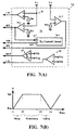
- FIG. 7(A) is a circuit diagram showing a light loading control circuit according to a second embodiment of the present invention.
- FIG. 7(B) is a timing chart showing an inductor current in the light loading mode according to a second embodiment of the present invention.
- FIG. 8(A) is a circuit diagram showing a light loading control circuit according to a third embodiment of the present invention.
- FIG. 8(B) is a timing chart showing an inductor current in the light loading mode according to a third embodiment of the present invention.
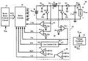
- FIG. 3 is a circuit diagram showing a buck-boost voltage converter according to a first embodiment of the present invention.
- the buck-boost voltage converter generates a regulated output voltage V out from an input voltage V in , which may be higher than, equal to, or lower than the output voltage V out .
- the buck-boost voltage converter includes a synchronous switching circuit 30 , a buck-boost control circuit 31 , a drive circuit 32 , a light loading control circuit 33 , and a voltage feedback circuit 34 .
- the synchronous switching circuit 30 has an input switching unit and an output switching unit. More specifically, the input switching unit is configured of a first switching unit S 1 and a second switching unit S 2 while the output switching unit is configured of a third switching unit S 3 and a fourth switching unit S 4 .
- the first switching unit S 1 is interposed between the input voltage V in and a first terminal La of an inductor L.
- the second switching unit S 2 is interposed between the first terminal La of the inductor L and a ground potential.
- the third switching unit S 3 is interposed between a second terminal Lb of the inductor L and the output voltage V out .
- the fourth switching unit S 4 is interposed between the second terminal Lb of the inductor L and the ground potential.
- the voltage feedback circuit 34 is coupled to generate a voltage feedback signal Vfb representative of the output voltage V out .
- the voltage feedback circuit 34 may be implemented by a voltage divider made up of a plurality of series-connected resistors.
- the buck-boost control circuit 31 In response to the voltage feedback signal V fb , the buck-boost control circuit 31 generates a voltage conversion control signal VCS for determining the ON/OFF time of the switching units S 1 to S 4 of the synchronous switching circuit 30 .
- the voltage conversion control signal VCS may include a plurality of component signals, independent or dependent with respect to each other, for individually controlling the switching units S 1 to S 4 .
- the drive circuit 32 four drive signals D 1 to D 4 are definitely formed in response to the voltage conversion control signal VCS, for respectively driving the switching units S 1 to S 4 .
- the input voltage V in is converted to the output voltage V out , regardless of the input voltage V in being higher than, equal to, or lower than the output voltage V out .
- the buck-boost control circuits 31 have been well-known to one skilled in the art, further descriptions are omitted hereinafter for the sake of simplicity. It should be noted that the present invention is directed to the light loading control circuit 33 , which may be applied to a variety of buck-boost voltage converters without any special limitations or system requirements.
- the buck-boost voltage converter enters an operation of a light loading mode for enhancing the efficiency in the voltage conversion.
- the drive circuit 32 is controlled by the light loading control circuit 33 instead of responding to the voltage conversion control signal VCS of the buck-boost control circuit 31 .
- the light loading control circuit 33 includes an activation unit 35 , a phase control unit 36 , a sleep control unit 37 , and a termination unit 38 .
- the activation unit 35 detects the inductor current I L and is triggered to generate a light loading activation signal LM as soon as the inductor current I L becomes lower than a predetermined threshold current I th .
- the drive circuit 32 is manipulated by the light loading control circuit 33 for performing a light loading mode with a higher efficiency.
- the activation unit 35 may be implemented by a current comparator for comparing the inductor current I L and the threshold current I th and being triggered to generate the light loading activation signal LM when the inductor current I L falls below the threshold current I th .
- the phase control unit 36 operates the synchronous switching circuit 30 in a plurality of phase cycles, each of which has a rising phase, a falling phase, and a maintaining phase.
- the inductor current I L linearly increases from a predetermined bottom current I bm to a predetermined peak current I pk .
- the inductor current I L linearly decreases from the peak current I pk to the bottom current I bm .
- the inductor current I L is kept approximately constant, i.e. at the bottom current I bm at time t 3 .
- the phase control unit 36 is installed with a current comparator 36 - 1 for comparing the inductor current I L and the peak current I pk . As soon as the inductor current I L linearly increases to reach the peak current I pk , the current comparator 36 - 1 is triggered to generate a rising termination signal RX for commanding the drive circuit 32 to terminate the operation of the rising phase of the synchronous switching circuit 30 .
- the phase control unit 36 is further installed with another current comparator 36 - 2 for comparing the inductor current I L and the bottom current I bm . As soon as the inductor current I L linearly decreases to reach the bottom current I bm , the current comparator 36 - 2 is triggered to generate a falling termination signal FX for commanding the drive circuit 32 to terminate the operation of the falling phase of the synchronous circuit 30 .
- the bottom current I bm may be set as a zero.
- the phase control unit 36 is further installed with a maintenance time control unit 36 - 3 for determining a maintenance time T m for which the maintaining phase lasts.
- the maintenance time control unit 36 - 3 has a trigger terminal AT and an output terminal AO.
- the trigger terminal AT receives the falling termination signal FX
- the maintenance time control unit 36 - 3 starts counting the time.
- the output terminal AO of the maintenance time control unit 36 - 3 generates a maintaining termination signal MX for commanding the drive circuit 32 to terminate the operation of the maintaining phase of the synchronous switching circuit 30 .
- the switching units S 1 and S 4 are turned ON while the switching units S 2 and S 3 are turned OFF such that the first terminal La of the inductor L is coupled to the input voltage V in while the second terminal Lb of the inductor L is coupled to the ground potential.
- the inductor current I L linearly increases with a rate of V in /L.
- the switching units S 1 and S 4 are turned OFF while the switching units S 2 and S 3 are turned ON such that the first terminal La of the inductor L is coupled to the ground potential while the second terminal Lb of the inductor L is coupled to the output voltage V out .
- the inductor current I L linearly decreases with a rate of V out /L.
- the switching units S 1 and S 3 are turned OFF while the switching units S 2 and S 4 are turned ON such that the first and second terminals La and Lb of the inductor L are coupled to the ground potential. Since a potential difference across the first and second terminals La and Lb of the inductor L is rendered zero, the inductor current I L freely flows around a closed loop so as to maintain at an approximately constant state if finite resistances of the inductor L and the switching units S 2 and S 4 are neglected.
- the sleep control unit 37 is triggered to generate a sleep signal SLP at some time in the plurality of phase cycles when the voltage feedback signal V fb reaches a predetermined sleep reference voltage V sip .
- the drive circuit 32 operates the switching circuit 30 in a sleep period for preventing the first and second terminals La and Lb of the inductor L from being respectively coupled to two selected from a group consisting of the input voltage V in , the output voltage V out , and the ground potential.
- the synchronous switching circuit 30 in the sleep period may be operated in any one of six operation states Case 1 to Case 6 .
- the first switching unit S 1 is turned ON while the second to fourth switching units S 2 to S 4 are turned OFF such that the first terminal La of the inductor L is coupled to the input voltage V in while the second terminal Lb of the inductor L is floated.
- the second switching unit S 2 is turned ON while the first, third, and fourth switching units S 1 , S 3 , and S 4 are turned OFF such that the first terminal La of the inductor L is coupled to the ground potential while the second terminal Lb of the inductor L is floated.
- the third switching unit S 3 is turned ON while the first, second, and fourth switching units S 1 , S 2 , and S 4 are turned OFF such that the first terminal La of the inductor L is floated while the second terminal Lb of the inductor L is coupled to the output voltage V out .
- the fourth switching unit S 4 is turned ON while the first to third switching units S 1 to S 3 are turned OFF such that the first terminal La of the inductor L is floated while the second terminal Lb of the inductor L is coupled to the ground potential.
- the second and fourth switching units S 2 and S 4 are turned ON while the first and third switching units S 1 and S 3 are turned OFF such that the first and second terminals La and Lb of the inductor L are coupled to the ground potential.
- the first to fourth switching units S 1 to S 4 are turned OFF such that the first and second terminals La and Lb of the inductor L are floated.
- the sleep control unit 37 may be implemented by a hysteresis voltage comparator. From time t 5 to t 6 in FIG. 4 , the voltage feedback signal V fb drops by a predetermined hysteresis voltage V hys due to the discharge of the output capacitor C out . At time t 6 , the sleep period is terminated and the operation of the synchronous switching circuit 30 returns to the phase cycles controlled by the phase control unit 36 .
- the termination unit 38 In the light loading mode, if the maximum average light loading current I out — ave(max) cannot satisfies the requirement of the loading current I out , the termination unit 38 generates a light loading termination signal LX. In response to the light loading termination signal LX, the drive circuit 32 returns under the control of the buck-boost control circuit 31 for performing the general buck-boost voltage conversion.
- the termination unit 38 may be implemented by a voltage comparator for comparing the voltage feedback signal V fb and a predetermined threshold voltage V th . In the case where the maximum average light loading current I out — ave(max) cannot satisfies the requirement of the loading current I out , the voltage feedback signal V fb demonstrates a tendency to decrease in average.
- the threshold voltage V th is designed such that the voltage comparator of the termination unit 38 is triggered to generate the light loading termination signal LX as soon as the voltage feedback signal V fb decreases below the threshold voltage V th . It should be noted that the threshold voltage V th is set lower than the sleep reference voltage V sip minus the hysteresis voltage Vhys for ensuring that the desired function is correctly achieved.
- the maximum average light loading current I out — ave(max) may be calculated from the following equation (3):
- I out ⁇ _ ⁇ ave ⁇ ( max ) ( I pk 2 ) ⁇ ( V out ( 1 + T m ⁇ V out I pk ⁇ L ) ⁇ V in + V out ) ( 3 )
- the input voltage V in can be higher than, equal to, or lower than the output voltage V out . That is, the buck-boost voltage converter is applicable over a broad range of input voltages V in .
- a variation of the input voltage V in induces an influence to the maximum average light loading current I out — ave(max) .
- a partial derivative of the maximum average light loading current I out — ave(max) of equation (3) with respect to the input voltage V in may be expressed in the following equation (4):
- the light loading control circuit 33 stably controls the activation and termination of the light loading mode of the buck-boost voltage converter.
- the maintenance time T m is not limited to a constant but may be implemented by a controllable variable.
- the maximum average light loading current I out — ave(max) may be calculated by the following equation (6):
- I out ⁇ _ ⁇ ave ⁇ ( max ) ( I pk 2 ) ⁇ ( V in ( V out ⁇ k I pk ⁇ L ) ⁇ V in 2 + V in + V out ) ( 6 )
- V in I pk ⁇ L k ( 8 )
- the maximum average light loading current I out — ave(max) is prevented from being influenced by the variation of the input voltage V in . Therefore, if the proportional constant k is so selected as to locate the value of equation (8) in the middle of the operational range of the input voltage V in , the influence to the maximum average light loading current I out — ave(max) induced with respect to the variation of the input voltage V in is effectively suppressed.
- FIG. 6 is a detailed circuit diagram showing the maintenance time control unit 36 - 3 according to the first embodiment of the present invention.
- the maintenance time control unit 36 - 3 may include a voltage comparator CP m , a current source I m , a capacitor C m , an NMOS transistor S m , and a buffer inverter B m .
- the NMOS transistor S m has a gate electrode, serving as the trigger terminal AT of the maintenance time control unit 36 - 3 , for receiving the falling termination signal FX through the buffer inverter B m .
- the voltage comparator CP m has an output terminal, serving as the output terminal AO of the maintenance time control unit 36 - 3 , for providing the maintaining termination signal MX.
- the falling termination signal FX changes to a high level state from a low level state.
- the NMOS transistor S m is turned OFF such that the current source I m starts charging the capacitor C m .
- the voltage comparator CP m is triggered to cause the maintaining termination signal MX to change to a high level state from a low level state. Therefore, the maintenance time T m is determined by the maintenance time control unit 36 - 3 .
- FIG. 7(A) is a circuit diagram showing a light loading control circuit 73 according to a second embodiment of the present invention.
- the second embodiment is different from the first embodiment in that the maintenance time control unit 76 - 3 of the second embodiment is triggered by the rising termination signal RX to start counting the maintenance time T m . Therefore, in the light loading mode of the second embodiment, the maintaining phase occurs immediately after the rising phase.
- FIG. 7(B) in the rising phase from time t 1 to t 2 , the inductor current I L linearly increases from the bottom current I bm to the peak current I pk .
- the inductor current I L is kept approximately constant, i.e. at the peak current I pk at time t 2 .
- the inductor current I L linearly decreases from the peak current I pk to the bottom current I bm .
- FIG. 8(A) is a circuit diagram showing a light loading control circuit 83 according to a third embodiment of the present invention.
- the third embodiment is different from the first embodiment in that the maintenance time control unit 86 - 3 of the third embodiment has a first trigger terminal AT 1 and a second trigger terminal AT 2 and a first output terminal AO 1 and a second output terminal AO 2 .
- the first trigger terminal AT 1 is triggered by the rising termination signal RX so as to start counting a first maintenance time T m1 .
- the first output terminal AO 1 outputs a first maintaining termination signal MX 1 . Therefore, in the light loading mode of the third embodiment, the first maintaining phase occurs immediately after the rising phase.
- the second trigger terminal AT 2 is triggered by the falling termination signal FX so as to start counting a second maintenance time T m2 .
- the second output terminal AO 2 outputs a second maintaining termination signal MX 2 . Therefore, in the light loading mode of the third embodiment, the second maintaining phase occurs immediately after the falling phase.
- the inductor current I L linearly increases from the bottom current I bm to the peak current I pk .
- the inductor current I L is kept approximately constant, i.e. at the peak current I pk at time t 2 .
- the inductor current I L linearly decreases from the peak current I pk to the bottom current I bm .
- the inductor current I L is kept approximately constant, i.e. at the bottom current I bm at time t 4 .
Abstract
Description
T m =k·V in (5)
Claims (20)
Priority Applications (1)
| Application Number | Priority Date | Filing Date | Title |
|---|---|---|---|
| US11/160,036 US7157888B2 (en) | 2005-06-06 | 2005-06-06 | Light loading control circuit for a buck-boost voltage converter |
Applications Claiming Priority (1)
| Application Number | Priority Date | Filing Date | Title |
|---|---|---|---|
| US11/160,036 US7157888B2 (en) | 2005-06-06 | 2005-06-06 | Light loading control circuit for a buck-boost voltage converter |
Publications (2)
| Publication Number | Publication Date |
|---|---|
| US20060273768A1 US20060273768A1 (en) | 2006-12-07 |
| US7157888B2 true US7157888B2 (en) | 2007-01-02 |
Family
ID=37493512
Family Applications (1)
| Application Number | Title | Priority Date | Filing Date |
|---|---|---|---|
| US11/160,036 Expired - Fee Related US7157888B2 (en) | 2005-06-06 | 2005-06-06 | Light loading control circuit for a buck-boost voltage converter |
Country Status (1)
| Country | Link |
|---|---|
| US (1) | US7157888B2 (en) |
Cited By (75)
| Publication number | Priority date | Publication date | Assignee | Title |
|---|---|---|---|---|
| US20060113975A1 (en) * | 2004-11-29 | 2006-06-01 | Supertex, Inc. | Method and apparatus for controlling output current of a cascaded DC/DC converter |
| US20070075687A1 (en) * | 2005-09-30 | 2007-04-05 | Takuya Ishii | Buck-boost converter |
| US20070290667A1 (en) * | 2006-06-16 | 2007-12-20 | Fujitsu Limited | Step-up/step-down type DC-DC converter, and control circuit and control method of the same |
| US20080001587A1 (en) * | 2006-06-30 | 2008-01-03 | Analog Devices, Inc. | DC to DC voltage converter |
| US7391190B1 (en) * | 2006-04-03 | 2008-06-24 | National Semiconductor Corporation | Apparatus and method for three-phase buck-boost regulation |
| US20090015229A1 (en) * | 2007-07-14 | 2009-01-15 | Kotikalapoodi Sridhar V | Bi-directional DC power converter |
| US7495419B1 (en) * | 2006-04-03 | 2009-02-24 | National Semiconductor Corporation | Apparatus and method for PFM buck-or-boost converter with smooth transition between modes |
| US20090085540A1 (en) * | 2007-01-22 | 2009-04-02 | Junji Nishida | Voltage Rising/Falling Type Switching Regulator and Reverse Current Prevention Method |
| US20090146623A1 (en) * | 2007-12-11 | 2009-06-11 | Analog Devices, Inc. | DC to DC converter |
| US7570033B1 (en) * | 2006-04-03 | 2009-08-04 | National Semiconductor Corporation | Apparatus and method for PWM buck-or-boost converter with smooth transition between modes |
| US20090208824A1 (en) * | 2008-02-15 | 2009-08-20 | Apple, Inc. | Power source having a parallel cell topology |
| US20090289603A1 (en) * | 2008-05-21 | 2009-11-26 | Apple Inc. | Method and apparatus for maintaining a battery in a partially charged state |
| US20090303755A1 (en) * | 2008-06-04 | 2009-12-10 | Novatek Microelectronics Corp. | Power converter apparatus |
| US20090310385A1 (en) * | 2008-06-13 | 2009-12-17 | Dragan Maksimovic | Method, apparatus & system for extended switched-mode controller |
| US20100156374A1 (en) * | 2008-04-16 | 2010-06-24 | Lopata Douglas D | Power Converter with Power Switch Operable in Controlled Current Mode |
| US20100164449A1 (en) * | 2008-12-29 | 2010-07-01 | Mirmira Ramarao Dwarakanath | Power Converter with a Dynamically Configurable Controller and Output Filter |
| US20100164650A1 (en) * | 2008-12-29 | 2010-07-01 | Ahmed Mohamed Abou-Alfotouh | Power Converter with a Dynamically Configurable Controller and Output Filter |
| US20100226194A1 (en) * | 2007-07-20 | 2010-09-09 | He Huang | Power-failure protection circuit for non-volatile semiconductor storage devices and method for preventing unexpected power-failure using the same |
| US7808217B2 (en) | 2007-10-18 | 2010-10-05 | Analog Devices, Inc. | DC to DC converter |
| US20100270986A1 (en) * | 2005-06-10 | 2010-10-28 | Selex Communications S.P.A. | High efficiency power converter, and modulator and transmitter using it |
| US20110012570A1 (en) * | 2009-07-14 | 2011-01-20 | Richtek Technology Corporation | Synchronous driver circuit and integrated circuit for use therein |
| US20110057724A1 (en) * | 2009-08-28 | 2011-03-10 | Pabon Gus Charles | High- and Low-Power Power Supply with Standby Power Saving Features |
| US20110074360A1 (en) * | 2009-09-30 | 2011-03-31 | Apple Inc. | Power adapter with internal battery |
| US20110074434A1 (en) * | 2009-09-30 | 2011-03-31 | Apple Inc. | End of life detection for a battery |
| US20110095742A1 (en) * | 2008-04-16 | 2011-04-28 | Douglas Dean Lopata | Power Converter with Controller Operable in Selected Modes of Operation |
| US20110101934A1 (en) * | 2008-04-16 | 2011-05-05 | Douglas Dean Lopata | Power Converter with Controller Operable in Selected Modes of Operation |
| US20110101933A1 (en) * | 2008-04-16 | 2011-05-05 | Douglas Dean Lopata | Power Converter with Controller Operable in Selected Modes of Operation |
| US20110101949A1 (en) * | 2008-04-16 | 2011-05-05 | Douglas Dean Lopata | Power Converter with Controller Operable in Selected Modes of Operation |
| US20110101948A1 (en) * | 2008-04-16 | 2011-05-05 | Douglas Dean Lopata | Power Converter with Controller Operable in Selected Modes of Operation |
| US20110148373A1 (en) * | 2009-12-18 | 2011-06-23 | Linear Technology Corporation | Continuously switching buck-boost control |
| US8063625B2 (en) | 2008-06-18 | 2011-11-22 | Apple Inc. | Momentarily enabled electronic device |
| US8077490B1 (en) * | 2007-03-16 | 2011-12-13 | Maxim Integrated Products, Inc. | Limit-cycle oscillation (LCO) generation by altering a digital transfer function of a feedback loop element |
| US20120248863A1 (en) * | 2006-12-06 | 2012-10-04 | Solaredge Technologies Ltd. | Safety Mechanisms, Wake Up and Shutdown Methods in Distributed Power Installations |
| US8519564B2 (en) | 2010-05-12 | 2013-08-27 | Apple Inc. | Multi-output power supply |
| US8867295B2 (en) | 2010-12-17 | 2014-10-21 | Enpirion, Inc. | Power converter for a memory module |
| US9509217B2 (en) | 2015-04-20 | 2016-11-29 | Altera Corporation | Asymmetric power flow controller for a power converter and method of operating the same |
| US20160365790A1 (en) * | 2015-06-15 | 2016-12-15 | Futurewei Technologies, Inc. | Control Method for Buck-Boost Power Converters |
| US9595871B1 (en) * | 2015-12-21 | 2017-03-14 | Texas Instruments Deutschland Gmbh | High efficiency inductive capacitive DC-DC converter |
| US20170077815A1 (en) * | 2015-09-10 | 2017-03-16 | Futurewei Technologies, Inc. | Control Method for Zero Voltage Switching Buck-Boost Power Converters |
| US9859796B2 (en) | 2014-06-10 | 2018-01-02 | Samsung Electronics Co., Ltd. | Buck-boost converter and operating method |
| US20180262098A1 (en) * | 2017-03-13 | 2018-09-13 | Rohm Co., Ltd. | Step-up/down dc-dc converter |
| US10396662B2 (en) | 2011-09-12 | 2019-08-27 | Solaredge Technologies Ltd | Direct current link circuit |
| US10447150B2 (en) | 2006-12-06 | 2019-10-15 | Solaredge Technologies Ltd. | Distributed power harvesting systems using DC power sources |
| US10468878B2 (en) | 2008-05-05 | 2019-11-05 | Solaredge Technologies Ltd. | Direct current power combiner |
| US10516336B2 (en) | 2007-08-06 | 2019-12-24 | Solaredge Technologies Ltd. | Digital average input current control in power converter |
| US10608553B2 (en) | 2012-01-30 | 2020-03-31 | Solaredge Technologies Ltd. | Maximizing power in a photovoltaic distributed power system |
| US10637393B2 (en) | 2006-12-06 | 2020-04-28 | Solaredge Technologies Ltd. | Distributed power harvesting systems using DC power sources |
| US10644589B2 (en) | 2007-12-05 | 2020-05-05 | Solaredge Technologies Ltd. | Parallel connected inverters |
| US10666125B2 (en) | 2011-01-12 | 2020-05-26 | Solaredge Technologies Ltd. | Serially connected inverters |
| US10673229B2 (en) | 2010-11-09 | 2020-06-02 | Solaredge Technologies Ltd. | Arc detection and prevention in a power generation system |
| US10673253B2 (en) | 2006-12-06 | 2020-06-02 | Solaredge Technologies Ltd. | Battery power delivery module |
| US10673222B2 (en) | 2010-11-09 | 2020-06-02 | Solaredge Technologies Ltd. | Arc detection and prevention in a power generation system |
| US10778025B2 (en) | 2013-03-14 | 2020-09-15 | Solaredge Technologies Ltd. | Method and apparatus for storing and depleting energy |
| US10931228B2 (en) | 2010-11-09 | 2021-02-23 | Solaredge Technologies Ftd. | Arc detection and prevention in a power generation system |
| US10931119B2 (en) | 2012-01-11 | 2021-02-23 | Solaredge Technologies Ltd. | Photovoltaic module |
| US10992238B2 (en) | 2012-01-30 | 2021-04-27 | Solaredge Technologies Ltd. | Maximizing power in a photovoltaic distributed power system |
| US11002774B2 (en) | 2006-12-06 | 2021-05-11 | Solaredge Technologies Ltd. | Monitoring of distributed power harvesting systems using DC power sources |
| US11018623B2 (en) | 2016-04-05 | 2021-05-25 | Solaredge Technologies Ltd. | Safety switch for photovoltaic systems |
| US11031861B2 (en) | 2006-12-06 | 2021-06-08 | Solaredge Technologies Ltd. | System and method for protection during inverter shutdown in distributed power installations |
| US11063440B2 (en) | 2006-12-06 | 2021-07-13 | Solaredge Technologies Ltd. | Method for distributed power harvesting using DC power sources |
| US11177663B2 (en) | 2016-04-05 | 2021-11-16 | Solaredge Technologies Ltd. | Chain of power devices |
| US11183968B2 (en) | 2012-01-30 | 2021-11-23 | Solaredge Technologies Ltd. | Photovoltaic panel circuitry |
| US11183969B2 (en) | 2007-12-05 | 2021-11-23 | Solaredge Technologies Ltd. | Testing of a photovoltaic panel |
| US11264947B2 (en) | 2007-12-05 | 2022-03-01 | Solaredge Technologies Ltd. | Testing of a photovoltaic panel |
| US11296650B2 (en) | 2006-12-06 | 2022-04-05 | Solaredge Technologies Ltd. | System and method for protection during inverter shutdown in distributed power installations |
| US11309832B2 (en) | 2006-12-06 | 2022-04-19 | Solaredge Technologies Ltd. | Distributed power harvesting systems using DC power sources |
| US11569660B2 (en) | 2006-12-06 | 2023-01-31 | Solaredge Technologies Ltd. | Distributed power harvesting systems using DC power sources |
| US11569659B2 (en) | 2006-12-06 | 2023-01-31 | Solaredge Technologies Ltd. | Distributed power harvesting systems using DC power sources |
| US11687112B2 (en) | 2006-12-06 | 2023-06-27 | Solaredge Technologies Ltd. | Distributed power harvesting systems using DC power sources |
| US11728768B2 (en) | 2006-12-06 | 2023-08-15 | Solaredge Technologies Ltd. | Pairing of components in a direct current distributed power generation system |
| US11735910B2 (en) | 2006-12-06 | 2023-08-22 | Solaredge Technologies Ltd. | Distributed power system using direct current power sources |
| US11855231B2 (en) | 2006-12-06 | 2023-12-26 | Solaredge Technologies Ltd. | Distributed power harvesting systems using DC power sources |
| US11867729B2 (en) | 2009-05-26 | 2024-01-09 | Solaredge Technologies Ltd. | Theft detection and prevention in a power generation system |
| US11881814B2 (en) | 2005-12-05 | 2024-01-23 | Solaredge Technologies Ltd. | Testing of a photovoltaic panel |
| US11888387B2 (en) | 2006-12-06 | 2024-01-30 | Solaredge Technologies Ltd. | Safety mechanisms, wake up and shutdown methods in distributed power installations |
Families Citing this family (18)
| Publication number | Priority date | Publication date | Assignee | Title |
|---|---|---|---|---|
| DE102004031395A1 (en) * | 2004-06-29 | 2006-02-02 | Infineon Technologies Ag | DC converter |
| JP5011874B2 (en) * | 2006-07-31 | 2012-08-29 | ミツミ電機株式会社 | Bi-directional converter and electronic device |
| EP2028753B1 (en) * | 2007-08-22 | 2012-06-27 | Maxim Integrated Products, Inc. | Step-up/step-down (Buck/Boost) switching regulator control methods |
| US7995359B2 (en) * | 2009-02-05 | 2011-08-09 | Power Integrations, Inc. | Method and apparatus for implementing an unregulated dormant mode with an event counter in a power converter |
| EP2144355B1 (en) * | 2008-07-07 | 2011-10-26 | ST-Ericsson SA | Voltage converter |
| US8085005B2 (en) * | 2009-06-18 | 2011-12-27 | Micrel, Inc. | Buck-boost converter with sample and hold circuit in current loop |
| US8860385B2 (en) * | 2011-01-30 | 2014-10-14 | The Boeing Company | Voltage controlled current source for voltage regulation |
| TWI463778B (en) * | 2011-04-29 | 2014-12-01 | Energy Pass Inc | Current mode buck-boost converter and direct current voltage converting method thereof |
| US9088211B2 (en) * | 2013-02-14 | 2015-07-21 | Texas Instruments Incorporated | Buck-boost converter with buck-boost transition switching control |
| US9978862B2 (en) | 2013-04-30 | 2018-05-22 | Infineon Technologies Austria Ag | Power transistor with at least partially integrated driver stage |
| US9799643B2 (en) | 2013-05-23 | 2017-10-24 | Infineon Technologies Austria Ag | Gate voltage control for III-nitride transistors |
| US9899923B2 (en) * | 2013-12-12 | 2018-02-20 | Infineon Technologies Austria Ag | Efficient PFM switch control for non-inverting buck-boost converter |
| US20160078842A1 (en) * | 2014-09-11 | 2016-03-17 | Pixtronix, Inc. | Universal digital controller design for dc/dc switching power supplies used in displays |
| CN104836434B (en) * | 2014-11-26 | 2017-04-12 | 杭州硅星科技有限公司 | Switch power supply and working method thereof |
| CA2972307A1 (en) * | 2016-07-07 | 2018-01-07 | Tianshu Liu | Multi-stage multilevel dc-dc step-down converter |
| AU2018268716A1 (en) * | 2017-05-15 | 2020-01-16 | Dynapower Company Llc | DC/DC converter and control thereof |
| US11342846B2 (en) * | 2019-09-20 | 2022-05-24 | Texas Instruments Incorporated | Digital control for voltage converter |
| CN115769479A (en) * | 2021-06-21 | 2023-03-07 | 华为技术有限公司 | Voltage conversion circuit, control method thereof and electronic device |
Citations (9)
| Publication number | Priority date | Publication date | Assignee | Title |
|---|---|---|---|---|
| US5721483A (en) | 1994-09-15 | 1998-02-24 | Maxim Integrated Products | Method and apparatus for enabling a step-up or step-down operation using a synchronous rectifier circuit |
| US5734258A (en) | 1996-06-03 | 1998-03-31 | General Electric Company | Bidirectional buck boost converter |
| US5903139A (en) * | 1997-01-27 | 1999-05-11 | Honeywell Inc. | Power stealing solid state switch for supplying operating power to an electronic control device |
| US6037755A (en) | 1998-07-07 | 2000-03-14 | Lucent Technologies Inc. | Switching controller for a buck+boost converter and method of operation thereof |
| US6166527A (en) | 2000-03-27 | 2000-12-26 | Linear Technology Corporation | Control circuit and method for maintaining high efficiency in a buck-boost switching regulator |
| US6215286B1 (en) | 1998-11-20 | 2001-04-10 | Texas Instruments Deutschland Gmbh | Step-up/step-down switching regulator operation |
| US6275016B1 (en) | 2001-02-15 | 2001-08-14 | Texas Instruments Incorporated | Buck-boost switching regulator |
| US6788033B2 (en) | 2002-08-08 | 2004-09-07 | Vlt, Inc. | Buck-boost DC-DC switching power conversion |
| US6831448B2 (en) | 2002-05-09 | 2004-12-14 | Matsushita Electric Industrial Co., Ltd. | DC-to-DC converter |
-
2005
- 2005-06-06 US US11/160,036 patent/US7157888B2/en not_active Expired - Fee Related
Patent Citations (9)
| Publication number | Priority date | Publication date | Assignee | Title |
|---|---|---|---|---|
| US5721483A (en) | 1994-09-15 | 1998-02-24 | Maxim Integrated Products | Method and apparatus for enabling a step-up or step-down operation using a synchronous rectifier circuit |
| US5734258A (en) | 1996-06-03 | 1998-03-31 | General Electric Company | Bidirectional buck boost converter |
| US5903139A (en) * | 1997-01-27 | 1999-05-11 | Honeywell Inc. | Power stealing solid state switch for supplying operating power to an electronic control device |
| US6037755A (en) | 1998-07-07 | 2000-03-14 | Lucent Technologies Inc. | Switching controller for a buck+boost converter and method of operation thereof |
| US6215286B1 (en) | 1998-11-20 | 2001-04-10 | Texas Instruments Deutschland Gmbh | Step-up/step-down switching regulator operation |
| US6166527A (en) | 2000-03-27 | 2000-12-26 | Linear Technology Corporation | Control circuit and method for maintaining high efficiency in a buck-boost switching regulator |
| US6275016B1 (en) | 2001-02-15 | 2001-08-14 | Texas Instruments Incorporated | Buck-boost switching regulator |
| US6831448B2 (en) | 2002-05-09 | 2004-12-14 | Matsushita Electric Industrial Co., Ltd. | DC-to-DC converter |
| US6788033B2 (en) | 2002-08-08 | 2004-09-07 | Vlt, Inc. | Buck-boost DC-DC switching power conversion |
Non-Patent Citations (1)
| Title |
|---|
| Linear Technology Corporation, Micropower Synchronous Buck-Boost DC/DC Converter, pp. 1-pp. 20, 2001. |
Cited By (132)
| Publication number | Priority date | Publication date | Assignee | Title |
|---|---|---|---|---|
| US7538534B2 (en) * | 2004-11-29 | 2009-05-26 | Supentex, Inc. | Method and apparatus for controlling output current of a cascaded DC/DC converter |
| US20060113975A1 (en) * | 2004-11-29 | 2006-06-01 | Supertex, Inc. | Method and apparatus for controlling output current of a cascaded DC/DC converter |
| US20100270986A1 (en) * | 2005-06-10 | 2010-10-28 | Selex Communications S.P.A. | High efficiency power converter, and modulator and transmitter using it |
| US20070075687A1 (en) * | 2005-09-30 | 2007-04-05 | Takuya Ishii | Buck-boost converter |
| US7268525B2 (en) * | 2005-09-30 | 2007-09-11 | Matsushita Electric Industrial Co., Ltd. | Buck-boost converter |
| US11881814B2 (en) | 2005-12-05 | 2024-01-23 | Solaredge Technologies Ltd. | Testing of a photovoltaic panel |
| US7570033B1 (en) * | 2006-04-03 | 2009-08-04 | National Semiconductor Corporation | Apparatus and method for PWM buck-or-boost converter with smooth transition between modes |
| US7391190B1 (en) * | 2006-04-03 | 2008-06-24 | National Semiconductor Corporation | Apparatus and method for three-phase buck-boost regulation |
| US7495419B1 (en) * | 2006-04-03 | 2009-02-24 | National Semiconductor Corporation | Apparatus and method for PFM buck-or-boost converter with smooth transition between modes |
| US7956586B2 (en) * | 2006-06-16 | 2011-06-07 | Fujitsu Semiconductor Limited | Step-up/step-down type DC-DC converter, and control circuit and control method of the same |
| US20070290667A1 (en) * | 2006-06-16 | 2007-12-20 | Fujitsu Limited | Step-up/step-down type DC-DC converter, and control circuit and control method of the same |
| US7453247B2 (en) * | 2006-06-30 | 2008-11-18 | Analog Devices, Inc. | DC to DC voltage converter |
| US20080001587A1 (en) * | 2006-06-30 | 2008-01-03 | Analog Devices, Inc. | DC to DC voltage converter |
| US11594882B2 (en) | 2006-12-06 | 2023-02-28 | Solaredge Technologies Ltd. | Distributed power harvesting systems using DC power sources |
| US10447150B2 (en) | 2006-12-06 | 2019-10-15 | Solaredge Technologies Ltd. | Distributed power harvesting systems using DC power sources |
| US11888387B2 (en) | 2006-12-06 | 2024-01-30 | Solaredge Technologies Ltd. | Safety mechanisms, wake up and shutdown methods in distributed power installations |
| US11961922B2 (en) | 2006-12-06 | 2024-04-16 | Solaredge Technologies Ltd. | Distributed power harvesting systems using DC power sources |
| US11855231B2 (en) | 2006-12-06 | 2023-12-26 | Solaredge Technologies Ltd. | Distributed power harvesting systems using DC power sources |
| US11735910B2 (en) | 2006-12-06 | 2023-08-22 | Solaredge Technologies Ltd. | Distributed power system using direct current power sources |
| US11728768B2 (en) | 2006-12-06 | 2023-08-15 | Solaredge Technologies Ltd. | Pairing of components in a direct current distributed power generation system |
| US10637393B2 (en) | 2006-12-06 | 2020-04-28 | Solaredge Technologies Ltd. | Distributed power harvesting systems using DC power sources |
| US10673253B2 (en) | 2006-12-06 | 2020-06-02 | Solaredge Technologies Ltd. | Battery power delivery module |
| US11962243B2 (en) | 2006-12-06 | 2024-04-16 | Solaredge Technologies Ltd. | Method for distributed power harvesting using DC power sources |
| US11002774B2 (en) | 2006-12-06 | 2021-05-11 | Solaredge Technologies Ltd. | Monitoring of distributed power harvesting systems using DC power sources |
| US11687112B2 (en) | 2006-12-06 | 2023-06-27 | Solaredge Technologies Ltd. | Distributed power harvesting systems using DC power sources |
| US11682918B2 (en) | 2006-12-06 | 2023-06-20 | Solaredge Technologies Ltd. | Battery power delivery module |
| US11658482B2 (en) | 2006-12-06 | 2023-05-23 | Solaredge Technologies Ltd. | Distributed power harvesting systems using DC power sources |
| US11598652B2 (en) | 2006-12-06 | 2023-03-07 | Solaredge Technologies Ltd. | Monitoring of distributed power harvesting systems using DC power sources |
| US11183922B2 (en) | 2006-12-06 | 2021-11-23 | Solaredge Technologies Ltd. | Distributed power harvesting systems using DC power sources |
| US11031861B2 (en) | 2006-12-06 | 2021-06-08 | Solaredge Technologies Ltd. | System and method for protection during inverter shutdown in distributed power installations |
| US11594880B2 (en) | 2006-12-06 | 2023-02-28 | Solaredge Technologies Ltd. | Distributed power harvesting systems using DC power sources |
| US11594881B2 (en) | 2006-12-06 | 2023-02-28 | Solaredge Technologies Ltd. | Distributed power harvesting systems using DC power sources |
| US11296650B2 (en) | 2006-12-06 | 2022-04-05 | Solaredge Technologies Ltd. | System and method for protection during inverter shutdown in distributed power installations |
| US11579235B2 (en) | 2006-12-06 | 2023-02-14 | Solaredge Technologies Ltd. | Safety mechanisms, wake up and shutdown methods in distributed power installations |
| US11043820B2 (en) | 2006-12-06 | 2021-06-22 | Solaredge Technologies Ltd. | Battery power delivery module |
| US11575260B2 (en) | 2006-12-06 | 2023-02-07 | Solaredge Technologies Ltd. | Distributed power harvesting systems using DC power sources |
| US11063440B2 (en) | 2006-12-06 | 2021-07-13 | Solaredge Technologies Ltd. | Method for distributed power harvesting using DC power sources |
| US11575261B2 (en) | 2006-12-06 | 2023-02-07 | Solaredge Technologies Ltd. | Distributed power harvesting systems using DC power sources |
| US11569659B2 (en) | 2006-12-06 | 2023-01-31 | Solaredge Technologies Ltd. | Distributed power harvesting systems using DC power sources |
| US11073543B2 (en) | 2006-12-06 | 2021-07-27 | Solaredge Technologies Ltd. | Monitoring of distributed power harvesting systems using DC power sources |
| US20120248863A1 (en) * | 2006-12-06 | 2012-10-04 | Solaredge Technologies Ltd. | Safety Mechanisms, Wake Up and Shutdown Methods in Distributed Power Installations |
| US11569660B2 (en) | 2006-12-06 | 2023-01-31 | Solaredge Technologies Ltd. | Distributed power harvesting systems using DC power sources |
| US11476799B2 (en) | 2006-12-06 | 2022-10-18 | Solaredge Technologies Ltd. | Distributed power harvesting systems using DC power sources |
| US11309832B2 (en) | 2006-12-06 | 2022-04-19 | Solaredge Technologies Ltd. | Distributed power harvesting systems using DC power sources |
| US20090085540A1 (en) * | 2007-01-22 | 2009-04-02 | Junji Nishida | Voltage Rising/Falling Type Switching Regulator and Reverse Current Prevention Method |
| US8077490B1 (en) * | 2007-03-16 | 2011-12-13 | Maxim Integrated Products, Inc. | Limit-cycle oscillation (LCO) generation by altering a digital transfer function of a feedback loop element |
| US20090015229A1 (en) * | 2007-07-14 | 2009-01-15 | Kotikalapoodi Sridhar V | Bi-directional DC power converter |
| US8242633B2 (en) * | 2007-07-20 | 2012-08-14 | Memoright Memoritech (Wuhan) Co., Ltd. | Power-failure protection circuit for non-volatile semiconductor storage devices and method for preventing unexpected power-failure using the same |
| US20100226194A1 (en) * | 2007-07-20 | 2010-09-09 | He Huang | Power-failure protection circuit for non-volatile semiconductor storage devices and method for preventing unexpected power-failure using the same |
| US11594968B2 (en) | 2007-08-06 | 2023-02-28 | Solaredge Technologies Ltd. | Digital average input current control in power converter |
| US10516336B2 (en) | 2007-08-06 | 2019-12-24 | Solaredge Technologies Ltd. | Digital average input current control in power converter |
| US7808217B2 (en) | 2007-10-18 | 2010-10-05 | Analog Devices, Inc. | DC to DC converter |
| US11183923B2 (en) | 2007-12-05 | 2021-11-23 | Solaredge Technologies Ltd. | Parallel connected inverters |
| US11183969B2 (en) | 2007-12-05 | 2021-11-23 | Solaredge Technologies Ltd. | Testing of a photovoltaic panel |
| US11264947B2 (en) | 2007-12-05 | 2022-03-01 | Solaredge Technologies Ltd. | Testing of a photovoltaic panel |
| US11894806B2 (en) | 2007-12-05 | 2024-02-06 | Solaredge Technologies Ltd. | Testing of a photovoltaic panel |
| US11693080B2 (en) | 2007-12-05 | 2023-07-04 | Solaredge Technologies Ltd. | Parallel connected inverters |
| US10644589B2 (en) | 2007-12-05 | 2020-05-05 | Solaredge Technologies Ltd. | Parallel connected inverters |
| US7994762B2 (en) | 2007-12-11 | 2011-08-09 | Analog Devices, Inc. | DC to DC converter |
| US20090146623A1 (en) * | 2007-12-11 | 2009-06-11 | Analog Devices, Inc. | DC to DC converter |
| US8716989B2 (en) | 2007-12-11 | 2014-05-06 | Analog Devices, Inc. | Controllable DC to DC converter |
| US8143851B2 (en) | 2008-02-15 | 2012-03-27 | Apple Inc. | Power source having a parallel cell topology |
| US20090208824A1 (en) * | 2008-02-15 | 2009-08-20 | Apple, Inc. | Power source having a parallel cell topology |
| US8541991B2 (en) | 2008-04-16 | 2013-09-24 | Enpirion, Inc. | Power converter with controller operable in selected modes of operation |
| US20110101934A1 (en) * | 2008-04-16 | 2011-05-05 | Douglas Dean Lopata | Power Converter with Controller Operable in Selected Modes of Operation |
| US8410769B2 (en) | 2008-04-16 | 2013-04-02 | Enpirion, Inc. | Power converter with controller operable in selected modes of operation |
| US20100156374A1 (en) * | 2008-04-16 | 2010-06-24 | Lopata Douglas D | Power Converter with Power Switch Operable in Controlled Current Mode |
| US8686698B2 (en) | 2008-04-16 | 2014-04-01 | Enpirion, Inc. | Power converter with controller operable in selected modes of operation |
| US8692532B2 (en) | 2008-04-16 | 2014-04-08 | Enpirion, Inc. | Power converter with controller operable in selected modes of operation |
| US8283901B2 (en) * | 2008-04-16 | 2012-10-09 | Enpirion, Inc. | Power converter with power switch operable in controlled current mode |
| US20110101948A1 (en) * | 2008-04-16 | 2011-05-05 | Douglas Dean Lopata | Power Converter with Controller Operable in Selected Modes of Operation |
| US20110101949A1 (en) * | 2008-04-16 | 2011-05-05 | Douglas Dean Lopata | Power Converter with Controller Operable in Selected Modes of Operation |
| US20110095742A1 (en) * | 2008-04-16 | 2011-04-28 | Douglas Dean Lopata | Power Converter with Controller Operable in Selected Modes of Operation |
| US20110101933A1 (en) * | 2008-04-16 | 2011-05-05 | Douglas Dean Lopata | Power Converter with Controller Operable in Selected Modes of Operation |
| US9246390B2 (en) | 2008-04-16 | 2016-01-26 | Enpirion, Inc. | Power converter with controller operable in selected modes of operation |
| US11424616B2 (en) | 2008-05-05 | 2022-08-23 | Solaredge Technologies Ltd. | Direct current power combiner |
| US10468878B2 (en) | 2008-05-05 | 2019-11-05 | Solaredge Technologies Ltd. | Direct current power combiner |
| US20090289603A1 (en) * | 2008-05-21 | 2009-11-26 | Apple Inc. | Method and apparatus for maintaining a battery in a partially charged state |
| US20090303755A1 (en) * | 2008-06-04 | 2009-12-10 | Novatek Microelectronics Corp. | Power converter apparatus |
| US8319486B2 (en) * | 2008-06-13 | 2012-11-27 | The Regents Of The University Of Colorado | Method, apparatus and system for extended switched-mode controller |
| US20090310385A1 (en) * | 2008-06-13 | 2009-12-17 | Dragan Maksimovic | Method, apparatus & system for extended switched-mode controller |
| US8063625B2 (en) | 2008-06-18 | 2011-11-22 | Apple Inc. | Momentarily enabled electronic device |
| US8810232B2 (en) | 2008-06-18 | 2014-08-19 | Apple Inc. | Momentarily enabled electronic device |
| US9548714B2 (en) | 2008-12-29 | 2017-01-17 | Altera Corporation | Power converter with a dynamically configurable controller and output filter |
| US8698463B2 (en) | 2008-12-29 | 2014-04-15 | Enpirion, Inc. | Power converter with a dynamically configurable controller based on a power conversion mode |
| US20100164650A1 (en) * | 2008-12-29 | 2010-07-01 | Ahmed Mohamed Abou-Alfotouh | Power Converter with a Dynamically Configurable Controller and Output Filter |
| US20100164449A1 (en) * | 2008-12-29 | 2010-07-01 | Mirmira Ramarao Dwarakanath | Power Converter with a Dynamically Configurable Controller and Output Filter |
| US11867729B2 (en) | 2009-05-26 | 2024-01-09 | Solaredge Technologies Ltd. | Theft detection and prevention in a power generation system |
| US8217632B2 (en) * | 2009-07-14 | 2012-07-10 | Richtek Technology Corporation | Synchronous driver circuit and integrated circuit for use therein |
| US20110012570A1 (en) * | 2009-07-14 | 2011-01-20 | Richtek Technology Corporation | Synchronous driver circuit and integrated circuit for use therein |
| US20110057724A1 (en) * | 2009-08-28 | 2011-03-10 | Pabon Gus Charles | High- and Low-Power Power Supply with Standby Power Saving Features |
| US8368252B2 (en) * | 2009-08-28 | 2013-02-05 | Green Plug, Inc. | High- and low-power power supply with standby power saving features |
| US8450979B2 (en) | 2009-09-30 | 2013-05-28 | Apple Inc. | Power adapter with internal battery |
| US8410783B2 (en) | 2009-09-30 | 2013-04-02 | Apple Inc. | Detecting an end of life for a battery using a difference between an unloaded battery voltage and a loaded battery voltage |
| US20110074360A1 (en) * | 2009-09-30 | 2011-03-31 | Apple Inc. | Power adapter with internal battery |
| US20110074434A1 (en) * | 2009-09-30 | 2011-03-31 | Apple Inc. | End of life detection for a battery |
| US20110148373A1 (en) * | 2009-12-18 | 2011-06-23 | Linear Technology Corporation | Continuously switching buck-boost control |
| US8368365B2 (en) * | 2009-12-18 | 2013-02-05 | Linear Technology Corporation | Continuously switching buck-boost control |
| US8519564B2 (en) | 2010-05-12 | 2013-08-27 | Apple Inc. | Multi-output power supply |
| US10673229B2 (en) | 2010-11-09 | 2020-06-02 | Solaredge Technologies Ltd. | Arc detection and prevention in a power generation system |
| US10931228B2 (en) | 2010-11-09 | 2021-02-23 | Solaredge Technologies Ftd. | Arc detection and prevention in a power generation system |
| US11349432B2 (en) | 2010-11-09 | 2022-05-31 | Solaredge Technologies Ltd. | Arc detection and prevention in a power generation system |
| US11070051B2 (en) | 2010-11-09 | 2021-07-20 | Solaredge Technologies Ltd. | Arc detection and prevention in a power generation system |
| US10673222B2 (en) | 2010-11-09 | 2020-06-02 | Solaredge Technologies Ltd. | Arc detection and prevention in a power generation system |
| US11489330B2 (en) | 2010-11-09 | 2022-11-01 | Solaredge Technologies Ltd. | Arc detection and prevention in a power generation system |
| US8867295B2 (en) | 2010-12-17 | 2014-10-21 | Enpirion, Inc. | Power converter for a memory module |
| US9627028B2 (en) | 2010-12-17 | 2017-04-18 | Enpirion, Inc. | Power converter for a memory module |
| US10666125B2 (en) | 2011-01-12 | 2020-05-26 | Solaredge Technologies Ltd. | Serially connected inverters |
| US11205946B2 (en) | 2011-01-12 | 2021-12-21 | Solaredge Technologies Ltd. | Serially connected inverters |
| US10396662B2 (en) | 2011-09-12 | 2019-08-27 | Solaredge Technologies Ltd | Direct current link circuit |
| US10931119B2 (en) | 2012-01-11 | 2021-02-23 | Solaredge Technologies Ltd. | Photovoltaic module |
| US11929620B2 (en) | 2012-01-30 | 2024-03-12 | Solaredge Technologies Ltd. | Maximizing power in a photovoltaic distributed power system |
| US10992238B2 (en) | 2012-01-30 | 2021-04-27 | Solaredge Technologies Ltd. | Maximizing power in a photovoltaic distributed power system |
| US11620885B2 (en) | 2012-01-30 | 2023-04-04 | Solaredge Technologies Ltd. | Photovoltaic panel circuitry |
| US10608553B2 (en) | 2012-01-30 | 2020-03-31 | Solaredge Technologies Ltd. | Maximizing power in a photovoltaic distributed power system |
| US11183968B2 (en) | 2012-01-30 | 2021-11-23 | Solaredge Technologies Ltd. | Photovoltaic panel circuitry |
| US10778025B2 (en) | 2013-03-14 | 2020-09-15 | Solaredge Technologies Ltd. | Method and apparatus for storing and depleting energy |
| US9859796B2 (en) | 2014-06-10 | 2018-01-02 | Samsung Electronics Co., Ltd. | Buck-boost converter and operating method |
| US10084380B2 (en) | 2015-04-20 | 2018-09-25 | Altera Corporation | Asymmetric power flow controller for a power converter and method of operating the same |
| US9509217B2 (en) | 2015-04-20 | 2016-11-29 | Altera Corporation | Asymmetric power flow controller for a power converter and method of operating the same |
| US10554130B2 (en) | 2015-06-15 | 2020-02-04 | Futurewei Technologies, Inc. | Control method for buck-boost power converters |
| US20160365790A1 (en) * | 2015-06-15 | 2016-12-15 | Futurewei Technologies, Inc. | Control Method for Buck-Boost Power Converters |
| US10177661B2 (en) * | 2015-06-15 | 2019-01-08 | Futurewei Technologies, Inc. | Control method for buck-boost power converters |
| US20170077815A1 (en) * | 2015-09-10 | 2017-03-16 | Futurewei Technologies, Inc. | Control Method for Zero Voltage Switching Buck-Boost Power Converters |
| US9793810B2 (en) * | 2015-09-10 | 2017-10-17 | Futurewei Technologies, Inc. | Control method for zero voltage switching buck-boost power converters |
| US9595871B1 (en) * | 2015-12-21 | 2017-03-14 | Texas Instruments Deutschland Gmbh | High efficiency inductive capacitive DC-DC converter |
| US11018623B2 (en) | 2016-04-05 | 2021-05-25 | Solaredge Technologies Ltd. | Safety switch for photovoltaic systems |
| US11870250B2 (en) | 2016-04-05 | 2024-01-09 | Solaredge Technologies Ltd. | Chain of power devices |
| US11177663B2 (en) | 2016-04-05 | 2021-11-16 | Solaredge Technologies Ltd. | Chain of power devices |
| US11201476B2 (en) | 2016-04-05 | 2021-12-14 | Solaredge Technologies Ltd. | Photovoltaic power device and wiring |
| US20180262098A1 (en) * | 2017-03-13 | 2018-09-13 | Rohm Co., Ltd. | Step-up/down dc-dc converter |
| US10965206B2 (en) * | 2017-03-13 | 2021-03-30 | Rohm Co., Ltd. | Step-up/down DC-DC converter |
Also Published As
| Publication number | Publication date |
|---|---|
| US20060273768A1 (en) | 2006-12-07 |
Similar Documents
| Publication | Publication Date | Title |
|---|---|---|
| US7157888B2 (en) | Light loading control circuit for a buck-boost voltage converter | |
| US9882485B2 (en) | Current metering for transitioning between operating modes in switching regulators | |
| US7538526B2 (en) | Switching regulator, and a circuit and method for controlling the switching regulator | |
| US7276886B2 (en) | Dual buck-boost converter with single inductor | |
| US7446519B2 (en) | PWM/burst mode switching regulator with automatic mode change | |
| KR101014738B1 (en) | Voltage rising/falling type switching regulator and reverse current prevention method | |
| US9024597B2 (en) | System and method for controlling DCM-CCM oscillation in a current-controlled switching mode power supply converter | |
| US9584019B2 (en) | Switching regulator and control method thereof | |
| US8295062B2 (en) | Switching power supply apparatus and semiconductor device | |
| US7193871B2 (en) | DC-DC converter circuit | |
| US20060087303A1 (en) | Controller for a DC to DC converter having linear mode and switch mode capabilities | |
| US9891648B2 (en) | Switching converter with smart frequency generator and control method thereof | |
| US20060176036A1 (en) | Variable frequency current-mode control for switched step up-step down regulators | |
| JPH10225105A (en) | Dc-dc converter | |
| US8344711B2 (en) | Power supply device, control circuit and method for controlling power supply device | |
| EP2465017A1 (en) | Switch mode power supply with dynamic topology | |
| JP2002281742A (en) | Current mode dc-dc converter | |
| KR20070044755A (en) | Dc-dc converter, dc-dc converter control circuit, and dc-dc converter control method | |
| US8994350B2 (en) | Load transient detection and clock reset circuit | |
| KR20080024984A (en) | Switching regulator and semiconductor device using the same | |
| JP2007174744A (en) | Charge pump circuit and power supply device | |
| JP2010011617A (en) | Switching regulator and semiconductor apparatus including the same | |
| KR102216799B1 (en) | Buck converter | |
| US7612545B2 (en) | DC/DC converter | |
| US7135843B2 (en) | Switching power supply device |
Legal Events
| Date | Code | Title | Description |
|---|---|---|---|
| AS | Assignment |
Owner name: AIMTRON TECHNOLOGY CORP., TAIWAN Free format text: ASSIGNMENT OF ASSIGNORS INTEREST;ASSIGNORS:CHEN, TIEN-TZU;TSAI, YU-MING;REEL/FRAME:016098/0995 Effective date: 20050601 |
|
| AS | Assignment |
Owner name: AIMTRON TECHNOLOGY CORP., TAIWAN Free format text: CHANGE OF THE ADDRESS OF THE ASSIGNEE;ASSIGNOR:AIMTRON TECHNOLOGY CORP.;REEL/FRAME:018492/0837 Effective date: 20061103 |
|
| AS | Assignment |
Owner name: GLOBAL MIXED-MODE TECHNOLOGY INC., TAIWAN Free format text: MERGER;ASSIGNOR:AIMTRON TECHNOLOGY CORP.;REEL/FRAME:021861/0083 Effective date: 20080229 Owner name: GLOBAL MIXED-MODE TECHNOLOGY INC.,TAIWAN Free format text: MERGER;ASSIGNOR:AIMTRON TECHNOLOGY CORP.;REEL/FRAME:021861/0083 Effective date: 20080229 |
|
| REMI | Maintenance fee reminder mailed | ||
| LAPS | Lapse for failure to pay maintenance fees | ||
| STCH | Information on status: patent discontinuation |
Free format text: PATENT EXPIRED DUE TO NONPAYMENT OF MAINTENANCE FEES UNDER 37 CFR 1.362 |
|
| FP | Lapsed due to failure to pay maintenance fee |
Effective date: 20110102 |