US7129650B2 - Lighting apparatus for high intensity discharge lamp - Google Patents
Lighting apparatus for high intensity discharge lamp Download PDFInfo
- Publication number
- US7129650B2 US7129650B2 US10/526,446 US52644605A US7129650B2 US 7129650 B2 US7129650 B2 US 7129650B2 US 52644605 A US52644605 A US 52644605A US 7129650 B2 US7129650 B2 US 7129650B2
- Authority
- US
- United States
- Prior art keywords
- capacitor
- discharge lamp
- voltage
- high intensity
- lighting apparatus
- Prior art date
- Legal status (The legal status is an assumption and is not a legal conclusion. Google has not performed a legal analysis and makes no representation as to the accuracy of the status listed.)
- Expired - Fee Related
Links
Images


Classifications
-
- H—ELECTRICITY
- H05—ELECTRIC TECHNIQUES NOT OTHERWISE PROVIDED FOR
- H05B—ELECTRIC HEATING; ELECTRIC LIGHT SOURCES NOT OTHERWISE PROVIDED FOR; CIRCUIT ARRANGEMENTS FOR ELECTRIC LIGHT SOURCES, IN GENERAL
- H05B41/00—Circuit arrangements or apparatus for igniting or operating discharge lamps
- H05B41/14—Circuit arrangements
- H05B41/26—Circuit arrangements in which the lamp is fed by power derived from dc by means of a converter, e.g. by high-voltage dc
- H05B41/28—Circuit arrangements in which the lamp is fed by power derived from dc by means of a converter, e.g. by high-voltage dc using static converters
- H05B41/288—Circuit arrangements in which the lamp is fed by power derived from dc by means of a converter, e.g. by high-voltage dc using static converters with semiconductor devices and specially adapted for lamps without preheating electrodes, e.g. for high-intensity discharge lamps, high-pressure mercury or sodium lamps or low-pressure sodium lamps
- H05B41/2885—Static converters especially adapted therefor; Control thereof
- H05B41/2887—Static converters especially adapted therefor; Control thereof characterised by a controllable bridge in the final stage
- H05B41/2888—Static converters especially adapted therefor; Control thereof characterised by a controllable bridge in the final stage the bridge being commutated at low frequency, e.g. 1kHz
-
- H—ELECTRICITY
- H05—ELECTRIC TECHNIQUES NOT OTHERWISE PROVIDED FOR
- H05B—ELECTRIC HEATING; ELECTRIC LIGHT SOURCES NOT OTHERWISE PROVIDED FOR; CIRCUIT ARRANGEMENTS FOR ELECTRIC LIGHT SOURCES, IN GENERAL
- H05B41/00—Circuit arrangements or apparatus for igniting or operating discharge lamps
- H05B41/14—Circuit arrangements
- H05B41/26—Circuit arrangements in which the lamp is fed by power derived from dc by means of a converter, e.g. by high-voltage dc
- H05B41/28—Circuit arrangements in which the lamp is fed by power derived from dc by means of a converter, e.g. by high-voltage dc using static converters
- H05B41/288—Circuit arrangements in which the lamp is fed by power derived from dc by means of a converter, e.g. by high-voltage dc using static converters with semiconductor devices and specially adapted for lamps without preheating electrodes, e.g. for high-intensity discharge lamps, high-pressure mercury or sodium lamps or low-pressure sodium lamps
- H05B41/2885—Static converters especially adapted therefor; Control thereof
- H05B41/2886—Static converters especially adapted therefor; Control thereof comprising a controllable preconditioner, e.g. a booster
-
- H—ELECTRICITY
- H05—ELECTRIC TECHNIQUES NOT OTHERWISE PROVIDED FOR
- H05B—ELECTRIC HEATING; ELECTRIC LIGHT SOURCES NOT OTHERWISE PROVIDED FOR; CIRCUIT ARRANGEMENTS FOR ELECTRIC LIGHT SOURCES, IN GENERAL
- H05B41/00—Circuit arrangements or apparatus for igniting or operating discharge lamps
- H05B41/14—Circuit arrangements
- H05B41/36—Controlling
- H05B41/38—Controlling the intensity of light
- H05B41/382—Controlling the intensity of light during the transitional start-up phase
- H05B41/388—Controlling the intensity of light during the transitional start-up phase for a transition from glow to arc
-
- Y—GENERAL TAGGING OF NEW TECHNOLOGICAL DEVELOPMENTS; GENERAL TAGGING OF CROSS-SECTIONAL TECHNOLOGIES SPANNING OVER SEVERAL SECTIONS OF THE IPC; TECHNICAL SUBJECTS COVERED BY FORMER USPC CROSS-REFERENCE ART COLLECTIONS [XRACs] AND DIGESTS
- Y02—TECHNOLOGIES OR APPLICATIONS FOR MITIGATION OR ADAPTATION AGAINST CLIMATE CHANGE
- Y02B—CLIMATE CHANGE MITIGATION TECHNOLOGIES RELATED TO BUILDINGS, e.g. HOUSING, HOUSE APPLIANCES OR RELATED END-USER APPLICATIONS
- Y02B20/00—Energy efficient lighting technologies, e.g. halogen lamps or gas discharge lamps
-
- Y—GENERAL TAGGING OF NEW TECHNOLOGICAL DEVELOPMENTS; GENERAL TAGGING OF CROSS-SECTIONAL TECHNOLOGIES SPANNING OVER SEVERAL SECTIONS OF THE IPC; TECHNICAL SUBJECTS COVERED BY FORMER USPC CROSS-REFERENCE ART COLLECTIONS [XRACs] AND DIGESTS
- Y10—TECHNICAL SUBJECTS COVERED BY FORMER USPC
- Y10S—TECHNICAL SUBJECTS COVERED BY FORMER USPC CROSS-REFERENCE ART COLLECTIONS [XRACs] AND DIGESTS
- Y10S315/00—Electric lamp and discharge devices: systems
- Y10S315/05—Starting and operating circuit for fluorescent lamp
-
- Y—GENERAL TAGGING OF NEW TECHNOLOGICAL DEVELOPMENTS; GENERAL TAGGING OF CROSS-SECTIONAL TECHNOLOGIES SPANNING OVER SEVERAL SECTIONS OF THE IPC; TECHNICAL SUBJECTS COVERED BY FORMER USPC CROSS-REFERENCE ART COLLECTIONS [XRACs] AND DIGESTS
- Y10—TECHNICAL SUBJECTS COVERED BY FORMER USPC
- Y10S—TECHNICAL SUBJECTS COVERED BY FORMER USPC CROSS-REFERENCE ART COLLECTIONS [XRACs] AND DIGESTS
- Y10S315/00—Electric lamp and discharge devices: systems
- Y10S315/07—Starting and control circuits for gas discharge lamp using transistors
Definitions
- the present invention relates to a lighting apparatus of high intensity discharge lamp having a circuitry called half-bridge circuit.
- FIGS. 49 to 51 A circuitry of a conventional lighting apparatus of high intensity discharge lamp is described with reference to FIGS. 49 to 51 .
- the lighting apparatus comprises a DC power supply 1 A, a series connection of transistors (MOS-FET) Q 1 and Q 2 , and a series connection of capacitors C 1 and C 2 which is connected in parallel with the series connection of transistors Q 1 and Q 2 .
- the lighting apparatus further comprises a series connection of an inductor L 1 , an ignitor 2 , a high intensity discharge lamp (high-luminance discharge lamp) DL and a resistor R 1 , which is connected between a connection point of the transistors Q 1 and Q 2 and another connection point of the capacitors C 1 and C 2 .
- Another capacitor C 3 is connected in parallel with a series connection of the ignitor 2 , the discharge lamp DL and the resistor R 1 .
- the lighting apparatus further comprises a voltage sensing circuit 4 , a current sensing circuit 9 and a control circuit 3 .
- the DC power supply 1 A comprises a diode bridge connection DB serving as a full wave rectifier rectifying AC voltage of commercial power source Vs to DC voltage, a boosting chopper 11 constituted by an inductor L 11 , a transistor Q 11 and a diode D 11 , and a control circuit 12 sensing an output of the boosting chopper 11 and controlling on and off of the transistor Q 11 so as to make the voltage of the output of the boosting chopper 11 be a predetermined value.
- the ignitor 2 is constituted by a pulse transformer PT and so on which applies a high pulse voltage to the discharge lamp DL while the discharge lamp DL is not lighted.
- the voltage sensing circuit 4 senses a voltage value applied to the discharge lamp DL.
- the current sensing circuit 9 senses a current value flowing to the discharge lamp DL from the resistor R 1 .
- the control circuit 3 controls switching on and off of the transistors Q 1 and Q 2 as shown in FIGS. 50 and 51 so as to supply an electric power to the discharge lamp DL, in which voltage of the electric power has low frequency of rectangular pulse.
- the control circuit 3 is constituted by a power sensing circuit 330 which calculates an electric power necessary for lighting the discharge lamp DL from sensing results of the voltage sensing circuit 4 and the current sensing circuit 9 , and a driving circuit 33 which drives the transistors Q 1 and Q 2 corresponding to the calculation result.
- the transistors Q 1 and Q 2 are alternately switched off with a low frequency, but the transistor Q 1 is frequently switched on and off with a high frequency in a term T 1 while the transistor Q 2 is switched off, and the transistor Q 2 is frequently switched on and off with a high frequency while the transistor Q 1 is switched off, as shown in FIG. 50 .
- a rectangular alternating voltage V DL having a low frequency is generated.
- the alternating voltage V DL on which alternating voltages V P of several kV outputted from the ignitor 2 are further superimposed, is applied to the discharge lamp DL.
- the high frequency of the switching on and off of the transistors Q 1 and Q 2 is several tens kHz, and the low frequency of the switching on and off of the transistors Q 1 and Q 2 is defined by a frequency of a term addition of the terms T 1 and T 2 , which is generally in a range from several tens Hz to several hundreds Hz.
- the voltage E outputted from the DC power supply 1 A must be increased to two-fold of the above-mentioned no-load voltage. It causes the increase of stresses and the upsizing of elements of the lighting apparatus.
- FIGS. 52 to 54 Another conventional lighting apparatus of high intensity discharge lamp is described with reference to FIGS. 52 to 54 , which is, for example, shown in Japanese patent No. 2948600.
- the lighting apparatus comprises a DC power source 1 , a series connection of transistors (bipolar transistors) Tr 1 and Tr 2 , and a series connection of capacitors C 1 and C 2 which is connected in parallel with the series connection of the transistors Tr 1 and Tr 2 .
- the capacitors C 1 and C 2 have the same capacitance.
- the lighting apparatus further comprises a series connection of an inductance L 1 and a high intensity discharge lamp DL which is connected between a connection point of the transistors Tr 1 and Tr 2 and another connection point of the capacitors C 1 and C 2 , a capacitor C 3 connected in parallel with the discharge lamp DL, and diodes D 1 and D 2 which are connected back to back with the transistors Tr 1 and Tr 2 .
- Control signals shown in FIG. 53 are respectively supplied to control terminals of the transistors Tr 1 and Tr 2 .
- the capacitors C 1 and C 2 are respectively applied to about a half of the voltage of the DC power source 1 so as to be charged.
- T 1 and T 3 shown in FIG. 53 the transistors Tr 1 and Tr 2 are alternately switched on and off.
- high frequency alternating voltages V P shown in FIG. 54 are applied to the discharge lamp DL.
- T 2 the transistor Tr 1 is high frequently switched on and off while the transistor Tr 2 is switched off, so that a positive DC voltage V DL is applied to the discharge lamp DL.
- T 4 the transistor Tr 2 is high frequently switched on and off while the transistor Tr 1 is switched off, so that a negative DC voltage V DL is applied to the discharge lamp DL.
- the frequency of switching on and off of the transistors Tr 1 and Tr 2 in the high frequency state is a value near to a resonance frequency of the inductor L 1 and the capacitor C 3 in no-loaded state, it is possible to generate a high voltage which is sufficient to start up the lighting of the discharge lamp can be generated by the inductor L 1 and the capacitor C 3 .
- a purpose of the present invention is to solve the above-mentioned problem and to provide a lighting apparatus of high intensity discharge lamp by which the increase of the stresses or upsizing of the elements can be prevented, and the transition from glow discharge to arc discharge after lighting the discharge lamp smoothly.
- a voltage between both terminals of the first capacitor is selected to be different from that of the second capacitor.
- the output voltage from the DC power source can be divided uneven.
- Capacitances of the first and second capacitors can be selected in a manner so that voltage of the higher pulse height is made higher than the threshold value necessary for lighting of the discharge lamp.
- the discharge in the discharge lamp can smoothly transmit from glow discharge to arc discharge after starting up of the lighting without increasing the output voltage from the DC power source.
- the output voltage from the DC power source is not increased than the conventional lighting apparatus, the increase of the stresses or upsizing of elements constituting the lighting apparatus can be prevented.
- FIG. 1 is a circuit diagram of a lighting apparatus of high intensity discharge lamp in accordance with a first embodiment of the present invention
- FIG. 2 is a graph showing voltages between terminals of smoothing capacitors used in a circuitry of the lighting apparatus ion the first embodiment
- FIG. 3 is a timing chart showing motion of the lighting apparatus in the first embodiment
- FIG. 4 is a circuit diagram of a lighting apparatus of high intensity discharge lamp in accordance with a second embodiment of the present invention.
- FIG. 5 is a timing chart showing motion of the lighting apparatus in the second embodiment
- FIG. 6 is a circuit diagram of a modified lighting apparatus in the second embodiment
- FIG. 7 is a circuit diagram of a lighting apparatus of high intensity discharge lamp in accordance with a third embodiment of the present invention.
- FIG. 8 is a timing chart showing motion of the lighting apparatus in the third embodiment
- FIG. 9 is a circuit diagram of a lighting apparatus of high intensity discharge lamp in accordance with a fourth embodiment of the present invention.
- FIG. 10 is a timing chart showing motion of the lighting apparatus in the fourth embodiment.
- FIG. 11 is a graph showing design specification of a lighting apparatus of high intensity discharge lamp in accordance with a fifth embodiment of the present invention.
- FIG. 12 is a timing chart showing motion of a lighting apparatus of high intensity discharge lamp in accordance with a sixth embodiment of the present invention.
- FIG. 13 is a circuit diagram of a lighting apparatus of high intensity discharge lamp in accordance with a seventh embodiment of the present invention.
- FIG. 14 is a timing chart showing motion of the lighting apparatus in the seventh embodiment
- FIG. 15 is a circuit diagram of a lighting apparatus of high intensity discharge lamp in accordance with an eighth embodiment of the present invention.
- FIG. 16 is a timing chart showing motion of the lighting apparatus in the eighth embodiment.
- FIG. 17 is a circuit diagram of a lighting apparatus of high intensity discharge lamp in accordance with a ninth embodiment of the present invention.
- FIG. 18 is a timing chart showing motion of the lighting apparatus in the ninth embodiment.
- FIG. 19 is a circuit diagram of a lighting apparatus of high intensity discharge lamp in accordance with a tenth embodiment of the present invention.
- FIGS. 20A and 20B are respectively timing charts showing motion of the lighting apparatus in the tenth embodiment
- FIG. 21 is a circuit diagram of a modification of the lighting apparatus of high intensity discharge lamp in the tenth embodiment
- FIG. 22 is a circuit diagram of another modification of the lighting apparatus of high intensity discharge lamp in the tenth embodiment.
- FIG. 23 is a circuit diagram of a still another modification of the lighting apparatus of high intensity discharge lamp in the tenth embodiment.
- FIG. 24 is a timing chart showing motion of a lighting apparatus of high intensity discharge lamp in accordance with an eleventh embodiment of the present invention.
- FIG. 25 is a circuit diagram of a lighting apparatus of high intensity discharge lamp in accordance with a twelfth embodiment of the present invention.
- FIG. 26 is a timing chart showing motion of the lighting apparatus in the twelfth embodiment
- FIG. 27 is a circuit diagram of a lighting apparatus of high intensity discharge lamp in accordance with a thirteenth embodiment of the present invention.
- FIG. 28 is a timing chart showing motion of the lighting apparatus in the thirteenth embodiment
- FIG. 29 is a circuit diagram of a lighting apparatus of high intensity discharge lamp in accordance with a fourteenth embodiment of the present invention.
- FIG. 30 is a timing chart showing motion of the lighting apparatus in the fourteenth embodiment.
- FIG. 31 is a circuit diagram of a lighting apparatus of high intensity discharge lamp in accordance with a fifteenth embodiment of the present invention.
- FIG. 32 is a timing chart showing motion of the lighting apparatus in the fifteenth embodiment
- FIG. 33 is a circuit diagram of a lighting apparatus of high intensity discharge lamp in accordance with a sixteenth embodiment of the present invention.
- FIG. 34 is a circuit diagram of a lighting apparatus of high intensity discharge lamp in accordance with a seventeenth embodiment of the present invention.
- FIG. 35 is a timing chart showing motion of the lighting apparatus in the seventeenth embodiment.
- FIG. 36 is a circuit diagram showing a fundamental configuration of the lighting apparatus in the seventeenth embodiment.
- FIG. 37 is a circuit diagram for showing a reason for modifying the configuration from the fundamental configuration to the configuration in the seventeenth embodiment
- FIG. 38 is a timing chart showing motion of the lighting apparatus having the fundamental configuration
- FIG. 39 is a graph showing a characteristic of gain-frequency of low-pass filters of the lighting apparatus in the seventeenth embodiment.
- FIG. 40 is a circuit diagram of a lighting apparatus of high intensity discharge lamp in accordance with an eighteenth embodiment of the present invention.
- FIG. 41 is a circuit diagram of a lighting apparatus of high intensity discharge lamp in accordance with a nineteenth embodiment of the present invention.
- FIG. 42 is a timing chart showing motion of a lighting apparatus in accordance with a twentieth embodiment of the present invention.
- FIG. 43 is a timing chart showing motion of a lighting apparatus in accordance with a twenty-first embodiment of the present invention.
- FIG. 44 is a timing chart showing motion of a lighting apparatus in accordance with a twenty-second embodiment of the present invention.
- FIG. 45 is a circuit diagram of a lighting apparatus of high intensity discharge lamp in accordance with a twenty-third embodiment of the present invention.
- FIG. 46 is a timing chart showing motion of the lighting apparatus in the twenty-third embodiment.
- FIG. 47 is a circuit diagram of a modification of the lighting apparatus in the twenty-third embodiment.
- FIG. 48 is a circuit diagram of another modification of the lighting apparatus in the twenty-third embodiment.
- FIG. 49 is a circuit diagram of a conventional lighting apparatus of high intensity discharge lamp
- FIG. 50 is a timing chart showing motion of the conventional lighting apparatus
- FIG. 51 is a timing chart showing motion of the conventional lighting apparatus
- FIG. 52 is a circuit diagram of another conventional lighting apparatus of high intensity discharge lamp
- FIG. 53 is a timing chart showing motion of the conventional lighting apparatus.
- FIG. 54 is a timing chart showing motion of the conventional lighting apparatus.
- FIG. 1 shows a configuration of a lighting apparatus of high intensity discharge lamp in accordance with the first embodiment.
- FIG. 2 shows a relation between voltages Vc 1 and Vc 2 of capacitors C 1 and C 2 used in the lighting apparatus.
- FIG. 3 shows timings of switching on and off of transistors Q 1 and Q 2 and a waveform of voltage V DL applied to a discharge lamp DL.
- the lighting apparatus in the first embodiment comprises a DC power source 1 , a series connection of two transistors (for example, MOS-FET in the figure) Q 1 and Q 2 , a series connection of two smoothing capacitors C 1 and C 2 which is connected in parallel with the series connection of the transistors Q 1 and Q 2 .
- a series connection of an inductor L 1 , an ignitor 2 and a high intensity discharge lamp DL is further connected between a connection point of the transistors Q 1 and Q 2 and another connection point of the capacitors C 1 and C 2 .
- a capacitor C 3 is connected in parallel with a series connection of the ignitor 2 and the discharge lamp DL.
- the transistor Q 1 serving as a first switch and the transistor Q 2 serving as a second switch are switched on and off by a control circuit 3 so as to supply an electric power to the discharge lamp DL.
- the voltage of the electric power supplied to the discharge lamp DL has rectangular alternating waveform with a low frequency.
- a capacitance of the capacitor C 1 is selected to be different from that of the capacitor C 2 so that a voltage Vc 1 between both terminals of the capacitor C 1 is different from a voltage Vc 2 between both terminals of the capacitor C 2 .
- the lowest voltage (threshold value) for lighting the discharge lamp DL is larger than about 250V to 300V.
- the largest absolute value that is the pulse height of the voltage of rectangular alternating voltage supplied to the discharge lamp DL is made larger than 300V.
- the capacitances of the capacitors C 1 and C 2 are selected in a manner so that the voltage Vc 1 higher than the voltage Vc 2 becomes equal to or larger than 300V.
- the voltages Vc 1 and Vc 2 respectively become 300V and 150V, as shown in FIG. 2 .
- the control circuit 3 controls the transistors Q 1 and Q 2 in a manner so that the transistors Q 1 and Q 2 are alternately driven in a low frequency, the transistor Q 1 is frequently switched on and off with a high frequency in a term T 1 while the transistor Q 2 is switched off, and the transistor Q 2 is frequently switched on and off with a high frequency in a term T 2 while the transistor Q 1 is switched off, as shown in FIG. 3 .
- the absolute value of the voltage Vc 1 which is applied to the discharge lamp DL in the term T 1 becomes 300V
- the absolute value of the voltage Vc 2 which is applied to the discharge lamp DL in the term T 2 becomes 150V.
- the voltages Vc 1 and Vc 2 of the capacitors C 1 and C 2 can optionally be selected to 300V and 150V by setting the ratio of the capacitances to 1:2.
- the value of the voltage applied to the discharge lamp DL can be increased without utilizing the resonance of the inductor and the capacitor, so that no-load voltage can easily be applied to the discharge lamp DL in start up of lighting.
- the output voltage from the DC power source 1 is not increased in comparison with the conventional lighting apparatus, it is possible to prevent the increase of the stresses or upsizing of the elements.
- a relatively high no-load voltage of 300V can be applied to the discharge lamp DL while the discharge lamp DL has not been lighted, the transition from glow discharge to arc discharge after starting up the lighting of the discharge lamp DL can be made smoothly.
- the MOS-FETs are used as the transistors Q 1 and Q 2 serving as the first and second switches. It, however, is possible to use bipolar transistors and diodes connected to the bipolar transistor back to back as the first and second switches.
- FIG. 4 shows a configuration of a lighting apparatus of high intensity discharge lamp in accordance with the second embodiment.
- FIG. 5 shows timings of switching on and off of transistors Q 1 and Q 2 and waveforms of voltage V DL and V LC applied to a discharge lamp DL.
- the lighting apparatus in the second embodiment comprises a DC power supply 1 A instead of the DC power source 1 and a parallel connection of capacitors C 21 and C 22 instead of the capacitor C 2 .
- the DC power supply 1 A comprises a diode bridge DB serving as a full-wave rectifier rectifying alternating voltage of commercial power source Vs to DC voltage, a boosting chopper 11 constituted by an inductor L 11 , a transistor (MOS-FET) Q 11 and a diode D 11 , and a control circuit 12 sensing an output of the boosting chopper 11 and switching on and off the transistor Q 11 so as to make the voltage of the output of the boosting chopper 11 be a predetermined value.
- a diode bridge DB serving as a full-wave rectifier rectifying alternating voltage of commercial power source Vs to DC voltage
- a boosting chopper 11 constituted by an inductor L 11 , a transistor (MOS-FET) Q 11 and a diode D 11
- MOS-FET transistor
- Capacitances of the capacitors C 21 and C 22 are substantially the same as that of the capacitor C 1 , so that a ratio of the capacitance of the capacitor C 1 with respect to a total capacitance of the parallel connection of the capacitors C 21 and C 22 becomes 1:2.
- the switching operations of the transistors Q 1 and Q 2 substantially the same as those in the above-mentioned first embodiment are executed by the control circuit 3 , the voltage V LC between a connection point of the transistors Q 1 and Q 2 and another connection point of the capacitors C 1 and the parallel connection of the capacitors C 21 and C 22 becomes 300V in the term T 1 , and the voltage V LC becomes 150V in the term T 2 .
- high frequency and high voltage pulses V P of, for example, 3 to 5 kV are superimposed on the rectangular alternating voltage V LC having a low frequency, at least in the term T 1 owing to the motion of the ignitor 2 .
- the high frequency and high voltage pulses V P are superimposed on the rectangular alternating voltage V LC not only in the term T 1 but also in the term T 2 . Since the voltage V DL in which the high frequency and high voltage pulses V P are superimposed on the rectangular alternating voltage component V CL is applied to the discharge lamp DL, so that the discharge lamp DL will be lighted. While the discharge lamp DL has been lighted, the rectangular alternating voltage component V LC is applied to the discharge lamp DL having different pulse heights in the terms T 1 and T 2 .
- the series connection of the capacitors C 21 and C 22 having the same capacitance as that of the capacitor C 1 is used instead of the capacitor C 2 in the second embodiment, the same effect as that in the first embodiment can be achieved. Furthermore, it is possible to prevent miss-assemble of the capacitors C 1 , C 21 and C 22 .
- the switching operations of the transistors Q 1 and Q 2 while the discharge lamp DL has been lighted is substantially the same as those while the discharge lamp DL has not been lighted, so that the circuitry of the control circuit 3 can be made simple.
- FIG. 6 A modification of the lighting apparatus in the second embodiment is shown in FIG. 6 .
- the capacitor C 1 it is possible to replace the capacitor C 1 with a series connection of capacitors C 11 and C 12 having the same capacitance as that of the capacitor C 2 .
- a ratio of the total capacitance of the series connection of the capacitors C 11 and C 12 with respect to the capacitance of the capacitor C 2 becomes 1:2, so that the same effects as those in the second embodiment can be achieved.
- FIG. 7 shows a configuration of a lighting apparatus of high intensity discharge lamp in accordance with the third embodiment.
- FIG. 8 shows timings of switching on and off of transistors Q 1 and Q 2 and waveforms of voltages V DL applied to a discharge lamp DL and V LC applied to an inductor L 1 and a capacitor C 3 .
- the lighting apparatus in the third embodiment has no ignitor 2 .
- a control circuit 3 A utilizes resonance of the inductor L 1 and the capacitor C 3 .
- the control circuit 3 A executes switching operation for alternately switching on and off the transistors Q 1 and Q 2 in a high frequency.
- an alternating voltage V DL having peak values V P in a range from about 3 kV to about 5 kV is applied to the terminals of the discharge lamp DL, so that the discharge lamp DL will start to light.
- a rectangular alternating voltage V LC applied to the inductor L 1 and the capacitor C 3 has a relation Vc 1 >Vc 2 .
- Vc 1 Vc 2
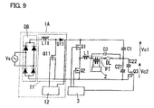
- FIG. 9 shows a configuration of a lighting apparatus of high intensity discharge lamp in accordance with the fourth embodiment.
- FIG. 10 shows timings of switching on and off of transistors Q 1 , Q 2 and Q 3 and waveforms of voltages V DL applied to a discharge lamp DL and V LC applied to an inductor L 1 and a capacitor C 3 .
- the lighting apparatus in the fourth embodiment further has a transistor Q 3 serially connected to the capacitor C 22 .
- the control circuit 3 switches on the transistor Q 3 while the discharge lamp DL has not been lighted, and switches off the transistor Q 3 while the discharge lamp DL has been lighted.
- the voltage V LC becomes a rectangular alternating voltage due to the voltage Vc 1 between the terminals of the capacitor C 1 and the voltage Vc 2 between the terminals of the parallel connection of the capacitors C 21 and C 22 .
- the motion of the lighting apparatus in the fourth embodiment becomes substantially the same as that in the second embodiment.
- the transistor Q 3 is switched off when the discharge lamp DL has been lighted, the voltage V LC becomes a rectangular alternating voltage due to the voltage Vc 1 between the terminals of the capacitor C 1 and the voltage Vc 21 between the terminals of the capacitor C 21 .
- the pulse heights in the positive and negative phases of the voltage V LC become equal to each other.
- the circuitry of the control circuit 3 can be designed substantially the same as that of the conventional circuitry of the control circuit.
- FIG. 11 shows a design specification of a lighting apparatus of high intensity discharge lamp in accordance with the fifth embodiment.
- the fifth embodiment relates to the design specification of the lighting apparatus.
- the lighting apparatus in the fifth embodiment has substantially the same circuitry as that in the second embodiment illustrated in FIG. 4 .
- the output voltage E from the DC power supply should be higher than the largest value of the input AC voltage for improving waveform distortion of the input current.
- the largest value of the input AC voltage is designated by a symbol Vsmax
- the inductance of the inductor L 11 is designated by a symbol L 11 .
- the value of current I on flowing in a loop of the inductor L 11 and the transistor Q 11 when the transistor Q 11 is switched on, the value I on is designated by the following equation (1).
- I on Vs max/ L 11 ⁇ t on (1)
- I off ( E ⁇ Vs max)/ L 11 ⁇ t off (2)
- Table 1 shows the spec of the lighting apparatus corresponding to effective values of input voltages.
- V Vc1 + Vc2 Vc1 (V) Vc2 (V) (Vc1/Vc2) 100 300–480 250–450 30–156 1.6–15 200 360–480 277 430–480
- the table 1 shows that the voltage E outputted from the DC power supply 1 A should be designed in a range from 360V to 480V, when the effective value of the commercial AC power source Vs is, for example 200V. Details of the table 1 are specifically described.
- Vsmax of the input AC voltage is calculated by the following equation (3) with regard to the variation of the commercial AC power source Vs about 10%. ⁇ square root over (2) ⁇ 200 ⁇ 1.1 ⁇ 310( V ) (3)
- the output voltage from the DC power supply 1 A is larger than the largest value of the input AC voltage.
- the larger the output voltage from the DC power supply 1 A the smoother the waveform distortion of the input current is reformed.
- the withstand voltage of the elements constituting the DC power supply 1 A becomes much higher corresponding to the increase of the output voltage from the DC power supply 1 A. It will cause the increase of stress burdening the elements and the upsizing of the elements.
- the upper limit of the voltage of the DC power supply 1 A is defined corresponding to multiplicity of voltage values of the DC power supply 1 A.
- the circuitry of the DC power supply 1 A such as the boosting chopper 11 is configured commonly with no relation to the effective value 100V, 200V or 277V of the AC power source.
- the largest value Vsmax of input AC voltage is calculated by the following equation (4). ⁇ square root over (2) ⁇ 277 ⁇ 1.1 ⁇ 430( V ) (4)
- the lower limit of the voltage of the DC power supply 1 A becomes 205V.
- the no-load voltage of the discharge lamp DL is 250V to 300V, so that the lower limit of the voltage of the DC power supply 1 A with respect to the effective value 100V should be 300V.
- the voltage V DL applied to the discharge lamp DL becomes equal to the voltage Vc 1 of the capacitor C 1 or the voltage Vc 2 of the parallel connection of the capacitors C 21 and C 22 . Since the lower limit of the no-load voltage applied to the discharge lamp DL while the discharge lamp DL has not been lighted is larger than about 250V to 300V, it is necessary to make the voltage Vc 1 of the capacitor C 1 be larger than 250V. Thus, the lower limit of the voltage Vc 1 is selected to be 250V. Hereupon, the largest value of the withstand voltage of the multipurpose electrolytic capacitor is 450V. Thus, the upper limit of the voltage Vc 1 is selected to be 450V.
- the lower limit of the voltage Vc 2 can be calculated by subtracting the value of the upper limit of the voltage Vc 1 from the value of the upper limit of the output voltage E from the DC power supply 1 A.
- the upper limit of the voltage Vc 2 can be calculated by subtracting the value of the lower limit of the voltage Vc 1 from the value of the upper limit of the output voltage E from the DC power supply 1 A.
- the tolerance of the values of capacitances of the capacitors is made allowance with about 20%.
- An upper limit and a lower limit of voltage ratio can be obtained by calculating the largest value and the smallest value of Vc 1 /Vc 2 .
- the upper limit if the voltage ratio becomes 15 ( 450V/30V).
- FIG. 11 shows the areas of the voltages Vc 1 and Vc 2 obtained in the table 1.
- the abscissa designates the value of the voltage Vc 1
- the ordinate designates the value of the voltage Vc 2 .
- a unionized area of areas designated by symbols A, B and C corresponds to the area suitable for the effective value 100V of the input AC voltage.
- a unionized area of the areas designated by the symbols A and B corresponds to the area suitable for the effective value 200V of the input AC voltage.
- the area designated by the symbol C corresponds to the area suitable for the effective value 277V of the input AC voltage.
- the discharge lamp DL could be extinguished while the discharge lamp DL has been lighted in rated voltage.
- the spec of the lighting apparatus is further selected in the area above the rated voltage V DL (N) illustrated by one dotted chain line in FIG. 11 .
- Vc 1 /Vc 2 the voltage ratio (Vc 1 /Vc 2 ) in the range from 1.6 to 15 so that the waveform distortion of the input current can be reformed when the effective value of the input AC voltage is in a region from 100V to 277V.
- the no-load voltage necessary for lighting the discharge lamp DL can be applied.
- FIG. 12 shows timings of switching on and off of transistors Q 1 and Q 23 , waveforms of currents I L1 flowing in an inductor L 1 and I DL flowing in a discharge lamp DL, and a waveform of a voltage V LC applied to an inductor L 1 and a capacitor C 3 in a lighting apparatus of high intensity discharge lamp in accordance with the sixth embodiment.
- the lighting apparatus in the sixth embodiment has substantially the same circuitry as that in the second embodiment illustrated in FIG. 4 .
- a switching frequency f 1 for switching on and off the transistor Q 1 is higher than a switching frequency f 2 for switching on and off the transistor Q 2 .
- the voltage Vc 1 in the alternating voltage V LC is defined by the voltage between the terminals of the capacitor C 1 and the voltage Vc 2 is defined by the voltage between the terminals of the parallel connection of the capacitors C 21 and C 22 .
- the pulse height Vc 1 of the voltage V LC in the term T 1 is higher than the pulse height Vc 2 in the term T 2 .
- the switching frequency f 2 of the transistor Q 2 switching on and off in the term T 2 is lower than the switching frequency f 1 of the transistor Q 1 switching on and off in the term T 1 .
- the absolute value of the current I L1 flowing in the inductor L 1 in the term T 2 becomes larger since the frequency f 2 reaches to the resonance frequency of the inductor L 1 and the capacitor C 3 .
- the pulse height of the current I L1 in the term T 2 is illustrated substantially the same as that in the term T 1 .
- Wave forms of the current I DL flowing in the discharge lamp DL in the positive phase become substantially the same as those in the negative phase, owing to a filter constituted by reactance component of the ignitor 2 and the capacitor C 3 . That is, the pulse height of the current I DL in the term T 1 becomes substantially the same as that in the term T 2 .
- the pulse height of the current I DL in the term T 1 can be made substantially the same as that in the term T 2 .
- FIG. 13 shows a configuration of a lighting apparatus of high intensity discharge lamp in accordance with the seventh embodiment.
- FIG. 14 shows timings of switching on and off of transistors Q 1 and Q 2 and waveform of current I L1 flowing in an inductor L 1 .
- the switching frequency f 1 of the transistor Q 1 in the term T 1 is integral multiple of the switching frequency f 2 of the transistor Q 2 in the term T 2 in the seventh embodiment.
- the control circuit 3 comprises a low frequency oscillator 31 , a high frequency oscillator 32 , a toggle flip-flop 300 , a NOT logic circuit 301 , two AND logic circuits 302 and 303 , and a driving circuit 33 .
- Output of the high frequency oscillator 32 is connected to an input terminal T of the toggle flip-flop 300 and an input terminal of the AND logic circuit 302 .
- An output terminal Q of the toggle flip-flop 300 is connected to an input terminal of the AND logic circuit 303 .
- Output of the low frequency oscillator 31 is connected to the other input terminal of the AND logic circuit 303 and the other input terminal of the AND logic circuit 302 via the NOT logic circuit 301 .
- Outputs of both AND logic circuit 302 and 303 are respectively connected to control terminals (gates) of the transistors Q 1 and Q 2 .
- the control circuit 3 when the high frequency oscillator 32 generates a signal having a frequency f 1 , another signal having a frequency f 2 which is a half of the frequency f 1 occurs in the output of the toggle flip-flop 300 . Subsequently, when the low frequency oscillator 31 generates a signal having a frequency of several hundreds Hz, the transistors Q 1 and Q 2 are alternately switched on and off in the low frequency of several hundreds Hz, and the transistor Q 1 is frequently switched on and off in the high frequency f 1 while the transistor Q 2 is switched off, and the transistor Q 2 is frequently switched on and off in a high frequency f 2 while the transistor Q 1 is switched off, as shown in FIG. 14 . It is possible to execute the power control of the discharge lamp DL by adding a circuit to the control circuit 3 for converting a duty ratio of the transistors Q 1 and Q 2 .
- the control circuit 3 can be configured by simple circuits.
- the discharge lamp DL has been lighted in a BCM (Boundary Current Mode) in negative positive phases of the voltage V DL applied to the discharge lamp DL. In the BCM, current continuously flows in the discharge lamp DL, but the discharge lamp starts to light when the current value becomes 0.
- BCM Battery Current Mode
- FIG. 15 shows a configuration of a lighting apparatus of high intensity discharge lamp in accordance with the eighth embodiment.
- FIG. 16 shows timings of switching on and off of transistors Q 3 and Q 4 , and waveforms of voltages V DL and V LC .
- the lighting apparatus in the eighth embodiment has a parallel connection of a capacitor C 11 and a series connection of a capacitor C 12 and a transistor (MOS-FET) Q 4 instead of the capacitor C 1 .
- the transistors Q 3 and Q 4 are alternately switched on and off by the control circuit 3 while the discharge lamp DL has not been lighted.
- Capacitances of the capacitors C 11 , C 12 , C 21 and C 22 are selected to be, for example, the same value.
- the transistor Q 3 is switched on and the transistor Q 4 is switched off in a term TS 1 .
- the transistor Q 3 is switched off and the transistor Q 4 is switched on in a term TS 2 having the same time period as the term TS 1 .
- the capacitors C 11 , C 21 and C 22 are connected, so that the voltage Vc 1 becomes larger than the voltage Vc 2 .
- the motion of the lighting apparatus becomes substantially the same as that in the second embodiment.
- the capacitors C 11 , C 12 and C 21 are connected, so that the voltage Vc 1 becomes smaller than the voltage Vc 2 .
- the voltage having a wave form that the pulse height Vc 2 of the voltage V LC in the negative phase is higher than the pulse height Vc 1 in the positive phase in the term TS 2 is applied to the discharge lamp DL, as shown in FIG. 16 .
- the pulse height Vc 1 of the voltage V LC in the term T 1 of the term TS 1 becomes the same as the pulse height Vc 2 in the term T 2 of the term TS 2
- the pulse height Vc 2 in the term T 2 of the term TS 1 becomes the same as the pulse height Vc 1 in the term T 1 of the term TS 2 .
- the ratio of the total capacitance of the capacitors C 11 and C 12 with respect to the total capacitance of the capacitances C 21 and C 22 is alternately varied in the terms TS 1 and TS 2 , so that the stresses applied to the terminals of the discharge lamp DL become substantially even. It is advantageous with respect to the life of the discharge lamp DL.
- the switching timing between the mode of Vc 1 >Vc 2 and the mode of VC 1 ⁇ Vc 2 is not restricted by the above-mentioned terms TS 1 and TS 2 .
- a number of lighting of the discharge lamp DL is memorized. It is possible to switch the mode of Vc 1 >Vc 2 to the other mode of Vc 1 ⁇ Vc 2 when the number of lighting is an even number, and the mode of Vc 1 ⁇ Vc 2 is switched to the other mode of Vc 1 >Vc 2 when the number of lighting is an odd number, and vice versa.
- FIG. 17 shows a configuration of a lighting apparatus of high intensity discharge lamp in accordance with the ninth embodiment.
- FIG. 18 shows timings of switching on and off of a switch S 12 , and waveforms of voltages V DL and V LC .
- the lighting apparatus in the ninth embodiment further comprises a voltage sensing circuit 4 for sensing the voltage applied to the discharge lamp DL.
- the control circuit 12 is configured to switch the output of the DC power supply 1 A corresponding to the voltage sensed by the voltage sensing circuit 4 .
- a series connection of a capacitor C 41 and two resistors R 41 and R 42 is connected between the connection point of the inductor L 1 and the capacitor C 3 and the ground.
- a series connection of a diode D 41 and a capacitor C 42 is further connected in parallel with the resistor R 42 .
- a voltage generated in the capacitor C 42 is taken into the control circuit 12 as a sensed voltage.
- an output voltage (Vc 1 +Vc 2 ) from the DC power supply 1 A is inputted to a negative input terminal of an operational amplifier 121 through a resistor R 122 , which is a divisional voltage of resistors R 120 and R 121 .
- a resistor R 123 is connected between the negative input terminal and an output terminal of the operational amplifier 121 , so that error component of the voltage of output from the DC power supply 1 A is amplified with a gain R 123 /R 122 of the values of the resistors R 122 and R 123 .
- Alternative of a reference voltage Vref and the sensed voltage is inputted to a positive input terminal of the operational amplifier 121 through the switch S 12 .
- An output signal from a high frequency oscillator 122 is inputted to a positive input terminal of a comparator 123 .
- the output terminal of the operational amplifier 121 is connected to a negative input terminal of the comparator 123 , so that a value of the input voltage to the negative input terminal of the comparator 123 is compared with a pulse height of a high frequency waveform of the output signal from the high frequency oscillator 122 .
- a driving circuit 124 switched on and off the transistor Q 11 corresponding to the result of comparison.
- the switch S 12 is turned to a contact S 122 while the discharge lamp DL has not been lighted, so that the voltages Vc 1 and Vc 2 are set to be, for example, 300V and 150V.
- the voltage V DL has waveforms that the high frequency and high voltage pulses are superimposed on low frequency rectangular alternating voltage component V LC .
- the switch S 12 is turned to a contact S 121 corresponding to a judgment of a lighting discriminating circuit (not shown in the figure), so that the input to the positive input terminal of the operational amplifier 121 is switched to a value corresponding to the voltage between the terminals of the discharge lamp DL. Since the voltage between the terminals of the discharge lamp DL at the start of lighting is very small and gradually increases, the voltages Vc 1 and Vc 2 are gradually increased corresponding to the increase of the sensed voltage.
- the switch S 12 is turned to the terminal S 122 again, and the voltages Vc 1 and Vc 2 are respectively switched to 300V and 150V.
- the value of DC voltages applied to the discharge lamp DL in the term TS 121 just after the discharge lamp DL has been lighted can be reduces as smaller as possible at which the discharge lamp DL may not be extinct.
- efficiency of the boosting chopper 11 while the discharge lamp has been lighted can be increased.
- FIG. 19 shows a configuration of a lighting apparatus of high intensity discharge lamp in accordance with the tenth embodiment.
- FIGS. 20A and 20B respectively show waveforms of voltages Vref, Vc 1 +Vc 2 and V LC when the lighting apparatus is connected to different AC power sources having different effective voltages.
- the lighting apparatus in the tenth embodiment has a voltage sensing circuit 5 for sensing the voltage of the output of the DC power supply 1 A instead of the voltage sensing circuit 4 .
- the control circuit 12 is configured to switch the output of the DC power supply 1 A corresponding to the voltage sensed by the voltage sensing circuit 5 .
- the voltage sensing circuit 5 is configured by a series connection of two resistors R 51 and R 52 connected between a terminal of the diode bridge DB and the ground, a capacitor C 5 connected in parallel with the resistor R 52 , and a comparator 51 .
- the voltage between output terminals of the diode bridge DB is sensed as a voltage Vc 5 between the terminals of the capacitor C 5 .
- the voltage Vc 5 is inputted to a negative terminal of the comparator 51 , and compared with a reference voltage Vref inputted to a positive input terminal of the comparator 51 .
- the result of comparison of the comparator 51 is used for switching the switch S 12 in the control circuit 12 .
- the control circuit 12 in the tenth embodiment is substantially the same as that in the ninth embodiment except that reference voltages Vref 1 and Vref 2 (Vref 1 >Vref 2 ) are applied to the terminals S 121 and S 122 of the switch S 12 .
- the switch S 12 is turned to the terminal S 121 .
- the voltage Vc 5 becomes lower than the reference voltage Vref, as shown in FIG. 20B .
- the switch S 12 is turned to the terminal S 122 .
- the output voltage from the DC power supply 1 A in a range from 300V to 360V.
- the output voltage from the DC power supply 1 A is varied corresponding to the effective value of the commercial AC power source Vs, it is possible to restrict unnecessary increase of the output voltage from the DC power supply 1 A, even when the input value of the commercial AC power source Vs is not so high.
- the boosting chopper 11 can be used effective.
- the lighting apparatus in the tenth embodiment can be modified as illustrated in FIGS. 21 , 22 and 23 .
- a DC power supply 1 B in FIG. 21 comprises only the diode bridge DB and the inductor L 11 .
- the transistor Q 2 in the inverter of half-bridge circuitry serves as a function of the transistor Q 11 in the boosting chopper 11 illustrated in FIG. 19 .
- a DC power supply 1 C in FIG. 22 comprises the diode bridge DB, a series connection of capacitors C 110 and C 111 connected between the diodes and the inductor L 11 .
- the transistors Q 1 and Q 2 in the inverter serve as a function of the transistor Q 11 in the boosting chopper 11 .
- a DC power supply 1 D in FIG. 23 comprises the diode bridge DB, a boosting chopper 11 configured by two transistors QI 1 and Q 12 , diodes D 11 and D 12 and the inductor L 11 , and a control circuit 12 A for switching on and off the transistors Q 11 and Q 12 .
- the DC power supply 1 A can output the DC voltage in a predetermined region.
- the characteristics for starting up the discharge lamp DL can be improved by setting the voltages Vc 1 and Vc 2 uneven owing to the capacitances of the capacitors C 1 and C 2 .
- FIG. 24 shows timings of switching on and off of transistors Q 1 and Q 2 , and waveforms of voltages Vc 1 , Vc 2 and V DL in a lighting apparatus in accordance with the eleventh embodiment.
- the eleventh embodiment relates to driving method of the lighting apparatus.
- the circuitry of the lighting apparatus is, for example, substantially the same as that in the first embodiment illustrated in FIG. 1 .
- the control circuit 3 switches on and off the transistors Q 1 and Q 2 in a manner so that a frequency of rectangular alternating voltage component of a voltage V DL applied to the discharge lamp DL in a predetermined term T 3 after the start up of lighting of the discharge lamp DL becomes lower than that after passing the term T 3 .
- the frequency of the rectangular alternating voltage component is set to be lower than the normal frequency in the predetermined term T 3 after starting up of the lighting of the discharge lamp DL.
- the frequency of the rectangular alternating voltage component in the term T 3 is several tens Hz, and the normal frequency thereof after passing the term T 3 is several hundreds Hz.
- FIG. 25 shows a configuration of a lighting apparatus of high intensity discharge lamp in accordance with the twelfth embodiment.
- FIG. 26 shows timings of switching on and off of transistors Q 1 and Q 2 , and waveforms of voltages Vc 1 , Vc 2 and V DL .
- the frequency of rectangular alternating voltage component of the voltage V DL applied to the discharge lamp DL in the term T 3 is the inverse number of a time necessary for roundly varying the voltage between terminals of at least one of the capacitors C 1 and C 2 from the higher voltage Vc 1 to the lower voltage Vc 2 , roundly.
- the lighting apparatus has a voltage sensing circuit 4 similar to that in the ninth embodiment, and a voltage sensing circuit 6 configured by resistors R 61 and R 62 for sensing voltages of terminals of the capacitors C 1 and C 2 , further to the circuitry illustrated in FIG. 1 .
- the control circuit 3 is configured by low frequency oscillators 30 and 31 , a high frequency oscillator 32 , a driving circuit 33 , a flip-flop 310 , a plurality of comparators 311 to 315 and a logic circuit 320 .
- the control circuit 3 switches on and off the transistors Q 1 and Q 2 corresponding to the voltages sensed by the voltage sensing circuits 4 and 6 , as shown in FIG. 26 .
- the low frequency of the rectangular alternating voltage component is set to be, for example, several tens Hz.
- High frequency and high voltage pulses Vp due to the ignitor 2 are superimposed on the rectangular alternating voltage component, so that the voltage V DL applied to the discharge lamp DL has the waveform as illustrated in FIG. 26 .
- the transistors Q 1 and Q 2 are switched on and off in a manner so that the frequency of the rectangular alternating voltage component of the voltage V DL in the term T 3 after starting up of lighting of the discharge lamp DL becomes lower than that after passing the term T 3 .
- the frequency of the rectangular alternating voltage component in the term T 3 is defined by the voltages Vc 1 and Vc 2 of the capacitors C 1 and C 2 .
- FIG. 27 shows a configuration of a lighting apparatus of high intensity discharge lamp in accordance with the thirteenth embodiment.
- FIG. 28 shows timings of switching on and off of transistors Q 1 and Q 2 , and waveforms of voltages Vc 1 , Vc 2 and V DL .
- the frequency of rectangular alternating voltage component of the voltage V DL applied to the discharge lamp DL in the term T 3 is the inverse number of a time necessary for roundly varying the voltage between terminals of at least one of the capacitors C 1 and C 2 from a voltage Vc 1 max to a voltage E-Vc 1 max.
- the voltage Vc 1 max is the largest value of the voltage Vc 1 applicable to the capacitances C 1 and C 2 .
- the voltage E is the output voltage from the DC power supply 1 A.
- the lighting apparatus has a voltage sensing circuit 4 and a voltage sensing circuit 6 similar to those in the eleventh embodiment, and a voltage sensing circuit 7 configured by resistors R 71 and R 72 for sensing the output voltage E of the DC power supply 1 A, further to the circuitry illustrated in FIG. 1 .
- the control circuit 3 is configured by low frequency oscillators 30 and 31 , a high frequency oscillator 32 , a driving circuit 33 , a flip-flop 310 , a plurality of comparators 311 to 315 , an operational amplifier 316 and a logic circuit 320 .
- the control circuit 3 switches on and off the transistors Q 1 and Q 2 corresponding to the voltages sensed by the voltage sensing circuits 4 , 6 and 7 , as shown in FIG. 28 .
- the low frequency of the rectangular alternating voltage component is set to be, for example, several tens Hz.
- High frequency and high voltage pulses Vp due to the ignitor 2 are superimposed on the rectangular alternating voltage component, so that the voltage V DL applied to the discharge lamp DL has the waveform as illustrated in FIG. 28 .
- the transistors Q 1 and Q 2 are switched on and off in a manner so that the frequency of the rectangular alternating voltage component of the voltage V DL in the term T 3 after starting up of lighting of the discharge lamp DL becomes lower than that after passing the term T 3 .
- the frequency of the rectangular alternating voltage component in the term T 3 is defined by the largest voltage applicable to the capacitors C 1 and C 2 .
- the output voltage E of the DC power supply 1 A is 450V and the largest voltage applicable to the capacitors C 1 and C 2 is 420V.
- voltages Vr 1 and Vr 2 are respectively selected to be the values of Vc 1 max and E-Vc 1 max.
- the discharge of the discharge lamp DL can be stabilized owing to reduce the number of inversion of negative phase and positive phase of the voltages V DL in the term T 3 just after start up of lighting.
- FIG. 29 shows a configuration of a lighting apparatus of high intensity discharge lamp in accordance with the fourteenth embodiment.
- FIG. 30 shows timings of switching on and off of transistors Q 1 and Q 2 , and waveforms of voltages Vc 1 , Vc 2 and V DL .
- the frequency of rectangular alternating voltage component of the voltage V DL applied to the discharge lamp DL in the term T 3 is the inverse number of a time necessary for roundly varying the voltage between terminals of at least one of the capacitors C 1 and C 2 from a predetermined voltage Vc to a voltage E-Vc.
- the voltage E is the output voltage from the DC power supply 1 A.
- the lighting apparatus has a voltage sensing circuit 4 and a voltage sensing circuit 7 similar to those in the thirteenth embodiment, further to the circuitry illustrated in FIG. 1 .
- the control circuit 3 is configured by low frequency oscillators 30 and 31 , a high frequency oscillator 32 , a driving circuit 33 , a flip-flop 310 , a plurality of comparators 311 to 315 , an operational amplifier 316 and a logic circuit 320 .
- the control circuit 3 switches on and off the transistors Q 1 and Q 2 corresponding to the voltages sensed by the voltage sensing circuits 4 and 7 , as shown in FIG. 30 .
- the low frequency of the rectangular alternating voltage component is set to be, for example, several tens Hz.
- High frequency and high voltage pulses Vp due to the ignitor 2 are superimposed on the rectangular alternating voltage component, so that the voltage V DL applied to the discharge lamp DL has the waveform as illustrated in FIG. 30 .
- the transistors Q 1 and Q 2 are switched on and off in a manner so that the frequency of the rectangular alternating voltage component of the voltage V DL in the term T 3 after starting up of lighting of the discharge lamp DL becomes lower than that after passing the term T 3 .
- the frequency of the rectangular alternating voltage component in the term T 3 is defined by the voltage Vc of the discharge lamp DL just after passing the term T 3 .
- the value of the voltage Vc is not sensed after passing the term T 3 , but known experientially.
- the discharge lamp DL is started up the lighting at the output voltage E of the DC power supply 1 A is 450V, and the voltage Vc of the discharge lamp DL just after the starting up of the lighting is experientially known as about 50V.
- voltages Vr 1 and Vr 2 are respectively selected to the values of Vc and E-Vc.
- T 3 the lower the voltage of the discharge lamp DL becomes.
- FIG. 31 shows a configuration of a lighting apparatus of high intensity discharge lamp in accordance with the fifteenth embodiment.
- FIG. 32 shows timings of switching on and off of transistors Q 1 and Q 2 , and waveforms of voltages Vc 1 , Vc 2 and V DL .
- the lighting apparatus has a voltage sensing circuit 4 and a voltage sensing circuit 8 for sensing voltages between the terminals of the capacitors C 1 and C 2 , further to the circuitry illustrated in FIG. 1 .
- the control circuit 3 switches on and off the transistors Q 1 and Q 2 utilizing the voltage of the discharge lamp DL and the voltage of at least one of the capacitors C 1 and C 2 .
- the ignitor 2 is omitted the illustration.
- a sensing result of the voltage of the discharge lamp DL is used for switching on and off the transistors Q 1 and Q 2 .
- a sensing result of the voltage of at least one of the capacitors C 1 and C 2 is used.
- FIG. 33 shows a configuration of a lighting apparatus of high intensity discharge lamp in accordance with the sixteenth embodiment.
- the lighting apparatus in the sixteenth embodiment illustrated in FIG. 33 comprises a voltage sensing circuit 6 for sensing the voltage of both terminals of the capacitor C 2 instead of the voltage sensing circuit 8 .
- a sensing result of the voltage of the discharge lamp DL is used for switching on and off the transistors Q 1 and Q 2 .
- a sensing result of the voltage of the capacitor C 2 is used in the rest half period of the rectangular alternating voltage component of the voltage V DL .
- the ignitor 2 is omitted the illustration.
- the control circuit 3 since the control circuit 3 uses only the voltage of the capacitor C 2 for switching on and off the transistor Q 2 in the half period of the rectangular alternating voltage component of the voltage V DL applied to the discharge lamp DL, the voltage sensing circuit 6 can directly sense the voltage of the capacitor C 2 from the reference voltage. Thus, the voltage sensing circuit 6 can be simplified.
- the capacitance of the capacitor C 2 is made larger than that of the capacitor C 1 for applying the voltage V DL having different pulse heights in the negative and positive phases to the discharge lamp DL corresponding to the frequencies of the rectangular alternating voltage component, it is possible to reduce the power loss due to resistors for sensing the voltage in the sensing of the voltage Vc 2 by voltage division of the resistors.
- FIG. 34 shows a configuration of a lighting apparatus of high intensity discharge lamp in accordance with the seventeenth embodiment.
- FIG. 35 shows timings of switching on and off of transistors Q 1 and Q 2 , and waveforms of voltages Vc 1 , Vc 2 and V DL .
- FIG. 36 shows a fundamental configuration of the lighting apparatus in the seventeenth embodiment.
- FIG. 37 shows a reason for modifying the configuration from the fundamental configuration illustrated in FIG. 36 to the configuration illustrated in FIG. 34 .
- FIG. 38 shows timings of switching on and off of transistors Q 1 and Q 2 , and waveforms of currents I 1 , I 2 and I DL .
- FIG. 39 shows a characteristic of gain-frequency of low-pass filters of the lighting apparatus in the seventeenth embodiment.
- the lighting apparatus in the seventeenth embodiment has essentially the same configuration as that in the first embodiment.
- the control circuit 3 (not illustrated in FIG. 34 ) not only switches on and off the transistors Q 1 and Q 2 as shown in FIG. 35 , but also controls current flowing in the inductor L 1 .
- the inductor L 1 and the capacitor C 3 configures a first low-pass filter and an inductor L 2 and a capacitor C 4 configures a second low-pass filter, so that the gain of the double low-pass filters in the negative and positive phases of a current I DL flowing in the discharge lamp DL become substantially the same.
- the switching frequency of the transistor Q 1 naturally becomes higher than the switching frequency of the transistor Q 2 , as shown in FIG. 38 .
- the gain (Vout/Vin) of the low-pass filter configured by the inductor L 1 and the capacitor C 3 varies corresponding to the difference of the switching frequencies of the transistors q 1 and Q 2 .
- the content of ripple contained in the current I DL flowing in the discharge lamp DL in the term T 1 will be different from that in the term T 2 due to switching on and off of the transistors Q 1 and Q 2 .
- the capacitor C 4 in order to make the content of ripple in the current I DL in the negative be the same as that in the positive phase, the capacitor C 4 is connected in parallel with a series connection of the inductor L 1 , the ignitor 2 and the discharge lamp DL, and the inductor L 2 is connected between the connection point of the capacitors Q 1 and Q 2 and the inductor L 1 . Since the capacitor C 4 and the inductor L 2 configures a filter, so that the lighting apparatus in the seventeenth embodiment has double low-pass filters configured by the capacitor C 3 and the inductor L 1 , and the capacitor C 4 and the inductor L 2 . Thus, the low-pass filter of the lighting apparatus in the seventeenth embodiment has the characteristic of gain-frequency shown in FIG. 39 .
- the switching frequency of the transistor Q 1 is different from that of the transistor Q 2 , it is possible to obtain substantially the same gains owing to the switching operation of the transistors Q 1 and Q 2 , so that the contents of ripple in the current I DL flowing in the discharge lamp DL in the negative and positive phases become substantially the same.
- FIG. 40 shows a configuration of a lighting apparatus of high intensity discharge lamp in accordance with the eighteenth embodiment.
- the lighting apparatus in the eighteenth embodiment illustrated in FIG. 40 varies a value of inductance of the inductor L 1 corresponding to the negative and positive phases of a current flowing in the inductor L 1 .
- the lighting apparatus comprises a parallel connection of series connection of the inductor L 1 and a diode D 3 and a series connection of the inductor L 2 and a diode D 4 , which is connected between the connection point of the transistors Q 1 and Q 2 and the ignitor 2 .
- the diodes D 3 and D 4 are respectively connected in the opposite directions.
- the inductor L 2 and the capacitor C 3 configure a low-pass filter.
- the inductor L 1 and the capacitor C 3 configure a low-pass filter.
- FIG. 41 shows a configuration of a lighting apparatus of high intensity discharge lamp in accordance with the nineteenth embodiment.
- the lighting apparatus in the nineteenth embodiment varies the capacitance of the capacitor C 3 connected in parallel with the discharge lamp DL (see, for example, FIG. 1 ) corresponding to the negative and positive phases of the current flowing in the inductor L 1 .
- a parallel connection of a capacitor C 5 1 ns a diode D 5 is connected between a capacitor C 3 ′ and the ignitor 2 .
- the inductor L 1 and the capacitors C 3 ′ and C 5 configure a low-pass filter.
- the inductor L 1 and the capacitor C 3 ′ configure a low-pass filter.
- FIG. 42 shows timings of switching on and off of transistors Q 1 and Q 2 , and waveforms of currents I 1 , I 2 and I DL in accordance with the twentieth embodiment.
- the twentieth embodiment relates to the control method of the lighting apparatus, so that the illustration of the circuitry of the lighting apparatus is omitted.
- the lighting apparatus in the twentieth embodiment controls the currents I 1 and I 1 ′ flowing in the capacitor C 1 having the higher voltage Vc 1 in DCM (Discontinuous Current Mode), and controls the currents I 2 and I 2 ′ flowing in the capacitor C 2 in the BCM.
- the DCM is a control by which the current is discontinuously flown.
- the switching frequency of the transistor Q 1 is decreased to be substantially the same as the switching frequency of the transistor Q 2 .
- the width of on period of the transistor Q 1 is made narrower, so that the current I 1 and I 1 ′ flowing in the capacitor C 1 is controlled in the DCM.
- the switching frequencies of the transistors Q 1 and q 2 can be made substantially the same.
- FIG. 43 shows timings of switching on and off of transistors Q 1 and Q 2 , and waveforms of currents I 1 , I 2 and I DL in accordance with the twenty-first embodiment.
- the twenty-first embodiment relates to the control method of the lighting apparatus, so that the illustration of the circuitry of the lighting apparatus is omitted.
- the lighting apparatus in the twenty-first embodiment controls the currents I 2 and I 2 ′ flowing in the capacitor C 2 having the lower voltage Vc 2 in CCM (Continuous Current Mode), and controls the currents I 1 and I 1 ′ flowing in the capacitor C 1 in the BCM.
- the CCM is a control by which the current is continuously flown.
- the switching frequency of the transistor Q 2 is increased to be substantially the same as the switching frequency of the transistor Q 1 .
- the width of on period of the transistor Q 2 is made wider, so that the current I 2 and I 2 ′ flowing in the capacitor C 2 is controlled in the CCM.
- the switching frequencies of the transistors Q 1 and q 2 can be made substantially the same.
- FIG. 44 shows timings of switching on and off of transistors Q 1 and Q 2 , and waveforms of currents I 1 , I 2 and I DL in accordance with the twenty-second embodiment.
- the twenty-second embodiment relates to the control method of the lighting apparatus, so that the illustration of the circuitry of the lighting apparatus is omitted.
- the lighting apparatus in the twenty-second embodiment controls the currents I 1 and I 1 ′ flowing in the capacitor C 1 having the higher voltage Vc 2 in the DCM, and controls the currents I 2 and I 2 ′ flowing in the capacitor C 2 in the CCM.
- the switching frequency of the transistor Q 1 is decreased and the switching frequency of the transistor Q 2 is increased so as to make the switching frequencies of the transistors Q 1 and Q 2 be substantially the same.
- the width of on period of the transistor Q 1 is made narrower, so that the current I 1 and I 1 ′ flowing in the capacitor C 1 is controlled in the DCM.
- the width of on period of the transistor Q 2 is made wider, so that the current I 2 and I 2 ′ flowing in the capacitor C 2 is controlled in the CCM.
- the switching frequencies of the transistors Q 1 and q 2 can be made substantially the same.
- FIG. 45 shows a configuration of a lighting apparatus of high intensity discharge lamp in accordance with the twenty-third embodiment.
- FIG. 46 shows timings of switching on and off of transistors Q 1 , Q 2 and Q 3 , and waveforms of voltages Vc 1 , Vc 2 and V DL .
- the lighting apparatus in the twenty-third embodiment illustrated in FIG. 45 comprises a compensator for compensating the voltages Vc 1 and Vc 2 of the capacitors to predetermined voltages further to the configuration of the circuitry illustrated in FIG. 1 .
- the compensator is configured by a series connection of a transistor Q 3 and a diode D 6 which is connected in parallel with the series connection of the capacitors C 1 and C 2 , and an inductor L 3 connected between the connection point of the capacitors C 1 and C 2 and a connection point of the transistor Q 3 and the diode D 6 .
- the diode D 6 interdicts currents from the capacitors C 1 and C 2 .
- the transistors Q 2 and Q 3 are always switched off, and the transistors Q 1 is frequently switched on and off in a high frequency by a control circuit not illustrated in FIG. 45 while the discharge lamp DL has not been lighted.
- the voltage V DL having the waveform that the high frequency and high voltage alternating voltages owing to the ignitor 2 are superimposed on the voltage Vc 1 between the terminals of the capacitor C 1 is applied to the discharge lamp DL.
- the lighting apparatus of high intensity discharge lamp in accordance with the present invention can prevent the increase of the stresses or upsizing of the elements can be prevented, and can make the transition from glow discharge to arc discharge after lighting the discharge lamp smoothly.
Abstract
Description
I on =Vsmax/L 11 ·t on (1)
I off=(E−Vsmax)/L 11 ·t off (2)
| TABLE 1 | ||||
| INPUT VOLTAGE (V) | VOLTAGE RATIO | |||
| (EFFECTIVE VALUE) | E (V) = Vc1 + Vc2 | Vc1 (V) | Vc2 (V) | (Vc1/Vc2) |
| 100 | 300–480 | 250–450 | 30–156 | 1.6–15 |
| 200 | 360–480 | |||
| 277 | 430–480 | |||
√{square root over (2)}×200×1.1≈310(V) (3)
√{square root over (2)}×277×1.1≈430(V) (4)
Claims (25)
Applications Claiming Priority (3)
| Application Number | Priority Date | Filing Date | Title |
|---|---|---|---|
| JP2003-098014 | 2003-04-01 | ||
| JP2003098014A JP4348984B2 (en) | 2003-04-01 | 2003-04-01 | High pressure discharge lamp lighting device |
| PCT/JP2004/004745 WO2004091263A1 (en) | 2003-04-01 | 2004-03-31 | Lighting apparatus of high intensity discharge lamp |
Publications (2)
| Publication Number | Publication Date |
|---|---|
| US20050269963A1 US20050269963A1 (en) | 2005-12-08 |
| US7129650B2 true US7129650B2 (en) | 2006-10-31 |
Family
ID=33156660
Family Applications (1)
| Application Number | Title | Priority Date | Filing Date |
|---|---|---|---|
| US10/526,446 Expired - Fee Related US7129650B2 (en) | 2003-04-01 | 2004-03-31 | Lighting apparatus for high intensity discharge lamp |
Country Status (4)
| Country | Link |
|---|---|
| US (1) | US7129650B2 (en) |
| EP (1) | EP1609337A1 (en) |
| JP (1) | JP4348984B2 (en) |
| WO (1) | WO2004091263A1 (en) |
Cited By (6)
| Publication number | Priority date | Publication date | Assignee | Title |
|---|---|---|---|---|
| US20060261755A1 (en) * | 2005-04-11 | 2006-11-23 | Nucon Gbr | Circuit and method for the operation of miniature high pressure short-arc lamps using alternating current |
| US20070170873A1 (en) * | 2004-03-26 | 2007-07-26 | Matsushita Electric Works, Ltd. | High-pressure discharge lamp lighting device and lighting fixture |
| US20090315470A1 (en) * | 2006-08-23 | 2009-12-24 | Panasonic Electric Works Co., Ltd. | High-pressure discharge lamp lighting device and lighting fixture using the same |
| US20100060180A1 (en) * | 2007-04-24 | 2010-03-11 | Osram Gesellschaft Mit Beschraenkter Haftung | Circuit arrangement for igniting and operating a discharge lamp |
| US20110006695A1 (en) * | 2008-02-25 | 2011-01-13 | Kaestle Herbert | Device and Method for Generating an Ignition Voltage for a Lamp |
| US20110316434A1 (en) * | 2009-02-13 | 2011-12-29 | Koninklijke Philips Electronics N.V. | Electro magnetic ballast for a gas discharge lamp |
Families Citing this family (10)
| Publication number | Priority date | Publication date | Assignee | Title |
|---|---|---|---|---|
| KR101046924B1 (en) * | 2004-05-11 | 2011-07-06 | 삼성전자주식회사 | Back light assembly and display device having same |
| JP2006228479A (en) * | 2005-02-15 | 2006-08-31 | Matsushita Electric Works Ltd | High pressure discharge lamp lighting device, luminaire and lighting system |
| JP4876463B2 (en) * | 2005-07-14 | 2012-02-15 | パナソニック電工株式会社 | Discharge lamp lighting device, lighting fixture, and lighting system |
| CN1960594A (en) * | 2005-10-31 | 2007-05-09 | 皇家飞利浦电子股份有限公司 | Starting device for gaseous discharging lamp |
| DE102006028821A1 (en) * | 2006-06-21 | 2007-12-27 | Patent-Treuhand-Gesellschaft für elektrische Glühlampen mbH | Apparatus and method for operating a high pressure discharge lamp |
| US7432664B2 (en) * | 2006-09-29 | 2008-10-07 | Osram Sylvania Inc. | Circuit for powering a high intensity discharge lamp |
| JP5491716B2 (en) * | 2008-10-07 | 2014-05-14 | 株式会社アイ・ライティング・システム | Discharge lamp lighting device |
| JP2010129235A (en) * | 2008-11-25 | 2010-06-10 | Panasonic Electric Works Co Ltd | Discharge lamp lighting device and illumination device using the same, and projector |
| US9910095B2 (en) * | 2012-12-13 | 2018-03-06 | John Manford Wade | Voltage measurement for multiple cell battery pack |
| JP5491810B2 (en) * | 2009-09-25 | 2014-05-14 | パナソニック株式会社 | Discharge lamp lighting device and lighting fixture |
Citations (11)
| Publication number | Priority date | Publication date | Assignee | Title |
|---|---|---|---|---|
| US4904903A (en) * | 1988-04-05 | 1990-02-27 | Innovative Controls, Inc. | Ballast for high intensity discharge lamps |
| US5010279A (en) * | 1985-08-26 | 1991-04-23 | Lathom Michael S | Switched capacitive ballasts for discharge lamps |
| US5739644A (en) * | 1994-03-11 | 1998-04-14 | Patent-Treuhand-Gesellschaft F. Elektrische Gluehlampen Mbh | Discharge lamp typically a sodium high-pressure discharge lamp, from an a-c power network |
| US5875107A (en) * | 1996-12-05 | 1999-02-23 | Mitsubishi Denki Kabushiki Kaisha | Inverter apparatus |
| CA2255512A1 (en) | 1997-12-12 | 1999-06-12 | Da Feng Weng | Ballast for discharge lamp |
| JP2948600B2 (en) | 1989-06-27 | 1999-09-13 | 松下電工株式会社 | Inverter device |
| US6018220A (en) * | 1997-07-21 | 2000-01-25 | General Electric Company | Gas discharge lamp ballast circuit with a non-electrolytic smoothing capacitor for rectified current |
| US6020691A (en) | 1999-04-30 | 2000-02-01 | Matsushita Electric Works R & D Laboratory, Inc. | Driving circuit for high intensity discharge lamp electronic ballast |
| US6075715A (en) * | 1997-03-26 | 2000-06-13 | Matsushita Electric Works, Ltd. | Power source device |
| US6144172A (en) | 1999-05-14 | 2000-11-07 | Matsushita Electric Works R&D Laboratory, Inc. | Method and driving circuit for HID lamp electronic ballast |
| US6459215B1 (en) * | 2000-08-11 | 2002-10-01 | General Electric Company | Integral lamp |
-
2003
- 2003-04-01 JP JP2003098014A patent/JP4348984B2/en not_active Expired - Fee Related
-
2004
- 2004-03-31 EP EP04724850A patent/EP1609337A1/en not_active Ceased
- 2004-03-31 WO PCT/JP2004/004745 patent/WO2004091263A1/en active Application Filing
- 2004-03-31 US US10/526,446 patent/US7129650B2/en not_active Expired - Fee Related
Patent Citations (11)
| Publication number | Priority date | Publication date | Assignee | Title |
|---|---|---|---|---|
| US5010279A (en) * | 1985-08-26 | 1991-04-23 | Lathom Michael S | Switched capacitive ballasts for discharge lamps |
| US4904903A (en) * | 1988-04-05 | 1990-02-27 | Innovative Controls, Inc. | Ballast for high intensity discharge lamps |
| JP2948600B2 (en) | 1989-06-27 | 1999-09-13 | 松下電工株式会社 | Inverter device |
| US5739644A (en) * | 1994-03-11 | 1998-04-14 | Patent-Treuhand-Gesellschaft F. Elektrische Gluehlampen Mbh | Discharge lamp typically a sodium high-pressure discharge lamp, from an a-c power network |
| US5875107A (en) * | 1996-12-05 | 1999-02-23 | Mitsubishi Denki Kabushiki Kaisha | Inverter apparatus |
| US6075715A (en) * | 1997-03-26 | 2000-06-13 | Matsushita Electric Works, Ltd. | Power source device |
| US6018220A (en) * | 1997-07-21 | 2000-01-25 | General Electric Company | Gas discharge lamp ballast circuit with a non-electrolytic smoothing capacitor for rectified current |
| CA2255512A1 (en) | 1997-12-12 | 1999-06-12 | Da Feng Weng | Ballast for discharge lamp |
| US6020691A (en) | 1999-04-30 | 2000-02-01 | Matsushita Electric Works R & D Laboratory, Inc. | Driving circuit for high intensity discharge lamp electronic ballast |
| US6144172A (en) | 1999-05-14 | 2000-11-07 | Matsushita Electric Works R&D Laboratory, Inc. | Method and driving circuit for HID lamp electronic ballast |
| US6459215B1 (en) * | 2000-08-11 | 2002-10-01 | General Electric Company | Integral lamp |
Non-Patent Citations (1)
| Title |
|---|
| English Language Abstract of JP 3-03029, Aug. 2, 1991. |
Cited By (10)
| Publication number | Priority date | Publication date | Assignee | Title |
|---|---|---|---|---|
| US20070170873A1 (en) * | 2004-03-26 | 2007-07-26 | Matsushita Electric Works, Ltd. | High-pressure discharge lamp lighting device and lighting fixture |
| US7615937B2 (en) | 2004-03-26 | 2009-11-10 | Panasonic Electric Works Co., Ltd. | High-pressure discharge lamp lighting device and lighting fixture |
| US20060261755A1 (en) * | 2005-04-11 | 2006-11-23 | Nucon Gbr | Circuit and method for the operation of miniature high pressure short-arc lamps using alternating current |
| US7586270B2 (en) * | 2005-04-11 | 2009-09-08 | Nucon Gbr | Circuit and method for the operation of miniature high pressure short-arc lamps using alternating current |
| US20090315470A1 (en) * | 2006-08-23 | 2009-12-24 | Panasonic Electric Works Co., Ltd. | High-pressure discharge lamp lighting device and lighting fixture using the same |
| US8395327B2 (en) | 2006-08-23 | 2013-03-12 | Panasonic Corporation | High-pressure discharge lamp lighting device and lighting fixture using the same |
| US20100060180A1 (en) * | 2007-04-24 | 2010-03-11 | Osram Gesellschaft Mit Beschraenkter Haftung | Circuit arrangement for igniting and operating a discharge lamp |
| US20110006695A1 (en) * | 2008-02-25 | 2011-01-13 | Kaestle Herbert | Device and Method for Generating an Ignition Voltage for a Lamp |
| US20110316434A1 (en) * | 2009-02-13 | 2011-12-29 | Koninklijke Philips Electronics N.V. | Electro magnetic ballast for a gas discharge lamp |
| US8395333B2 (en) * | 2009-02-13 | 2013-03-12 | Koninklijke Philips Electronics N.V. | Electro magnetic ballast for a gas discharge lamp |
Also Published As
| Publication number | Publication date |
|---|---|
| JP2004303689A (en) | 2004-10-28 |
| JP4348984B2 (en) | 2009-10-21 |
| EP1609337A1 (en) | 2005-12-28 |
| US20050269963A1 (en) | 2005-12-08 |
| WO2004091263A1 (en) | 2004-10-21 |
Similar Documents
| Publication | Publication Date | Title |
|---|---|---|
| RU2540418C2 (en) | Brightness control of excitation circuit of light-emitting diodes | |
| US7129650B2 (en) | Lighting apparatus for high intensity discharge lamp | |
| US9065350B2 (en) | Resonant converter control based on a voltage difference | |
| JP4253341B2 (en) | Discharge lamp lighting control device | |
| JP6702010B2 (en) | Switching power supply | |
| KR20010098937A (en) | Light emitting diode driving apparatus | |
| US8264161B2 (en) | Lighting apparatus for high-voltage discharge lamp | |
| US9119274B2 (en) | Resonant converter control | |
| JP6895502B2 (en) | Dimming circuit and dimming control method | |
| CN108365766B (en) | LLC quasi-resonance switch power supply | |
| KR20090105229A (en) | Parallel operation of interleaved switching converter circuit | |
| Qiu et al. | A novel bipolar series Ripple compensation method for single-stage high-power LED driver | |
| CN217508578U (en) | Power supply controller | |
| JP4649728B2 (en) | Power supply device and discharge lamp lighting device | |
| CN116937938A (en) | Control method for power factor correction and power supply controller | |
| JP2004303688A (en) | Discharge lamp lighting device | |
| JP3888062B2 (en) | Discharge lamp lighting device | |
| JP2000012260A (en) | Discharge lamp lighting device | |
| JPH06310288A (en) | Discharge lamp lighting device | |
| JPH09289771A (en) | Switching power supply unit | |
| EP1773104A1 (en) | Discharge lamp lighting device and illumination apparatus | |
| JPH11285269A (en) | Power supply unit | |
| JPH113794A (en) | Lighting device for illumination | |
| JPH1116688A (en) | Power source device | |
| JPH08328670A (en) | Power controller |
Legal Events
| Date | Code | Title | Description |
|---|---|---|---|
| AS | Assignment |
Owner name: MATSUSHITA ELECTRIC WORKS, LTD., JAPAN Free format text: ASSIGNMENT OF ASSIGNORS INTEREST;ASSIGNORS:KOMATSU, NAOKI;MISHIMA, MASANORI;MAEHARA, MINORU;AND OTHERS;REEL/FRAME:016957/0291 Effective date: 20050221 |
|
| FEPP | Fee payment procedure |
Free format text: PAYOR NUMBER ASSIGNED (ORIGINAL EVENT CODE: ASPN); ENTITY STATUS OF PATENT OWNER: LARGE ENTITY |
|
| AS | Assignment |
Owner name: PANASONIC ELECTRIC WORKS CO., LTD., JAPAN Free format text: CHANGE OF NAME;ASSIGNOR:MATSUSHITA ELECTRIC WORKS, LTD.;REEL/FRAME:022191/0478 Effective date: 20081001 Owner name: PANASONIC ELECTRIC WORKS CO., LTD.,JAPAN Free format text: CHANGE OF NAME;ASSIGNOR:MATSUSHITA ELECTRIC WORKS, LTD.;REEL/FRAME:022191/0478 Effective date: 20081001 |
|
| FPAY | Fee payment |
Year of fee payment: 4 |
|
| FEPP | Fee payment procedure |
Free format text: PAYER NUMBER DE-ASSIGNED (ORIGINAL EVENT CODE: RMPN); ENTITY STATUS OF PATENT OWNER: LARGE ENTITY Free format text: PAYOR NUMBER ASSIGNED (ORIGINAL EVENT CODE: ASPN); ENTITY STATUS OF PATENT OWNER: LARGE ENTITY |
|
| FPAY | Fee payment |
Year of fee payment: 8 |
|
| FEPP | Fee payment procedure |
Free format text: MAINTENANCE FEE REMINDER MAILED (ORIGINAL EVENT CODE: REM.) |
|
| LAPS | Lapse for failure to pay maintenance fees |
Free format text: PATENT EXPIRED FOR FAILURE TO PAY MAINTENANCE FEES (ORIGINAL EVENT CODE: EXP.); ENTITY STATUS OF PATENT OWNER: LARGE ENTITY |
|
| STCH | Information on status: patent discontinuation |
Free format text: PATENT EXPIRED DUE TO NONPAYMENT OF MAINTENANCE FEES UNDER 37 CFR 1.362 |
|
| FP | Lapsed due to failure to pay maintenance fee |
Effective date: 20181031 |