US7126397B1 - Pulse width modulation carrier frequency technique - Google Patents
Pulse width modulation carrier frequency technique Download PDFInfo
- Publication number
- US7126397B1 US7126397B1 US11/026,713 US2671304A US7126397B1 US 7126397 B1 US7126397 B1 US 7126397B1 US 2671304 A US2671304 A US 2671304A US 7126397 B1 US7126397 B1 US 7126397B1
- Authority
- US
- United States
- Prior art keywords
- circuit
- duty cycle
- frequency
- pwm signal
- pwm
- Prior art date
- Legal status (The legal status is an assumption and is not a legal conclusion. Google has not performed a legal analysis and makes no representation as to the accuracy of the status listed.)
- Active, expires
Links
- 238000000034 method Methods 0.000 title claims abstract description 28
- 238000005070 sampling Methods 0.000 claims description 31
- 239000003990 capacitor Substances 0.000 claims description 25
- 238000006243 chemical reaction Methods 0.000 claims description 22
- 238000000605 extraction Methods 0.000 claims description 11
- 239000000284 extract Substances 0.000 claims description 4
- 238000010586 diagram Methods 0.000 description 9
- 238000004519 manufacturing process Methods 0.000 description 4
- 230000008569 process Effects 0.000 description 4
- 239000004065 semiconductor Substances 0.000 description 4
- 238000012986 modification Methods 0.000 description 3
- 230000004048 modification Effects 0.000 description 3
- 238000012935 Averaging Methods 0.000 description 2
- 230000007274 generation of a signal involved in cell-cell signaling Effects 0.000 description 2
- 229910021420 polycrystalline silicon Inorganic materials 0.000 description 2
- 229920005591 polysilicon Polymers 0.000 description 2
- 230000009467 reduction Effects 0.000 description 2
- 230000000903 blocking effect Effects 0.000 description 1
- 238000007796 conventional method Methods 0.000 description 1
- 239000013078 crystal Substances 0.000 description 1
- 238000001914 filtration Methods 0.000 description 1
Images


Classifications
-
- H—ELECTRICITY
- H03—ELECTRONIC CIRCUITRY
- H03K—PULSE TECHNIQUE
- H03K7/00—Modulating pulses with a continuously-variable modulating signal
- H03K7/08—Duration or width modulation ; Duty cycle modulation
Definitions
- Embodiments of the present invention generally pertain to the field of electronic circuits. More particularly, embodiments of the present invention are related to techniques for controlling the carrier frequency of a pulse width modulated signal.
- FIG. 1A illustrates a conventional circuit 100 for generating a PWM signal from a ramp voltage reference and an input signal.
- the widths of respective pulses in the PWM signal are modulated based on the input signal.
- the PWM signal has a carrier frequency “f ref ” that is the same frequency as the ramp voltage reference.
- the duty cycle of each period of the PWM signal depends upon the relative magnitudes of the ramped reference signal and the input signal.
- the duty cycle of the PWM signal contains information about the magnitude of the input signal.
- FIG. 1B illustrates a conventional circuit 150 for generating a ramped reference voltage, which may be used to create the PWM signal having the same frequency “f ref ” as the ramped reference voltage signal.
- the ramped voltage circuit 150 functions by charging the capacitor C ref with the bias current I bias until the capacitor C ref is at the reference voltage V Dc — ref . During this period, the output voltage ramps up. When the output voltage reaches the reference voltage, the capacitor C ref rapidly discharges to create the saw-tooth waveform of the output ramped reference voltage.
- the present invention provides a method and circuit that generate a PWM signal at a desired carrier frequency.
- Embodiments of the present invention generate a low carrier frequency PWM signal.
- Embodiments of the present invention do not require a large on-chip capacitor for generation of a low carrier frequency PWM signal.
- Embodiments of the present invention provide a low carrier frequency PWM signal generation circuit that is compatible with and can be fabricated economically with existing semiconductor fabrication techniques.
- a method and circuit for generating a PWM signal is disclosed.
- a temporary PWM signal is generated at a first frequency.
- the temporary PWM signal includes analog duty cycle information adapted for the first frequency. At least a portion of the analog duty cycle information is converted to digital duty cycle information adapted for a second frequency.
- a final PWM signal having a carrier frequency of the second frequency is generated from the digital duty cycle information.
- the circuit includes temporary pulse-width modulated (PWM) generation logic that generates a temporary pulse-width modulated (PWM) signal comprising analog duty cycle information.
- PWM pulse-width modulated
- the circuit further includes conversion logic that converts at least a portion of the analog duty cycle information to digital duty cycle information adapted for a second frequency.
- the circuit also has final PWM generation logic that generates a final PWM signal from the digital duty cycle information adapted for the second frequency.
- the final PWM has a carrier frequency of the second frequency.
- FIG. 1A is a diagram of a conventional circuit for generating a pulse width modulated signal.
- FIG. 1B is a diagram of a conventional circuit for generating a ramped voltage reference.
- FIG. 2 is a block diagram of a circuit for generating a PWM signal at a desired carrier frequency, in accordance with an embodiment of the present invention.
- FIG. 3A duty cycle conversion logic depicts in accordance with an embodiment of the present invention.
- FIG. 3B is a block diagram of duty cycle conversion logic in which the duty cycle extraction logic first extracts temporary digital duty cycle samples from pulses of a temporary PWM signal in accordance with an embodiment of the present invention.
- FIG. 4 is a diagram illustrating down sampling a PWM signal, in accordance with an embodiment of the present invention.
- FIG. 5 is diagram illustrating converting duty cycle information that is adapted for one frequency such that it is adapted for another frequency, in accordance with an embodiment of the present invention.
- FIG. 6 is flowchart illustrating steps of a process of generating a PWM signal, in accordance with an embodiment of the present invention.
- FIG. 7A illustrates an exemplary circuit for generating a master clock, in accordance with one embodiment of the present invention.
- FIG. 7B illustrates an exemplary circuit for generating a ramped voltage, in accordance with one embodiment of the present invention.
- FIG. 7C illustrates an exemplary circuit for generating a bias current for the master clock circuit of FIG. 7A .
- FIG. 7D illustrates an exemplary circuit for generating a bias current for the ramp voltage reference circuit of FIG. 7B , in accordance with one embodiment of the present invention.
- a PWM signal it is desirable for a PWM signal to have a low carrier frequency. Moreover, it is desirable for the carrier frequency of the PWM signal to be programmable.
- conventional techniques for generating a low-frequency PWM signal typically require a very large capacitor. Unfortunately, a large capacitor requires considerable die area. While the capacitor could be located externally, this solution undesirably requires an additional pin.
- Embodiments of the present invention provide methods and circuits that are able to generate a low carrier frequency PWM generator. Embodiments of the present invention provide for programming the carrier frequency of the PWM output signal. Embodiments of the present invention do not require a large capacitor to generate a low carrier frequency PWM signal. Embodiments of the present invention are compatible with and can be fabricated economically with existing semiconductor fabrication techniques.
- the carrier frequency of the PWM signal will be equal to the frequency of the ramped voltage signal, in this circuit.
- the bias current I bias cannot be made small enough or the reference voltage V DC-ref large enough to create a low frequency ramped reference voltage.
- using a very low bias current could lead to circuit stability problems.
- accurately generating a very low bias current can be difficult. Therefore, it can be difficult to generate a low carrier frequency PWM from the ramped reference voltage by using a very low bias current.
- one technique to achieve a low carrier frequency PWM signal is to use a very large reference capacitor (e.g., C ref ).
- C ref very large reference capacitor
- using a large capacitor is undesirable.
- One reason a large capacitor is undesirable is the large die area required for a large capacitor.
- the reference capacitor could be located externally; however, this solution undesirably requires an additional pin.
- FIG. 2 is a block diagram of a PWM circuit 200 that is able to generate a low carrier frequency pulse width modulator, in accordance with an embodiment of the present invention. Further, the circuit 200 is programmable to allow the carrier frequency f c of the output PWM signal PWM out to be programmed.
- the PWM circuit 200 receives a master clock (M clk ), which is used for various elements in circuit 200 .
- the master clock signal may be generated by an external crystal oscillator, an external clock source, a phase locked loop (PLL), etc. It will be appreciated that the master clock signal may be generated on-chip as a part of circuit 200 .
- the clock divide 270 receives the master clock M clk and divides it for the use of various components. Thus, the various components use clock signals that have a known relationship to the master clock M clk .
- the clock divide 270 also optionally receives a clock program signal “Pgm” that indicates how the master clock M clk should be divided. This allows the carrier frequency f c of the output PWM signal PWM out to be programmed to a desired frequency.
- the ramp voltage generator 220 inputs a clock M clk /R having a known relationship to the master clock M clk and generates a ramped voltage signal V ramp having the frequency of the clock M clk /R.
- the frequency of the ramped voltage signal V ramp has a known relationship to the frequency of the master clock M clk .
- the ratio of the frequency of the master clock M clk to the frequency of ramped voltage signal V ramp is a known and controlled value. In some embodiments, the ratio is a power of two, although the present invention is not so limited.
- the comparator 230 generates a temporary PWM signal PWM temp from its inputs of the ramped voltage signal V ramp and an input signal of interest.
- the carrier frequency of the temporary PWM signal PWM temp is at the frequency of the ramped voltage signal V ramp . Therefore, the temporary PWM signal has a carrier frequency that is a known ratio to the frequency of the master clock M clk .
- the temporary PWM signal has a duty cycle that comprises information about the input signal.
- the duty cycle may be a function of the magnitude of the input signal.
- the temporary PWM signal comprises analog duty cycle information in that the width of its pulses may comprise information about the magnitude input signal. However, is not required that the analog duty cycle information related to the magnitude of the input signal.
- the duty cycle of the temporary PWM signal PWM temp is not constant over time. Rather, the duty cycle may be different for different cycles of the temporary PWM signal PWM temp .
- the input signal may be any signal of interest. Further, the input signal may be processed by, for example, filtering, rectifying, peak-detecting, etc.
- the temporary PWM signal PWM temp comprises analog duty cycle information adapted to the frequency of the ramped voltage signal M clk /R.
- a duty cycle adapted to a given frequency can be any value from 0–100%. This allows the full pulse width to be used to store information. However, it is not required that the full pulse width be used to store information for a signal to have its duty cycle adapted to a given frequency.
- the conversion logic 235 generates digital duty cycle information that is adapted to the frequency f c of the final PWM signal PWM out .
- the conversion logic 235 inputs the temporary PWM signal PWM temp , a clock having the desired carrier frequency f c , the master clock M clk , and the clock M clk /R and outputs digital duty cycle information.
- the PWM generation logic 256 receives the digital duty cycle information and a clock whose frequency is “f c *R” and outputs the final PWM signal.
- the PWM generation logic 256 may comprise a D/A converter.
- the conversion logic 235 has down-sampling logic 240 and duty cycle extraction logic 255 .
- the down sampling logic 240 may process the temporary PWM signal PWM temp prior to the duty cycle extraction logic 235 or afterwards.
- FIG. 3A depicts an embodiment of the duty cycle conversion logic 235 .
- the down sampling logic 240 inputs the temporary PWM signal PWM temp and a sampling clock.
- the sampling clock has the frequency f c of the desired carrier frequency of the output PWM signal.
- the down-sampling logic 240 generates a down-sampled PWM signal PWM down at a down-sampled frequency from the temporary PWM signal PWM temp .
- the down-sampled frequency is the desired carrier frequency f c of the final PWM signal.
- the down sampling may be implemented by logic that passes portions of the temporary PWM signal, while blocking other portions.
- the conversion logic 235 also has duty cycle extraction logic 255 .
- the duty cycle extraction logic 255 inputs the down-sampled signal PWM down from down sampling 240 .
- the duty cycle extraction logic 255 also receives the master clock M clk and the clock M clk /R that was input to the ramp voltage generator 220 .
- the duty cycle extraction logic 255 outputs digital duty cycle information.
- the duty cycle converter 235 has an A/D converter (e.g., up counter 257 ) coupled to the down-sampling logic 240 .
- the A/D converter converts the analog duty cycle information of the down-sampled PWM signal PWM down into digital data.
- the counter 257 uses the master clock M clk to count to determine the width of each pulse (whose width is determined by the clock M clk /R) in the down-sampled PWM signal. It is not required that the A/D be implemented with a counter.
- FIG. 4 provides an illustration of down sampling a PWM signal with exemplary frequencies and duty cycles, in accordance with an embodiment of the present invention.
- a temporary PWM signal 310 with a carrier frequency of 20 kHz is sampled by a 10 Hz sampling clock 320 to produce down-sampled PWM signal 330 .
- the high time of sampling clock 320 can be equal to one period or multiple periods of temporary PWM signal 310 .
- the carrier frequency of the down-sampled PWM signal 330 is equal to the frequency of the sampling clock.
- the width of the pulses in the down-sampled PWM signal 330 are the same as the corresponding pulses in the temporary PWM signal 310 .
- the duty cycle of the down-sampled PWM signal 330 should be adjusted to correctly convey the information.
- the duty cycle should be adapted to the down sampled frequency.
- the widths of the pulses in the down-sampled PWM signal 330 should be made wider to account for the reduction in the carrier frequency from 20 KHz to 10 Hz.
- the down-sampled PWM signal 330 can be averaged prior to making its resultant period wider to take into account the frequency reduction due to the down-sampling.
- the averaging can be implemented by, for example, an A/D counter.
- FIG. 3B is a block diagram of an embodiment of the duty cycle conversion logic 235 in which the duty cycle extraction logic 255 first extracts temporary digital duty cycle samples from pulses of the temporary PWM signal PWM TEMP . This may result in more samples than are required for the frequency of the final PWM signal. At this point the temporary digital duty cycle information is adapted for the frequency of the ramped voltage reference signal. Then the down-sampling logic 240 processes this digital duty cycle information to adapt it for the carrier frequency of the output PWM signal. For example, the down-sampling logic 240 may average the digital duty cycle information to effectively down-sample the digital duty cycle information. However, the down sampling is not limited to averaging. There may be greater latency with this embodiment that the embodiment that first down-samples and then extracts the digital duty cycle information from the down-sampled signal.
- the PWM generation logic 256 outputs the final PWM signal PWM out signal based on the digital duty cycle information adapted for the down-sampled frequency. Furthermore, the PWM generation logic 256 access a clock running at the carrier frequency f c of the PWM signal times the ratio (R) of the master clock frequency M clk to the frequency of the clock into the ramp voltage reference M clk /R. In other words, this clock has a frequency of “f c *R”, where f c is the carrier frequency of the final PWM signal and “R” is the factor by which the master clock M clk was divided to generate the clock for the ramp voltage generator 220 .
- the PWM generation logic 256 may be implemented by a digital-to-analog converter (D/A) that receives the digital duty cycle information from the duty cycle conversion logic 235 .
- the D/A can be implemented by counting down for the number of counts in the digital duty cycle information. For example, in the embodiment in FIG. 3A a down counter 258 is used. So long as the count is non-zero, the D/A outputs a “high” signal for the final PWM signal PWM out . When the count hits zero, the D/A outputs a “low” signal for the final PWM signal.
- FIG. 5 is diagram illustrating of adapting the duty cycle of the temporary PWM signal 330 for the frequency of the final PWM signal, in accordance with an embodiment of the present invention.
- the final PWM signal is generated with the widths of its pulses adapted such that the duty cycle is the correct percentage of the period of the final PWM signal.
- the waveforms in FIG. 5 are exemplary.
- the duty cycle of the depicted pulse of the temporary PWM 330 would be 75% if the period were “R/M clk ”.
- “R/M clk ” is the period of the temporary PWM signal output by the comparator 230 .
- the period of the down-sampled PWM signal 330 is “1/f c ”, where f c is the carrier frequency of the final PWM signal.
- the duty cycle of the temporary PWM signal 330 is not adapted to the carrier frequency f c .
- the master clock M clk is used to convert analog duty cycle information of the temporary PWM signal 330 to digital data.
- the master clock M clk is used to count the width of the pulse in the exemplary PWM signal 330 .
- an up-counter is incremented for each clock cycle of the master clock.
- the master clock were divided by 32 to create the ramped reference voltage (e.g., “R” is 32), then there would be 24 counts given the exemplary 75% duty cycle.
- This count is input to the PWM generation logic ( 256 , FIG. 2 ) along with the clock with frequency of “f c *R” to generate the final PWM signal.
- the PWM generation logic 256 counts down for a number of pulses specified by the count parameter. In this embodiment, the latency may be as low as one clock cycle of the master clock M clk .
- the carrier frequency f c of the final PWM signal is programmable.
- docks input to the duty cycle conversion logic 235 and the PWM generation logic 256 are adjusted.
- a value e.g., “pgm” may be sent to the clock divide circuit 270 .
- the clock divide circuit adjusts the frequency of the clock with frequency “f c *R” that is input to the PWM generation logic 256 , and the sampling clock with frequency f c that is input to the duty cycle conversion logic 235 . It is not required that the value “R” be adjusted.
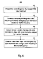
- FIG. 6 is a flowchart illustrating steps of a process for generating a PWM signal, in accordance with an embodiment of the present invention.
- Step 610 is an optional step of programming the carrier frequency of an output PWM signal.
- the programming may include programming a clock rate used in down-sampling a temporary PWM signal in step 620 .
- a clock rate used in generating the final PWM signal from the digital duty cycle information may be programmed in step 640 .
- Step 620 is generating a temporary PWM signal at a first frequency.
- the temporary PWM signal has analog duty cycle information adapted for the first frequency.
- Step 620 may include generating a fixed ramp reference voltage at a first frequency.
- the first frequency has a pre-determined relationship to a master clock frequency. For example, the pre-determined relationship is a ratio of the first frequency to the master clock frequency.
- Step 630 is converting at least a portion of the analog duty cycle information to digital duty cycle information adapted for a second frequency.
- the second frequency is the carrier frequency of the output PWM signal.
- Step 630 may comprise down sampling the temporary PWM signal to produce a down-sampled PWM signal at the second frequency. Further, step 630 may comprise extracting the digital duty cycle information from pulses of the down-sampled PWM signal.
- step 630 may comprise extracting temporary digital duty cycle information from pulses of the temporary PWM signal.
- the temporary digital duty cycle information is adapted for the first frequency.
- Step 630 further includes converting the temporary digital duty cycle information to the digital duty cycle information adapted for the second frequency, in this alternative sequence.
- Step 640 is generating a final PWM signal from the digital duty cycle information.
- Step 640 may include converting the digital duty cycle information to widths of pulses of the final PWM.
- the final PWM has a carrier frequency of the second frequency.
- FIG. 7A illustrates an exemplary circuit 700 for generating a master clock M clk , in accordance with one embodiment of the present invention.
- the circuit 700 of FIG. 7A comprises a comparator with inputs of voltage reference (V DC — ref — clk ) and a bias current (I clk ) and a capacitor (C clk ). The output of the comparator controls the switch coupled to the bias current I clk .
- FIG. 7B illustrates an exemplary circuit 720 for generating a ramped voltage, in accordance with one embodiment of the present invention.
- the frequency of the ramped voltage V ramo is controlled by the clock input M clk /R.
- the clock M clk /R may be derived from the clock signal M clk generated by circuit 700 of FIG. 7A .
- the master clock M clk may be divided down by a series of flip-flops.
- the circuit 720 of FIG. 7B comprises a bias current (I ramp ) coupled to a capacitor (C ramp ) via a switch.
- the circuit receives a clock signal M clk /R, which is used to control the switch between the bias current I ramp and the capacitor.
- the output V ramp is taken from the capacitor C ramp .
- the peak voltage value of V ramp is defined as V ramp — max .
- V ramp — max is V dd /2, where V dd is depicted in FIG. 7D and included in Equation 5 herein.
- FIG. 7C illustrates an exemplary circuit 760 for generating a bias current I clk for the master clock circuit 700 of FIG. 7A , in accordance with one embodiment of the present invention.
- FIG. 7D illustrates an exemplary circuit 780 for generating a bias current I ramp for the ramp voltage reference circuit 720 of FIG. 7B , in accordance with one embodiment of the present invention.
- an operational amplifier has its output coupled to the gate of a current mirror, which supplies the bias current (I clk ) for the master clock circuit 700 .
- the inverting input of the op-amp is coupled to a reference voltage (V BG ) and the non-inverting input is coupled to a resistor (R 1 ).
- the ratio of the transistors in the current mirror is 1:d.
- an operational amplifier has its output coupled to the gate of a current mirror, which supplies the bias current (I ramp ) for the ramp voltage reference circuit 720 .
- the inverting input of the op-amp is coupled to a reference voltage (V dd/2 ) and the non-inverting input is coupled to a resistor (R 2 ).
- the ratio of the transistors in the current mirror is 1:e.
- Equation 2 the period (t clk ) of the master clock M clk will be given by Equation 2 and Equation 3.
- t clk C clk *V clk /I clk Eq. 2
- C clk *V clk /I clk C clk *V BG /[( d ) ( V BG /R 1 )] Eq. 3
- Equation 4 the period (t ramp ) of the ramp voltage reference V ramp will be given by Equation 4 and Equation 5.
- t ramp C ramp *V rmap — max /I ramp Eq. 4
- C ramp *V rmap — max /I ramp [C ramp *V dd /2]/[( e ) ( V dd /2)/ R 2 )] Eq. 5
- Equation 6 follows from Equations 4 and 5.
- C ramp *R 2 /e ( C clk *R 1 /d )* R Eq. 6
- the result is component matching of capacitors and resistors, which allows accurate control of V ramp — max of the ramp voltage reference and control of relationship of the carrier frequency of the signals used in the circuit.
- the capacitors may be double polysilicon capacitors and the resistors may be high resistive polysilicon resistors.
- embodiments of the present invention provide a method and circuit for a PWM signal generator.
- Embodiments of the present invention provide for programming the carrier frequency of the PWM output signal.
- Embodiments of the present invention do not require a large capacitor to generate a low carrier frequency PWM signal.
- Embodiments of the present invention are compatible with and can be fabricated economically with existing semiconductor fabrication techniques.
Abstract
A PWM method and circuit. A temporary PWM signal is generated at a first frequency. The temporary PWM signal includes analog duty cycle information adapted for the first frequency. At least a portion of the analog duty cycle information is converted to digital duty cycle information adapted for a second frequency. A final PWM signal having a carrier frequency of the second frequency is generated from the digital duty cycle information.
Description
Embodiments of the present invention generally pertain to the field of electronic circuits. More particularly, embodiments of the present invention are related to techniques for controlling the carrier frequency of a pulse width modulated signal.
Many integrated circuit applications require a pulse width modulated (PWM) signal. FIG. 1A illustrates a conventional circuit 100 for generating a PWM signal from a ramp voltage reference and an input signal. The widths of respective pulses in the PWM signal are modulated based on the input signal. The PWM signal has a carrier frequency “fref” that is the same frequency as the ramp voltage reference. The duty cycle of each period of the PWM signal depends upon the relative magnitudes of the ramped reference signal and the input signal. Thus, the duty cycle of the PWM signal contains information about the magnitude of the input signal.
The present invention provides a method and circuit that generate a PWM signal at a desired carrier frequency. Embodiments of the present invention generate a low carrier frequency PWM signal. Embodiments of the present invention do not require a large on-chip capacitor for generation of a low carrier frequency PWM signal. Embodiments of the present invention provide a low carrier frequency PWM signal generation circuit that is compatible with and can be fabricated economically with existing semiconductor fabrication techniques.
A method and circuit for generating a PWM signal is disclosed. In one embodiment, a temporary PWM signal is generated at a first frequency. The temporary PWM signal includes analog duty cycle information adapted for the first frequency. At least a portion of the analog duty cycle information is converted to digital duty cycle information adapted for a second frequency. A final PWM signal having a carrier frequency of the second frequency is generated from the digital duty cycle information.
Another embodiment in accordance with the present invention is a circuit for generating a pulse-width modulated signal. The circuit includes temporary pulse-width modulated (PWM) generation logic that generates a temporary pulse-width modulated (PWM) signal comprising analog duty cycle information. The circuit further includes conversion logic that converts at least a portion of the analog duty cycle information to digital duty cycle information adapted for a second frequency. The circuit also has final PWM generation logic that generates a final PWM signal from the digital duty cycle information adapted for the second frequency. The final PWM has a carrier frequency of the second frequency.
These and other advantages of the present invention will no doubt become obvious to those of ordinary skill in the art after having read the following detailed description of the preferred embodiments, which are illustrated in the various drawing figures.
The accompanying drawings, which are incorporated in and form a part of this specification, illustrate embodiments of the invention and, together with the description, serve to explain the principles of the invention:
Reference will now be made in detail to the preferred embodiments of the invention, pulse width modulated signal generation, examples of which are illustrated in the accompanying drawings. While the invention will be described in conjunction with the preferred embodiments, it will be understood that they are not intended to limit the invention to these embodiments. On the contrary, the invention is intended to cover alternatives, modifications and equivalents, which may be included within the spirit and scope of the invention as defined by the appended claims. Furthermore, in the following detailed description of the present invention, numerous specific details are set forth in order to provide a thorough understanding of the present invention. However, it will be obvious to one of ordinary skill in the art that the present invention may be practiced without these specific details. In other instances, well-known methods, procedures, components, and circuits have not been described in detail as not to unnecessarily obscure aspects of the present invention.
In some applications, it is desirable for a PWM signal to have a low carrier frequency. Moreover, it is desirable for the carrier frequency of the PWM signal to be programmable. However, conventional techniques for generating a low-frequency PWM signal typically require a very large capacitor. Unfortunately, a large capacitor requires considerable die area. While the capacitor could be located externally, this solution undesirably requires an additional pin.
Thus, a need exists for a low carrier frequency PWM signal generator. A further need exists for programming the carrier frequency of the PWM output signal. A still further need exists for low carrier frequency PWM generation that does not require a large capacitor. A further need exists for a low carrier frequency PWM circuit that is compatible with and can be fabricated economically with existing semiconductor fabrication techniques.
Embodiments of the present invention provide methods and circuits that are able to generate a low carrier frequency PWM generator. Embodiments of the present invention provide for programming the carrier frequency of the PWM output signal. Embodiments of the present invention do not require a large capacitor to generate a low carrier frequency PWM signal. Embodiments of the present invention are compatible with and can be fabricated economically with existing semiconductor fabrication techniques.
Referring again to FIG. 1A , the carrier frequency of the PWM signal will be equal to the frequency of the ramped voltage signal, in this circuit. Referring again to FIG. 1B , the frequency of the ramped voltage signal depends on the rate of charging the capacitor as shown in Equation 1.
f=I bias/(C ref *V DC-ref)Equation 1
f=I bias/(C ref *V DC-ref)
For practical reasons, the bias current Ibias cannot be made small enough or the reference voltage VDC-ref large enough to create a low frequency ramped reference voltage. For example, using a very low bias current could lead to circuit stability problems. Moreover, accurately generating a very low bias current can be difficult. Therefore, it can be difficult to generate a low carrier frequency PWM from the ramped reference voltage by using a very low bias current.
Thus, one technique to achieve a low carrier frequency PWM signal is to use a very large reference capacitor (e.g., Cref). However, using a large capacitor is undesirable. One reason a large capacitor is undesirable is the large die area required for a large capacitor. Alternatively, the reference capacitor could be located externally; however, this solution undesirably requires an additional pin.
The PWM circuit 200 receives a master clock (Mclk), which is used for various elements in circuit 200. The master clock signal may be generated by an external crystal oscillator, an external clock source, a phase locked loop (PLL), etc. It will be appreciated that the master clock signal may be generated on-chip as a part of circuit 200.
The clock divide 270 receives the master clock Mclk and divides it for the use of various components. Thus, the various components use clock signals that have a known relationship to the master clock Mclk. The clock divide 270 also optionally receives a clock program signal “Pgm” that indicates how the master clock Mclk should be divided. This allows the carrier frequency fc of the output PWM signal PWMout to be programmed to a desired frequency.
The ramp voltage generator 220 inputs a clock Mclk/R having a known relationship to the master clock Mclk and generates a ramped voltage signal Vramp having the frequency of the clock Mclk/R. Thus, the frequency of the ramped voltage signal Vramp has a known relationship to the frequency of the master clock Mclk. For example, the ratio of the frequency of the master clock Mclk to the frequency of ramped voltage signal Vramp is a known and controlled value. In some embodiments, the ratio is a power of two, although the present invention is not so limited.
The comparator 230 generates a temporary PWM signal PWMtemp from its inputs of the ramped voltage signal Vramp and an input signal of interest. Thus, the carrier frequency of the temporary PWM signal PWMtemp is at the frequency of the ramped voltage signal Vramp. Therefore, the temporary PWM signal has a carrier frequency that is a known ratio to the frequency of the master clock Mclk. Furthermore, the temporary PWM signal has a duty cycle that comprises information about the input signal. For example, the duty cycle may be a function of the magnitude of the input signal. Thus, the temporary PWM signal comprises analog duty cycle information in that the width of its pulses may comprise information about the magnitude input signal. However, is not required that the analog duty cycle information related to the magnitude of the input signal.
It will be appreciated that the duty cycle of the temporary PWM signal PWMtemp is not constant over time. Rather, the duty cycle may be different for different cycles of the temporary PWM signal PWMtemp. The input signal may be any signal of interest. Further, the input signal may be processed by, for example, filtering, rectifying, peak-detecting, etc.
The temporary PWM signal PWMtemp comprises analog duty cycle information adapted to the frequency of the ramped voltage signal Mclk/R. In one embodiment, a duty cycle adapted to a given frequency can be any value from 0–100%. This allows the full pulse width to be used to store information. However, it is not required that the full pulse width be used to store information for a signal to have its duty cycle adapted to a given frequency. The conversion logic 235 generates digital duty cycle information that is adapted to the frequency fc of the final PWM signal PWMout. The conversion logic 235 inputs the temporary PWM signal PWMtemp, a clock having the desired carrier frequency fc, the master clock Mclk, and the clock Mclk/R and outputs digital duty cycle information. The PWM generation logic 256 receives the digital duty cycle information and a clock whose frequency is “fc*R” and outputs the final PWM signal. The PWM generation logic 256 may comprise a D/A converter.
The conversion logic 235 has down-sampling logic 240 and duty cycle extraction logic 255. The down sampling logic 240 may process the temporary PWM signal PWMtemp prior to the duty cycle extraction logic 235 or afterwards. FIG. 3A depicts an embodiment of the duty cycle conversion logic 235. The down sampling logic 240 inputs the temporary PWM signal PWMtemp and a sampling clock. The sampling clock has the frequency fc of the desired carrier frequency of the output PWM signal. Thus, the down-sampling logic 240 generates a down-sampled PWM signal PWMdown at a down-sampled frequency from the temporary PWM signal PWMtemp. The down-sampled frequency is the desired carrier frequency fc of the final PWM signal. The down sampling may be implemented by logic that passes portions of the temporary PWM signal, while blocking other portions.
The conversion logic 235 also has duty cycle extraction logic 255. The duty cycle extraction logic 255 inputs the down-sampled signal PWMdown from down sampling 240. The duty cycle extraction logic 255 also receives the master clock Mclk and the clock Mclk/R that was input to the ramp voltage generator 220. The duty cycle extraction logic 255 outputs digital duty cycle information.
In this embodiment, the duty cycle converter 235 has an A/D converter (e.g., up counter 257) coupled to the down-sampling logic 240. The A/D converter converts the analog duty cycle information of the down-sampled PWM signal PWMdown into digital data. For example, the counter 257 uses the master clock Mclk to count to determine the width of each pulse (whose width is determined by the clock Mclk/R) in the down-sampled PWM signal. It is not required that the A/D be implemented with a counter.
Referring still to FIG. 4 , in the event that the period of the sampling clock 320 is equal to multiple periods of the temporary PWM signal 310, the down-sampled PWM signal 330 can be averaged prior to making its resultant period wider to take into account the frequency reduction due to the down-sampling. The averaging can be implemented by, for example, an A/D counter.
In another embodiment, the duty cycle extraction is performed prior to the down sampling. FIG. 3B is a block diagram of an embodiment of the duty cycle conversion logic 235 in which the duty cycle extraction logic 255 first extracts temporary digital duty cycle samples from pulses of the temporary PWM signal PWMTEMP. This may result in more samples than are required for the frequency of the final PWM signal. At this point the temporary digital duty cycle information is adapted for the frequency of the ramped voltage reference signal. Then the down-sampling logic 240 processes this digital duty cycle information to adapt it for the carrier frequency of the output PWM signal. For example, the down-sampling logic 240 may average the digital duty cycle information to effectively down-sample the digital duty cycle information. However, the down sampling is not limited to averaging. There may be greater latency with this embodiment that the embodiment that first down-samples and then extracts the digital duty cycle information from the down-sampled signal.
Referring again to FIG. 2 , the PWM generation logic 256 outputs the final PWM signal PWMout signal based on the digital duty cycle information adapted for the down-sampled frequency. Furthermore, the PWM generation logic 256 access a clock running at the carrier frequency fc of the PWM signal times the ratio (R) of the master clock frequency Mclk to the frequency of the clock into the ramp voltage reference Mclk/R. In other words, this clock has a frequency of “fc*R”, where fc is the carrier frequency of the final PWM signal and “R” is the factor by which the master clock Mclk was divided to generate the clock for the ramp voltage generator 220.
The PWM generation logic 256 may be implemented by a digital-to-analog converter (D/A) that receives the digital duty cycle information from the duty cycle conversion logic 235. The D/A can be implemented by counting down for the number of counts in the digital duty cycle information. For example, in the embodiment in FIG. 3A a down counter 258 is used. So long as the count is non-zero, the D/A outputs a “high” signal for the final PWM signal PWMout. When the count hits zero, the D/A outputs a “low” signal for the final PWM signal.
The waveforms in FIG. 5 are exemplary. For convenience of explanation, the duty cycle of the depicted pulse of the temporary PWM 330 would be 75% if the period were “R/Mclk”. Recall that “R/Mclk” is the period of the temporary PWM signal output by the comparator 230. However, the period of the down-sampled PWM signal 330 is “1/fc”, where fc is the carrier frequency of the final PWM signal. Thus, the duty cycle of the temporary PWM signal 330 is not adapted to the carrier frequency fc.
The master clock Mclk is used to convert analog duty cycle information of the temporary PWM signal 330 to digital data. For example, the master clock Mclk is used to count the width of the pulse in the exemplary PWM signal 330. For example, an up-counter is incremented for each clock cycle of the master clock. Thus, for example, if the master clock were divided by 32 to create the ramped reference voltage (e.g., “R” is 32), then there would be 24 counts given the exemplary 75% duty cycle.
This count is input to the PWM generation logic (256, FIG. 2 ) along with the clock with frequency of “fc*R” to generate the final PWM signal. The PWM generation logic 256 counts down for a number of pulses specified by the count parameter. In this embodiment, the latency may be as low as one clock cycle of the master clock Mclk.
As previously discussed, the carrier frequency fc of the final PWM signal is programmable. In one embodiment, to adjust the carrier frequency fc, docks input to the duty cycle conversion logic 235 and the PWM generation logic 256 are adjusted. For example, a value (e.g., “pgm”) may be sent to the clock divide circuit 270. The clock divide circuit adjusts the frequency of the clock with frequency “fc*R” that is input to the PWM generation logic 256, and the sampling clock with frequency fc that is input to the duty cycle conversion logic 235. It is not required that the value “R” be adjusted.
Step 620 is generating a temporary PWM signal at a first frequency. The temporary PWM signal has analog duty cycle information adapted for the first frequency. Step 620 may include generating a fixed ramp reference voltage at a first frequency. The first frequency has a pre-determined relationship to a master clock frequency. For example, the pre-determined relationship is a ratio of the first frequency to the master clock frequency.
Step 630 is converting at least a portion of the analog duty cycle information to digital duty cycle information adapted for a second frequency. The second frequency is the carrier frequency of the output PWM signal. Step 630 may comprise down sampling the temporary PWM signal to produce a down-sampled PWM signal at the second frequency. Further, step 630 may comprise extracting the digital duty cycle information from pulses of the down-sampled PWM signal.
Alternatively, step 630 may comprise extracting temporary digital duty cycle information from pulses of the temporary PWM signal. The temporary digital duty cycle information is adapted for the first frequency. Step 630 further includes converting the temporary digital duty cycle information to the digital duty cycle information adapted for the second frequency, in this alternative sequence.
Step 640 is generating a final PWM signal from the digital duty cycle information. Step 640 may include converting the digital duty cycle information to widths of pulses of the final PWM. The final PWM has a carrier frequency of the second frequency.
The circuit 720 of FIG. 7B comprises a bias current (Iramp) coupled to a capacitor (Cramp) via a switch. The circuit receives a clock signal Mclk/R, which is used to control the switch between the bias current Iramp and the capacitor. The output Vramp is taken from the capacitor Cramp. The peak voltage value of Vramp is defined as Vramp — max. In one embodiment, Vramp — max is Vdd/2, where Vdd is depicted in FIG. 7D and included in Equation 5 herein.
In FIG. 7C , an operational amplifier has its output coupled to the gate of a current mirror, which supplies the bias current (Iclk) for the master clock circuit 700. The inverting input of the op-amp is coupled to a reference voltage (VBG) and the non-inverting input is coupled to a resistor (R1). The ratio of the transistors in the current mirror is 1:d.
In FIG. 7D , an operational amplifier has its output coupled to the gate of a current mirror, which supplies the bias current (Iramp) for the ramp voltage reference circuit 720. The inverting input of the op-amp is coupled to a reference voltage (Vdd/2) and the non-inverting input is coupled to a resistor (R2). The ratio of the transistors in the current mirror is 1:e.
Referring to FIGS. 7A and 7C , the period (tclk) of the master clock Mclk will be given by Equation 2 and Equation 3.
t clk =C clk *V clk /I clk Eq. 2
C clk *V clk /I clk =C clk *V BG/[(d) (V BG /R 1)] Eq. 3
t clk =C clk *V clk /I clk Eq. 2
C clk *V clk /I clk =C clk *V BG/[(d) (V BG /R 1)] Eq. 3
Referring to FIGS. 7B and 7D , the period (tramp) of the ramp voltage reference Vramp will be given by Equation 4 and Equation 5.
t ramp =C ramp *V rmap— max /I ramp Eq. 4
C ramp *V rmap— max /I ramp =[C ramp *V dd/2]/[(e) (V dd/2)/R 2)] Eq. 5
t ramp =C ramp *V rmap
C ramp *V rmap
Because the period of the ramp voltage reference (tramp) is “R” times the period of the master clock signal (tclk), then equation 6 follows from Equations 4 and 5.
C ramp *R 2 /e=(C clk *R 1 /d)*R Eq. 6
C ramp *R 2 /e=(C clk *R 1 /d)*R Eq. 6
The result is component matching of capacitors and resistors, which allows accurate control of Vramp — max of the ramp voltage reference and control of relationship of the carrier frequency of the signals used in the circuit. The capacitors may be double polysilicon capacitors and the resistors may be high resistive polysilicon resistors.
Therefore, it will be seen that embodiments of the present invention provide a method and circuit for a PWM signal generator. Embodiments of the present invention provide for programming the carrier frequency of the PWM output signal. Embodiments of the present invention do not require a large capacitor to generate a low carrier frequency PWM signal. Embodiments of the present invention are compatible with and can be fabricated economically with existing semiconductor fabrication techniques.
The foregoing descriptions of specific embodiments of the present invention have been presented for purposes of illustration and description. They are not intended to be exhaustive or to limit the invention to the precise forms disclosed, and obviously many modifications and variations are possible in light of the above teaching. The embodiments were chosen and described in order to best explain the principles of the invention and its practical application, to thereby enable others skilled in the art to best utilize the invention and various embodiments with various modifications as are suited to the particular use contemplated. It is intended that the scope of the invention be defined by the claims appended hereto and their equivalents.
Claims (32)
1. A method of generating a pulse-width modulated (PWM) signal for a PWM circuit, comprising:
generating a temporary PWM signal at a first frequency and comprising analog duty cycle information adapted for said first frequency;
converting at least a portion of said analog duty cycle information to digital duty cycle information adapted for a second frequency; and
generating a final PWM signal with a PWM generation logic from said digital duty cycle information, said final PWM signal's carrier frequency is the same as said second frequency.
2. The method of claim 1 , further comprising:
accessing a master clock of said PWM circuit having a master clock frequency; and
generating a first clock at said first frequency, wherein said first frequency has a user specified relationship to said master clock frequency; and
wherein said generating said temporary PWM signal is based on said first clock and an input signal.
3. The method of claim 2 , wherein said generating said temporary PWM signal comprises generating a fixed ramp reference voltage at said first frequency.
4. The method of claim 2 , wherein said pre-determined relationship is a ratio of said first frequency to said master clock frequency.
5. The method of claim 2 , wherein said converting comprises:
down-sampling said temporary PWM signal to produce a down-sampled PWM signal at said second frequency; and
extracting said digital duty cycle information from pulses of said down-sampled PWM signal.
6. The method of claim 5 , wherein said extracting comprises applying said master clock to said down-sampled PWM signal.
7. The method of claim 1 , wherein said converting comprises:
down-sampling said temporary PWM signal to produce a down-sampled PWM signal at said second frequency; and
extracting said digital duty cycle information from pulses of said down-sampled PWM signal.
8. The method of claim 7 , further comprising programming the carrier frequency of said final PWM signal.
9. The method of claim 8 , wherein said programming comprises:
programming a clock rate used in said down-sampling said temporary PWM signal; and
programming a clock rate used in said generating said final PWM signal from said digital duty cycle information.
10. The method of claim 1 , wherein said converting comprises:
extracting temporary digital duty cycle information from pulses of said temporary PWM signal, wherein said temporary digital duty cycle information is adapted for said first frequency, and wherein said adapted temporary digital duty cycle information has its associated pulse widths adjusted for said first frequency; and
converting said temporary digital duty cycle information to said digital duty cycle information adapted for said second frequency, wherein said adapted temporary digital duty cycle information has its associated pulse widths adjusted for said second frequency.
11. A circuit for generating pulse-width modulated signal, comprising:
temporary pulse-width modulated (PWM) generation logic that generates a temporary PWM signal comprising analog duty cycle information adapted for a first frequency;
conversion logic coupled to said temporary PWM generation logic and that converts at least a portion of said analog duty cycle information to digital duty cycle information adapted for a second frequency; and
final PWM generation logic coupled to said conversion logic and that generates a final PWM signal from said digital duty cycle information, said final PWM having a carrier frequency of said second frequency.
12. The circuit of claim 11 , wherein said conversion logic comprises:
down-sampling logic that samples said temporary PWM signal to produce a down-sampled PWM signal at said second frequency; and
duty cycle extraction logic coupled to said down-sampling logic and that extracts said digital duty cycle information from pulses of said down-sampled PWM signal.
13. The circuit of claim 12 , wherein said duty cycle extraction logic comprises an analog-to-digital converter.
14. The circuit of claim 13 , wherein said final PWM generation logic conversion logic comprises a digital-to-analog converter.
15. The circuit of claim 11 , wherein said temporary PWM generation logic comprises a comparator and a ramp voltage generator.
16. The circuit of claim 11 , further comprising a clock divide circuit that accesses a master clock of said circuit and is operable to output to said temporary PWM generation logic a generation clock at said first frequency and a carrier frequency clock having said second frequency to said final PWM generation logic and said conversion logic.
17. The circuit of claim 16 , wherein said temporary PWM generation logic is operable to generate said temporary PWM signal based on said generation clock and an input signal.
18. The circuit of claim 16 , wherein said conversion logic accesses said master clock and is operable to convert said portion of said analog duty cycle information by applying said master clock to said temporary PWM signal.
19. The circuit of claim 16 , wherein said final PWM generation logic is operable to generate said final PWM signal based on said carrier frequency clock and said digital duty cycle information.
20. A circuit for generating a pulse-width modulated signal, comprising:
a ramp voltage generator that is operable to generate a ramped voltage having a first frequency that has a user-specified relationship to a master clock;
a comparator having a first input coupled to said ramp voltage generator output, a second input that receives an input signal, and an output that outputs a temporary pulse width modulated (PWM) signal comprising analog duty cycle information;
down-sampling logic coupled to said comparator output and that selects portions of said analog duty cycle information; and
duty cycle conversion logic coupled to said down-sampling logic and that converts said selected portions of said analog duty cycle information cycle to digital duty cycle information adapted for said down-sampled frequency; and
PWM generation logic coupled to said conversion logic and that generates a final PWM signal from said digital duty cycle information, said final PWM having a carrier frequency of said down-sampled frequency.
21. The circuit of claim 20 , further comprising a clock divide circuit that accesses a master clock of said circuit and outputs first and second clocks having respective first and second user-specified relationships to said master clock.
22. The circuit of claim 21 , wherein said ramp voltage generator is coupled to said clock divide circuit and inputs said first clock of said circuit.
23. The circuit of claim 22 , wherein said duty cycle conversion logic inputs said master clock of said circuit.
24. The circuit of claim 20 , wherein said PWM generation logic is coupled to said clock divide circuit and inputs said second clock of said circuit.
25. The circuit of claim 24 , wherein said down-sampling logic is coupled to said clock divide circuit and inputs said clock having said second pre-determined relationship to said master clock of said circuit.
26. The circuit of claim 21 , further comprising a master clock generation circuit that generates said master clock and wherein said ramp voltage generator inputs said first clock of said circuit.
27. The circuit of claim 26 , wherein said master clock generation circuit and said ramp voltage generator comprise matched capacitors, wherein said matched capacitors improve control of said ramp voltage reference.
28. The circuit of claim 27 , wherein said master clock generation circuit and said ramp voltage generator comprise matched resistors, wherein said matched resistors improve control of said ramp voltage reference.
29. The circuit of claim 20 , wherein duty cycle conversion logic comprises an analog-to-digital converter.
30. The circuit of claim 29 , wherein said analog-to-digital converter comprises a counter.
31. The circuit of claim 20 , wherein said wherein said PWM generation logic comprises a digital-to-analog converter.
32. The circuit of claim 31 , wherein said digital-to-analog converter comprises a counter.
Priority Applications (1)
| Application Number | Priority Date | Filing Date | Title |
|---|---|---|---|
| US11/026,713 US7126397B1 (en) | 2004-12-30 | 2004-12-30 | Pulse width modulation carrier frequency technique |
Applications Claiming Priority (1)
| Application Number | Priority Date | Filing Date | Title |
|---|---|---|---|
| US11/026,713 US7126397B1 (en) | 2004-12-30 | 2004-12-30 | Pulse width modulation carrier frequency technique |
Publications (1)
| Publication Number | Publication Date |
|---|---|
| US7126397B1 true US7126397B1 (en) | 2006-10-24 |
Family
ID=37110561
Family Applications (1)
| Application Number | Title | Priority Date | Filing Date |
|---|---|---|---|
| US11/026,713 Active 2025-01-21 US7126397B1 (en) | 2004-12-30 | 2004-12-30 | Pulse width modulation carrier frequency technique |
Country Status (1)
| Country | Link |
|---|---|
| US (1) | US7126397B1 (en) |
Cited By (18)
| Publication number | Priority date | Publication date | Assignee | Title |
|---|---|---|---|---|
| US20060022730A1 (en) * | 2002-12-10 | 2006-02-02 | Koninklijke Philips Electronics N.V. | Hardware/software implementation of a pwm with enhanced features using a standard microprocessor |
| US20070216638A1 (en) * | 2006-03-03 | 2007-09-20 | Sony Corporation | Method for driving planar light source device, method for driving color liquid crystal display device assembly, method for driving light emitting diode, and pulse-width modulating method |
| US20070262801A1 (en) * | 2006-05-10 | 2007-11-15 | Technologies Ltrim Inc. | Pulse width modulation circuit and method therefor |
| US20080062731A1 (en) * | 2006-09-07 | 2008-03-13 | Richtek Technology Corp. | Duty feed forward method and apparatus for modulating a duty of a pmw signal and power converting method and power converter using the same |
| US20100085295A1 (en) * | 2008-10-03 | 2010-04-08 | Freescale Semiconductor, Inc. | Frequency synthesis and synchronization for led drivers |
| US20110032008A1 (en) * | 2009-08-07 | 2011-02-10 | Freescale Semiconductor, Inc. | Pulse width modulation frequency conversion |
| US20110121761A1 (en) * | 2009-11-25 | 2011-05-26 | Freescale Semiconductor, Inc. | Synchronized phase-shifted pulse width modulation signal generation |
| US20110193605A1 (en) * | 2010-02-10 | 2011-08-11 | Freescale Semiconductor, Inc. | Duty transition control in pulse width modulation signaling |
| US20110193648A1 (en) * | 2010-02-10 | 2011-08-11 | Freescale Semiconductor, Inc. | Pulse width modulation with effective high duty resolution |
| US8599915B2 (en) | 2011-02-11 | 2013-12-03 | Freescale Semiconductor, Inc. | Phase-shifted pulse width modulation signal generation device and method therefor |
| US8716999B2 (en) | 2011-02-10 | 2014-05-06 | Draker, Inc. | Dynamic frequency and pulse-width modulation of dual-mode switching power controllers in photovoltaic arrays |
| US8754690B2 (en) * | 2012-10-26 | 2014-06-17 | International Business Machines Corporation | Programmable duty cycle setter employing time to voltage domain referenced pulse creation |
| US20140203726A1 (en) * | 2013-01-22 | 2014-07-24 | Rohm Co., Ltd. | Oscillation circuit |
| US20150303848A1 (en) * | 2012-08-23 | 2015-10-22 | Hilti Aktiengesellschaft | Method and device for controlling an electric motor of a hand machine tool |
| US20150378351A1 (en) * | 2012-05-16 | 2015-12-31 | Renesas Electronics Corporation | Semiconductor integrated circuit and operation method thereof |
| US10003328B1 (en) * | 2017-08-17 | 2018-06-19 | Qualcomm Incorporated | Hybrid pulse-width control circuit with process and offset calibration |
| CN108347236A (en) * | 2017-01-22 | 2018-07-31 | 长城汽车股份有限公司 | Pwm signal conversion method and converting system |
| US20210391790A1 (en) * | 2019-05-21 | 2021-12-16 | Texas Instruments Incorporated | Multiple dithering profile signal generation |
Citations (4)
| Publication number | Priority date | Publication date | Assignee | Title |
|---|---|---|---|---|
| US6819154B2 (en) * | 2003-02-03 | 2004-11-16 | Intersil Americas Inc. | Constant deadtime control in a feed forward enabled pulse width modulator controller |
| US6828836B1 (en) * | 2003-09-09 | 2004-12-07 | National Semiconductor Corporation | Two comparator voltage mode PWM |
| US6853227B2 (en) * | 2001-04-17 | 2005-02-08 | K-Tek Corporation | Controller for generating a periodic signal with an adjustable duty cycle |
| US6897698B1 (en) * | 2003-05-30 | 2005-05-24 | O2Micro International Limited | Phase shifting and PWM driving circuits and methods |
-
2004
- 2004-12-30 US US11/026,713 patent/US7126397B1/en active Active
Patent Citations (4)
| Publication number | Priority date | Publication date | Assignee | Title |
|---|---|---|---|---|
| US6853227B2 (en) * | 2001-04-17 | 2005-02-08 | K-Tek Corporation | Controller for generating a periodic signal with an adjustable duty cycle |
| US6819154B2 (en) * | 2003-02-03 | 2004-11-16 | Intersil Americas Inc. | Constant deadtime control in a feed forward enabled pulse width modulator controller |
| US6897698B1 (en) * | 2003-05-30 | 2005-05-24 | O2Micro International Limited | Phase shifting and PWM driving circuits and methods |
| US6828836B1 (en) * | 2003-09-09 | 2004-12-07 | National Semiconductor Corporation | Two comparator voltage mode PWM |
Cited By (34)
| Publication number | Priority date | Publication date | Assignee | Title |
|---|---|---|---|---|
| US7327177B2 (en) * | 2002-12-10 | 2008-02-05 | Koninklijke Philips Electronics Nv | Hardware/software implementation of a PWM with enhanced features using a standard microprocessor |
| US20060022730A1 (en) * | 2002-12-10 | 2006-02-02 | Koninklijke Philips Electronics N.V. | Hardware/software implementation of a pwm with enhanced features using a standard microprocessor |
| US7986294B2 (en) * | 2006-03-03 | 2011-07-26 | Sony Corporation | Method of adjusting a pulse-width modulation clock |
| US20070216638A1 (en) * | 2006-03-03 | 2007-09-20 | Sony Corporation | Method for driving planar light source device, method for driving color liquid crystal display device assembly, method for driving light emitting diode, and pulse-width modulating method |
| US20070262801A1 (en) * | 2006-05-10 | 2007-11-15 | Technologies Ltrim Inc. | Pulse width modulation circuit and method therefor |
| US20080062731A1 (en) * | 2006-09-07 | 2008-03-13 | Richtek Technology Corp. | Duty feed forward method and apparatus for modulating a duty of a pmw signal and power converting method and power converter using the same |
| US8040122B2 (en) * | 2006-09-07 | 2011-10-18 | Richtek Technology Corp. | Duty feed forward method and apparatus for modulating a duty of a PWM signal and power converting method and power converter using the same |
| US20100085295A1 (en) * | 2008-10-03 | 2010-04-08 | Freescale Semiconductor, Inc. | Frequency synthesis and synchronization for led drivers |
| US8373643B2 (en) | 2008-10-03 | 2013-02-12 | Freescale Semiconductor, Inc. | Frequency synthesis and synchronization for LED drivers |
| US20110032008A1 (en) * | 2009-08-07 | 2011-02-10 | Freescale Semiconductor, Inc. | Pulse width modulation frequency conversion |
| EP2462694A4 (en) * | 2009-08-07 | 2017-12-27 | NXP USA, Inc. | Pulse width modulation frequency conversion |
| WO2011017245A3 (en) * | 2009-08-07 | 2011-05-19 | Freescale Semiconductor Inc. | Pulse width modulation frequency conversion |
| WO2011017245A2 (en) | 2009-08-07 | 2011-02-10 | Freescale Semiconductor Inc. | Pulse width modulation frequency conversion |
| US8228098B2 (en) | 2009-08-07 | 2012-07-24 | Freescale Semiconductor, Inc. | Pulse width modulation frequency conversion |
| US8237700B2 (en) | 2009-11-25 | 2012-08-07 | Freescale Semiconductor, Inc. | Synchronized phase-shifted pulse width modulation signal generation |
| US20110121761A1 (en) * | 2009-11-25 | 2011-05-26 | Freescale Semiconductor, Inc. | Synchronized phase-shifted pulse width modulation signal generation |
| US9490792B2 (en) | 2010-02-10 | 2016-11-08 | Freescale Semiconductor, Inc. | Pulse width modulation with effective high duty resolution |
| US20110193648A1 (en) * | 2010-02-10 | 2011-08-11 | Freescale Semiconductor, Inc. | Pulse width modulation with effective high duty resolution |
| US20110193605A1 (en) * | 2010-02-10 | 2011-08-11 | Freescale Semiconductor, Inc. | Duty transition control in pulse width modulation signaling |
| US8169245B2 (en) | 2010-02-10 | 2012-05-01 | Freescale Semiconductor, Inc. | Duty transition control in pulse width modulation signaling |
| US8716999B2 (en) | 2011-02-10 | 2014-05-06 | Draker, Inc. | Dynamic frequency and pulse-width modulation of dual-mode switching power controllers in photovoltaic arrays |
| US8599915B2 (en) | 2011-02-11 | 2013-12-03 | Freescale Semiconductor, Inc. | Phase-shifted pulse width modulation signal generation device and method therefor |
| US9904275B2 (en) * | 2012-05-16 | 2018-02-27 | Renesas Electronics Corporation | Semiconductor integrated circuit and operation method thereof |
| US20150378351A1 (en) * | 2012-05-16 | 2015-12-31 | Renesas Electronics Corporation | Semiconductor integrated circuit and operation method thereof |
| US20150303848A1 (en) * | 2012-08-23 | 2015-10-22 | Hilti Aktiengesellschaft | Method and device for controlling an electric motor of a hand machine tool |
| US8754690B2 (en) * | 2012-10-26 | 2014-06-17 | International Business Machines Corporation | Programmable duty cycle setter employing time to voltage domain referenced pulse creation |
| US9226350B2 (en) * | 2013-01-22 | 2015-12-29 | Rohm Co., Ltd. | Oscillation circuit |
| US20140203726A1 (en) * | 2013-01-22 | 2014-07-24 | Rohm Co., Ltd. | Oscillation circuit |
| CN108347236A (en) * | 2017-01-22 | 2018-07-31 | 长城汽车股份有限公司 | Pwm signal conversion method and converting system |
| CN108347236B (en) * | 2017-01-22 | 2022-12-23 | 长城汽车股份有限公司 | PWM signal conversion method and system |
| US10003328B1 (en) * | 2017-08-17 | 2018-06-19 | Qualcomm Incorporated | Hybrid pulse-width control circuit with process and offset calibration |
| WO2019036179A1 (en) * | 2017-08-17 | 2019-02-21 | Qualcomm Incorporated | Hybrid pulse-width control circuit with process and offset calibration |
| CN110999084A (en) * | 2017-08-17 | 2020-04-10 | 高通股份有限公司 | Hybrid pulse width control circuit with process and offset calibration |
| US20210391790A1 (en) * | 2019-05-21 | 2021-12-16 | Texas Instruments Incorporated | Multiple dithering profile signal generation |
Similar Documents
| Publication | Publication Date | Title |
|---|---|---|
| US7126397B1 (en) | Pulse width modulation carrier frequency technique | |
| US10770969B2 (en) | Digital average current-mode control voltage regulator and a method for tuning compensation coefficients thereof | |
| US9281745B2 (en) | Digital controller for switch-mode DC-DC converters and method | |
| US7126318B2 (en) | Higher order slope compensation for fixed frequency current mode switching regulators | |
| US6229293B1 (en) | DC-to-DC converter with current mode switching controller that produces ramped voltage with adjustable effective ramp rate | |
| US7148757B2 (en) | Charge pump-based PLL having dynamic loop gain | |
| JP4931530B2 (en) | Power converter | |
| US10333403B2 (en) | Adaptive on-time switching converter | |
| US6169433B1 (en) | Method and apparatus using feedback to generate a ramped voltage with controlled maximum amplitude | |
| US7323919B2 (en) | Pulse-width modulation circuits of self-oscillation type and pulse-width modulation methods | |
| EP1632827B1 (en) | Control circuit for current mode buck converter | |
| US20080259997A1 (en) | Systems and Methods for PWM Clocking in a Temperature Measurement Circuit | |
| US8120340B2 (en) | Control device for an interleaving power factor corrector | |
| TW494636B (en) | Spread spectrum phase-locked loop circuit with adjustable spread bandwidth | |
| US8395425B2 (en) | High-precision oscillator systems with feed forward compensation for CCFL driver systems and methods thereof | |
| US11177738B1 (en) | Digital on-time generation for buck converter | |
| KR20090100268A (en) | Method of controlling a dc-dc converter in discontinuous mode | |
| US6930526B1 (en) | Quasi-feedforward PWM modulator | |
| EP1528685B1 (en) | Method and apparatus for converting a PWM signal to an analog output voltage | |
| US6285174B1 (en) | Switching DC-to-Dc converter having on-time signal generation circuit and method for generating signal indicative of converter on-time | |
| US6433596B1 (en) | Programmable on-chip damping coefficient for CMOS filter circuits that gives faster lockup times and lower jitter in phase lock loop circuits | |
| US9762223B2 (en) | Circuit and method for generation of a clock signal with duty-cycle adjustment | |
| TW202044738A (en) | Systems and methods for providing intelligent constant on-time control | |
| KR102113406B1 (en) | Phase locked loop calibration for synchronizing non-constant frequency switching regulators | |
| US7061417B2 (en) | Method and system for increased effective resolution in an N-bit digital-to-analog converter |
Legal Events
| Date | Code | Title | Description |
|---|---|---|---|
| AS | Assignment |
Owner name: NATIONAL SEMICONDUCTOR CORPORATION, CALIFORNIA Free format text: ASSIGNMENT OF ASSIGNORS INTEREST;ASSIGNOR:MOK, STEPHANIE Z.;REEL/FRAME:016331/0056 Effective date: 20050225 |
|
| STCF | Information on status: patent grant |
Free format text: PATENTED CASE |
|
| FPAY | Fee payment |
Year of fee payment: 4 |
|
| FPAY | Fee payment |
Year of fee payment: 8 |
|
| MAFP | Maintenance fee payment |
Free format text: PAYMENT OF MAINTENANCE FEE, 12TH YEAR, LARGE ENTITY (ORIGINAL EVENT CODE: M1553) Year of fee payment: 12 |