US7064088B2 - Method for forming low-k hard film - Google Patents
Method for forming low-k hard film Download PDFInfo
- Publication number
- US7064088B2 US7064088B2 US10/412,363 US41236303A US7064088B2 US 7064088 B2 US7064088 B2 US 7064088B2 US 41236303 A US41236303 A US 41236303A US 7064088 B2 US7064088 B2 US 7064088B2
- Authority
- US
- United States
- Prior art keywords
- reaction
- gas
- silicon
- containing hydrocarbon
- compound
- Prior art date
- Legal status (The legal status is an assumption and is not a legal conclusion. Google has not performed a legal analysis and makes no representation as to the accuracy of the status listed.)
- Expired - Lifetime, expires
Links
- 0 [1*][Si]([2*])(OC)OC Chemical compound [1*][Si]([2*])(OC)OC 0.000 description 7
- BVTLTBONLZSBJC-UHFFFAOYSA-N C=C[Si]1(C)O[Si](C)(C=C)O[Si](C)(C=C)O1 Chemical compound C=C[Si]1(C)O[Si](C)(C=C)O[Si](C)(C=C)O1 BVTLTBONLZSBJC-UHFFFAOYSA-N 0.000 description 1
- ZNOCGWVLWPVKAO-UHFFFAOYSA-N CO[Si](OC)(OC)C1=CC=CC=C1 Chemical compound CO[Si](OC)(OC)C1=CC=CC=C1 ZNOCGWVLWPVKAO-UHFFFAOYSA-N 0.000 description 1
- VUASWCWRQJUEPH-UHFFFAOYSA-N CO[Si]1(C)O[Si](C)(OC)O[Si](C)(OC)O1 Chemical compound CO[Si]1(C)O[Si](C)(OC)O[Si](C)(OC)O1 VUASWCWRQJUEPH-UHFFFAOYSA-N 0.000 description 1
- HTDJPCNNEPUOOQ-UHFFFAOYSA-N C[Si]1(C)O[Si](C)(C)O[Si](C)(C)O1 Chemical compound C[Si]1(C)O[Si](C)(C)O[Si](C)(C)O1 HTDJPCNNEPUOOQ-UHFFFAOYSA-N 0.000 description 1
- HMMGMWAXVFQUOA-UHFFFAOYSA-N C[Si]1(C)O[Si](C)(C)O[Si](C)(C)O[Si](C)(C)O1 Chemical compound C[Si]1(C)O[Si](C)(C)O[Si](C)(C)O[Si](C)(C)O1 HMMGMWAXVFQUOA-UHFFFAOYSA-N 0.000 description 1
Images


Classifications
-
- B—PERFORMING OPERATIONS; TRANSPORTING
- B05—SPRAYING OR ATOMISING IN GENERAL; APPLYING FLUENT MATERIALS TO SURFACES, IN GENERAL
- B05D—PROCESSES FOR APPLYING FLUENT MATERIALS TO SURFACES, IN GENERAL
- B05D1/00—Processes for applying liquids or other fluent materials
- B05D1/62—Plasma-deposition of organic layers
-
- C—CHEMISTRY; METALLURGY
- C09—DYES; PAINTS; POLISHES; NATURAL RESINS; ADHESIVES; COMPOSITIONS NOT OTHERWISE PROVIDED FOR; APPLICATIONS OF MATERIALS NOT OTHERWISE PROVIDED FOR
- C09D—COATING COMPOSITIONS, e.g. PAINTS, VARNISHES OR LACQUERS; FILLING PASTES; CHEMICAL PAINT OR INK REMOVERS; INKS; CORRECTING FLUIDS; WOODSTAINS; PASTES OR SOLIDS FOR COLOURING OR PRINTING; USE OF MATERIALS THEREFOR
- C09D4/00—Coating compositions, e.g. paints, varnishes or lacquers, based on organic non-macromolecular compounds having at least one polymerisable carbon-to-carbon unsaturated bond ; Coating compositions, based on monomers of macromolecular compounds of groups C09D183/00 - C09D183/16
-
- C—CHEMISTRY; METALLURGY
- C23—COATING METALLIC MATERIAL; COATING MATERIAL WITH METALLIC MATERIAL; CHEMICAL SURFACE TREATMENT; DIFFUSION TREATMENT OF METALLIC MATERIAL; COATING BY VACUUM EVAPORATION, BY SPUTTERING, BY ION IMPLANTATION OR BY CHEMICAL VAPOUR DEPOSITION, IN GENERAL; INHIBITING CORROSION OF METALLIC MATERIAL OR INCRUSTATION IN GENERAL
- C23C—COATING METALLIC MATERIAL; COATING MATERIAL WITH METALLIC MATERIAL; SURFACE TREATMENT OF METALLIC MATERIAL BY DIFFUSION INTO THE SURFACE, BY CHEMICAL CONVERSION OR SUBSTITUTION; COATING BY VACUUM EVAPORATION, BY SPUTTERING, BY ION IMPLANTATION OR BY CHEMICAL VAPOUR DEPOSITION, IN GENERAL
- C23C16/00—Chemical coating by decomposition of gaseous compounds, without leaving reaction products of surface material in the coating, i.e. chemical vapour deposition [CVD] processes
- C23C16/22—Chemical coating by decomposition of gaseous compounds, without leaving reaction products of surface material in the coating, i.e. chemical vapour deposition [CVD] processes characterised by the deposition of inorganic material, other than metallic material
- C23C16/30—Deposition of compounds, mixtures or solid solutions, e.g. borides, carbides, nitrides
- C23C16/40—Oxides
- C23C16/401—Oxides containing silicon
-
- H—ELECTRICITY
- H01—ELECTRIC ELEMENTS
- H01L—SEMICONDUCTOR DEVICES NOT COVERED BY CLASS H10
- H01L21/00—Processes or apparatus adapted for the manufacture or treatment of semiconductor or solid state devices or of parts thereof
- H01L21/02—Manufacture or treatment of semiconductor devices or of parts thereof
- H01L21/02104—Forming layers
- H01L21/02107—Forming insulating materials on a substrate
- H01L21/02109—Forming insulating materials on a substrate characterised by the type of layer, e.g. type of material, porous/non-porous, pre-cursors, mixtures or laminates
- H01L21/02112—Forming insulating materials on a substrate characterised by the type of layer, e.g. type of material, porous/non-porous, pre-cursors, mixtures or laminates characterised by the material of the layer
- H01L21/02123—Forming insulating materials on a substrate characterised by the type of layer, e.g. type of material, porous/non-porous, pre-cursors, mixtures or laminates characterised by the material of the layer the material containing silicon
- H01L21/02126—Forming insulating materials on a substrate characterised by the type of layer, e.g. type of material, porous/non-porous, pre-cursors, mixtures or laminates characterised by the material of the layer the material containing silicon the material containing Si, O, and at least one of H, N, C, F, or other non-metal elements, e.g. SiOC, SiOC:H or SiONC
-
- H—ELECTRICITY
- H01—ELECTRIC ELEMENTS
- H01L—SEMICONDUCTOR DEVICES NOT COVERED BY CLASS H10
- H01L21/00—Processes or apparatus adapted for the manufacture or treatment of semiconductor or solid state devices or of parts thereof
- H01L21/02—Manufacture or treatment of semiconductor devices or of parts thereof
- H01L21/02104—Forming layers
- H01L21/02107—Forming insulating materials on a substrate
- H01L21/02109—Forming insulating materials on a substrate characterised by the type of layer, e.g. type of material, porous/non-porous, pre-cursors, mixtures or laminates
- H01L21/02205—Forming insulating materials on a substrate characterised by the type of layer, e.g. type of material, porous/non-porous, pre-cursors, mixtures or laminates the layer being characterised by the precursor material for deposition
- H01L21/02208—Forming insulating materials on a substrate characterised by the type of layer, e.g. type of material, porous/non-porous, pre-cursors, mixtures or laminates the layer being characterised by the precursor material for deposition the precursor containing a compound comprising Si
- H01L21/02214—Forming insulating materials on a substrate characterised by the type of layer, e.g. type of material, porous/non-porous, pre-cursors, mixtures or laminates the layer being characterised by the precursor material for deposition the precursor containing a compound comprising Si the compound comprising silicon and oxygen
- H01L21/02216—Forming insulating materials on a substrate characterised by the type of layer, e.g. type of material, porous/non-porous, pre-cursors, mixtures or laminates the layer being characterised by the precursor material for deposition the precursor containing a compound comprising Si the compound comprising silicon and oxygen the compound being a molecule comprising at least one silicon-oxygen bond and the compound having hydrogen or an organic group attached to the silicon or oxygen, e.g. a siloxane
-
- H—ELECTRICITY
- H01—ELECTRIC ELEMENTS
- H01L—SEMICONDUCTOR DEVICES NOT COVERED BY CLASS H10
- H01L21/00—Processes or apparatus adapted for the manufacture or treatment of semiconductor or solid state devices or of parts thereof
- H01L21/02—Manufacture or treatment of semiconductor devices or of parts thereof
- H01L21/02104—Forming layers
- H01L21/02107—Forming insulating materials on a substrate
- H01L21/02225—Forming insulating materials on a substrate characterised by the process for the formation of the insulating layer
- H01L21/0226—Forming insulating materials on a substrate characterised by the process for the formation of the insulating layer formation by a deposition process
- H01L21/02263—Forming insulating materials on a substrate characterised by the process for the formation of the insulating layer formation by a deposition process deposition from the gas or vapour phase
- H01L21/02271—Forming insulating materials on a substrate characterised by the process for the formation of the insulating layer formation by a deposition process deposition from the gas or vapour phase deposition by decomposition or reaction of gaseous or vapour phase compounds, i.e. chemical vapour deposition
- H01L21/02274—Forming insulating materials on a substrate characterised by the process for the formation of the insulating layer formation by a deposition process deposition from the gas or vapour phase deposition by decomposition or reaction of gaseous or vapour phase compounds, i.e. chemical vapour deposition in the presence of a plasma [PECVD]
-
- H—ELECTRICITY
- H01—ELECTRIC ELEMENTS
- H01L—SEMICONDUCTOR DEVICES NOT COVERED BY CLASS H10
- H01L21/00—Processes or apparatus adapted for the manufacture or treatment of semiconductor or solid state devices or of parts thereof
- H01L21/02—Manufacture or treatment of semiconductor devices or of parts thereof
- H01L21/04—Manufacture or treatment of semiconductor devices or of parts thereof the devices having at least one potential-jump barrier or surface barrier, e.g. PN junction, depletion layer or carrier concentration layer
- H01L21/18—Manufacture or treatment of semiconductor devices or of parts thereof the devices having at least one potential-jump barrier or surface barrier, e.g. PN junction, depletion layer or carrier concentration layer the devices having semiconductor bodies comprising elements of Group IV of the Periodic System or AIIIBV compounds with or without impurities, e.g. doping materials
- H01L21/30—Treatment of semiconductor bodies using processes or apparatus not provided for in groups H01L21/20 - H01L21/26
- H01L21/31—Treatment of semiconductor bodies using processes or apparatus not provided for in groups H01L21/20 - H01L21/26 to form insulating layers thereon, e.g. for masking or by using photolithographic techniques; After treatment of these layers; Selection of materials for these layers
- H01L21/312—Organic layers, e.g. photoresist
- H01L21/3121—Layers comprising organo-silicon compounds
- H01L21/3122—Layers comprising organo-silicon compounds layers comprising polysiloxane compounds
-
- H—ELECTRICITY
- H01—ELECTRIC ELEMENTS
- H01L—SEMICONDUCTOR DEVICES NOT COVERED BY CLASS H10
- H01L23/00—Details of semiconductor or other solid state devices
- H01L23/28—Encapsulations, e.g. encapsulating layers, coatings, e.g. for protection
- H01L23/29—Encapsulations, e.g. encapsulating layers, coatings, e.g. for protection characterised by the material, e.g. carbon
- H01L23/293—Organic, e.g. plastic
- H01L23/296—Organo-silicon compounds
-
- H—ELECTRICITY
- H01—ELECTRIC ELEMENTS
- H01L—SEMICONDUCTOR DEVICES NOT COVERED BY CLASS H10
- H01L2924/00—Indexing scheme for arrangements or methods for connecting or disconnecting semiconductor or solid-state bodies as covered by H01L24/00
- H01L2924/0001—Technical content checked by a classifier
- H01L2924/0002—Not covered by any one of groups H01L24/00, H01L24/00 and H01L2224/00
-
- H—ELECTRICITY
- H01—ELECTRIC ELEMENTS
- H01L—SEMICONDUCTOR DEVICES NOT COVERED BY CLASS H10
- H01L2924/00—Indexing scheme for arrangements or methods for connecting or disconnecting semiconductor or solid-state bodies as covered by H01L24/00
- H01L2924/10—Details of semiconductor or other solid state devices to be connected
- H01L2924/11—Device type
- H01L2924/12—Passive devices, e.g. 2 terminal devices
- H01L2924/1204—Optical Diode
- H01L2924/12044—OLED
Landscapes
- Engineering & Computer Science (AREA)
- Chemical & Material Sciences (AREA)
- Physics & Mathematics (AREA)
- Power Engineering (AREA)
- Condensed Matter Physics & Semiconductors (AREA)
- Microelectronics & Electronic Packaging (AREA)
- Computer Hardware Design (AREA)
- General Physics & Mathematics (AREA)
- Manufacturing & Machinery (AREA)
- Organic Chemistry (AREA)
- Chemical Kinetics & Catalysis (AREA)
- Materials Engineering (AREA)
- General Chemical & Material Sciences (AREA)
- Metallurgy (AREA)
- Mechanical Engineering (AREA)
- Inorganic Chemistry (AREA)
- Plasma & Fusion (AREA)
- Spectroscopy & Molecular Physics (AREA)
- Life Sciences & Earth Sciences (AREA)
- Wood Science & Technology (AREA)
- Internal Circuitry In Semiconductor Integrated Circuit Devices (AREA)
- Formation Of Insulating Films (AREA)
Abstract
Description

Rt[s]=9.42×10⁷(Pr·Ts/Ps·Tr)r w 2 d/F
-
- wherein Pr: reaction space pressure (Pa); Ps: standard atmospheric pressure (Pa); Tr: average temperature of the reaction (K); Ts: standard temperature (K); rw: radius of the silicon substrate (m); d: space between the silicon substrate and the upper electrode (m); F: total flow volume of the reaction gas (sccm).


SiαOα−1R2α−β+2(OCnH2n+1)β

wherein R1 and R2 are one of CH3, C2H3, C2H5, C3H7 and C6H5, and m and n are any integer.

wherein R1, R2 and R3 are one of CH3, C2H3, C2H5, C3H7 and C6H5, and n is any integer.
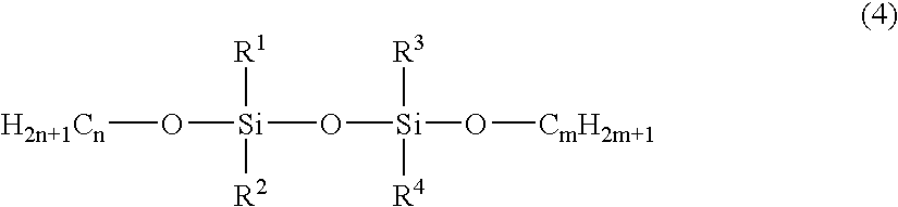
wherein R1, R2, R3 and R4 are one of CH3, C2H3, C2H5, C3H7 and C6H5, and m and n are any integer.

wherein R1, R2, R3, R4, R5 and R6 are one of CH3, C2H3, C2H5, C3H7 and C6H5, and the additive gases are argon (Ar), Helium (He) and either nitrogen oxide (N2O) or oxygen (O2).

wherein R1, R2, R3 and R4 are one of CH3, C2H3, C2H5, C3H7 and C6H5, and the additive gases are argon (Ar), Helium (He) and either nitrogen oxide (N2O) or oxygen (O2).
Rt[s]=9.42×10⁷(Pr·Ts/Ps·Tr)r w 2 d/F
-
- wherein:
- Pr: reaction chamber pressure (Pa)
- Ps: standard atmospheric pressure (Pa)
- Tr: average temperature of the reaction (K)
- Ts: standard temperature (K)
- rw: radius of the silicon substrate (m)
- d: space between the silicon substrate and the upper electrode (m)
- F: total flow volume of the reaction gas (sccm)

wherein X1 and X2 are OnCmHp wherein n is 0 or 1, m and p are integers including zero.
-
- rw (radius of the silicon substrate): 0.1 m
- d (space between the silicon substrate and the upper electrode): 0.024 m
- Ps (standard atmospheric pressure): 1.01×10⁵ Pa
- Ts (standard temperature): 273 K
-
- DMDMOS (dimethyl dimethoxysilane): 160 sccm
- IPA (isopropyl alcohol): 200 sccm
- He: 50 sccm
- Pr (reaction chamber pressure): 500 Pa
- RF power supply (HF: 13.4 MHz): 1600 W
- RF power supply (LF: 400 kHz): 200 W
- Tr (average temperature of the reaction): 673 K
- F (total flow volume of the reaction gas): 410 sccm
- Rt (residence time; Rt[s]=9.42×10⁷(Pr·Ts/Ps·Tr)rw 2d/F): 119 ms
-
- k (dielectric constant): 3.5
- Stress: −160 MPa
- Modulus: 35 GPa
- Hardness: 4.1 GPa
-
- DMDMOS (dimethyl dimethoxysilane): 160 sccm
- IPA (isopropyl alcohol): 0 sccm
- He: 150 sccm
- Pr (reaction chamber pressure): 533 Pa
- RF power supply (HF: 13.4 MHz): 1400 W
- RF power supply (LF: 400 kHz): 300 W
- Tr (average temperature of the reaction): 673 K
- F (total flow volume of the reaction gas): 310 sccm
- Rt (residence time; Rt[s]=9.42×10⁷(Pr·Ts/Ps·Tr)rw 2d/F): 168 ms
-
- k (dielectric constant): 3.4
- Stress: −180 MPa
- Modulus: 25 GPa
- Hardness: 3.1 GPa
-
- OMCTC (octamethylcyclotetrasiloxane): 160 sccm
- DVDVS ((CH3)2Si(C2H3)2): 80 sccm
- He: 100 sccm
- Pr (reaction chamber pressure): 467 Pa
- RF power supply (HF: 13.4 MHz): 1500 W
- RF power supply (LF: 400 kHz): 200 W
- Tr (average temperature of the reaction): 673 K
- F (total flow volume of the reaction gas): 340 sccm
- Rt (residence time; Rt[s]=9.42×10⁷(Pr·Ts/Ps·Tr)rw 2d/F): 120 ms
-
- k (dielectric constant): 3.5
- Stress: −190 MPa
- Modulus: 27 GPa
- Hardness: 3.3 GPa
-
- TMTVS ([CH2═CH(CH3)SiO]3): 140 sccm
- He: 100 sccm
- Pr (reaction chamber pressure): 360 Pa
- RF power supply (HF: 13.4 MHz): 200 W
- RF power supply (LF: 400 kHz): 50 W
- Tr (average temperature of the reaction): 673 K
- F (total flow volume of the reaction gas): 340 sccm
- Rt (residence time; Rt[s]=9.42×10⁷(Pr·Ts/Ps·Tr)rw 2d/F): 149 ms
-
- k (dielectric constant): 3.3
- Stress: −140 MPa
- Modulus: 23 GPa
- Hardness: 2.8 GPa
Rt[s]=9.42×10⁷(Pr·Ts/Ps·Tr)r w 2 d/F
-
- wherein Pr: reaction space pressure (Pa); Ps: standard atmospheric pressure (Pa); Tr: average temperature of the reaction (K); Ts: standard temperature (K); rw: radius of the silicon substrate (m); d: space between the silicon substrate and the upper electrode (m); F: total flow volume of the reaction gas (sccm).
Claims (31)
Rt[s]=9.42×10⁷(Pr·Ts/Ps·Tr)r w 2 d/F
Rt[s]=9.42×10⁷(Pr·Ts/Ps·Tr)r w 2 d/F
Rt[s]=9.42×10⁷(Pr·Ts/Ps·Tr)r w 2 d/F
Rt[s]=9.42×10⁷(Pr·Ts/Ps·Tr)r w 2 d/F
Priority Applications (4)
| Application Number | Priority Date | Filing Date | Title |
|---|---|---|---|
| US10/412,363 US7064088B2 (en) | 1998-02-05 | 2003-04-11 | Method for forming low-k hard film |
| US11/294,319 US7582575B2 (en) | 1998-02-05 | 2005-12-05 | Method for forming insulation film |
| US11/437,951 US20060258176A1 (en) | 1998-02-05 | 2006-05-19 | Method for forming insulation film |
| US11/465,751 US7354873B2 (en) | 1998-02-05 | 2006-08-18 | Method for forming insulation film |
Applications Claiming Priority (6)
| Application Number | Priority Date | Filing Date | Title |
|---|---|---|---|
| JP3792998 | 1998-02-05 | ||
| JP1998-37929 | 1998-02-05 | ||
| US24315699A | 1999-02-02 | 1999-02-02 | |
| US09/827,616 US6514880B2 (en) | 1998-02-05 | 2001-04-06 | Siloxan polymer film on semiconductor substrate and method for forming same |
| US10/317,239 US6881683B2 (en) | 1998-02-05 | 2002-12-11 | Insulation film on semiconductor substrate and method for forming same |
| US10/412,363 US7064088B2 (en) | 1998-02-05 | 2003-04-11 | Method for forming low-k hard film |
Related Parent Applications (1)
| Application Number | Title | Priority Date | Filing Date |
|---|---|---|---|
| US10/317,239 Continuation-In-Part US6881683B2 (en) | 1998-02-05 | 2002-12-11 | Insulation film on semiconductor substrate and method for forming same |
Related Child Applications (2)
| Application Number | Title | Priority Date | Filing Date |
|---|---|---|---|
| US11/294,319 Continuation-In-Part US7582575B2 (en) | 1998-02-05 | 2005-12-05 | Method for forming insulation film |
| US11/437,951 Continuation-In-Part US20060258176A1 (en) | 1998-02-05 | 2006-05-19 | Method for forming insulation film |
Publications (2)
| Publication Number | Publication Date |
|---|---|
| US20040038514A1 US20040038514A1 (en) | 2004-02-26 |
| US7064088B2 true US7064088B2 (en) | 2006-06-20 |
Family
ID=31892163
Family Applications (1)
| Application Number | Title | Priority Date | Filing Date |
|---|---|---|---|
| US10/412,363 Expired - Lifetime US7064088B2 (en) | 1998-02-05 | 2003-04-11 | Method for forming low-k hard film |
Country Status (1)
| Country | Link |
|---|---|
| US (1) | US7064088B2 (en) |
Cited By (40)
| Publication number | Priority date | Publication date | Assignee | Title |
|---|---|---|---|---|
| US20040253378A1 (en) * | 2003-06-12 | 2004-12-16 | Applied Materials, Inc. | Stress reduction of SIOC low k film by addition of alkylenes to OMCTS based processes |
| US20050037153A1 (en) * | 2003-08-14 | 2005-02-17 | Applied Materials, Inc. | Stress reduction of sioc low k films |
| US20060110931A1 (en) * | 1998-02-05 | 2006-05-25 | Asm Japan K.K. | Method for forming insulation film |
| US20060258176A1 (en) * | 1998-02-05 | 2006-11-16 | Asm Japan K.K. | Method for forming insulation film |
| US20070004204A1 (en) * | 1998-02-05 | 2007-01-04 | Asm Japan K.K. | Method for forming insulation film |
| US20070066086A1 (en) * | 2003-08-20 | 2007-03-22 | Asm Japan K.K. | Method of forming silicon-containing insulation film having low dielectric constant and low film stress |
| US7239017B1 (en) | 2003-09-24 | 2007-07-03 | Novellus Systems, Inc. | Low-k B-doped SiC copper diffusion barrier films |
| US7282438B1 (en) | 2004-06-15 | 2007-10-16 | Novellus Systems, Inc. | Low-k SiC copper diffusion barrier films |
| US20080076266A1 (en) * | 2006-09-21 | 2008-03-27 | Asm Japan K.K. | Method for forming insulation film having high density |
| US7390537B1 (en) | 2003-11-20 | 2008-06-24 | Novellus Systems, Inc. | Methods for producing low-k CDO films with low residual stress |
| US7420275B1 (en) | 2003-09-24 | 2008-09-02 | Novellus Systems, Inc. | Boron-doped SIC copper diffusion barrier films |
| US20080274627A1 (en) * | 2007-05-01 | 2008-11-06 | Shin-Etsu Chemical Co., Ltd. | Silicon-containing film, forming material, making method, and semiconductor device |
| US20080305648A1 (en) * | 2007-06-06 | 2008-12-11 | Asm Japan K.K. | Method for forming inorganic silazane-based dielectric film |
| US7473653B1 (en) | 2003-03-31 | 2009-01-06 | Novellus Systems, Inc. | Methods for producing low stress porous low-k dielectric materials using precursors with organic functional groups |
| US7622369B1 (en) | 2008-05-30 | 2009-11-24 | Asm Japan K.K. | Device isolation technology on semiconductor substrate |
| US7651959B2 (en) | 2007-12-03 | 2010-01-26 | Asm Japan K.K. | Method for forming silazane-based dielectric film |
| US7695765B1 (en) * | 2004-11-12 | 2010-04-13 | Novellus Systems, Inc. | Methods for producing low-stress carbon-doped oxide films with improved integration properties |
| US20100136789A1 (en) * | 2008-12-01 | 2010-06-03 | Air Products And Chemicals, Inc. | Dielectric Barrier Deposition Using Oxygen Containing Precursor |
| US20100143609A1 (en) * | 2008-12-09 | 2010-06-10 | Asm Japan K.K. | Method for forming low-carbon cvd film for filling trenches |
| US7737525B1 (en) | 2004-03-11 | 2010-06-15 | Novellus Systems, Inc. | Method for producing low-K CDO films |
| US20100174103A1 (en) * | 2007-02-14 | 2010-07-08 | Jsr Corporation | Material for forming silicon-containing film, and silicon-containing insulating film and method for forming the same |
| US7781351B1 (en) * | 2004-04-07 | 2010-08-24 | Novellus Systems, Inc. | Methods for producing low-k carbon doped oxide films with low residual stress |
| US20100261925A1 (en) * | 2007-07-10 | 2010-10-14 | Jsr Corporation | Method for producing silicon compound |
| US20110042789A1 (en) * | 2008-03-26 | 2011-02-24 | Jsr Corporation | Material for chemical vapor deposition, silicon-containing insulating film and method for production of the silicon-containing insulating film |
| US7906174B1 (en) | 2006-12-07 | 2011-03-15 | Novellus Systems, Inc. | PECVD methods for producing ultra low-k dielectric films using UV treatment |
| US7915166B1 (en) | 2007-02-22 | 2011-03-29 | Novellus Systems, Inc. | Diffusion barrier and etch stop films |
| US20110135557A1 (en) * | 2009-12-04 | 2011-06-09 | Vishwanathan Rangarajan | Hardmask materials |
| US7972976B1 (en) | 2005-01-31 | 2011-07-05 | Novellus Systems, Inc. | VLSI fabrication processes for introducing pores into dielectric materials |
| US8124522B1 (en) | 2008-04-11 | 2012-02-28 | Novellus Systems, Inc. | Reducing UV and dielectric diffusion barrier interaction through the modulation of optical properties |
| US8173537B1 (en) | 2007-03-29 | 2012-05-08 | Novellus Systems, Inc. | Methods for reducing UV and dielectric diffusion barrier interaction |
| US8637412B2 (en) | 2011-08-19 | 2014-01-28 | International Business Machines Corporation | Process to form an adhesion layer and multiphase ultra-low k dielectric material using PECVD |
| US9234276B2 (en) | 2013-05-31 | 2016-01-12 | Novellus Systems, Inc. | Method to obtain SiC class of films of desired composition and film properties |
| US9337068B2 (en) | 2012-12-18 | 2016-05-10 | Lam Research Corporation | Oxygen-containing ceramic hard masks and associated wet-cleans |
| US9837270B1 (en) | 2016-12-16 | 2017-12-05 | Lam Research Corporation | Densification of silicon carbide film using remote plasma treatment |
| US10002787B2 (en) | 2016-11-23 | 2018-06-19 | Lam Research Corporation | Staircase encapsulation in 3D NAND fabrication |
| US10211310B2 (en) | 2012-06-12 | 2019-02-19 | Novellus Systems, Inc. | Remote plasma based deposition of SiOC class of films |
| US10297442B2 (en) | 2013-05-31 | 2019-05-21 | Lam Research Corporation | Remote plasma based deposition of graded or multi-layered silicon carbide film |
| US10325773B2 (en) | 2012-06-12 | 2019-06-18 | Novellus Systems, Inc. | Conformal deposition of silicon carbide films |
| US10832904B2 (en) | 2012-06-12 | 2020-11-10 | Lam Research Corporation | Remote plasma based deposition of oxygen doped silicon carbide films |
| US11049716B2 (en) | 2015-04-21 | 2021-06-29 | Lam Research Corporation | Gap fill using carbon-based films |
Families Citing this family (20)
| Publication number | Priority date | Publication date | Assignee | Title |
|---|---|---|---|---|
| US6593247B1 (en) * | 1998-02-11 | 2003-07-15 | Applied Materials, Inc. | Method of depositing low k films using an oxidizing plasma |
| US6486082B1 (en) * | 2001-06-18 | 2002-11-26 | Applied Materials, Inc. | CVD plasma assisted lower dielectric constant sicoh film |
| US7025748B2 (en) * | 2001-11-08 | 2006-04-11 | Boston Scientific Scimed, Inc. | Sheath based blood vessel puncture locator and depth indicator |
| US20030194495A1 (en) * | 2002-04-11 | 2003-10-16 | Applied Materials, Inc. | Crosslink cyclo-siloxane compound with linear bridging group to form ultra low k dielectric |
| US6815373B2 (en) | 2002-04-16 | 2004-11-09 | Applied Materials Inc. | Use of cyclic siloxanes for hardness improvement of low k dielectric films |
| US7060330B2 (en) | 2002-05-08 | 2006-06-13 | Applied Materials, Inc. | Method for forming ultra low k films using electron beam |
| US6936551B2 (en) * | 2002-05-08 | 2005-08-30 | Applied Materials Inc. | Methods and apparatus for E-beam treatment used to fabricate integrated circuit devices |
| US7056560B2 (en) * | 2002-05-08 | 2006-06-06 | Applies Materials Inc. | Ultra low dielectric materials based on hybrid system of linear silicon precursor and organic porogen by plasma-enhanced chemical vapor deposition (PECVD) |
| US20040101632A1 (en) * | 2002-11-22 | 2004-05-27 | Applied Materials, Inc. | Method for curing low dielectric constant film by electron beam |
| JP4334844B2 (en) * | 2002-06-26 | 2009-09-30 | 東京エレクトロン株式会社 | Manufacturing method of groove structure for device |
| US6797643B2 (en) * | 2002-10-23 | 2004-09-28 | Applied Materials Inc. | Plasma enhanced CVD low k carbon-doped silicon oxide film deposition using VHF-RF power |
| US6897163B2 (en) * | 2003-01-31 | 2005-05-24 | Applied Materials, Inc. | Method for depositing a low dielectric constant film |
| WO2005004221A2 (en) * | 2003-07-08 | 2005-01-13 | Silecs Oy | Low-k-dielectric material |
| JP2005294333A (en) * | 2004-03-31 | 2005-10-20 | Semiconductor Process Laboratory Co Ltd | Film depositing method and semiconductor device |
| US7560144B2 (en) * | 2005-03-22 | 2009-07-14 | Asm Japan K.K. | Method of stabilizing film quality of low-dielectric constant film |
| US7674521B2 (en) * | 2005-07-27 | 2010-03-09 | International Business Machines Corporation | Materials containing voids with void size controlled on the nanometer scale |
| US20070134435A1 (en) * | 2005-12-13 | 2007-06-14 | Ahn Sang H | Method to improve the ashing/wet etch damage resistance and integration stability of low dielectric constant films |
| US7297376B1 (en) | 2006-07-07 | 2007-11-20 | Applied Materials, Inc. | Method to reduce gas-phase reactions in a PECVD process with silicon and organic precursors to deposit defect-free initial layers |
| US8741394B2 (en) | 2010-03-25 | 2014-06-03 | Novellus Systems, Inc. | In-situ deposition of film stacks |
| US20110244142A1 (en) * | 2010-03-30 | 2011-10-06 | Applied Materials, Inc. | Nitrogen doped amorphous carbon hardmask |
Citations (10)
| Publication number | Priority date | Publication date | Assignee | Title |
|---|---|---|---|---|
| US6352945B1 (en) | 1998-02-05 | 2002-03-05 | Asm Japan K.K. | Silicone polymer insulation film on semiconductor substrate and method for forming the film |
| US6383955B1 (en) | 1998-02-05 | 2002-05-07 | Asm Japan K.K. | Silicone polymer insulation film on semiconductor substrate and method for forming the film |
| EP1225194A2 (en) | 2001-01-17 | 2002-07-24 | Air Products And Chemicals, Inc. | Method of forming a dielectric interlayer film with organosilicon precursors |
| US6432846B1 (en) | 1999-02-02 | 2002-08-13 | Asm Japan K.K. | Silicone polymer insulation film on semiconductor substrate and method for forming the film |
| US6436822B1 (en) | 2000-11-20 | 2002-08-20 | Intel Corporation | Method for making a carbon doped oxide dielectric material |
| US6514880B2 (en) | 1998-02-05 | 2003-02-04 | Asm Japan K.K. | Siloxan polymer film on semiconductor substrate and method for forming same |
| US20030100175A1 (en) * | 2001-10-09 | 2003-05-29 | Mitsubishi Denki Kabushiki Kaisha | Low dielectric constant material, process for preparing the same, insulating film comprising the same and semiconductor device |
| US20030194880A1 (en) * | 2002-04-16 | 2003-10-16 | Applied Materials, Inc. | Use of cyclic siloxanes for hardness improvement |
| US20040137757A1 (en) * | 2003-01-13 | 2004-07-15 | Applied Materials, Inc. | Method and apparatus to improve cracking thresholds and mechanical properties of low-k dielectric material |
| US6818570B2 (en) * | 2002-03-04 | 2004-11-16 | Asm Japan K.K. | Method of forming silicon-containing insulation film having low dielectric constant and high mechanical strength |
-
2003
- 2003-04-11 US US10/412,363 patent/US7064088B2/en not_active Expired - Lifetime
Patent Citations (12)
| Publication number | Priority date | Publication date | Assignee | Title |
|---|---|---|---|---|
| US6352945B1 (en) | 1998-02-05 | 2002-03-05 | Asm Japan K.K. | Silicone polymer insulation film on semiconductor substrate and method for forming the film |
| US6383955B1 (en) | 1998-02-05 | 2002-05-07 | Asm Japan K.K. | Silicone polymer insulation film on semiconductor substrate and method for forming the film |
| US6410463B1 (en) | 1998-02-05 | 2002-06-25 | Asm Japan K.K. | Method for forming film with low dielectric constant on semiconductor substrate |
| US6455445B2 (en) | 1998-02-05 | 2002-09-24 | Asm Japan K.K. | Silicone polymer insulation film on semiconductor substrate and method for forming the film |
| US6514880B2 (en) | 1998-02-05 | 2003-02-04 | Asm Japan K.K. | Siloxan polymer film on semiconductor substrate and method for forming same |
| US6432846B1 (en) | 1999-02-02 | 2002-08-13 | Asm Japan K.K. | Silicone polymer insulation film on semiconductor substrate and method for forming the film |
| US6436822B1 (en) | 2000-11-20 | 2002-08-20 | Intel Corporation | Method for making a carbon doped oxide dielectric material |
| EP1225194A2 (en) | 2001-01-17 | 2002-07-24 | Air Products And Chemicals, Inc. | Method of forming a dielectric interlayer film with organosilicon precursors |
| US20030100175A1 (en) * | 2001-10-09 | 2003-05-29 | Mitsubishi Denki Kabushiki Kaisha | Low dielectric constant material, process for preparing the same, insulating film comprising the same and semiconductor device |
| US6818570B2 (en) * | 2002-03-04 | 2004-11-16 | Asm Japan K.K. | Method of forming silicon-containing insulation film having low dielectric constant and high mechanical strength |
| US20030194880A1 (en) * | 2002-04-16 | 2003-10-16 | Applied Materials, Inc. | Use of cyclic siloxanes for hardness improvement |
| US20040137757A1 (en) * | 2003-01-13 | 2004-07-15 | Applied Materials, Inc. | Method and apparatus to improve cracking thresholds and mechanical properties of low-k dielectric material |
Non-Patent Citations (3)
| Title |
|---|
| U.S. Appl. No. 10/317,239, filed Dec. 11, 2002, Matsuki et al. |
| U.S. Appl. No. 10/351,669, filed Jan. 24, 2003, Tsuji et al. |
| U.S. Appl. No. 10/402,109, filed Mar. 27, 2003, Matsuki et al. |
Cited By (61)
| Publication number | Priority date | Publication date | Assignee | Title |
|---|---|---|---|---|
| US7354873B2 (en) | 1998-02-05 | 2008-04-08 | Asm Japan K.K. | Method for forming insulation film |
| US7582575B2 (en) * | 1998-02-05 | 2009-09-01 | Asm Japan K.K. | Method for forming insulation film |
| US20060110931A1 (en) * | 1998-02-05 | 2006-05-25 | Asm Japan K.K. | Method for forming insulation film |
| US20060258176A1 (en) * | 1998-02-05 | 2006-11-16 | Asm Japan K.K. | Method for forming insulation film |
| US20070004204A1 (en) * | 1998-02-05 | 2007-01-04 | Asm Japan K.K. | Method for forming insulation film |
| US7473653B1 (en) | 2003-03-31 | 2009-01-06 | Novellus Systems, Inc. | Methods for producing low stress porous low-k dielectric materials using precursors with organic functional groups |
| US20090239390A1 (en) * | 2003-03-31 | 2009-09-24 | Novellus Systems, Inc. | Methods for producing low stress porous and cdo low-k dielectric materials using precursors with organic functional groups |
| US7923385B2 (en) | 2003-03-31 | 2011-04-12 | Novellus Systems, Inc. | Methods for producing low stress porous and CDO low-K dielectric materials using precursors with organic functional groups |
| US7799705B1 (en) | 2003-03-31 | 2010-09-21 | Novellus Systems, Inc. | Methods for producing low stress porous low-k dielectric materials using precursors with organic functional groups |
| US20040253378A1 (en) * | 2003-06-12 | 2004-12-16 | Applied Materials, Inc. | Stress reduction of SIOC low k film by addition of alkylenes to OMCTS based processes |
| US20050037153A1 (en) * | 2003-08-14 | 2005-02-17 | Applied Materials, Inc. | Stress reduction of sioc low k films |
| US7655577B2 (en) | 2003-08-20 | 2010-02-02 | Asm Japan K.K. | Method of forming silicon-containing insulation film having low dielectric constant and low film stress |
| US20070111540A1 (en) * | 2003-08-20 | 2007-05-17 | Asm Japan K.K. | Method of forming silicon-containing insulation film having low dielectric constant and low film stress |
| US20070066086A1 (en) * | 2003-08-20 | 2007-03-22 | Asm Japan K.K. | Method of forming silicon-containing insulation film having low dielectric constant and low film stress |
| US7842604B1 (en) | 2003-09-24 | 2010-11-30 | Novellus Systems, Inc. | Low-k b-doped SiC copper diffusion barrier films |
| US7420275B1 (en) | 2003-09-24 | 2008-09-02 | Novellus Systems, Inc. | Boron-doped SIC copper diffusion barrier films |
| US7239017B1 (en) | 2003-09-24 | 2007-07-03 | Novellus Systems, Inc. | Low-k B-doped SiC copper diffusion barrier films |
| US7390537B1 (en) | 2003-11-20 | 2008-06-24 | Novellus Systems, Inc. | Methods for producing low-k CDO films with low residual stress |
| US7737525B1 (en) | 2004-03-11 | 2010-06-15 | Novellus Systems, Inc. | Method for producing low-K CDO films |
| US7781351B1 (en) * | 2004-04-07 | 2010-08-24 | Novellus Systems, Inc. | Methods for producing low-k carbon doped oxide films with low residual stress |
| US7573061B1 (en) | 2004-06-15 | 2009-08-11 | Novellus Systems, Inc. | Low-k SiC copper diffusion barrier films |
| US7968436B1 (en) | 2004-06-15 | 2011-06-28 | Novellus Systems, Inc. | Low-K SiC copper diffusion barrier films |
| US7282438B1 (en) | 2004-06-15 | 2007-10-16 | Novellus Systems, Inc. | Low-k SiC copper diffusion barrier films |
| US7695765B1 (en) * | 2004-11-12 | 2010-04-13 | Novellus Systems, Inc. | Methods for producing low-stress carbon-doped oxide films with improved integration properties |
| US7972976B1 (en) | 2005-01-31 | 2011-07-05 | Novellus Systems, Inc. | VLSI fabrication processes for introducing pores into dielectric materials |
| US20080076266A1 (en) * | 2006-09-21 | 2008-03-27 | Asm Japan K.K. | Method for forming insulation film having high density |
| US7718553B2 (en) | 2006-09-21 | 2010-05-18 | Asm Japan K.K. | Method for forming insulation film having high density |
| US7906174B1 (en) | 2006-12-07 | 2011-03-15 | Novellus Systems, Inc. | PECVD methods for producing ultra low-k dielectric films using UV treatment |
| US20100174103A1 (en) * | 2007-02-14 | 2010-07-08 | Jsr Corporation | Material for forming silicon-containing film, and silicon-containing insulating film and method for forming the same |
| US8669181B1 (en) | 2007-02-22 | 2014-03-11 | Novellus Systems, Inc. | Diffusion barrier and etch stop films |
| US7915166B1 (en) | 2007-02-22 | 2011-03-29 | Novellus Systems, Inc. | Diffusion barrier and etch stop films |
| US8173537B1 (en) | 2007-03-29 | 2012-05-08 | Novellus Systems, Inc. | Methods for reducing UV and dielectric diffusion barrier interaction |
| US20080274627A1 (en) * | 2007-05-01 | 2008-11-06 | Shin-Etsu Chemical Co., Ltd. | Silicon-containing film, forming material, making method, and semiconductor device |
| US20080305648A1 (en) * | 2007-06-06 | 2008-12-11 | Asm Japan K.K. | Method for forming inorganic silazane-based dielectric film |
| US7781352B2 (en) | 2007-06-06 | 2010-08-24 | Asm Japan K.K. | Method for forming inorganic silazane-based dielectric film |
| US20100261925A1 (en) * | 2007-07-10 | 2010-10-14 | Jsr Corporation | Method for producing silicon compound |
| US7651959B2 (en) | 2007-12-03 | 2010-01-26 | Asm Japan K.K. | Method for forming silazane-based dielectric film |
| US20110042789A1 (en) * | 2008-03-26 | 2011-02-24 | Jsr Corporation | Material for chemical vapor deposition, silicon-containing insulating film and method for production of the silicon-containing insulating film |
| US8124522B1 (en) | 2008-04-11 | 2012-02-28 | Novellus Systems, Inc. | Reducing UV and dielectric diffusion barrier interaction through the modulation of optical properties |
| US20090298257A1 (en) * | 2008-05-30 | 2009-12-03 | Asm Japan K.K. | Device isolation technology on semiconductor substrate |
| US7622369B1 (en) | 2008-05-30 | 2009-11-24 | Asm Japan K.K. | Device isolation technology on semiconductor substrate |
| US20100136789A1 (en) * | 2008-12-01 | 2010-06-03 | Air Products And Chemicals, Inc. | Dielectric Barrier Deposition Using Oxygen Containing Precursor |
| US8637396B2 (en) | 2008-12-01 | 2014-01-28 | Air Products And Chemicals, Inc. | Dielectric barrier deposition using oxygen containing precursor |
| US20100143609A1 (en) * | 2008-12-09 | 2010-06-10 | Asm Japan K.K. | Method for forming low-carbon cvd film for filling trenches |
| US8765233B2 (en) | 2008-12-09 | 2014-07-01 | Asm Japan K.K. | Method for forming low-carbon CVD film for filling trenches |
| US8846525B2 (en) | 2009-12-04 | 2014-09-30 | Novellus Systems, Inc. | Hardmask materials |
| US8247332B2 (en) | 2009-12-04 | 2012-08-21 | Novellus Systems, Inc. | Hardmask materials |
| US20110135557A1 (en) * | 2009-12-04 | 2011-06-09 | Vishwanathan Rangarajan | Hardmask materials |
| US8637412B2 (en) | 2011-08-19 | 2014-01-28 | International Business Machines Corporation | Process to form an adhesion layer and multiphase ultra-low k dielectric material using PECVD |
| US10325773B2 (en) | 2012-06-12 | 2019-06-18 | Novellus Systems, Inc. | Conformal deposition of silicon carbide films |
| US11264234B2 (en) | 2012-06-12 | 2022-03-01 | Novellus Systems, Inc. | Conformal deposition of silicon carbide films |
| US10832904B2 (en) | 2012-06-12 | 2020-11-10 | Lam Research Corporation | Remote plasma based deposition of oxygen doped silicon carbide films |
| US10211310B2 (en) | 2012-06-12 | 2019-02-19 | Novellus Systems, Inc. | Remote plasma based deposition of SiOC class of films |
| US9337068B2 (en) | 2012-12-18 | 2016-05-10 | Lam Research Corporation | Oxygen-containing ceramic hard masks and associated wet-cleans |
| US9234276B2 (en) | 2013-05-31 | 2016-01-12 | Novellus Systems, Inc. | Method to obtain SiC class of films of desired composition and film properties |
| US10297442B2 (en) | 2013-05-31 | 2019-05-21 | Lam Research Corporation | Remote plasma based deposition of graded or multi-layered silicon carbide film |
| US10472714B2 (en) | 2013-05-31 | 2019-11-12 | Novellus Systems, Inc. | Method to obtain SiC class of films of desired composition and film properties |
| US11049716B2 (en) | 2015-04-21 | 2021-06-29 | Lam Research Corporation | Gap fill using carbon-based films |
| US10580690B2 (en) | 2016-11-23 | 2020-03-03 | Lam Research Corporation | Staircase encapsulation in 3D NAND fabrication |
| US10002787B2 (en) | 2016-11-23 | 2018-06-19 | Lam Research Corporation | Staircase encapsulation in 3D NAND fabrication |
| US9837270B1 (en) | 2016-12-16 | 2017-12-05 | Lam Research Corporation | Densification of silicon carbide film using remote plasma treatment |
Also Published As
| Publication number | Publication date |
|---|---|
| US20040038514A1 (en) | 2004-02-26 |
Similar Documents
| Publication | Publication Date | Title |
|---|---|---|
| US7064088B2 (en) | Method for forming low-k hard film | |
| US6881683B2 (en) | Insulation film on semiconductor substrate and method for forming same | |
| US6740602B1 (en) | Method of forming low-dielectric constant film on semiconductor substrate by plasma reaction using high-RF power | |
| US7582575B2 (en) | Method for forming insulation film | |
| US6352945B1 (en) | Silicone polymer insulation film on semiconductor substrate and method for forming the film | |
| US6432846B1 (en) | Silicone polymer insulation film on semiconductor substrate and method for forming the film | |
| US7354873B2 (en) | Method for forming insulation film | |
| US6852650B2 (en) | Insulation film on semiconductor substrate and method for forming same | |
| US6410463B1 (en) | Method for forming film with low dielectric constant on semiconductor substrate | |
| US7524735B1 (en) | Flowable film dielectric gap fill process | |
| US6514880B2 (en) | Siloxan polymer film on semiconductor substrate and method for forming same | |
| US6818570B2 (en) | Method of forming silicon-containing insulation film having low dielectric constant and high mechanical strength | |
| US20060258176A1 (en) | Method for forming insulation film | |
| US7655577B2 (en) | Method of forming silicon-containing insulation film having low dielectric constant and low film stress | |
| US6784123B2 (en) | Insulation film on semiconductor substrate and method for forming same | |
| US20080274627A1 (en) | Silicon-containing film, forming material, making method, and semiconductor device | |
| WO2001036703A1 (en) | System and method for depositing inorganic/organic dielectric films | |
| EP1396884A2 (en) | Interlayer insulation film used for multilayer interconnect of semiconductor integrated circuit and method of manufacturing the same | |
| US7585789B2 (en) | Method for forming porous insulation film | |
| JP3197007B2 (en) | Silicon polymer insulating film on semiconductor substrate and method for forming the film | |
| JP3781730B2 (en) | Method for forming silicon insulating film having low dielectric constant and high mechanical strength | |
| JP4651076B2 (en) | Method for forming an insulating film on a semiconductor substrate | |
| JP2002329718A (en) | Siloxane polymer film on semiconductor substrate and its manufacturing method |
Legal Events
| Date | Code | Title | Description |
|---|---|---|---|
| AS | Assignment |
Owner name: ASM JAPAN K.K., JAPAN Free format text: ASSIGNMENT OF ASSIGNORS INTEREST;ASSIGNORS:HYODO, YASUYOSHI;FUKAZAWA, ATSUKI;MORISADA, YOSHINORI;AND OTHERS;REEL/FRAME:014232/0698;SIGNING DATES FROM 20030507 TO 20030509 |
|
| STCF | Information on status: patent grant |
Free format text: PATENTED CASE |
|
| FEPP | Fee payment procedure |
Free format text: PAYER NUMBER DE-ASSIGNED (ORIGINAL EVENT CODE: RMPN); ENTITY STATUS OF PATENT OWNER: LARGE ENTITY Free format text: PAYOR NUMBER ASSIGNED (ORIGINAL EVENT CODE: ASPN); ENTITY STATUS OF PATENT OWNER: LARGE ENTITY |
|
| FPAY | Fee payment |
Year of fee payment: 4 |
|
| FPAY | Fee payment |
Year of fee payment: 8 |
|
| MAFP | Maintenance fee payment |
Free format text: PAYMENT OF MAINTENANCE FEE, 12TH YEAR, LARGE ENTITY (ORIGINAL EVENT CODE: M1553) Year of fee payment: 12 |