US7030412B1 - Minimally-patterned semiconductor devices for display applications - Google Patents
Minimally-patterned semiconductor devices for display applications Download PDFInfo
- Publication number
- US7030412B1 US7030412B1 US09/565,413 US56541300A US7030412B1 US 7030412 B1 US7030412 B1 US 7030412B1 US 56541300 A US56541300 A US 56541300A US 7030412 B1 US7030412 B1 US 7030412B1
- Authority
- US
- United States
- Prior art keywords
- transistor
- electrode
- thin
- semiconductor layer
- data line
- Prior art date
- Legal status (The legal status is an assumption and is not a legal conclusion. Google has not performed a legal analysis and makes no representation as to the accuracy of the status listed.)
- Expired - Fee Related
Links
- 239000004065 semiconductor Substances 0.000 title claims abstract description 64
- 239000010409 thin film Substances 0.000 claims abstract description 38
- 239000000463 material Substances 0.000 claims description 65
- 229910021417 amorphous silicon Inorganic materials 0.000 claims description 21
- 238000004891 communication Methods 0.000 claims description 19
- XUIMIQQOPSSXEZ-UHFFFAOYSA-N Silicon Chemical compound [Si] XUIMIQQOPSSXEZ-UHFFFAOYSA-N 0.000 claims description 4
- 238000002161 passivation Methods 0.000 claims description 4
- 229910052710 silicon Inorganic materials 0.000 claims description 4
- 239000010703 silicon Substances 0.000 claims description 4
- 239000002019 doping agent Substances 0.000 claims description 3
- 239000002245 particle Substances 0.000 description 109
- 238000000034 method Methods 0.000 description 53
- 239000002775 capsule Substances 0.000 description 45
- 229920000642 polymer Polymers 0.000 description 40
- 239000000976 ink Substances 0.000 description 38
- 239000000049 pigment Substances 0.000 description 36
- 230000008569 process Effects 0.000 description 35
- 239000012530 fluid Substances 0.000 description 34
- -1 poly(3,4-ethylenedioxythiophene) Polymers 0.000 description 33
- 239000000758 substrate Substances 0.000 description 27
- 239000000975 dye Substances 0.000 description 24
- 230000003287 optical effect Effects 0.000 description 21
- 239000007788 liquid Substances 0.000 description 20
- 239000002609 medium Substances 0.000 description 20
- 238000000576 coating method Methods 0.000 description 19
- 239000012071 phase Substances 0.000 description 17
- GWEVSGVZZGPLCZ-UHFFFAOYSA-N Titan oxide Chemical compound O=[Ti]=O GWEVSGVZZGPLCZ-UHFFFAOYSA-N 0.000 description 16
- 239000004020 conductor Substances 0.000 description 16
- 239000011248 coating agent Substances 0.000 description 15
- 238000004519 manufacturing process Methods 0.000 description 15
- 239000000203 mixture Substances 0.000 description 15
- WSFSSNUMVMOOMR-UHFFFAOYSA-N Formaldehyde Chemical compound O=C WSFSSNUMVMOOMR-UHFFFAOYSA-N 0.000 description 14
- 239000011230 binding agent Substances 0.000 description 13
- 239000003795 chemical substances by application Substances 0.000 description 13
- 239000002904 solvent Substances 0.000 description 13
- XLYOFNOQVPJJNP-UHFFFAOYSA-N water Substances O XLYOFNOQVPJJNP-UHFFFAOYSA-N 0.000 description 13
- 239000003921 oil Substances 0.000 description 12
- 229920005989 resin Polymers 0.000 description 12
- 239000011347 resin Substances 0.000 description 12
- 239000000126 substance Substances 0.000 description 10
- 230000005684 electric field Effects 0.000 description 9
- 229910052751 metal Inorganic materials 0.000 description 9
- 239000002184 metal Substances 0.000 description 9
- 239000000178 monomer Substances 0.000 description 9
- 238000005538 encapsulation Methods 0.000 description 8
- LYCAIKOWRPUZTN-UHFFFAOYSA-N Ethylene glycol Chemical group OCCO LYCAIKOWRPUZTN-UHFFFAOYSA-N 0.000 description 7
- PPBRXRYQALVLMV-UHFFFAOYSA-N Styrene Chemical compound C=CC1=CC=CC=C1 PPBRXRYQALVLMV-UHFFFAOYSA-N 0.000 description 7
- 239000006185 dispersion Substances 0.000 description 7
- 239000003094 microcapsule Substances 0.000 description 7
- 230000037230 mobility Effects 0.000 description 7
- 238000006116 polymerization reaction Methods 0.000 description 7
- ZOXJGFHDIHLPTG-UHFFFAOYSA-N Boron Chemical compound [B] ZOXJGFHDIHLPTG-UHFFFAOYSA-N 0.000 description 6
- OKTJSMMVPCPJKN-UHFFFAOYSA-N Carbon Chemical compound [C] OKTJSMMVPCPJKN-UHFFFAOYSA-N 0.000 description 6
- VYPSYNLAJGMNEJ-UHFFFAOYSA-N Silicium dioxide Chemical compound O=[Si]=O VYPSYNLAJGMNEJ-UHFFFAOYSA-N 0.000 description 6
- 229910052796 boron Inorganic materials 0.000 description 6
- 230000008859 change Effects 0.000 description 6
- 238000013461 design Methods 0.000 description 6
- 239000004973 liquid crystal related substance Substances 0.000 description 6
- XSQUKJJJFZCRTK-UHFFFAOYSA-N Urea Chemical compound NC(N)=O XSQUKJJJFZCRTK-UHFFFAOYSA-N 0.000 description 5
- 239000008346 aqueous phase Substances 0.000 description 5
- 239000004202 carbamide Substances 0.000 description 5
- 238000005354 coacervation Methods 0.000 description 5
- 229920001577 copolymer Polymers 0.000 description 5
- 239000000839 emulsion Substances 0.000 description 5
- 238000011065 in-situ storage Methods 0.000 description 5
- 229920000126 latex Polymers 0.000 description 5
- 238000005191 phase separation Methods 0.000 description 5
- 238000007639 printing Methods 0.000 description 5
- 241000894007 species Species 0.000 description 5
- 230000006641 stabilisation Effects 0.000 description 5
- 238000011105 stabilization Methods 0.000 description 5
- 239000003381 stabilizer Substances 0.000 description 5
- 239000004094 surface-active agent Substances 0.000 description 5
- 150000001412 amines Chemical group 0.000 description 4
- 239000003990 capacitor Substances 0.000 description 4
- 239000006229 carbon black Substances 0.000 description 4
- 238000000151 deposition Methods 0.000 description 4
- AMGQUBHHOARCQH-UHFFFAOYSA-N indium;oxotin Chemical compound [In].[Sn]=O AMGQUBHHOARCQH-UHFFFAOYSA-N 0.000 description 4
- 229910044991 metal oxide Inorganic materials 0.000 description 4
- 150000004706 metal oxides Chemical class 0.000 description 4
- 239000003607 modifier Substances 0.000 description 4
- 239000003960 organic solvent Substances 0.000 description 4
- 238000000059 patterning Methods 0.000 description 4
- 229920003229 poly(methyl methacrylate) Polymers 0.000 description 4
- 229920000728 polyester Polymers 0.000 description 4
- 229920001296 polysiloxane Polymers 0.000 description 4
- 229920000123 polythiophene Polymers 0.000 description 4
- OYPRJOBELJOOCE-UHFFFAOYSA-N Calcium Chemical compound [Ca] OYPRJOBELJOOCE-UHFFFAOYSA-N 0.000 description 3
- SNRUBQQJIBEYMU-UHFFFAOYSA-N Dodecane Natural products CCCCCCCCCCCC SNRUBQQJIBEYMU-UHFFFAOYSA-N 0.000 description 3
- 108010010803 Gelatin Proteins 0.000 description 3
- PEDCQBHIVMGVHV-UHFFFAOYSA-N Glycerine Chemical compound OCC(O)CO PEDCQBHIVMGVHV-UHFFFAOYSA-N 0.000 description 3
- 238000012695 Interfacial polymerization Methods 0.000 description 3
- VVQNEPGJFQJSBK-UHFFFAOYSA-N Methyl methacrylate Chemical compound COC(=O)C(C)=C VVQNEPGJFQJSBK-UHFFFAOYSA-N 0.000 description 3
- 239000004642 Polyimide Substances 0.000 description 3
- 239000004793 Polystyrene Substances 0.000 description 3
- BQCADISMDOOEFD-UHFFFAOYSA-N Silver Chemical compound [Ag] BQCADISMDOOEFD-UHFFFAOYSA-N 0.000 description 3
- YXFVVABEGXRONW-UHFFFAOYSA-N Toluene Chemical compound CC1=CC=CC=C1 YXFVVABEGXRONW-UHFFFAOYSA-N 0.000 description 3
- 239000000654 additive Substances 0.000 description 3
- 239000002671 adjuvant Substances 0.000 description 3
- 229910052791 calcium Inorganic materials 0.000 description 3
- 239000011575 calcium Substances 0.000 description 3
- 239000002131 composite material Substances 0.000 description 3
- 150000001875 compounds Chemical class 0.000 description 3
- 229920001940 conductive polymer Polymers 0.000 description 3
- 239000003431 cross linking reagent Substances 0.000 description 3
- 230000008021 deposition Effects 0.000 description 3
- 238000012674 dispersion polymerization Methods 0.000 description 3
- 238000009826 distribution Methods 0.000 description 3
- 229920000159 gelatin Polymers 0.000 description 3
- 235000019322 gelatine Nutrition 0.000 description 3
- 235000011852 gelatine desserts Nutrition 0.000 description 3
- 229910002804 graphite Inorganic materials 0.000 description 3
- 239000010439 graphite Substances 0.000 description 3
- 229930195733 hydrocarbon Natural products 0.000 description 3
- 150000002430 hydrocarbons Chemical class 0.000 description 3
- 229910010272 inorganic material Inorganic materials 0.000 description 3
- 230000007935 neutral effect Effects 0.000 description 3
- 239000003973 paint Substances 0.000 description 3
- 230000037361 pathway Effects 0.000 description 3
- 229920000767 polyaniline Polymers 0.000 description 3
- 229920001721 polyimide Polymers 0.000 description 3
- 239000004926 polymethyl methacrylate Substances 0.000 description 3
- 229920002223 polystyrene Polymers 0.000 description 3
- 238000012545 processing Methods 0.000 description 3
- 230000005855 radiation Effects 0.000 description 3
- 229910052709 silver Inorganic materials 0.000 description 3
- 239000004332 silver Substances 0.000 description 3
- 239000000344 soap Substances 0.000 description 3
- 239000007787 solid Substances 0.000 description 3
- 238000001179 sorption measurement Methods 0.000 description 3
- 229920001169 thermoplastic Polymers 0.000 description 3
- 238000012546 transfer Methods 0.000 description 3
- AAAQKTZKLRYKHR-UHFFFAOYSA-N triphenylmethane Chemical compound C1=CC=CC=C1C(C=1C=CC=CC=1)C1=CC=CC=C1 AAAQKTZKLRYKHR-UHFFFAOYSA-N 0.000 description 3
- ULQISTXYYBZJSJ-UHFFFAOYSA-N 12-hydroxyoctadecanoic acid Chemical compound CCCCCCC(O)CCCCCCCCCCC(O)=O ULQISTXYYBZJSJ-UHFFFAOYSA-N 0.000 description 2
- SMZOUWXMTYCWNB-UHFFFAOYSA-N 2-(2-methoxy-5-methylphenyl)ethanamine Chemical compound COC1=CC=C(C)C=C1CCN SMZOUWXMTYCWNB-UHFFFAOYSA-N 0.000 description 2
- HZAXFHJVJLSVMW-UHFFFAOYSA-N 2-Aminoethan-1-ol Chemical compound NCCO HZAXFHJVJLSVMW-UHFFFAOYSA-N 0.000 description 2
- NIXOWILDQLNWCW-UHFFFAOYSA-N 2-Propenoic acid Natural products OC(=O)C=C NIXOWILDQLNWCW-UHFFFAOYSA-N 0.000 description 2
- CDAWCLOXVUBKRW-UHFFFAOYSA-N 2-aminophenol Chemical compound NC1=CC=CC=C1O CDAWCLOXVUBKRW-UHFFFAOYSA-N 0.000 description 2
- NLHHRLWOUZZQLW-UHFFFAOYSA-N Acrylonitrile Chemical compound C=CC#N NLHHRLWOUZZQLW-UHFFFAOYSA-N 0.000 description 2
- KAKZBPTYRLMSJV-UHFFFAOYSA-N Butadiene Chemical compound C=CC=C KAKZBPTYRLMSJV-UHFFFAOYSA-N 0.000 description 2
- SOGAXMICEFXMKE-UHFFFAOYSA-N Butylmethacrylate Chemical compound CCCCOC(=O)C(C)=C SOGAXMICEFXMKE-UHFFFAOYSA-N 0.000 description 2
- 229920002134 Carboxymethyl cellulose Polymers 0.000 description 2
- RYGMFSIKBFXOCR-UHFFFAOYSA-N Copper Chemical compound [Cu] RYGMFSIKBFXOCR-UHFFFAOYSA-N 0.000 description 2
- RRHGJUQNOFWUDK-UHFFFAOYSA-N Isoprene Chemical compound CC(=C)C=C RRHGJUQNOFWUDK-UHFFFAOYSA-N 0.000 description 2
- 229920000877 Melamine resin Polymers 0.000 description 2
- UFWIBTONFRDIAS-UHFFFAOYSA-N Naphthalene Chemical compound C1=CC=CC2=CC=CC=C21 UFWIBTONFRDIAS-UHFFFAOYSA-N 0.000 description 2
- 229910019142 PO4 Inorganic materials 0.000 description 2
- ABLZXFCXXLZCGV-UHFFFAOYSA-N Phosphorous acid Chemical class OP(O)=O ABLZXFCXXLZCGV-UHFFFAOYSA-N 0.000 description 2
- 229920001609 Poly(3,4-ethylenedioxythiophene) Polymers 0.000 description 2
- 239000004698 Polyethylene Substances 0.000 description 2
- 229920002367 Polyisobutene Polymers 0.000 description 2
- 239000004743 Polypropylene Substances 0.000 description 2
- 229920002125 Sokalan® Polymers 0.000 description 2
- XTXRWKRVRITETP-UHFFFAOYSA-N Vinyl acetate Chemical compound CC(=O)OC=C XTXRWKRVRITETP-UHFFFAOYSA-N 0.000 description 2
- XLOMVQKBTHCTTD-UHFFFAOYSA-N Zinc monoxide Chemical compound [Zn]=O XLOMVQKBTHCTTD-UHFFFAOYSA-N 0.000 description 2
- 239000006096 absorbing agent Substances 0.000 description 2
- 239000002253 acid Substances 0.000 description 2
- 150000001298 alcohols Chemical class 0.000 description 2
- 150000001299 aldehydes Chemical class 0.000 description 2
- 150000004996 alkyl benzenes Chemical class 0.000 description 2
- LEQAOMBKQFMDFZ-UHFFFAOYSA-N alpha-ketodiacetal Natural products O=CC=O LEQAOMBKQFMDFZ-UHFFFAOYSA-N 0.000 description 2
- 125000000129 anionic group Chemical group 0.000 description 2
- 239000003963 antioxidant agent Substances 0.000 description 2
- 238000013459 approach Methods 0.000 description 2
- 125000000751 azo group Chemical group [*]N=N[*] 0.000 description 2
- 238000000498 ball milling Methods 0.000 description 2
- 229910052788 barium Inorganic materials 0.000 description 2
- DSAJWYNOEDNPEQ-UHFFFAOYSA-N barium atom Chemical compound [Ba] DSAJWYNOEDNPEQ-UHFFFAOYSA-N 0.000 description 2
- TZCXTZWJZNENPQ-UHFFFAOYSA-L barium sulfate Chemical compound [Ba+2].[O-]S([O-])(=O)=O TZCXTZWJZNENPQ-UHFFFAOYSA-L 0.000 description 2
- 230000008901 benefit Effects 0.000 description 2
- 230000000903 blocking effect Effects 0.000 description 2
- 238000009835 boiling Methods 0.000 description 2
- 238000004364 calculation method Methods 0.000 description 2
- 229910052799 carbon Inorganic materials 0.000 description 2
- 150000003857 carboxamides Chemical class 0.000 description 2
- 239000001768 carboxy methyl cellulose Substances 0.000 description 2
- 235000010948 carboxy methyl cellulose Nutrition 0.000 description 2
- 239000008112 carboxymethyl-cellulose Substances 0.000 description 2
- 238000001311 chemical methods and process Methods 0.000 description 2
- 238000006243 chemical reaction Methods 0.000 description 2
- 239000000084 colloidal system Substances 0.000 description 2
- 229910052802 copper Inorganic materials 0.000 description 2
- 239000010949 copper Substances 0.000 description 2
- 238000011161 development Methods 0.000 description 2
- 150000004985 diamines Chemical class 0.000 description 2
- 229910003460 diamond Inorganic materials 0.000 description 2
- 239000010432 diamond Substances 0.000 description 2
- QDOXWKRWXJOMAK-UHFFFAOYSA-N dichromium trioxide Chemical compound O=[Cr]O[Cr]=O QDOXWKRWXJOMAK-UHFFFAOYSA-N 0.000 description 2
- 239000012769 display material Substances 0.000 description 2
- 230000000694 effects Effects 0.000 description 2
- 238000007720 emulsion polymerization reaction Methods 0.000 description 2
- 239000002272 engine oil additive Substances 0.000 description 2
- 238000001704 evaporation Methods 0.000 description 2
- 230000008020 evaporation Effects 0.000 description 2
- 238000005189 flocculation Methods 0.000 description 2
- 230000016615 flocculation Effects 0.000 description 2
- 239000008273 gelatin Substances 0.000 description 2
- 239000011521 glass Substances 0.000 description 2
- 150000004676 glycans Chemical class 0.000 description 2
- 229910052736 halogen Inorganic materials 0.000 description 2
- 150000002367 halogens Chemical class 0.000 description 2
- 239000011147 inorganic material Substances 0.000 description 2
- 150000002500 ions Chemical class 0.000 description 2
- FRVCGRDGKAINSV-UHFFFAOYSA-L iron(2+);octadecanoate Chemical compound [Fe+2].CCCCCCCCCCCCCCCCCC([O-])=O.CCCCCCCCCCCCCCCCCC([O-])=O FRVCGRDGKAINSV-UHFFFAOYSA-L 0.000 description 2
- 239000004816 latex Substances 0.000 description 2
- 239000011159 matrix material Substances 0.000 description 2
- JDSHMPZPIAZGSV-UHFFFAOYSA-N melamine Chemical compound NC1=NC(N)=NC(N)=N1 JDSHMPZPIAZGSV-UHFFFAOYSA-N 0.000 description 2
- 239000012457 nonaqueous media Substances 0.000 description 2
- 150000004028 organic sulfates Chemical class 0.000 description 2
- TWNQGVIAIRXVLR-UHFFFAOYSA-N oxo(oxoalumanyloxy)alumane Chemical compound O=[Al]O[Al]=O TWNQGVIAIRXVLR-UHFFFAOYSA-N 0.000 description 2
- SLIUAWYAILUBJU-UHFFFAOYSA-N pentacene Chemical compound C1=CC=CC2=CC3=CC4=CC5=CC=CC=C5C=C4C=C3C=C21 SLIUAWYAILUBJU-UHFFFAOYSA-N 0.000 description 2
- 239000003208 petroleum Substances 0.000 description 2
- 235000021317 phosphate Nutrition 0.000 description 2
- 150000003013 phosphoric acid derivatives Chemical class 0.000 description 2
- 229920002493 poly(chlorotrifluoroethylene) Polymers 0.000 description 2
- 229920001483 poly(ethyl methacrylate) polymer Polymers 0.000 description 2
- 229920000553 poly(phenylenevinylene) Polymers 0.000 description 2
- 229920002239 polyacrylonitrile Polymers 0.000 description 2
- 229920000573 polyethylene Polymers 0.000 description 2
- 229920001155 polypropylene Polymers 0.000 description 2
- 229920001282 polysaccharide Polymers 0.000 description 2
- 239000005017 polysaccharide Substances 0.000 description 2
- 229920002451 polyvinyl alcohol Polymers 0.000 description 2
- 235000019422 polyvinyl alcohol Nutrition 0.000 description 2
- 230000004044 response Effects 0.000 description 2
- 150000003839 salts Chemical class 0.000 description 2
- 229920006395 saturated elastomer Polymers 0.000 description 2
- 239000000377 silicon dioxide Substances 0.000 description 2
- 229910052814 silicon oxide Inorganic materials 0.000 description 2
- 229920002545 silicone oil Polymers 0.000 description 2
- 229910000679 solder Inorganic materials 0.000 description 2
- 239000000243 solution Substances 0.000 description 2
- 238000010186 staining Methods 0.000 description 2
- 150000003871 sulfonates Chemical class 0.000 description 2
- ISXSCDLOGDJUNJ-UHFFFAOYSA-N tert-butyl prop-2-enoate Chemical compound CC(C)(C)OC(=O)C=C ISXSCDLOGDJUNJ-UHFFFAOYSA-N 0.000 description 2
- VZGDMQKNWNREIO-UHFFFAOYSA-N tetrachloromethane Chemical compound ClC(Cl)(Cl)Cl VZGDMQKNWNREIO-UHFFFAOYSA-N 0.000 description 2
- BGHCVCJVXZWKCC-UHFFFAOYSA-N tetradecane Chemical compound CCCCCCCCCCCCCC BGHCVCJVXZWKCC-UHFFFAOYSA-N 0.000 description 2
- 229920001187 thermosetting polymer Polymers 0.000 description 2
- 239000012780 transparent material Substances 0.000 description 2
- 229920003169 water-soluble polymer Polymers 0.000 description 2
- 239000000080 wetting agent Substances 0.000 description 2
- SKYXLDSRLNRAPS-UHFFFAOYSA-N 1,2,4-trifluoro-5-methoxybenzene Chemical compound COC1=CC(F)=C(F)C=C1F SKYXLDSRLNRAPS-UHFFFAOYSA-N 0.000 description 1
- KJCVRFUGPWSIIH-UHFFFAOYSA-N 1-naphthol Chemical compound C1=CC=C2C(O)=CC=CC2=C1 KJCVRFUGPWSIIH-UHFFFAOYSA-N 0.000 description 1
- IIZPXYDJLKNOIY-JXPKJXOSSA-N 1-palmitoyl-2-arachidonoyl-sn-glycero-3-phosphocholine Chemical compound CCCCCCCCCCCCCCCC(=O)OC[C@H](COP([O-])(=O)OCC[N+](C)(C)C)OC(=O)CCC\C=C/C\C=C/C\C=C/C\C=C/CCCCC IIZPXYDJLKNOIY-JXPKJXOSSA-N 0.000 description 1
- 229940114072 12-hydroxystearic acid Drugs 0.000 description 1
- WCOXQTXVACYMLM-UHFFFAOYSA-N 2,3-bis(12-hydroxyoctadecanoyloxy)propyl 12-hydroxyoctadecanoate Chemical compound CCCCCCC(O)CCCCCCCCCCC(=O)OCC(OC(=O)CCCCCCCCCCC(O)CCCCCC)COC(=O)CCCCCCCCCCC(O)CCCCCC WCOXQTXVACYMLM-UHFFFAOYSA-N 0.000 description 1
- LXOFYPKXCSULTL-UHFFFAOYSA-N 2,4,7,9-tetramethyldec-5-yne-4,7-diol Chemical compound CC(C)CC(C)(O)C#CC(C)(O)CC(C)C LXOFYPKXCSULTL-UHFFFAOYSA-N 0.000 description 1
- MFYSUUPKMDJYPF-UHFFFAOYSA-N 2-[(4-methyl-2-nitrophenyl)diazenyl]-3-oxo-n-phenylbutanamide Chemical compound C=1C=CC=CC=1NC(=O)C(C(=O)C)N=NC1=CC=C(C)C=C1[N+]([O-])=O MFYSUUPKMDJYPF-UHFFFAOYSA-N 0.000 description 1
- LCZVSXRMYJUNFX-UHFFFAOYSA-N 2-[2-(2-hydroxypropoxy)propoxy]propan-1-ol Chemical compound CC(O)COC(C)COC(C)CO LCZVSXRMYJUNFX-UHFFFAOYSA-N 0.000 description 1
- BYACHAOCSIPLCM-UHFFFAOYSA-N 2-[2-[bis(2-hydroxyethyl)amino]ethyl-(2-hydroxyethyl)amino]ethanol Chemical compound OCCN(CCO)CCN(CCO)CCO BYACHAOCSIPLCM-UHFFFAOYSA-N 0.000 description 1
- IAFBRPFISOTXSO-UHFFFAOYSA-N 2-[[2-chloro-4-[3-chloro-4-[[1-(2,4-dimethylanilino)-1,3-dioxobutan-2-yl]diazenyl]phenyl]phenyl]diazenyl]-n-(2,4-dimethylphenyl)-3-oxobutanamide Chemical compound C=1C=C(C)C=C(C)C=1NC(=O)C(C(=O)C)N=NC(C(=C1)Cl)=CC=C1C(C=C1Cl)=CC=C1N=NC(C(C)=O)C(=O)NC1=CC=C(C)C=C1C IAFBRPFISOTXSO-UHFFFAOYSA-N 0.000 description 1
- SBYMUDUGTIKLCR-UHFFFAOYSA-N 2-chloroethenylbenzene Chemical compound ClC=CC1=CC=CC=C1 SBYMUDUGTIKLCR-UHFFFAOYSA-N 0.000 description 1
- WDQMWEYDKDCEHT-UHFFFAOYSA-N 2-ethylhexyl 2-methylprop-2-enoate Chemical compound CCCCC(CC)COC(=O)C(C)=C WDQMWEYDKDCEHT-UHFFFAOYSA-N 0.000 description 1
- 229940095095 2-hydroxyethyl acrylate Drugs 0.000 description 1
- OMIGHNLMNHATMP-UHFFFAOYSA-N 2-hydroxyethyl prop-2-enoate Chemical compound OCCOC(=O)C=C OMIGHNLMNHATMP-UHFFFAOYSA-N 0.000 description 1
- HNNQYHFROJDYHQ-UHFFFAOYSA-N 3-(4-ethylcyclohexyl)propanoic acid 3-(3-ethylcyclopentyl)propanoic acid Chemical class CCC1CCC(CCC(O)=O)C1.CCC1CCC(CCC(O)=O)CC1 HNNQYHFROJDYHQ-UHFFFAOYSA-N 0.000 description 1
- YYPNJNDODFVZLE-UHFFFAOYSA-N 3-methylbut-2-enoic acid Chemical compound CC(C)=CC(O)=O YYPNJNDODFVZLE-UHFFFAOYSA-N 0.000 description 1
- LHYQAEFVHIZFLR-UHFFFAOYSA-L 4-(4-diazonio-3-methoxyphenyl)-2-methoxybenzenediazonium;dichloride Chemical compound [Cl-].[Cl-].C1=C([N+]#N)C(OC)=CC(C=2C=C(OC)C([N+]#N)=CC=2)=C1 LHYQAEFVHIZFLR-UHFFFAOYSA-L 0.000 description 1
- LQGKDMHENBFVRC-UHFFFAOYSA-N 5-aminopentan-1-ol Chemical compound NCCCCCO LQGKDMHENBFVRC-UHFFFAOYSA-N 0.000 description 1
- FLCAEMBIQVZWIF-UHFFFAOYSA-N 6-(dimethylamino)-2-methylhex-2-enamide Chemical compound CN(C)CCCC=C(C)C(N)=O FLCAEMBIQVZWIF-UHFFFAOYSA-N 0.000 description 1
- FHVDTGUDJYJELY-UHFFFAOYSA-N 6-{[2-carboxy-4,5-dihydroxy-6-(phosphanyloxy)oxan-3-yl]oxy}-4,5-dihydroxy-3-phosphanyloxane-2-carboxylic acid Chemical compound O1C(C(O)=O)C(P)C(O)C(O)C1OC1C(C(O)=O)OC(OP)C(O)C1O FHVDTGUDJYJELY-UHFFFAOYSA-N 0.000 description 1
- PIEQFSVTZMAUJA-UHFFFAOYSA-N 7-hydroxy-8-{[4-(phenyldiazenyl)phenyl]diazenyl}naphthalene-1,3-disulfonic acid Chemical compound OC1=CC=C2C=C(S(O)(=O)=O)C=C(S(O)(=O)=O)C2=C1N=NC(C=C1)=CC=C1N=NC1=CC=CC=C1 PIEQFSVTZMAUJA-UHFFFAOYSA-N 0.000 description 1
- RZVHIXYEVGDQDX-UHFFFAOYSA-N 9,10-anthraquinone Chemical group C1=CC=C2C(=O)C3=CC=CC=C3C(=O)C2=C1 RZVHIXYEVGDQDX-UHFFFAOYSA-N 0.000 description 1
- 244000215068 Acacia senegal Species 0.000 description 1
- CQPFMGBJSMSXLP-ZAGWXBKKSA-M Acid orange 7 Chemical compound OC1=C(C2=CC=CC=C2C=C1)/N=N/C1=CC=C(C=C1)S(=O)(=O)[O-].[Na+] CQPFMGBJSMSXLP-ZAGWXBKKSA-M 0.000 description 1
- 229920001817 Agar Polymers 0.000 description 1
- 102000009027 Albumins Human genes 0.000 description 1
- 108010088751 Albumins Proteins 0.000 description 1
- XKJMBINCVNINCA-UHFFFAOYSA-N Alfalone Chemical compound CON(C)C(=O)NC1=CC=C(Cl)C(Cl)=C1 XKJMBINCVNINCA-UHFFFAOYSA-N 0.000 description 1
- 239000005995 Aluminium silicate Substances 0.000 description 1
- NOWKCMXCCJGMRR-UHFFFAOYSA-N Aziridine Chemical compound C1CN1 NOWKCMXCCJGMRR-UHFFFAOYSA-N 0.000 description 1
- 239000004215 Carbon black (E152) Substances 0.000 description 1
- 241000557626 Corvus corax Species 0.000 description 1
- 239000004971 Cross linker Substances 0.000 description 1
- XZMCDFZZKTWFGF-UHFFFAOYSA-N Cyanamide Chemical compound NC#N XZMCDFZZKTWFGF-UHFFFAOYSA-N 0.000 description 1
- FBPFZTCFMRRESA-JGWLITMVSA-N D-glucitol Chemical class OC[C@H](O)[C@@H](O)[C@H](O)[C@H](O)CO FBPFZTCFMRRESA-JGWLITMVSA-N 0.000 description 1
- 229920003345 Elvax® Polymers 0.000 description 1
- 239000004593 Epoxy Substances 0.000 description 1
- 239000001856 Ethyl cellulose Substances 0.000 description 1
- ZZSNKZQZMQGXPY-UHFFFAOYSA-N Ethyl cellulose Chemical compound CCOCC1OC(OC)C(OCC)C(OCC)C1OC1C(O)C(O)C(OC)C(CO)O1 ZZSNKZQZMQGXPY-UHFFFAOYSA-N 0.000 description 1
- SXRSQZLOMIGNAQ-UHFFFAOYSA-N Glutaraldehyde Chemical compound O=CCCCC=O SXRSQZLOMIGNAQ-UHFFFAOYSA-N 0.000 description 1
- 229920000084 Gum arabic Polymers 0.000 description 1
- 239000004890 Hydrophobing Agent Substances 0.000 description 1
- 241000692870 Inachis io Species 0.000 description 1
- 240000007472 Leucaena leucocephala Species 0.000 description 1
- 235000010643 Leucaena leucocephala Nutrition 0.000 description 1
- CERQOIWHTDAKMF-UHFFFAOYSA-M Methacrylate Chemical compound CC(=C)C([O-])=O CERQOIWHTDAKMF-UHFFFAOYSA-M 0.000 description 1
- CERQOIWHTDAKMF-UHFFFAOYSA-N Methacrylic acid Chemical compound CC(=C)C(O)=O CERQOIWHTDAKMF-UHFFFAOYSA-N 0.000 description 1
- SECXISVLQFMRJM-UHFFFAOYSA-N N-Methylpyrrolidone Chemical compound CN1CCCC1=O SECXISVLQFMRJM-UHFFFAOYSA-N 0.000 description 1
- WHNWPMSKXPGLAX-UHFFFAOYSA-N N-Vinyl-2-pyrrolidone Chemical compound C=CN1CCCC1=O WHNWPMSKXPGLAX-UHFFFAOYSA-N 0.000 description 1
- 229920003298 Nucrel® Polymers 0.000 description 1
- GZOLTFIRJJHAFU-UHFFFAOYSA-N OC(C(=O)OCC(O)CO)CCCCCCCCCCCCCCCC.C=CC Chemical compound OC(C(=O)OCC(O)CO)CCCCCCCCCCCCCCCC.C=CC GZOLTFIRJJHAFU-UHFFFAOYSA-N 0.000 description 1
- 229920002319 Poly(methyl acrylate) Polymers 0.000 description 1
- 239000005062 Polybutadiene Substances 0.000 description 1
- 241000083869 Polyommatus dorylas Species 0.000 description 1
- 239000004372 Polyvinyl alcohol Substances 0.000 description 1
- 239000004820 Pressure-sensitive adhesive Substances 0.000 description 1
- WUGQZFFCHPXWKQ-UHFFFAOYSA-N Propanolamine Chemical compound NCCCO WUGQZFFCHPXWKQ-UHFFFAOYSA-N 0.000 description 1
- 229930189237 Rotalin Natural products 0.000 description 1
- SZKKRCSOSQAJDE-UHFFFAOYSA-N Schradan Chemical group CN(C)P(=O)(N(C)C)OP(=O)(N(C)C)N(C)C SZKKRCSOSQAJDE-UHFFFAOYSA-N 0.000 description 1
- 229910052581 Si3N4 Inorganic materials 0.000 description 1
- BLRPTPMANUNPDV-UHFFFAOYSA-N Silane Chemical compound [SiH4] BLRPTPMANUNPDV-UHFFFAOYSA-N 0.000 description 1
- 239000006087 Silane Coupling Agent Substances 0.000 description 1
- DBMJMQXJHONAFJ-UHFFFAOYSA-M Sodium laurylsulphate Chemical compound [Na+].CCCCCCCCCCCCOS([O-])(=O)=O DBMJMQXJHONAFJ-UHFFFAOYSA-M 0.000 description 1
- 235000021355 Stearic acid Nutrition 0.000 description 1
- 229910000831 Steel Inorganic materials 0.000 description 1
- MRQIXHXHHPWVIL-ISLYRVAYSA-N Sudan I Chemical compound OC1=CC=C2C=CC=CC2=C1\N=N\C1=CC=CC=C1 MRQIXHXHHPWVIL-ISLYRVAYSA-N 0.000 description 1
- YCUVUDODLRLVIC-UHFFFAOYSA-N Sudan black B Chemical class C1=CC(=C23)NC(C)(C)NC2=CC=CC3=C1N=NC(C1=CC=CC=C11)=CC=C1N=NC1=CC=CC=C1 YCUVUDODLRLVIC-UHFFFAOYSA-N 0.000 description 1
- ULUAUXLGCMPNKK-UHFFFAOYSA-N Sulfobutanedioic acid Chemical class OC(=O)CC(C(O)=O)S(O)(=O)=O ULUAUXLGCMPNKK-UHFFFAOYSA-N 0.000 description 1
- GSEJCLTVZPLZKY-UHFFFAOYSA-N Triethanolamine Chemical compound OCCN(CCO)CCO GSEJCLTVZPLZKY-UHFFFAOYSA-N 0.000 description 1
- SLINHMUFWFWBMU-UHFFFAOYSA-N Triisopropanolamine Chemical compound CC(O)CN(CC(C)O)CC(C)O SLINHMUFWFWBMU-UHFFFAOYSA-N 0.000 description 1
- BZHJMEDXRYGGRV-UHFFFAOYSA-N Vinyl chloride Chemical compound ClC=C BZHJMEDXRYGGRV-UHFFFAOYSA-N 0.000 description 1
- QYKIQEUNHZKYBP-UHFFFAOYSA-N Vinyl ether Chemical class C=COC=C QYKIQEUNHZKYBP-UHFFFAOYSA-N 0.000 description 1
- 239000005083 Zinc sulfide Substances 0.000 description 1
- 239000011358 absorbing material Substances 0.000 description 1
- 238000010521 absorption reaction Methods 0.000 description 1
- 239000000205 acacia gum Substances 0.000 description 1
- 235000010489 acacia gum Nutrition 0.000 description 1
- CQPFMGBJSMSXLP-UHFFFAOYSA-M acid orange 7 Chemical compound [Na+].OC1=CC=C2C=CC=CC2=C1N=NC1=CC=C(S([O-])(=O)=O)C=C1 CQPFMGBJSMSXLP-UHFFFAOYSA-M 0.000 description 1
- 238000010669 acid-base reaction Methods 0.000 description 1
- 230000002378 acidificating effect Effects 0.000 description 1
- 229920006243 acrylic copolymer Polymers 0.000 description 1
- 229920006397 acrylic thermoplastic Polymers 0.000 description 1
- 239000011149 active material Substances 0.000 description 1
- 230000000996 additive effect Effects 0.000 description 1
- 239000000853 adhesive Substances 0.000 description 1
- 230000001070 adhesive effect Effects 0.000 description 1
- 239000008272 agar Substances 0.000 description 1
- 235000010419 agar Nutrition 0.000 description 1
- 238000005054 agglomeration Methods 0.000 description 1
- 230000002776 aggregation Effects 0.000 description 1
- 125000003158 alcohol group Chemical group 0.000 description 1
- 229940072056 alginate Drugs 0.000 description 1
- 235000010443 alginic acid Nutrition 0.000 description 1
- 229920000615 alginic acid Polymers 0.000 description 1
- 150000001338 aliphatic hydrocarbons Chemical class 0.000 description 1
- 150000003973 alkyl amines Chemical class 0.000 description 1
- 125000000217 alkyl group Chemical group 0.000 description 1
- 229940037003 alum Drugs 0.000 description 1
- AZDRQVAHHNSJOQ-UHFFFAOYSA-N alumane Chemical class [AlH3] AZDRQVAHHNSJOQ-UHFFFAOYSA-N 0.000 description 1
- 229910052782 aluminium Inorganic materials 0.000 description 1
- XAGFODPZIPBFFR-UHFFFAOYSA-N aluminium Chemical compound [Al] XAGFODPZIPBFFR-UHFFFAOYSA-N 0.000 description 1
- 235000012211 aluminium silicate Nutrition 0.000 description 1
- CEGOLXSVJUTHNZ-UHFFFAOYSA-K aluminium tristearate Chemical compound [Al+3].CCCCCCCCCCCCCCCCCC([O-])=O.CCCCCCCCCCCCCCCCCC([O-])=O.CCCCCCCCCCCCCCCCCC([O-])=O CEGOLXSVJUTHNZ-UHFFFAOYSA-K 0.000 description 1
- 150000001414 amino alcohols Chemical class 0.000 description 1
- BTBJBAZGXNKLQC-UHFFFAOYSA-N ammonium lauryl sulfate Chemical compound [NH4+].CCCCCCCCCCCCOS([O-])(=O)=O BTBJBAZGXNKLQC-UHFFFAOYSA-N 0.000 description 1
- 239000003945 anionic surfactant Substances 0.000 description 1
- 238000000137 annealing Methods 0.000 description 1
- PYKYMHQGRFAEBM-UHFFFAOYSA-N anthraquinone Natural products CCC(=O)c1c(O)c2C(=O)C3C(C=CC=C3O)C(=O)c2cc1CC(=O)OC PYKYMHQGRFAEBM-UHFFFAOYSA-N 0.000 description 1
- 239000001000 anthraquinone dye Substances 0.000 description 1
- 150000004056 anthraquinones Chemical class 0.000 description 1
- 239000002518 antifoaming agent Substances 0.000 description 1
- 239000012736 aqueous medium Substances 0.000 description 1
- 239000007864 aqueous solution Substances 0.000 description 1
- 150000004945 aromatic hydrocarbons Chemical class 0.000 description 1
- 238000003491 array Methods 0.000 description 1
- JPIYZTWMUGTEHX-UHFFFAOYSA-N auramine O free base Chemical compound C1=CC(N(C)C)=CC=C1C(=N)C1=CC=C(N(C)C)C=C1 JPIYZTWMUGTEHX-UHFFFAOYSA-N 0.000 description 1
- 239000000987 azo dye Substances 0.000 description 1
- YSIQDTZQRDDQNF-UHFFFAOYSA-L barium(2+);2,3-di(nonyl)naphthalene-1-sulfonate Chemical compound [Ba+2].C1=CC=C2C(S([O-])(=O)=O)=C(CCCCCCCCC)C(CCCCCCCCC)=CC2=C1.C1=CC=C2C(S([O-])(=O)=O)=C(CCCCCCCCC)C(CCCCCCCCC)=CC2=C1 YSIQDTZQRDDQNF-UHFFFAOYSA-L 0.000 description 1
- AGXUVMPSUKZYDT-UHFFFAOYSA-L barium(2+);octadecanoate Chemical compound [Ba+2].CCCCCCCCCCCCCCCCCC([O-])=O.CCCCCCCCCCCCCCCCCC([O-])=O AGXUVMPSUKZYDT-UHFFFAOYSA-L 0.000 description 1
- HFACYLZERDEVSX-UHFFFAOYSA-N benzidine Chemical compound C1=CC(N)=CC=C1C1=CC=C(N)C=C1 HFACYLZERDEVSX-UHFFFAOYSA-N 0.000 description 1
- 229910002056 binary alloy Inorganic materials 0.000 description 1
- 230000015572 biosynthetic process Effects 0.000 description 1
- YLZSIUVOIFJGQZ-UHFFFAOYSA-N bis[4-(dimethylamino)phenyl]methanol Chemical compound C1=CC(N(C)C)=CC=C1C(O)C1=CC=C(N(C)C)C=C1 YLZSIUVOIFJGQZ-UHFFFAOYSA-N 0.000 description 1
- 239000001045 blue dye Substances 0.000 description 1
- CQEYYJKEWSMYFG-UHFFFAOYSA-N butyl acrylate Chemical compound CCCCOC(=O)C=C CQEYYJKEWSMYFG-UHFFFAOYSA-N 0.000 description 1
- CJZGTCYPCWQAJB-UHFFFAOYSA-L calcium stearate Chemical compound [Ca+2].CCCCCCCCCCCCCCCCCC([O-])=O.CCCCCCCCCCCCCCCCCC([O-])=O CJZGTCYPCWQAJB-UHFFFAOYSA-L 0.000 description 1
- 235000013539 calcium stearate Nutrition 0.000 description 1
- 239000008116 calcium stearate Substances 0.000 description 1
- MKFUUBCXQNCPIP-UHFFFAOYSA-L calcium;2,3-di(nonyl)naphthalene-1-sulfonate Chemical compound [Ca+2].C1=CC=C2C(S([O-])(=O)=O)=C(CCCCCCCCC)C(CCCCCCCCC)=CC2=C1.C1=CC=C2C(S([O-])(=O)=O)=C(CCCCCCCCC)C(CCCCCCCCC)=CC2=C1 MKFUUBCXQNCPIP-UHFFFAOYSA-L 0.000 description 1
- OOCMUZJPDXYRFD-UHFFFAOYSA-L calcium;2-dodecylbenzenesulfonate Chemical compound [Ca+2].CCCCCCCCCCCCC1=CC=CC=C1S([O-])(=O)=O.CCCCCCCCCCCCC1=CC=CC=C1S([O-])(=O)=O OOCMUZJPDXYRFD-UHFFFAOYSA-L 0.000 description 1
- 125000003178 carboxy group Chemical group [H]OC(*)=O 0.000 description 1
- 150000007942 carboxylates Chemical class 0.000 description 1
- 150000001732 carboxylic acid derivatives Chemical class 0.000 description 1
- 229920001525 carrageenan Polymers 0.000 description 1
- 239000005018 casein Substances 0.000 description 1
- BECPQYXYKAMYBN-UHFFFAOYSA-N casein, tech. Chemical compound NCCCCC(C(O)=O)N=C(O)C(CC(O)=O)N=C(O)C(CCC(O)=N)N=C(O)C(CC(C)C)N=C(O)C(CCC(O)=O)N=C(O)C(CC(O)=O)N=C(O)C(CCC(O)=O)N=C(O)C(C(C)O)N=C(O)C(CCC(O)=N)N=C(O)C(CCC(O)=N)N=C(O)C(CCC(O)=N)N=C(O)C(CCC(O)=O)N=C(O)C(CCC(O)=O)N=C(O)C(COP(O)(O)=O)N=C(O)C(CCC(O)=N)N=C(O)C(N)CC1=CC=CC=C1 BECPQYXYKAMYBN-UHFFFAOYSA-N 0.000 description 1
- 235000021240 caseins Nutrition 0.000 description 1
- 239000003093 cationic surfactant Substances 0.000 description 1
- 239000001913 cellulose Substances 0.000 description 1
- 229920002678 cellulose Polymers 0.000 description 1
- 238000005119 centrifugation Methods 0.000 description 1
- 150000001805 chlorine compounds Chemical class 0.000 description 1
- IVKVYYVDZLZGGY-UHFFFAOYSA-K chromium(3+);octadecanoate Chemical compound [Cr+3].CCCCCCCCCCCCCCCCCC([O-])=O.CCCCCCCCCCCCCCCCCC([O-])=O.CCCCCCCCCCCCCCCCCC([O-])=O IVKVYYVDZLZGGY-UHFFFAOYSA-K 0.000 description 1
- 239000003086 colorant Substances 0.000 description 1
- 230000001010 compromised effect Effects 0.000 description 1
- 239000000470 constituent Substances 0.000 description 1
- 239000002872 contrast media Substances 0.000 description 1
- 238000001816 cooling Methods 0.000 description 1
- 239000013078 crystal Substances 0.000 description 1
- ZXJXZNDDNMQXFV-UHFFFAOYSA-M crystal violet Chemical compound [Cl-].C1=CC(N(C)C)=CC=C1[C+](C=1C=CC(=CC=1)N(C)C)C1=CC=C(N(C)C)C=C1 ZXJXZNDDNMQXFV-UHFFFAOYSA-M 0.000 description 1
- 230000007547 defect Effects 0.000 description 1
- 125000004386 diacrylate group Chemical group 0.000 description 1
- 229920000359 diblock copolymer Polymers 0.000 description 1
- 235000014113 dietary fatty acids Nutrition 0.000 description 1
- 238000009792 diffusion process Methods 0.000 description 1
- 239000003085 diluting agent Substances 0.000 description 1
- 238000010790 dilution Methods 0.000 description 1
- 239000012895 dilution Substances 0.000 description 1
- 239000004205 dimethyl polysiloxane Substances 0.000 description 1
- FBELJLCOAHMRJK-UHFFFAOYSA-L disodium;2,2-bis(2-ethylhexyl)-3-sulfobutanedioate Chemical compound [Na+].[Na+].CCCCC(CC)CC(C([O-])=O)(C(C([O-])=O)S(O)(=O)=O)CC(CC)CCCC FBELJLCOAHMRJK-UHFFFAOYSA-L 0.000 description 1
- 239000002270 dispersing agent Substances 0.000 description 1
- 239000007772 electrode material Substances 0.000 description 1
- 238000004945 emulsification Methods 0.000 description 1
- 230000001804 emulsifying effect Effects 0.000 description 1
- 238000005516 engineering process Methods 0.000 description 1
- 230000007613 environmental effect Effects 0.000 description 1
- 150000002118 epoxides Chemical class 0.000 description 1
- 125000003700 epoxy group Chemical group 0.000 description 1
- 238000005530 etching Methods 0.000 description 1
- QHZOMAXECYYXGP-UHFFFAOYSA-N ethene;prop-2-enoic acid Chemical compound C=C.OC(=O)C=C QHZOMAXECYYXGP-UHFFFAOYSA-N 0.000 description 1
- 150000002170 ethers Chemical class 0.000 description 1
- 229920001249 ethyl cellulose Polymers 0.000 description 1
- 235000019325 ethyl cellulose Nutrition 0.000 description 1
- 229920006242 ethylene acrylic acid copolymer Polymers 0.000 description 1
- 229920005648 ethylene methacrylic acid copolymer Polymers 0.000 description 1
- 239000003925 fat Substances 0.000 description 1
- 239000000194 fatty acid Substances 0.000 description 1
- 229930195729 fatty acid Natural products 0.000 description 1
- 150000004665 fatty acids Chemical class 0.000 description 1
- 239000005262 ferroelectric liquid crystals (FLCs) Substances 0.000 description 1
- 239000010408 film Substances 0.000 description 1
- 239000000796 flavoring agent Substances 0.000 description 1
- 235000019634 flavors Nutrition 0.000 description 1
- 229920002313 fluoropolymer Polymers 0.000 description 1
- 239000004811 fluoropolymer Substances 0.000 description 1
- 238000005187 foaming Methods 0.000 description 1
- 239000011888 foil Substances 0.000 description 1
- 238000009472 formulation Methods 0.000 description 1
- 239000003205 fragrance Substances 0.000 description 1
- 239000006232 furnace black Substances 0.000 description 1
- 230000009477 glass transition Effects 0.000 description 1
- 239000003292 glue Substances 0.000 description 1
- 125000005908 glyceryl ester group Chemical group 0.000 description 1
- 150000002334 glycols Chemical class 0.000 description 1
- 229940015043 glyoxal Drugs 0.000 description 1
- 229920000578 graft copolymer Polymers 0.000 description 1
- 230000005484 gravity Effects 0.000 description 1
- 239000001056 green pigment Substances 0.000 description 1
- 150000008282 halocarbons Chemical class 0.000 description 1
- UQEAIHBTYFGYIE-UHFFFAOYSA-N hexamethyldisiloxane Chemical compound C[Si](C)(C)O[Si](C)(C)C UQEAIHBTYFGYIE-UHFFFAOYSA-N 0.000 description 1
- 125000003651 hexanedioyl group Chemical group C(CCCCC(=O)*)(=O)* 0.000 description 1
- 229920001519 homopolymer Polymers 0.000 description 1
- 239000012943 hotmelt Substances 0.000 description 1
- 230000002209 hydrophobic effect Effects 0.000 description 1
- 125000002887 hydroxy group Chemical group [H]O* 0.000 description 1
- WGCNASOHLSPBMP-UHFFFAOYSA-N hydroxyacetaldehyde Natural products OCC=O WGCNASOHLSPBMP-UHFFFAOYSA-N 0.000 description 1
- 150000002462 imidazolines Chemical group 0.000 description 1
- 238000007654 immersion Methods 0.000 description 1
- 235000019239 indanthrene blue RS Nutrition 0.000 description 1
- UHOKSCJSTAHBSO-UHFFFAOYSA-N indanthrone blue Chemical compound C1=CC=C2C(=O)C3=CC=C4NC5=C6C(=O)C7=CC=CC=C7C(=O)C6=CC=C5NC4=C3C(=O)C2=C1 UHOKSCJSTAHBSO-UHFFFAOYSA-N 0.000 description 1
- 150000002484 inorganic compounds Chemical class 0.000 description 1
- 230000003993 interaction Effects 0.000 description 1
- 238000005468 ion implantation Methods 0.000 description 1
- XEEYBQQBJWHFJM-UHFFFAOYSA-N iron Substances [Fe] XEEYBQQBJWHFJM-UHFFFAOYSA-N 0.000 description 1
- 229910052742 iron Inorganic materials 0.000 description 1
- 239000012948 isocyanate Substances 0.000 description 1
- 150000002513 isocyanates Chemical class 0.000 description 1
- 238000002955 isolation Methods 0.000 description 1
- 238000010902 jet-milling Methods 0.000 description 1
- NLYAJNPCOHFWQQ-UHFFFAOYSA-N kaolin Chemical compound O.O.O=[Al]O[Si](=O)O[Si](=O)O[Al]=O NLYAJNPCOHFWQQ-UHFFFAOYSA-N 0.000 description 1
- 239000000787 lecithin Substances 0.000 description 1
- 235000010445 lecithin Nutrition 0.000 description 1
- 229940067606 lecithin Drugs 0.000 description 1
- RQZHWDLISAJCLK-UHFFFAOYSA-M lithium;heptanoate Chemical compound [Li+].CCCCCCC([O-])=O RQZHWDLISAJCLK-UHFFFAOYSA-M 0.000 description 1
- 231100000053 low toxicity Toxicity 0.000 description 1
- HPBJPFJVNDHMEG-UHFFFAOYSA-L magnesium;octanoate Chemical compound [Mg+2].CCCCCCCC([O-])=O.CCCCCCCC([O-])=O HPBJPFJVNDHMEG-UHFFFAOYSA-L 0.000 description 1
- FDZZZRQASAIRJF-UHFFFAOYSA-M malachite green Chemical compound [Cl-].C1=CC(N(C)C)=CC=C1C(C=1C=CC=CC=1)=C1C=CC(=[N+](C)C)C=C1 FDZZZRQASAIRJF-UHFFFAOYSA-M 0.000 description 1
- 229940107698 malachite green Drugs 0.000 description 1
- 230000007246 mechanism Effects 0.000 description 1
- 239000012528 membrane Substances 0.000 description 1
- 239000013528 metallic particle Substances 0.000 description 1
- RBQRWNWVPQDTJJ-UHFFFAOYSA-N methacryloyloxyethyl isocyanate Chemical compound CC(=C)C(=O)OCCN=C=O RBQRWNWVPQDTJJ-UHFFFAOYSA-N 0.000 description 1
- WSFSSNUMVMOOMR-NJFSPNSNSA-N methanone Chemical compound O=[14CH2] WSFSSNUMVMOOMR-NJFSPNSNSA-N 0.000 description 1
- IWVKTOUOPHGZRX-UHFFFAOYSA-N methyl 2-methylprop-2-enoate;2-methylprop-2-enoic acid Chemical compound CC(=C)C(O)=O.COC(=O)C(C)=C IWVKTOUOPHGZRX-UHFFFAOYSA-N 0.000 description 1
- VUQUOGPMUUJORT-UHFFFAOYSA-N methyl 4-methylbenzenesulfonate Chemical compound COS(=O)(=O)C1=CC=C(C)C=C1 VUQUOGPMUUJORT-UHFFFAOYSA-N 0.000 description 1
- XJRBAMWJDBPFIM-UHFFFAOYSA-N methyl vinyl ether Chemical compound COC=C XJRBAMWJDBPFIM-UHFFFAOYSA-N 0.000 description 1
- 238000012703 microemulsion polymerization Methods 0.000 description 1
- 239000011859 microparticle Substances 0.000 description 1
- 238000003801 milling Methods 0.000 description 1
- 229960003574 milrinone Drugs 0.000 description 1
- VWUPWEAFIOQCGF-UHFFFAOYSA-N milrinone lactate Chemical compound [H+].CC(O)C([O-])=O.N1C(=O)C(C#N)=CC(C=2C=CN=CC=2)=C1C VWUPWEAFIOQCGF-UHFFFAOYSA-N 0.000 description 1
- DIOQZVSQGTUSAI-UHFFFAOYSA-N n-butylhexane Natural products CCCCCCCCCC DIOQZVSQGTUSAI-UHFFFAOYSA-N 0.000 description 1
- 150000002790 naphthalenes Chemical class 0.000 description 1
- QIQXTHQIDYTFRH-UHFFFAOYSA-N octadecanoic acid Chemical class CCCCCCCCCCCCCCCCCC(O)=O QIQXTHQIDYTFRH-UHFFFAOYSA-N 0.000 description 1
- OQCDKBAXFALNLD-UHFFFAOYSA-N octadecanoic acid Natural products CCCCCCCC(C)CCCCCCCCC(O)=O OQCDKBAXFALNLD-UHFFFAOYSA-N 0.000 description 1
- 150000002894 organic compounds Chemical class 0.000 description 1
- 230000003071 parasitic effect Effects 0.000 description 1
- WXZMFSXDPGVJKK-UHFFFAOYSA-N pentaerythritol Chemical compound OCC(CO)(CO)CO WXZMFSXDPGVJKK-UHFFFAOYSA-N 0.000 description 1
- JLFNLZLINWHATN-UHFFFAOYSA-N pentaethylene glycol Chemical compound OCCOCCOCCOCCOCCO JLFNLZLINWHATN-UHFFFAOYSA-N 0.000 description 1
- 230000035699 permeability Effects 0.000 description 1
- 230000002085 persistent effect Effects 0.000 description 1
- 229920001568 phenolic resin Polymers 0.000 description 1
- 239000005011 phenolic resin Substances 0.000 description 1
- 238000000206 photolithography Methods 0.000 description 1
- XNGIFLGASWRNHJ-UHFFFAOYSA-L phthalate(2-) Chemical compound [O-]C(=O)C1=CC=CC=C1C([O-])=O XNGIFLGASWRNHJ-UHFFFAOYSA-L 0.000 description 1
- IEQIEDJGQAUEQZ-UHFFFAOYSA-N phthalocyanine Chemical compound N1C(N=C2C3=CC=CC=C3C(N=C3C4=CC=CC=C4C(=N4)N3)=N2)=C(C=CC=C2)C2=C1N=C1C2=CC=CC=C2C4=N1 IEQIEDJGQAUEQZ-UHFFFAOYSA-N 0.000 description 1
- 230000000704 physical effect Effects 0.000 description 1
- 239000002985 plastic film Substances 0.000 description 1
- 229920001490 poly(butyl methacrylate) polymer Polymers 0.000 description 1
- 229920000435 poly(dimethylsiloxane) Polymers 0.000 description 1
- 229920001200 poly(ethylene-vinyl acetate) Polymers 0.000 description 1
- 229920000205 poly(isobutyl methacrylate) Polymers 0.000 description 1
- 229920000196 poly(lauryl methacrylate) Polymers 0.000 description 1
- 229920003216 poly(methylphenylsiloxane) Polymers 0.000 description 1
- 229920001481 poly(stearyl methacrylate) Polymers 0.000 description 1
- 229920000058 polyacrylate Polymers 0.000 description 1
- 229920002857 polybutadiene Polymers 0.000 description 1
- 229920000515 polycarbonate Polymers 0.000 description 1
- 239000004417 polycarbonate Substances 0.000 description 1
- 229910021420 polycrystalline silicon Inorganic materials 0.000 description 1
- 229920000867 polyelectrolyte Polymers 0.000 description 1
- 229920000647 polyepoxide Polymers 0.000 description 1
- 229920000120 polyethyl acrylate Polymers 0.000 description 1
- 229920001223 polyethylene glycol Polymers 0.000 description 1
- 229920001228 polyisocyanate Polymers 0.000 description 1
- 239000005056 polyisocyanate Substances 0.000 description 1
- 229920001195 polyisoprene Polymers 0.000 description 1
- 239000002952 polymeric resin Substances 0.000 description 1
- 230000000379 polymerizing effect Effects 0.000 description 1
- 229920000193 polymethacrylate Polymers 0.000 description 1
- 229920001451 polypropylene glycol Polymers 0.000 description 1
- 229920000128 polypyrrole Polymers 0.000 description 1
- 229920005591 polysilicon Polymers 0.000 description 1
- 229920002635 polyurethane Polymers 0.000 description 1
- 239000004814 polyurethane Substances 0.000 description 1
- 229920002689 polyvinyl acetate Polymers 0.000 description 1
- 239000011118 polyvinyl acetate Substances 0.000 description 1
- 229920002717 polyvinylpyridine Polymers 0.000 description 1
- 239000011148 porous material Substances 0.000 description 1
- 238000012805 post-processing Methods 0.000 description 1
- 239000000843 powder Substances 0.000 description 1
- 238000001556 precipitation Methods 0.000 description 1
- 235000018102 proteins Nutrition 0.000 description 1
- 108090000623 proteins and genes Proteins 0.000 description 1
- 102000004169 proteins and genes Human genes 0.000 description 1
- 239000000376 reactant Substances 0.000 description 1
- 230000009257 reactivity Effects 0.000 description 1
- 239000001044 red dye Substances 0.000 description 1
- 230000009467 reduction Effects 0.000 description 1
- 150000004756 silanes Chemical class 0.000 description 1
- 235000012239 silicon dioxide Nutrition 0.000 description 1
- HQVNEWCFYHHQES-UHFFFAOYSA-N silicon nitride Chemical compound N12[Si]34N5[Si]62N3[Si]51N64 HQVNEWCFYHHQES-UHFFFAOYSA-N 0.000 description 1
- 229920005573 silicon-containing polymer Polymers 0.000 description 1
- 229940083575 sodium dodecyl sulfate Drugs 0.000 description 1
- 235000019333 sodium laurylsulphate Nutrition 0.000 description 1
- 159000000000 sodium salts Chemical class 0.000 description 1
- HFQQZARZPUDIFP-UHFFFAOYSA-M sodium;2-dodecylbenzenesulfonate Chemical compound [Na+].CCCCCCCCCCCCC1=CC=CC=C1S([O-])(=O)=O HFQQZARZPUDIFP-UHFFFAOYSA-M 0.000 description 1
- WSFQLUVWDKCYSW-UHFFFAOYSA-M sodium;2-hydroxy-3-morpholin-4-ylpropane-1-sulfonate Chemical compound [Na+].[O-]S(=O)(=O)CC(O)CN1CCOCC1 WSFQLUVWDKCYSW-UHFFFAOYSA-M 0.000 description 1
- MNCGMVDMOKPCSQ-UHFFFAOYSA-M sodium;2-phenylethenesulfonate Chemical compound [Na+].[O-]S(=O)(=O)C=CC1=CC=CC=C1 MNCGMVDMOKPCSQ-UHFFFAOYSA-M 0.000 description 1
- 238000007711 solidification Methods 0.000 description 1
- 230000008023 solidification Effects 0.000 description 1
- 238000000935 solvent evaporation Methods 0.000 description 1
- 238000004544 sputter deposition Methods 0.000 description 1
- 239000010421 standard material Substances 0.000 description 1
- 239000008117 stearic acid Substances 0.000 description 1
- 239000010959 steel Substances 0.000 description 1
- 238000003756 stirring Methods 0.000 description 1
- 238000003860 storage Methods 0.000 description 1
- 125000001424 substituent group Chemical group 0.000 description 1
- KZNICNPSHKQLFF-UHFFFAOYSA-N succinimide Chemical class O=C1CCC(=O)N1 KZNICNPSHKQLFF-UHFFFAOYSA-N 0.000 description 1
- 150000005846 sugar alcohols Polymers 0.000 description 1
- BDHFUVZGWQCTTF-UHFFFAOYSA-M sulfonate Chemical compound [O-]S(=O)=O BDHFUVZGWQCTTF-UHFFFAOYSA-M 0.000 description 1
- 125000001174 sulfone group Chemical group 0.000 description 1
- BDHFUVZGWQCTTF-UHFFFAOYSA-N sulfonic acid Chemical compound OS(=O)=O BDHFUVZGWQCTTF-UHFFFAOYSA-N 0.000 description 1
- 239000000725 suspension Substances 0.000 description 1
- 238000010557 suspension polymerization reaction Methods 0.000 description 1
- 229920003002 synthetic resin Polymers 0.000 description 1
- 229920001897 terpolymer Polymers 0.000 description 1
- SJMYWORNLPSJQO-UHFFFAOYSA-N tert-butyl 2-methylprop-2-enoate Chemical compound CC(=C)C(=O)OC(C)(C)C SJMYWORNLPSJQO-UHFFFAOYSA-N 0.000 description 1
- 239000004416 thermosoftening plastic Substances 0.000 description 1
- ANRHNWWPFJCPAZ-UHFFFAOYSA-M thionine Chemical compound [Cl-].C1=CC(N)=CC2=[S+]C3=CC(N)=CC=C3N=C21 ANRHNWWPFJCPAZ-UHFFFAOYSA-M 0.000 description 1
- XOLBLPGZBRYERU-UHFFFAOYSA-N tin dioxide Chemical compound O=[Sn]=O XOLBLPGZBRYERU-UHFFFAOYSA-N 0.000 description 1
- 229910001887 tin oxide Inorganic materials 0.000 description 1
- ZIBGPFATKBEMQZ-UHFFFAOYSA-N triethylene glycol Chemical compound OCCOCCOCCO ZIBGPFATKBEMQZ-UHFFFAOYSA-N 0.000 description 1
- YXZRCLVVNRLPTP-UHFFFAOYSA-J turquoise blue Chemical compound [Na+].[Na+].[Na+].[Na+].[Cu+2].NC1=NC(Cl)=NC(NC=2C=C(NS(=O)(=O)C3=CC=4C(=C5NC=4NC=4[N-]C(=C6C=CC(=CC6=4)S([O-])(=O)=O)NC=4NC(=C6C=C(C=CC6=4)S([O-])(=O)=O)NC=4[N-]C(=C6C=CC(=CC6=4)S([O-])(=O)=O)N5)C=C3)C(=CC=2)S([O-])(=O)=O)=N1 YXZRCLVVNRLPTP-UHFFFAOYSA-J 0.000 description 1
- 230000035899 viability Effects 0.000 description 1
- 125000000391 vinyl group Chemical group [H]C([*])=C([H])[H] 0.000 description 1
- 229920002554 vinyl polymer Polymers 0.000 description 1
- 230000000007 visual effect Effects 0.000 description 1
- 239000013035 waterborne resin Substances 0.000 description 1
- 239000001052 yellow pigment Substances 0.000 description 1
- 239000011787 zinc oxide Substances 0.000 description 1
- 229910052984 zinc sulfide Inorganic materials 0.000 description 1
- DRDVZXDWVBGGMH-UHFFFAOYSA-N zinc;sulfide Chemical compound [S-2].[Zn+2] DRDVZXDWVBGGMH-UHFFFAOYSA-N 0.000 description 1
- 150000003754 zirconium Chemical class 0.000 description 1
Images


Classifications
-
- H—ELECTRICITY
- H01—ELECTRIC ELEMENTS
- H01L—SEMICONDUCTOR DEVICES NOT COVERED BY CLASS H10
- H01L29/00—Semiconductor devices adapted for rectifying, amplifying, oscillating or switching, or capacitors or resistors with at least one potential-jump barrier or surface barrier, e.g. PN junction depletion layer or carrier concentration layer; Details of semiconductor bodies or of electrodes thereof ; Multistep manufacturing processes therefor
- H01L29/02—Semiconductor bodies ; Multistep manufacturing processes therefor
- H01L29/06—Semiconductor bodies ; Multistep manufacturing processes therefor characterised by their shape; characterised by the shapes, relative sizes, or dispositions of the semiconductor regions ; characterised by the concentration or distribution of impurities within semiconductor regions
- H01L29/0603—Semiconductor bodies ; Multistep manufacturing processes therefor characterised by their shape; characterised by the shapes, relative sizes, or dispositions of the semiconductor regions ; characterised by the concentration or distribution of impurities within semiconductor regions characterised by particular constructional design considerations, e.g. for preventing surface leakage, for controlling electric field concentration or for internal isolations regions
-
- H—ELECTRICITY
- H01—ELECTRIC ELEMENTS
- H01L—SEMICONDUCTOR DEVICES NOT COVERED BY CLASS H10
- H01L27/00—Devices consisting of a plurality of semiconductor or other solid-state components formed in or on a common substrate
- H01L27/02—Devices consisting of a plurality of semiconductor or other solid-state components formed in or on a common substrate including semiconductor components specially adapted for rectifying, oscillating, amplifying or switching and having at least one potential-jump barrier or surface barrier; including integrated passive circuit elements with at least one potential-jump barrier or surface barrier
- H01L27/12—Devices consisting of a plurality of semiconductor or other solid-state components formed in or on a common substrate including semiconductor components specially adapted for rectifying, oscillating, amplifying or switching and having at least one potential-jump barrier or surface barrier; including integrated passive circuit elements with at least one potential-jump barrier or surface barrier the substrate being other than a semiconductor body, e.g. an insulating body
- H01L27/1214—Devices consisting of a plurality of semiconductor or other solid-state components formed in or on a common substrate including semiconductor components specially adapted for rectifying, oscillating, amplifying or switching and having at least one potential-jump barrier or surface barrier; including integrated passive circuit elements with at least one potential-jump barrier or surface barrier the substrate being other than a semiconductor body, e.g. an insulating body comprising a plurality of TFTs formed on a non-semiconducting substrate, e.g. driving circuits for AMLCDs
- H01L27/1255—Devices consisting of a plurality of semiconductor or other solid-state components formed in or on a common substrate including semiconductor components specially adapted for rectifying, oscillating, amplifying or switching and having at least one potential-jump barrier or surface barrier; including integrated passive circuit elements with at least one potential-jump barrier or surface barrier the substrate being other than a semiconductor body, e.g. an insulating body comprising a plurality of TFTs formed on a non-semiconducting substrate, e.g. driving circuits for AMLCDs integrated with passive devices, e.g. auxiliary capacitors
Definitions
- the present invention relates generally to electronic displays and methods of manufacturing the electronic displays, and more particularly to, semiconductor devices for electronic display applications and methods of manufacturing the semiconductor devices.
- Encapsulated, particle-based displays offer a useful means of creating electronic displays.
- encapsulated particle-based displays including encapsulated electrophoretic displays, encapsulated suspended particle displays, and rotating ball displays.
- Encapsulated, particle-based displays can be made highly reflective, bistable, and optically and electrically efficient. To obtain a high-resolution display, however, individual pixels of a display must be addressable without interference from adjacent pixels.
- One way to achieve this objective is to provide an array of nonlinear elements, such as transistors or diodes where each transistor or diode is associated with each pixel. An addressing electrode is connected to each pixel through the transistor or the diode.
- Thin-film transistors for example, can be fabricated using various deposition and photolithography techniques.
- a transistor includes a gate electrode, an insulating dielectric layer, a semiconductor layer and source and drain electrodes.
- Application of a voltage on the gate electrode provides an electric field across the semiconductor layer, which dramatically increases the source-to-drain conductivity of the semiconductor layer. This change allows for electrical conduction between the source and the drain electrodes.
- the gate electrode, the source electrode, and the drain electrode are typically patterned.
- the semiconductor layer and the gate dielectric layer are also patterned in order to minimize stray conduction (i.e., cross-talk) between neighboring circuit elements. Following these steps, thin-film transistors can be fabricated to provide high performance. These processes, however, can result in significant cost.
- the invention features electronic circuits that have a lower manufacturing cost and, in another aspect, the invention features a method of making electronic circuits that involves simpler processing steps.
- the circuits have application, in particular, in display devices.
- the circuits comprise thin-film transistors where the semiconductor layer that mediates current between source and drain is continuous.
- the semiconductor layer is unpatterned.
- the circuits can include an unpatterned dielectric layer.
- the spacing between transistors is selected to obtain acceptable leakage currents.
- the geometry of the transistors can be selected to obtain an acceptable leakage current between a first data line and a second data line.
- the spacing between the first data line and a first pixel electrode can be chosen to provide an acceptable leakage current between the first data line and the first pixel electrode.
- a thin-film transistor array comprises at least first and second transistors, where each of the transistors comprise: a source electrode; a drain electrode spaced from the source electrode; a semiconductor layer in electrical communication with both the source and drain electrodes; and a gate electrode disposed adjacent to the semiconductor layer such that the resistance of the semiconductor layer between the source and drain electrodes can be varied by varying a potential of the gate electrode.
- the semiconductor layer extends continuously from the first transistor to the second transistor.
- an electronic display comprises: a display medium; a first pixel electrode and a second pixel electrode provided adjacent to the display medium; a first electronic device in electrical communication with the first pixel electrode and a second electronic device in electrical communication with the second pixel electrode, the first electronic device comprising a first electrode and the second electronic device comprising a second electrode; and a semiconductor layer in electrical communication with the first electrode and the second electrode, where the semiconductor layer extends continuously from the first electrode to the second electrode.
- an array of thin-film transistors that comprises at least a first transistor and a second transistor is manufactured by a method that comprises the steps of: providing a substrate; forming an unpatterned semiconductor layer, the semiconductor layer adjacent to the substrate; forming at least one patterned drain electrode for each of the transistors, the drain electrodes in electrical communication with the semiconductor layer; forming at least one patterned source electrode for each of the transistors, the source electrodes in electrical communication with the semiconductor layer; and forming at least one gate electrode for each of the transistors, the gate electrode disposed adjacent to the semiconductor layer such that the resistance of the semiconductor layer between the source and drain electrodes of one of the transistors can be varied by varying the potential of the gate electrode.
- FIG. 1 shows a cross-sectional view of an array of thin-film transistors according to one embodiment of the present invention.
- FIG. 2 shows a top view of one embodiment of an electronic display, with the display medium removed.
- FIG. 3 illustrates locations of resistive leakage paths for the display of FIG. 2 .
- FIG. 4 a shows a top view of an embodiment of a thin-film transistor.
- FIG. 4 b shows a diagrammatic cross sectional view that corresponds to the transistor embodiment shown in FIG. 4 a.
- FIG. 5 shows a graph of drain current versus gate voltage for a sample of a two-mask transistor of the type shown in FIG. 4 a.
- FIG. 6 shows a cross-sectional view of an array of thin-film transistors according to one embodiment of the present invention.
- FIG. 7 shows a cross-sectional view of an array of thin-film transistors according to one embodiment of the present invention.
- FIG. 8 shows a cross-sectional view of an array of thin-film transistors according to one embodiment of the present invention.
- FIG. 9 shows a cross-sectional view of an array of thin-film transistors according to one embodiment of the present invention.
- FIG. 10 shows a cross-sectional view of an electronic display according to one embodiment of the present invention.
- FIG. 11 a shows a diagrammatic cross-sectional view of an electronic display according to one embodiment of the present invention.
- FIG. 11 b shows a diagrammatic cross-sectional view of an electronic display according to one embodiment of the present invention.
- FIG. 11 c shows a diagrammatic cross-sectional view of an electronic display according to one embodiment of the present invention.
- FIG. 11 d shows a diagrammatic cross-sectional view of an electronic display according to one embodiment of the present invention.
- the invention features minimally-patterned semiconductor devices for display applications.
- the semiconductor devices are an array of thin-film transistors.
- an array of transistors 10 include a substrate 12 , a gate electrode 14 for each transistor provided adjacent to the substrate 12 , a gate dielectric layer 16 provided adjacent to the substrate 12 and the gate electrodes 14 , a semiconductor layer 18 provided adjacent to the gate dielectric layer 16 , and a source electrode 20 and a drain electrode 22 for each transistor provided adjacent to the semiconductor layer 18 .
- the substrate 12 can be, for example: a silicon wafer; a glass plate; a steel foil; or a plastic sheet.
- the gate electrodes 14 can be any conductive material such as metal or conductive polymer.
- the materials for use as the semiconductor layer 18 can be inorganic materials such as amorphous silicon or polysilicon.
- the semiconductor layer 18 can be formed of organic semiconductors such as: polythiophene and its derivatives; oligothiophenes; and pentacene. In general, any semiconductive material useful in creating conventional thin film transistors can be used in this embodiment.
- the material for the gate dielectric layer 16 can be an organic or an inorganic material. Examples of suitable materials include, but are not limited to, polyimides, silicon dioxide, and a variety of inorganic coatings and glasses.
- the source and drain electrodes 20 , 22 can be made of any conductive material such as metal or conductive polymer.
- the array of transistors shown FIG. 1 can be manufactured using any one of many appropriate methods.
- vacuum based methods such as evaporation or sputtering can be used to deposit the materials necessary to form the transistor and thereafter the deposited material can be patterened.
- wet printing methods or transfer methods can be used to deposit the materials necessary to form the transistors.
- the semiconductor layer 18 and the gate dielectric layer 16 are not, resulting in significant reduction in processing efforts and cost.
- This circuit design can exhibit some cross-talk between adjacent transistors. The degree of cross-talk, however, can be reduced to a level that is acceptable for some applications.
- a degree of cross-talk can be tolerated. For example, if only a few gray level states of a display are addressed, then small stray voltages will not significantly affect the overall appearance of the display. In addition, if the display is designed for moderate resolution or over large areas, then neighboring circuit elements will be far apart from each other, reducing the effect of cross-talk.
- cross-talk errors are noticeable in displays only if they cause unwanted optical changes in pixel areas surrounding any one particular pixel element.
- a pixel has only two possible switching states, i.e. either dark or light, then small deviations in the electronic signal due to cross-talk will not substantially change the optical appearance of the pixel.
- intermediate optical states i.e. gray levels
- the display pixel elements will be more sensitive to errors. Here, it is more likely that an incorrect gray level will be displayed by a pixel.
- a monochrome display may be able to tolerate leakage currents in excess of 10%, whereas a 256-level display would typically require a much lower leakage level.
- the display incorporates pixels with a limited number of gray levels. In this case, a given pixel is less sensitive to cross-talk induced voltage errors because it is switched between a limited number of optical states.
- the acceptable leakage will depend on the extent of error in the electrical signal seen by a pixel and how that affects the optical state of the pixel. This will depend on the display medium.
- the switching electronic signal depends on both the magnitude and duration of the voltage applied. The acceptable leakage corresponds a maximum tolerable error in the optical state of a display pixel.
- the array of transistors described in reference to FIG. 1 can be used for addressing an electronic display.
- This embodiment is applicable to a variety of electronic displays, including: electrophoretic displays; liquid crystal displays; emissive displays (including organic light emitting materials); and, rotating ball displays.
- electrophoretic displays liquid crystal displays
- emissive displays including organic light emitting materials
- rotating ball displays for liquid crystal displays, error limits place a demand on the time-averaged square of the voltage across the pixel.
- the acceptable tolerance in voltage variation will depend upon how emission varies with current through the pixel. In general, display types that have switching elements with a threshold associated with switching, rather than a gradual change in optical state, will be more tolerant of errors.
- An array of transistors with acceptable cross-talk can be prepared by following the design rules provided herein in reference to FIG. 2 , which illustrates a plan-view of the conductive leads and the elements for driving a display.
- An array comprises: data lines 30 , 32 ; select lines 36 , 46 ; and pixel electrodes 34 , 38 , 40 , 42 .
- To address a pixel electrode 34 , 38 , 40 , 42 voltages are applied to appropriate data lines 30 , 32 and select lines 36 , 46 .
- voltages are applied to data line 30 and select line 36 .
- Changes in the optical characteristics of a display element are achieved by addressing a pixel electrode 34 , 38 , 40 , 42 that is associated with the display element.
- a preferred embodiment includes two design criteria for a properly functioning display.
- the resistive leakage between neighboring data lines 30 , 32 must be small such that the voltage applied to each data lines 30 , 32 can be controlled to within desired tolerances by the associated driver elements.
- a resistive leakage between neighboring data lines is too large when it leads to unacceptable resistive voltage drops in the driver circuit or in the data lines.
- the current leakage from each of the two data lines 30 or 32 adjacent to the pixel electrode 34 with the pixel electrode 34 when the corresponding transistor is switched “off” must be sufficiently small to avoid unacceptable optical artifacts.
- the current leakage must be sufficiently small over a period of time (the “frame time”) required for a pixel to maintain a given optical state so that the pixel voltage does not change by an unacceptable amount during the period of time.
- a large current leakage between the data line 30 and pixel electrode 34 will cause an unintended shift in the pixel voltage, thus changing the optical state of that pixel.
- parasitic leakage currents can cause unwanted light emission from the pixel.
- the first design criterion The conduction between adjacent data lines 30 , 32 is greatly facilitated by the presence of a column of pixel electrodes 34 , 40 .
- An efficient conduction path can be approximated as follows. Current can leak across the first data line 30 to the column of pixel electrodes 34 , 40 next to the data line 30 .
- the display has a first row of pixel electrodes 34 , 38 and a second row of pixel electrodes 40 , 42 . More generally, if there are N rows in a particular display, N being an integer, then there are N conduction paths in parallel between adjacent data lines 30 , 32 and the resistive pathway between adjacent data lines 30 , 32 can be approximated by the resistive elements shown in FIG. 3 .
- R TFT is the resistance between the first data line 30 and the pixel electrode 34 through the thin-film transistor channel in the “off” state
- R 1 is the resistance across the remainder of the gap between the first data line 30 and the pixel electrode 34
- R 2 is the resistance across the gap between the pixel electrode 34 and the second data line 32 .
- the resistive pathway provided directly between adjacent data lines 30 , 32 along the region between neighboring pixel electrodes 34 , 40 can be neglected as being insignificant in comparison to the pathway provided by the pixel electrodes 34 , 40 , i.e. the pixel electrodes 34 , 40 are good conductors.
- the resistance across adjacent data lines 30 , 32 (R dd ) can be expressed as:
- R dd 1 N ⁇ ⁇ R 2 + ( 1 R TFT + 1 R 1 ) - 1 ⁇
- R TFT ⁇ ⁇ ⁇ L Wh
- R 1 ⁇ ⁇ ⁇ L 1 ( Y p - W ) ⁇ h
- R 2 ⁇ ⁇ ⁇ L 2 Y p ⁇ h
- N is the number of rows of pixel electrodes
- p is the bulk resistivity of the semiconducting layer
- L is the distance between source and drain electrodes
- L 1 is the distance between a data line and the adjacent pixel electrode
- L 2 is the distance between the pixel electrode and the neighboring data line
- Y p is a width of a pixel electrode
- W is the channel width
- h is the thickness of the continuous semiconductor layer.
- a properly functioning display will have a resistance between adjacent data lines 30 , 32 that is much greater than the resistance between the data lines 30 , 32 and the voltage source (R d ).
- the resistivity (undoped) is approximately 108 ohm-cm.
- a typical semiconductor thickness is about 500 angstroms. This information and pixel dimensions can be used to calculate the relevant resistances.
- the second design criterion The minimum spacing of a pixel electrode 34 to a data line 30 , L ms , can be derived from a consideration of the effect of the leakage on the pixel voltage. In order to avoid undesirable voltge shifts on the pixel, the following condition must be met: I leak T f ⁇ C p ⁇ V p where I leak is the leakage current from the data line to the pixel electrode through the unpatterned semiconductor layer, T f is the frame time, and C p is the total capacitance of the pixel. ⁇ V p is the maximum tolerance for leakage-induced voltage shifts on the pixel electrode. This value depends on how voltage shifts affect the optical state of the pixel and the tolerance defined by the display parameters.
- I leak ⁇ wh ( V p ⁇ V d )/ L ms
- ⁇ the conductivity of the semiconductor material
- w the width of the leakage path
- h the thickness of the underlying semiconductor material
- V d the voltage of the data line
- FIG. 4 a A preferred embodiment of a thin-film transistor for use in an encapsulated electrophoretic display is shown in FIG. 4 a .
- this preferred embodiment includes data lines 30 ′, 32 ′, a selection line 36 ′, a pixel electrode 34 ′, and a capacitor 92 ′.
- Various physical dimensions are indicated, in microns.
- FIG. 4 a The embodiment of FIG. 4 a is illustrated in cross section in FIG. 4 b , though not to scale.
- the embodiment includes gate electodes 53 ′, a SiN dielectric layer 54 ′, an amorphous silicon layer 56 ′, amorphous silicon contacts 58 ′ drain and pixel electrodes 59 ′, and capacitor 92 ′.
- samples were prepared through either a two-mask process, as preferred, or a three-mask process, for comparison.
- the SiN dielectric layer 54 ′ and the amorphous silicon layer 56 ′ were not patterned while in the three mask process both the SiN dielectric layer 54 ′ and the amorphous silicon layer 56 ′ were patterned.
- the physical and experimentally measured electrical characteristics for these two samples are given in the table below.
- the leakage current and On/Off ratio for the unpatterned sample are poorer than for the patterned sample.
- the unpatterned sample is both suitable and preferable for many display applications, as discussed above.
- FIG. 5 the drain current versus gate voltage characteristics of the two-mask sample are shown. The drain current can be caused to vary by over five orders of magnitude by changing the gate voltage from zero to 30 volts. This large range makes this transistor suitable for many display applications.
- an array of bottom gate transistors 50 include a substrate 52 , a patterned gate electrode 53 for each transistor provided adjacent the substrate 52 , a dielectric layer 54 provided adjacent the gate electrodes 53 and the substrate 52 , a boron-doped amorphous silicon layer 56 provided adjacent the dielectric layer 54 , a plurality of patterned n+ doped amorphous silicon contacts 58 provided adjacent the amorphous silicon doped layer 56 , and patterned source, drain or pixel electrodes 59 provided adjacent the patterned n+ doped amorphous silicon contacts 58 .
- Each patterned n+ doped amorphous silicon contact 58 is provided between the amorphous silicon layer 56 and a patterned electrode 60 to provide better electrical contact.
- the contacts 58 at the metal-semiconductor interface ensure ohmic behavior.
- the contacts 58 can be deposited by the addition of PH 3 to SiH 4 in the gas phase.
- the contacts 58 can also be achieved by direct ion implantation of n-type dopants in selected areas of the intrinsic amorphous silicon layer 56 followed by high temperature annealing as an alternative to the additional n+amorphous silicon deposition step.
- the contacts 58 are not essential to produce a sufficiently functioning transistor.
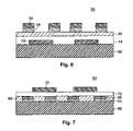
- an array of top gate transistors 60 include a substrate 62 , patterned source, drain, and/or pixel electrodes 64 for each transistor provided adjacent the substrate 62 , a patterned n+amorphous silicon contact 66 provided adjacent each electrode 64 , a boron doped amorphous silicon layer 68 provided adjacent the contacts 66 and the substrate 62 , a dielectric layer 70 provided adjacent to the boron doped amorphous silicon layer 68 , and a gate electrode 72 for each transistor provided adjacent to the dielectric layer 70 .
- an array of bottom gate transistors 80 is substantially similar to the transistors 50 of FIG. 6 .
- the transistors 80 of FIG. 8 include a passivation layer 82 provided above the exposed regions of the boron doped amorphous silicon layer 56 .
- the passivation layer 82 can be deposited after the patterning of the electrodes 59 .
- the passivation layer 82 can consist of silicon nitride.
- a light blocking layer is incorporated into the array of transistors to shield any exposed silicon layer 56 .
- the light blocking layer can be either light absorbing or reflective.
- an array of bottom gate transistors 90 is substantially similar to the array of transistors 80 of FIG. 8 .
- the array of transistors 90 further incorporates a substrate capacitor 92 .
- the substrate capacitor 92 can be formed simply by extending the pixel electrode 94 over the preceding gate line 53 .
- the capacitance is directly proportional to the area of overlap.
- inexpensive displays can be constructed by minimizing the number of patterning steps.
- Such a display can take different forms, including but not limited to: large area displays, displays with low-to-moderate pixel density, or microencapsulated electrophoretic display devices.
- the semiconductor layer 18 , 56 , or 68 is unpatterned.
- the dielectric layer 16 , 54 , or 70 is unpatterned.
- both the semiconductor layer 18 , 56 , or 68 and the dielectric layer 16 , 54 , or 70 layer are unpatterned.
- an electronic display can incorporate an array of transistors as described above.
- an electronic display 100 includes a substrate 101 supporting an electrode 102 , a display medium 106 provided next to the electrode 102 , a plurality of pixel electrodes 104 provided next to the display medium 106 , and a plurality of discrete electronic devices (e.g., transistors) provided next to and in electrical communication with the pixel electrodes 104 supported by a substrate 110 provided next to and in electrical communication with the discrete electronic devices.
- the discrete electronic devices in this embodiment, are transistors.
- the gate electrodes 112 , the gate dielectric layer 100 , the semiconductor layer 118 and the source electrodes 120 of the transistors are shown in this cross-section.
- the substrate 101 can be made of a transparent material.
- the substrate 101 can also be a flexible substrate.
- the substrate 101 can consist of polyester.
- the electrode 102 can be a common electrode.
- the electrode 102 can be a plurality of row electrodes.
- the electrode 102 can consist of a transparent conductive material.
- an indium tin oxide (ITO), polyaniline or polythiophene coating can be provided on an inner surface of the substrate 101 .
- the display medium 106 can include a plurality of microcapsules 124 dispersed in a binder 126 .
- Each microcapsule 124 can include an electro-optical material.
- An electro-optical material refers to a material which displays an optical property in response to an electrical signal. Electro-optical material, for example, can be electrophoretic particles or liquid crystals dispersed in a solvent. An electro-optical material can also be bichromal spheres dispersed in a solvent. Details of electro-optical materials within the microcapsules 124 will be discussed below.
- An important property of the electro-optical material within the microcapsules 124 is that the material is capable of displaying one visible state upon application of an electric field and a different visual state upon application of a different electric field.
- the display medium 106 comprises a particle-based display medium.
- the particle-based display medium comprises an electronic ink.
- An electronic ink is an optoelectronically active material which comprises at least two phases: an electrophoretic contrast medium phase and a coating/binding phase.
- the electrophoretic phase comprises, in some embodiments, a single species of electrophoretic particles dispersed in a clear or dyed medium, or more than one species of electrophoretic particles having distinct physical and electrical characteristics dispersed in a clear or dyed medium.
- the electrophoretic phase is encapsulated, that is, there is a capsule wall phase between the two phases.
- the coating/binding phase includes, in one embodiment, a polymer matrix that surrounds the electrophoretic phase.
- the polymer in the polymeric binder is capable of being dried, crosslinked, or otherwise cured as in traditional inks, and therefore a printing process can be used to deposit the electronic ink onto a substrate.
- the optical quality of an electronic ink is quite distinct from other electronic display materials.
- the most notable difference is that the electronic ink provides a high degree of both reflectance and contrast because it is pigment based (as are ordinary printing inks).
- the light scattered from the electronic ink comes from a very thin layer of pigment close to the top of the viewing surface. In this respect it resembles an ordinary, printed image.
- electronic ink is easily viewed from a wide range of viewing angles in the same manner as a printed page, and such ink approximates a Lambertian contrast curve more closely than any other electronic display material. Since electronic ink can be printed, it can be included on the same surface with any other printed material, including traditional inks.
- Electronic ink can be made optically stable in all display configurations, that is, the ink can be set to a persistent optical state. Fabrication of a display by printing an electronic ink is particularly useful in low power applications because of this stability.
- Electronic ink displays are novel in that they can be addressed by DC voltages and draw very little current.
- the conductive leads and electrodes used to deliver the voltage to electronic ink displays can be of relatively high resistivity.
- the ability to use resistive conductors substantially widens the number and type of materials that can be used as conductors in electronic ink displays.
- ITO indium tin oxide
- the use of costly vacuum-sputtered indium tin oxide (ITO) conductors a standard material in liquid crystal devices, is not required.
- the replacement of ITO with other materials can provide benefits in appearance, processing capabilities (printed conductors), flexibility, and durability.
- the printed electrodes are in contact only with a solid binder, not with a fluid layer (like liquid crystals).
- conductive materials which would otherwise dissolve or be degraded by contact with liquid crystals, can be used in an electronic ink application.
- These conductive coatings include conducting or semiconducting colloids, examples of which are indium tin oxide and antimony-doped tin oxide.
- Organic conductors polymeric conductors and molecular organic conductors also may be used.
- Polymers include, but are not limited to, polyaniline and derivatives, polythiophene and derivatives, poly(3,4-ethylenedioxythiophene) (PEDOT) and derivatives, polypyrrole and derivatives, and polyphenylenevinylene (PPV) and derivatives.
- Organic molecular conductors include, but are not limited to, derivatives of naphthalene, phthalocyanine, and pentacene.
- Polymer layers can be made thinner and more transparent than with traditional displays because conductivity requirements are not as stringent.
- the pixel electrodes 104 can be bonded to the display medium 106 through a binder.
- the binder for example, can be a pressure sensitive adhesive.
- the pixel electrodes 104 can be made from any conductive material.
- the pixel electrodes 104 can be transparent or opaque.
- the pixel electrodes 104 can be made from solder paste, copper, copper-clad polyimide, graphite inks, silver inks and other metal containing conductive inks.
- the pixel electrodes 104 can be formed on a substrate 110 and subsequently bonded to the display medium 106 .
- the discrete electronic devices can be non-linear devices such as transistor for addressing the pixels of the display.
- the non-linear devices can be diodes.
- the electrodes 112 , 120 can be made of any conductive material, either transparent or opaque.
- the conductive material can be printed, coated, or vacuum sputtered.
- the electrodes 102 , 112 , 120 can also be made using transparent materials such as indium tin oxide and conductive polymers such as polyaniline or polythiophenes.
- the electrodes 102 , 112 , 120 can be made of opaque materials such as solder paste, copper, copper-clad polyimide, graphite inks, silver inks and other metal-containing conductive inks.
- the architecture of the electronic display 100 shown in FIG. 10 is exemplary only and other architectures for an electronic display may also be used in accordance with this invention.
- a particle is any component that is charged or capable of acquiring a charge (i.e., has or is capable of acquiring electrophoretic mobility), and, in some cases, this mobility may be zero or close to zero (i.e., the particles will not move).
- the particles may be neat pigments, dyed (laked) pigments or pigment/polymer composites, or any other component that is charged or capable of acquiring a charge.
- Typical considerations for the electrophoretic particle are its optical properties, electrical properties, and surface chemistry.
- the particles may be organic or inorganic compounds, and they may either absorb light or scatter light.
- the particles for use in the invention may further include scattering pigments, absorbing pigments and luminescent particles.
- the particles may be retroreflective, such as corner cubes, or they may be electroluminescent, such as zinc sulfide particles, which emit light when excited by an AC field, or they may be photoluminescent.
- the particles may be surface treated so as to improve charging or interaction with a charging agent, or to improve dispersibility.
- a preferred particle for use in electrophoretic displays of the invention is Titania.
- the titania particles may be coated with a metal oxide, such as aluminum oxide or silicon oxide, for example.
- the titania particles may have one, two, or more layers of metal-oxide coating.
- a titania particle for use in electrophoretic displays of the invention may have a coating of aluminum oxide and a coating of silicon oxide. The coatings may be added to the particle in any order.
- the electrophoretic particle is usually a pigment, a polymer, a laked pigment, or some combination of the above.
- a neat pigment can be any pigment, and, usually for a light colored particle, pigments such as, for example, rutile (titania), anatase (titania), barium sulfate, kaolin, or zinc oxide are useful. Some typical particles have high refractive indices, high scattering coefficients, and low absorption coefficients. Other particles are absorptive, such as carbon black or colored pigments used in paints and inks. The pigment should also be insoluble in the suspending fluid. Yellow pigments such as diarylide yellow, hansa yellow, and benzidin yellow have also found use in similar displays. Any other reflective material can be employed for a light colored particle, including non-pigment materials, such as metallic particles.
- Useful neat pigments include, but are not limited to, PbCrO 4 , Cyan blue GT 55-3295 (American Cyanamid Company, Wayne, N.J.), Cibacron Black BG (Ciba Company, Inc., Newport, Del.), Cibacron Turquoise Blue G (Ciba), Cibalon Black BGL (Ciba), Orasol Black BRG (Ciba), Orasol Black RBL (Ciba), Acetamine Blac, CBS (E.I. du Pont de Nemours and Company, Inc., Wilmington, Del.), Crocein Scarlet N Ex (du Pont) (27290), Fiber Black VF (DuPont) (30235), Luxol Fast Black L (DuPont) (Solv.
- Particles may also include laked, or dyed, pigments.
- Laked pigments are particles that have a dye precipitated on them or which are stained.
- Lakes are metal salts of readily soluble anionic dyes. These are dyes of azo, triphenylmethane or anthraquinone structure containing one or more sulphonic or carboxylic acid groupings. They are usually precipitated by a calcium, barium or aluminum salt onto a substrate. Typical examples are peacock blue lake (CI Pigment Blue 24) and Persian orange (lake of CI Acid Orange 7), Black M Toner (GAF) (a mixture of carbon black and black dye precipitated on a lake).
- CI Pigment Blue 24 and Persian orange (lake of CI Acid Orange 7)
- GAF Black M Toner
- a dark particle of the dyed type may be constructed from any light absorbing material, such as carbon black, or inorganic black materials.
- the dark material may also be selectively absorbing.
- a dark green pigment may be used.
- Black particles may also be formed by staining latices with metal oxides, such latex copolymers consisting of any of butadiene, styrene, isoprene, methacrylic acid, methyl methacrylate, acrylonitrile, vinyl chloride, acrylic acid, sodium styrene sulfonate, vinyl acetate, chlorostyrene, dimethylaminopropylmethacrylamide, isocyanoethyl methacrylate and N-(isobutoxymethacrylamide), and optionally including conjugated diene compounds such as diacrylate, triacrylate, dimethylacrylate and trimethacrylate.
- Black particles may also be formed by a dispersion polymerization technique.
- the pigments and polymers may form multiple domains within the electrophoretic particle, or be aggregates of smaller pigment/polymer combined particles.
- a central pigment core may be surrounded by a polymer shell.
- the pigment, polymer, or both can contain a dye.
- the optical purpose of the particle may be to scatter light, absorb light, or both. Useful sizes may range from 1 nm up to about 100 ⁇ m, as long as the particles are smaller than the bounding capsule.
- the density of the electrophoretic particle may be substantially matched to that of the suspending (i.e., electrophoretic) fluid.
- a suspending fluid has a density that is “substantially matched” to the density of the particle if the difference in their respective densities is between about zero and about two g/ml. This difference is preferably between about zero and about 0.5 g/ml.
- Useful polymers for the particles include, but are not limited to: polystyrene, polyethylene, polypropylene, phenolic resins, Du Pont Elvax resins (ethylene-vinyl acetate copolymers), polyesters, polyacrylates, polymethacrylates, ethylene acrylic acid or methacrylic acid copolymers (Nucrel Resins—DuPont, Primacor Resins-Dow Chemical), acrylic copolymers and terpolymers (Elvacite Resins, DuPont) and PMMA.
- Useful materials for homopolymer/pigment phase separation in high shear melt include, but are not limited to, polyethylene, polypropylene, polymethylmethacrylate, polyisobutylmethacrylate, polystyrene, polybutadiene, polyisoprene, polyisobutylene, polylauryl methacrylate, polystearyl methacrylate, polyisobornyl methacrylate, poly-t-butyl methacrylate, polyethyl methacrylate, polymethyl acrylate, polyethyl acrylate, polyacrylonitrile, and copolymers of two or more of these materials.
- Some useful pigment/polymer complexes that are commercially available include, but are not limited to, Process Magenta PM 1776 (Magruder Color Company, Inc., Elizabeth, N.J.), Methyl Violet PMA VM6223 (Magruder Color Company, Inc., Elizabeth, N.J.), and Naphthol FGR RF6257 (Magruder Color Company, Inc., Elizabeth, N.J.).
- the pigment-polymer composite may be formed by a physical process, (e.g., attrition or ball milling), a chemical process (e.g., microencapsulation or dispersion polymerization), or any other process known in the art of particle production. From the following non-limiting examples, it may be seen that the processes and materials for both the fabrication of particles and the charging thereof are generally derived from the art of liquid toner, or liquid immersion development. Thus any of the known processes from liquid development are particularly, but not exclusively, relevant.
- liquid toners and encapsulated electrophoretic inks are similar, in that the pigment or dye must be easily incorporated therein, either by a physical, chemical, or physicochemical process, may aid in the colloidal stability, and may contain charging sites or may be able to incorporate materials which contain charging sites.
- One general requirement from the liquid toner industry that is not shared by encapsulated electrophoretic inks is that the toner must be capable of “fixing” the image, i.e., heat fusing together to create a uniform film after the deposition of the toner particles.
- Typical manufacturing techniques for particles are drawn from the liquid toner and other arts and include ball milling, attrition, jet milling, etc.
- the process will be illustrated for the case of a pigmented polymeric particle.
- the pigment is compounded in the polymer, usually in some kind of high shear mechanism such as a screw extruder.
- the composite material is then (wet or dry) ground to a starting size of around 10 ⁇ m. It is then dispersed in a carrier liquid, for example ISOPAR® (Exxon, Houston, Tex.), optionally with some charge control agent(s), and milled under high shear for several hours down to a final particle size and/or size distribution.
- a carrier liquid for example ISOPAR® (Exxon, Houston, Tex.), optionally with some charge control agent(s), and milled under high shear for several hours down to a final particle size and/or size distribution.
- Another manufacturing technique for particles drawn from the liquid toner field is to add the polymer, pigment, and suspending fluid to a media mill.
- the mill is started and simultaneously heated to temperature at which the polymer swells substantially with the solvent. This temperature is typically near 100° C. In this state, the pigment is easily encapsulated into the swollen polymer.
- the mill is gradually cooled back to ambient temperature while stirring. The milling may be continued for some time to achieve a small enough particle size, typically a few microns in diameter.
- the charging agents may be added at this time.
- more suspending fluid may be added.
- Chemical processes such as dispersion polymerization, mini- or micro-emulsion polymerization, suspension polymerization precipitation, phase separation, solvent evaporation, in situ polymerization, seeded emulsion polymerization, or any process which falls under the general category of microencapsulation may be used.
- a typical process of this type is a phase separation process wherein a dissolved polymeric material is precipitated out of solution onto a dispersed pigment surface through solvent dilution, evaporation, or a thermal change.
- Other processes include chemical means for staining polymeric latices, for example with metal oxides or dyes.
- the suspending fluid containing the particles can be chosen based on properties such as density, refractive index, and solubility.
- a preferred suspending fluid has a low dielectric constant (about 2), high volume resistivity (about 10 ⁇ 15 ohm-cm), low viscosity (less than 5 cst), low toxicity and environmental impact, low water solubility (less than 10 ppm), high specific gravity (greater than 1.5), a high boiling point (greater than 90° C.), and a low refractive index (less than 1.2).
- suspending fluid may be based on concerns of chemical inertness, density matching to the electrophoretic particle, or chemical compatibility with both the electrophoretic particle and bounding capsule.
- the viscosity of the fluid should be low when you want the particles to move.
- the refractive index of the suspending fluid may also be substantially matched to that of the particles.
- the refractive index of a suspending fluid “is substantially matched” to that of a particle if the difference between their respective refractive indices is between about zero and about 0.3, and is preferably between about 0.05 and about 0.2.
- the fluid may be chosen to be a poor solvent for some polymers, which is advantageous for use in the fabrication of microparticles because it increases the range of polymeric materials useful in fabricating particles of polymers and pigments.
- Organic solvents such as halogenated organic solvents, saturated linear or branched hydrocarbons, silicone oils, and low molecular weight halogen-containing polymers are some useful suspending fluids.
- the suspending fluid may comprise a single fluid.
- the fluid will, however, often be a blend of more than one fluid in order to tune its chemical and physical properties.
- the fluid may contain surface modifiers to modify the surface energy or charge of the electrophoretic particle or bounding capsule. Reactants or solvents for the microencapsulation process (oil soluble monomers, for example) can also be contained in the suspending fluid. Charge control agents can also be added to the suspending fluid.
- Useful organic solvents include, but are not limited to, epoxides, such as, for example, decane epoxide and dodecane epoxide; vinyl ethers, such as, for example, cyclohexyl vinyl ether and Decave® (International Flavors & Fragrances, Inc., New York, N.Y.); and aromatic hydrocarbons, such as, for example, toluene and naphthalene.
- Useful halogenated organic solvents include, but are not limited to, tetrafluorodibromoethylene, tetrachloroethylene, trifluorochloroethylene, 1,2,4-trichlorobenzene, carbon tetrachloride.
- Useful hydrocarbons include, but are not limited to, dodecane, tetradecane, the aliphatic hydrocarbons in the Isopar® series (Exxon, Houston, Tex.), Norpar® (series of normal paraffinic liquids), Shell-Sol® (Shell, Houston, Tex.), and Sol-Trol® (Shell), naphtha, and other petroleum solvents. These materials usually have low densities.
- silicone oils include, but are not limited to, octamethyl cyclosiloxane and higher molecular weight cyclic siloxanes, poly (methyl phenyl siloxane), hexamethyldisiloxane, and polydimethylsiloxane. These materials usually have low densities.
- Useful low molecular weight halogen-containing polymers include, but are not limited to, poly(chlorotrifluoroethylene) polymer (Halogenated hydrocarbon Inc., River Edge, N.J.), Galden® (a perfluorinated ether from Ausimont, Morristown, N.J.), or Krytox® from DuPont (Wilmington, Del.).
- the suspending fluid is a poly(chlorotrifluoroethylene) polymer.
- this polymer has a degree of polymerization from about 2 to about 10. Many of the above materials are available in a range of viscosities, densities, and boiling points.
- the fluid must be capable of being formed into small droplets prior to a capsule being formed.
- Processes for forming small droplets include flow-through jets, membranes, nozzles, or orifices, as well as shear-based emulsifying schemes.
- the formation of small drops may be assisted by electrical or sonic fields.
- Surfactants and polymers can be used to aid in the stabilization and emulsification of the droplets in the case of an emulsion type encapsulation.
- a preferred surfactant for use in displays of the invention is sodium dodecylsulfate.
- the suspending fluid can contain an optically absorbing dye.
- This dye must be soluble in the fluid, but will generally be insoluble in the other components of the capsule.
- the dye can be a pure compound, or blends of dyes to achieve a particular color, including black.
- the dyes can be fluorescent, which would produce a display in which the fluorescence properties depend on the position of the particles.
- the dyes can be photoactive, changing to another color or becoming colorless upon irradiation with either visible or ultraviolet light, providing another means for obtaining an optical response. Dyes could also be polymerizable, forming a solid absorbing polymer inside the bounding shell.
- dyes that can be chosen for use in encapsulated electrophoretic display. Properties important here include light fastness, solubility in the suspending liquid, color, and cost. These are generally from the class of azo, anthraquinone, and triphenylmethane type dyes and may be chemically modified so as to increase the solubility in the oil phase and reduce the adsorption by the particle surface.
- Useful azo dyes include, but are not limited to: the Oil Red dyes, and the Sudan Red and Sudan Black series of dyes.
- Useful anthraquinone dyes include, but are not limited to: the Oil Blue dyes, and the Macrolex Blue series of dyes.
- Useful triphenylmethane dyes include, but are not limited to, Michler's hydrol, Malachite Green, Crystal Violet, and Auramine 0 .
- Charge control agents are used to provide good electrophoretic mobility to the electrophoretic particles.
- Stabilizers are used to prevent agglomeration of the electrophoretic particles, as well as prevent the electrophoretic particles from irreversibly depositing onto the capsule wall.
- Either component can be constructed from materials across a wide range of molecular weights (low molecular weight, oligomeric, or polymeric), and may be pure or a mixture.
- suitable charge control agents are generally adapted from the liquid toner art.
- the charge control agent used to modify and/or stabilize the particle surface charge is applied as generally known in the arts of liquid toners, electrophoretic displays, non-aqueous paint dispersions, and engine-oil additives.
- charging species may be added to non-aqueous media in order to increase electrophoretic mobility or increase electrostatic stabilization.
- the materials can improve steric stabilization as well.
- Different theories of charging are postulated, including selective ion adsorption, proton transfer, and contact electrification.
- An optional charge control agent or charge director may be used. These constituents typically consist of low molecular weight surfactants, polymeric agents, or blends of one or more components and serve to stabilize or otherwise modify the sign and/or magnitude of the charge on the electrophoretic particles.
- the charging properties of the pigment itself may be accounted for by taking into account the acidic or basic surface properties of the pigment, or the charging sites may take place on the carrier resin surface (if present), or a combination of the two. Additional pigment properties which may be relevant are the particle size distribution, the chemical composition, and the lightfastness.
- the charge control agent used to modify and/or stabilize the particle surface charge is applied as generally known in the arts of liquid toners, electrophoretic displays, non-aqueous paint dispersions, and engine-oil additives.
- charging species may be added to non-aqueous media in order to increase electrophoretic mobility or increase electrostatic stabilization.
- the materials can improve steric stabilization as well.
- Different theories of charging are postulated, including selective ion adsorption, proton transfer, and contact electrification.
- Charge adjuvants may also be added. These materials increase the effectiveness of the charge control agents or charge directors.
- the charge adjuvant may be a polyhydroxy compound or an aminoalcohol compound, which are preferably soluble in the suspending fluid in an amount of at least 2% by weight.
- polyhydroxy compounds which contain at least two hydroxyl groups include, but are not limited to, ethylene glycol, 2,4,7,9-tetramethyl-decyne-4,7-diol, poly(propylene glycol), pentaethylene glycol, tripropylene glycol, triethylene glycol, glycerol, pentaerythritol, glycerol tris(12 hydroxystearate), propylene glycerol monohydroxystearate, and ethylene glycol monohydroxystrearate.
- the charge adjuvant is preferably present in the suspending fluid in an amount of about 1 to about 100 mg/g of the particle mass, and more preferably about 50 to about 200 mg/g.
- the surface of the particle may also be chemically modified to aid dispersion, to improve surface charge, and to improve the stability of the dispersion, for example.
- Surface modifiers include organic siloxanes, organohalogen silanes and other functional silane coupling agents (Dow Corning® Z-6070, Z-6124, and 3 additive, Midland, Mich.); organic titanates and zirconates (Tyzor® TOT, TBT, and TE Series, DuPont, Wilmington, Del.); hydrophobing agents, such as long chain (C12 to C50) alkyl and alkyl benzene sulphonic acids, fatty amines or diamines and their salts or quarternary derivatives; and amphipathic polymers which can be covalently bonded to the particle surface.
- charging results as an acid-base reaction between some moiety present in the continuous phase and the particle surface.
- useful materials are those which are capable of participating in such a reaction, or any other charging reaction as known in the art.
- charge control agents which are useful include organic sulfates or sulfonates, metal soaps, block or comb copolymers, organic amides, organic zwitterions, and organic phosphates and phosphonates.
- Useful organic sulfates and sulfonates include, but are not limited to, sodium bis(2-ethyl hexyl) sulfosuccinate, calcium dodecyl benzene sulfonate, calcium petroleum sulfonate, neutral or basic barium dinonylnaphthalene sulfonate, neutral or basic calcium dinonylnaphthalene sulfonate, dodecylbenzenesulfonic acid sodium salt, and ammonium lauryl sulphate.
- Useful metal soaps include, but are not limited to, basic or neutral barium petronate, calcium petronate, Co-, Ca-, Cu-, Mn-, Ni-, Zn-, and Fe- salts of naphthenic acid, Ba-, Al-, Zn-, Cu-, Pb-, and Fe- salts of stearic acid, divalent and trivalent metal carboxylates, such as aluminum tristearate, aluminum octoanate, lithium heptanoate, iron stearate, iron distearate, barium stearate, chromium stearate, magnesium octanoate, calcium stearate, iron naphthenate, and zinc naphthenate, Mn- and Zn- heptanoate, and Ba-, Al-, Co-, Mn-, and Zn- octanoate.
- Useful block or comb copolymers include, but are not limited to, AB diblock copolymers of (A) polymers of 2-(N,N)-dimethylaminoethyl methacrylate quaternized with methyl-p-toluenesulfonate and (B) poly-2-ethylhexyl methacrylate, and comb graft copolymers with oil soluble tails of poly (12-hydroxystearic acid) and having a molecular weight of about 1800, pendant on an oil-soluble anchor group of poly (methyl methacrylate-methacrylic acid).
- Useful organic amides include, but are not limited to, polyisobutylene succinimides such as OLOA 1200, and N-vinyl pyrrolidone polymers.
- Useful organic zwitterions include, but are not limited to, lecithin.
- Useful organic phosphates and phosphonates include, but are not limited to, the sodium salts of phosphated mono- and di-glycerides with saturated and unsaturated acid substituents.
- Particle dispersion stabilizers may be added to prevent particle flocculation or attachment to the capsule walls.
- nonaqueous surfactants include, but are not limited to, glycol ethers, acetylenic glycols, alkanolamides, sorbitol derivatives, alkyl amines, quaternary amines, imidazolines, dialkyl oxides, and sulfosuccinates.
- Encapsulation of the internal phase may be accomplished in a number of different ways. Numerous suitable procedures for microencapsulation are detailed in both Microencapsulation, Processes and Applications , (I. E. Vandegaer, ed.), Plenum Press, New York, N.Y. (1974) and Gutcho, Microcapsules and Mircroencapsulation Techniques , Nuyes Data Corp., Park Ridge, N.J. (1976).
- interfacial polymerization interfacial polymerization
- in situ polymerization physical processes, such as coextrusion and other phase separation processes, in-liquid curing, and simple/complex coacervation.
- Useful materials for simple coacervation processes include, but are not limited to, gelatin, polyvinyl alcohol, polyvinyl acetate, and cellulosic derivatives, such as, for example, carboxymethylcellulose.
- Useful materials for complex coacervation processes include, but are not limited to, gelatin, acacia, carageenan, carboxymethylcellulose, hydrolized styrene anhydride copolymers, agar, alginate, casein, albumin, methyl vinyl ether co-maleic anhydride, and cellulose phthalate.
- Useful materials for phase separation processes include, but are not limited to, polystyrene, PMMA, polyethyl methacrylate, polybutyl methacrylate, ethyl cellulose, polyvinyl pyridine, and poly acrylonitrile.
- Useful materials for in situ polymerization processes include, but are not limited to, polyhydroxyamides, with aldehydes, melamine, or urea and formaldehyde; water-soluble oligomers of the condensate of melamine, or urea and formaldehyde; and vinyl monomers, such as, for example, styrene, MMA and acrylonitrile.
- useful materials for interfacial polymerization processes include, but are not limited to, diacyl chlorides, such as, for example, sebacoyl, adipoyl, and di- or poly-amines or alcohols, and isocyanates.
- useful emulsion polymerization materials may include, but are not limited to, styrene, vinyl acetate, acrylic acid, butyl acrylate, t-butyl acrylate, methyl methacrylate, and butyl methacrylate.
- Capsules produced may be dispersed into a curable carrier, resulting in an ink which may be printed or coated on large and arbitrarily shaped or curved surfaces using conventional printing and coating techniques.
- capsule properties include the distribution of capsule radii; electrical, mechanical, diffusion, and optical properties of the capsule wall; and chemical compatibility with the internal phase of the capsule.
- the capsule wall generally has a high electrical resistivity. Although it is possible to use walls with relatively low resistivities, this may limit performance in requiring relatively higher addressing voltages.
- the capsule wall should also be mechanically strong (although if the finished capsule powder is to be dispersed in a curable polymeric binder for coating, mechanical strength is not as critical).
- the capsule wall should generally not be porous. If, however, it is desired to use an encapsulation procedure that produces porous capsules, these can be overcoated in a post-processing step (i.e., a second encapsulation). Moreover, if the capsules are to be dispersed in a curable binder, the binder will serve to close the pores.
- the capsule walls should be optically clear.
- the wall material may, however, be chosen to match the refractive index of the internal phase of the capsule (i.e., the suspending fluid) or a binder in which the capsules are to be dispersed. For some applications (e.g., interposition between two fixed electrodes), monodispersed capsule radii are desirable.
- An encapsulation procedure involves a polymerization between urea and formaldehyde in an aqueous phase of an oil/water emulsion in the presence of a negatively charged, carboxyl-substituted, linear hydrocarbon polyelectrolyte material.
- the resulting capsule wall is a urea/formaldehyde copolymer, which discretely encloses the internal phase.
- the capsule is clear, mechanically strong, and has good resistivity properties.
- the related technique of in situ polymerization utilizes an oil/water emulsion, which is formed by dispersing the electrophoretic composition (i.e., the dielectric liquid containing a suspension of the pigment particles) in an aqueous environment.
- the monomers polymerize to form a polymer with higher affinity for the internal phase than for the aqueous phase, thus condensing around the emulsified oily droplets.
- urea and formaldehyde condense in the presence of poly(acrylic acid) (See, e.g., U.S. Pat. No. 4,001,140).
- any of a variety of cross-linking agents borne in aqueous solution is deposited around microscopic oil droplets.
- Such cross-linking agents include aldehydes, especially formaldehyde, glyoxal, or glutaraldehyde; alum; zirconium salts; and poly isocyanates.
- the coacervation approach also utilizes an oil/water emulsion.
- One or more colloids are coacervated (i.e., agglomerated) out of the aqueous phase and deposited as shells around the oily droplets through control of temperature, pH and/or relative concentrations, thereby creating the microcapsule.
- Materials suitable for coacervation include gelatins and gum arabic.
- the interfacial polymerization approach relies on the presence of an oil-soluble monomer in the electrophoretic composition, which once again is present as an emulsion in an aqueous phase.
- the monomers in the minute hydrophobic droplets react with a monomer introduced into the aqueous phase, polymerizing at the interface between the droplets and the surrounding aqueous medium and forming shells around the droplets.
- the resulting walls are relatively thin and may be permeable, this process does not require the elevated temperatures characteristic of some other processes, and therefore affords greater flexibility in terms of choosing the dielectric liquid.
- Coating aids can be used to improve the uniformity and quality of the coated or printed electrophoretic ink material.
- Wetting agents are typically added to adjust the interfacial tension at the coating/substrate interface and to adjust the liquid/air surface tension.
- Wetting agents include, but are not limited to, anionic and cationic surfactants, and nonionic species, such as silicone or fluoropolymer based materials.
- Dispersing agents may be used to modify the interfacial tension between the capsules and binder, providing control over flocculation and particle settling.
- Surface tension modifiers can be added to adjust the air/ink interfacial tension.
- Polysiloxanes are typically used in such an application to improve surface leveling while minimizing other defects within the coating.
- Surface tension modifiers include, but are not limited to, fluorinated surfactants, such as, for example, the Zonyl® series from DuPont (Wilmington, Del.), the Fluorod® series from 3M (St. Paul, Minn.), and the fluoroakyl series from Autochem (Glen Rock, N.J.); siloxanes, such as, for example, Silwet® from Union Carbide (Danbury, Conn.); and polyethoxy and polypropoxy alcohols.
- fluorinated surfactants such as, for example, the Zonyl® series from DuPont (Wilmington, Del.), the Fluorod® series from 3M (St. Paul, Minn.), and the fluoroakyl series from Autochem (Glen Rock, N.J
- Antifoams such as silicone and silicone-free polymeric materials, may be added to enhance the movement of air from within the ink to the surface and to facilitate the rupture of bubbles at the coating surface.
- Other useful antifoams include, but are not limited to, glyceryl esters, polyhydric alcohols, compounded antifoams, such as oil solutions of alkyl benzenes, natural fats, fatty acids, and metallic soaps, and silicone antifoaming agents made from the combination of dimethyl siloxane polymers and silica.
- Stabilizers such as uv-absorbers and antioxidants may also be added to improve the lifetime of the ink.
- Stabilizers UV-absorbers, antioxidants
- other additives which could prove useful in practical materials.
- the binder is used as a non-conducting, adhesive medium supporting and protecting the capsules, as well as binding the electrode materials to the capsule dispersion. Binders are available in many forms and chemical types. Among these are water-soluble polymers, water-borne polymers, oil-soluble polymers, thermoset and thermoplastic polymers, and radiation-cured polymers.
- water-soluble polymers are the various polysaccharides, the polyvinyl alcohols, N-methylpyrrolidone, N-vinylpyrrollidone, the various Carbowax® species (Union Carbide, Danbury, Conn.), and poly-2-hydroxyethylacrylate.
- the water-dispersed or water-borne systems are generally latex compositions, typified by the Neorez® and Neocryl® resins (Zeneca Resins, Wilmington, Mass.), Acrysol® (Rohm and Haas, Philadelphia, Pa.), Bayhydrol® (Bayer, Pittsburgh, Pa.), and the Cytec Industries (West Paterson, N.J.) HP line.
- Neorez® and Neocryl® resins Zeneca Resins, Wilmington, Mass.
- Acrysol® Rohm and Haas, Philadelphia, Pa.
- Bayhydrol® Bayhydrol®
- Cytec Industries West Paterson, N.J. HP line.
- a typical application of a water-borne resin and aqueous capsules follows. A volume of particles is centrifuged at low speed to separate excess water. After a given centrifugation process, for example 10 minutes at 60 ⁇ G, the capsules are found at the bottom of the centrifuge tube, while the water portion is at the top. The water portion is carefully removed (by decanting or pipetting). The mass of the remaining capsules is measured, and a mass of resin is added such that the mass of resin is between one eighth and one tenth of the weight of the capsules. This mixture is gently mixed on an oscillating mixer for approximately one half hour. After about one half hour, the mixture is ready to be coated onto the appropriate substrate.
- thermoset systems are exemplified by the family of epoxies. These binary systems can vary greatly in viscosity, and the reactivity of the pair determines the “pot life” of the mixture. If the pot life is long enough to allow a coating operation, capsules may be coated in an ordered arrangement in a coating process prior to the resin curing and hardening.
- Thermoplastic polymers which are often polyesters, are molten at high temperatures.
- a typical application of this type of product is hot-melt glue.
- a dispersion of heat-resistant capsules could be coated in such a medium. The solidification process begins during cooling, and the final hardness, clarity and flexibility are affected by the branching and molecular weight of the polymer.
- Oil or solvent-soluble polymers are often similar in composition to the water-borne system, with the obvious exception of the water itself.
- the latitude in formulation for solvent systems is enormous, limited only by solvent choices and polymer solubility.
- Of considerable concern in solvent-based systems is the viability of the capsule itself—the integrity of the capsule wall cannot be compromised in any way by the solvent.
- Radiation cure resins are generally found among the solvent-based systems. Capsules may be dispersed in such a medium and coated, and the resin may then be cured by a timed exposure to a threshold level of ultraviolet radiation, either long or short wavelength. As in all cases of curing polymer resins, final properties are determined by the branching and molecular weights of the monomers, oligomers and crosslinkers.
- water-reducible monomers and oligomers are, however, marketed. In the strictest sense, they are not water soluble, but water is an acceptable diluent at low concentrations and can be dispersed relatively easily in the mixture. Under these circumstances, water is used to reduce the viscosity (initially from thousands to hundreds of thousands centipoise).
- Water-based capsules such as those made from a protein or polysaccharide material, for example, could be dispersed in such a medium and coated, provided the viscosity could be sufficiently lowered. Curing in such systems is generally by ultraviolet radiation.
- FIG. 11 a shows a diagrammatic cross-section of an electrophoretic display 130 constructed using electronic ink.
- the binder 132 includes at least one capsule 134 , which is filled with a plurality of particles 136 and a dyed suspending fluid 138 .
- the particles 136 are titania particles.
- FIG. 11 b shows a cross-section of another electrophoretic display 140 constructed using electronic ink.
- This display comprises a first set of particles 142 and a second set of particles 144 in a capsule 141 .
- the first set of particles 142 and the second set of particles 144 have contrasting optical properties.
- the first set of particles 142 and the second set of particles 144 can have differing electrophoretic mobilities.
- the first set of particles 142 and the second set of particles 144 can have contrasting colors.
- the first set of particles 142 can be white, while the second set of particles 144 can be black.
- the capsule 141 further includes a substantially clear fluid.
- the capsule 141 has electrodes 146 and 146 ′ disposed adjacent it.
- the electrodes 146 , 146 ′ are connected to a source of voltage 148 , which may provide an electric field to the capsule 141 .
- a source of voltage 148 which may provide an electric field to the capsule 141 .
- the first set of particles 142 move toward electrode 146 ′, while the second set of particles 144 move toward electrode 146 .
- the first set of particles 142 move rapidly toward electrode 146 ′, while the second set of particles 144 move only slowly or not at all towards electrode 146 , so that the first set of particles packs preferentially at the microcapsule surface adjacent to electrode 146 ′.
- FIG. 11 c shows a diagrammatic cross-section of a suspended particle display 150 .
- the suspended particle display 150 includes needle-like particles 152 in a transparent fluid 154 .
- the particles 152 change their orientation upon application of an AC field across the electrodes 156 , 156 ′. When the AC field is applied, the particles 152 are oriented perpendicular with respect to the display surface and the display appears transparent. When the AC field is removed, the particles 152 are randomly oriented and the display 150 appears opaque.
- FIGS. 9 a – 9 c are exemplary only, and other electrophoretic displays can be used in accordance with the present invention.
- the display medium 106 can comprise a plurality of bichromal spheres shown in FIG. 1 d .
- a bichromal sphere 160 typically comprises a positively charged hemisphere 162 of a first color and a negatively charged hemisphere 164 of a second color in a liquid medium 166 .
- the sphere 160 rotates and displays the color of one of the two hemispheres 162 , 164 .
- an array of transistors with reduced cross-talk is prepared by increasing the resistivity of the semiconductor layer.
- the semiconductor layer is an amorphous silicon that is slightly n-type
- the semiconductor can be lightly doped with boron or an equivalent p-type dopant to increase the resistivity of the semiconductor layer. If the semiconductor layer is doped with too much boron, the semiconductor layer will become p-type and the resistivity will decrease.
- the boron doping can be adjusted to provide the minimum required “on” current for the transistor to drive a pixel of a display, while concurrently maintaining sufficient isolation between neighboring elements or signals.
- the spacing between neighboring source and drain electrodes of the transistors and the metal signal lines must be sufficiently large to suppress charge leakage through the underlying semiconductor layer in this embodiment.
- This minimum spacing can be derived via a resistance calculation if the leakage current, electrode potential, semiconductor conductivity and thickness of various materials are known.
- an array of active or passive elements can be prepared in accordance with the present invention.
- the array of elements can be used in devices other than displays.
Abstract
Description
where
R 1 +R 2 >>NR d
and
R TFT >>NR d
The data line also should not charge up an adjacent pixel while the select line is off (row unselected). This demand can be translated as:
R TFT >>R p
and
R 2 >>R p
-
- where Rp is the resistance through the pixel.
I leak T f <C p δV p
where Ileak is the leakage current from the data line to the pixel electrode through the unpatterned semiconductor layer, Tf is the frame time, and Cp is the total capacitance of the pixel. δVp is the maximum tolerance for leakage-induced voltage shifts on the pixel electrode. This value depends on how voltage shifts affect the optical state of the pixel and the tolerance defined by the display parameters.
I leak =σwh(V p −V d)/L ms
where σ is the conductivity of the semiconductor material, w is the width of the leakage path, h is the thickness of the underlying semiconductor material, and Vd is the voltage of the data line.
L ms >σwh(V p −V d)T f /C pix δV p.
The above discussion applies to embodiments with a single leakage source. If there are multiple leakage sources, Ileak, will include leakage currents from each leakage source and the minimum spacing Lms for each leakage path must be derived accordingly.
| Max. | Min. | |||||||
| On/Off | Threshold | Drain | Drain | Storage | ||||
| Sample | WL | Ratio | Mobility | Voltage | Gm | Current | Current | capacitance |
| Patterned | 200/20 | 1 × 10⁸ | .55 cm2/Vs | 5.0 V | 18.9 nA/ |
10 μA | 0.1 pA | 19.1 |
| Unpatterned | ||||||||
| 160/20 | 3.3 × 10⁵ | .43 cm2/Vs | 5.0 V | 23.4 nA/ |
20 μA | 60 pA | 18.4 pF | |
Claims (15)
Priority Applications (1)
| Application Number | Priority Date | Filing Date | Title |
|---|---|---|---|
| US09/565,413 US7030412B1 (en) | 1999-05-05 | 2000-05-05 | Minimally-patterned semiconductor devices for display applications |
Applications Claiming Priority (2)
| Application Number | Priority Date | Filing Date | Title |
|---|---|---|---|
| US13264299P | 1999-05-05 | 1999-05-05 | |
| US09/565,413 US7030412B1 (en) | 1999-05-05 | 2000-05-05 | Minimally-patterned semiconductor devices for display applications |
Publications (1)
| Publication Number | Publication Date |
|---|---|
| US7030412B1 true US7030412B1 (en) | 2006-04-18 |
Family
ID=36147385
Family Applications (1)
| Application Number | Title | Priority Date | Filing Date |
|---|---|---|---|
| US09/565,413 Expired - Fee Related US7030412B1 (en) | 1999-05-05 | 2000-05-05 | Minimally-patterned semiconductor devices for display applications |
Country Status (1)
| Country | Link |
|---|---|
| US (1) | US7030412B1 (en) |
Cited By (146)
| Publication number | Priority date | Publication date | Assignee | Title |
|---|---|---|---|---|
| US20040179146A1 (en) * | 2003-01-17 | 2004-09-16 | Nilsson Boo Jorgen Lars | Display employing organic material |
| US20040263948A1 (en) * | 2003-04-22 | 2004-12-30 | Yong-Uk Lee | Electrophorectic display device |
| US20050122565A1 (en) * | 2003-11-05 | 2005-06-09 | E Ink Corporation | Electro-optic displays, and materials for use therein |
| US20050190137A1 (en) * | 2004-02-27 | 2005-09-01 | E Ink Corporation | Backplanes for electro-optic displays |
| US20050212747A1 (en) * | 2004-03-26 | 2005-09-29 | E Ink Corporation | Methods for driving bistable electro-optic displays |
| US20050253777A1 (en) * | 2004-05-12 | 2005-11-17 | E Ink Corporation | Tiled displays and methods for driving same |
| US20050280626A1 (en) * | 2001-11-20 | 2005-12-22 | E Ink Corporation | Methods and apparatus for driving electro-optic displays |
| US20060197737A1 (en) * | 2001-03-13 | 2006-09-07 | E Ink Corporation | Apparatus for displaying drawings |
| US20060209388A1 (en) * | 2005-01-26 | 2006-09-21 | E Ink Corporation | Electrophoretic displays using gaseous fluids |
| US20070035808A1 (en) * | 2001-07-09 | 2007-02-15 | E Ink Corporation | Electro-optic display and materials for use therein |
| US20070051953A1 (en) * | 2005-02-21 | 2007-03-08 | Ludger Marwitz | Active matrix structure for a display device and method for its manufacture |
| US20070091417A1 (en) * | 2005-10-25 | 2007-04-26 | E Ink Corporation | Electrophoretic media and displays with improved binder |
| US20070153361A1 (en) * | 2002-06-10 | 2007-07-05 | E Ink Corporation | Components and testing methods for use in the production of electro-optic displays |
| US20070211331A1 (en) * | 2006-03-08 | 2007-09-13 | E Ink Corporation | Electro-optic displays, and materials and methods for production thereof |
| US20070247697A1 (en) * | 2003-11-05 | 2007-10-25 | E Ink Corporation | Electro-optic displays, and materials for use therein |
| US20070286975A1 (en) * | 2003-11-05 | 2007-12-13 | E Ink Corporation | Electro-optic displays, and materials for use therein |
| US20070295242A1 (en) * | 2006-05-16 | 2007-12-27 | Shim Anne K | Low viscosity, high particulate loading dispersions |
| US20080013155A1 (en) * | 2006-07-11 | 2008-01-17 | E Ink Corporation | Electrophoretic medium and display with improved image stability |
| US20080013156A1 (en) * | 2006-07-13 | 2008-01-17 | E Ink Corporation | Particles for use in electrophoretic displays |
| US20080024429A1 (en) * | 2006-07-25 | 2008-01-31 | E Ink Corporation | Electrophoretic displays using gaseous fluids |
| US20080023332A1 (en) * | 2003-03-25 | 2008-01-31 | E Ink Corporation | Processes for the production of electrophoretic displays |
| US20080024482A1 (en) * | 2002-06-13 | 2008-01-31 | E Ink Corporation | Methods for driving electro-optic displays |
| US20080043318A1 (en) * | 2005-10-18 | 2008-02-21 | E Ink Corporation | Color electro-optic displays, and processes for the production thereof |
| US20080048969A1 (en) * | 2003-06-30 | 2008-02-28 | E Ink Corporation | Methods for driving electrophoretic displays |
| US20080074730A1 (en) * | 2006-09-22 | 2008-03-27 | E Ink Corporation | Electro-optic display and materials for use therein |
| US20080088542A1 (en) * | 2004-05-21 | 2008-04-17 | Osram Opto Semiconductors Gmbh | Determining leakage in matrix-structured electronic devices |
| US20080129667A1 (en) * | 2004-03-31 | 2008-06-05 | E Ink Corporation | Methods for driving electro-optic displays |
| US20080137176A1 (en) * | 2006-12-07 | 2008-06-12 | E Ink Corporation | Components and methods for use in electro-optic displays |
| US20080169464A1 (en) * | 2006-11-07 | 2008-07-17 | Diode Solutions, Inc. | Metal-insulator- metal (MIM) devices and their methods of fabrication |
| US20080174853A1 (en) * | 2007-01-22 | 2008-07-24 | E Ink Corporation | Multi-layer sheet for use in electro-optic displays |
| US20080218839A1 (en) * | 2003-11-05 | 2008-09-11 | E Ink Corporation | Electro-optic displays, and materials for use therein |
| US20080254272A1 (en) * | 2007-01-22 | 2008-10-16 | E Ink Corporation | Multi-layer sheet for use in electro-optic displays |
| US20080266646A1 (en) * | 1995-07-20 | 2008-10-30 | E Ink Corporation | Electrophoretic displays with controlled amounts of pigment |
| US20080266245A1 (en) * | 2001-04-02 | 2008-10-30 | E Ink Corporation | Electrophoretic displays with controlled amounts of pigment |
| US20080291129A1 (en) * | 2007-05-21 | 2008-11-27 | E Ink Corporation | Methods for driving video electro-optic displays |
| US20080309350A1 (en) * | 2006-03-08 | 2008-12-18 | E Ink Corporation | Electro-optic displays, and materials and methods for production thereof |
| US20080316582A1 (en) * | 2006-03-08 | 2008-12-25 | E Ink Corporation | Electro-optic displays, and materials and methods for production thereof |
| US20090000729A1 (en) * | 2007-06-29 | 2009-01-01 | E Ink Corporation | Electro-optic displays, and materials and methods for production thereof |
| US20090004442A1 (en) * | 2007-06-28 | 2009-01-01 | E Ink Corporation | Processes for the production of electro-optic displays, and color filters for use therein |
| US20090109519A1 (en) * | 2007-03-06 | 2009-04-30 | E Ink Corporation | Materials for use in electrophoretic displays |
| US20090168067A1 (en) * | 2002-06-10 | 2009-07-02 | E Ink Corporation | Components and methods for use in electro-optic displays |
| US20090231661A1 (en) * | 2005-06-23 | 2009-09-17 | E Ink Corporation | Edge seals for, and processes for assembly of, electro-optic displays |
| US7649674B2 (en) | 2002-06-10 | 2010-01-19 | E Ink Corporation | Electro-optic display with edge seal |
| US7679814B2 (en) | 2001-04-02 | 2010-03-16 | E Ink Corporation | Materials for use in electrophoretic displays |
| US20100068839A1 (en) * | 2007-05-31 | 2010-03-18 | Nthdegree Technologies Worldwide Inc. | Method of Manufacturing a Light Emitting, Photovoltaic or Other Electronic Apparatus and System |
| US20100165446A1 (en) * | 2002-06-10 | 2010-07-01 | E Ink Corporation | Components and methods for use in electro-optic displays |
| US20100176381A1 (en) * | 2007-01-10 | 2010-07-15 | Sony Corporation | Semiconductor device and display device |
| US20100225995A1 (en) * | 2009-03-03 | 2010-09-09 | E Ink Corporation | Electro-optic displays, and color filters for use therein |
| US20100265239A1 (en) * | 2002-04-24 | 2010-10-21 | E Ink Corporation | Processes for forming backplanes for electro-optic displays |
| US20100289736A1 (en) * | 2009-02-09 | 2010-11-18 | E Ink Corporation | Electrophoretic particles, and processes for the production thereof |
| US7839564B2 (en) | 2002-09-03 | 2010-11-23 | E Ink Corporation | Components and methods for use in electro-optic displays |
| US7848007B2 (en) | 1995-07-20 | 2010-12-07 | E Ink Corporation | Electrophoretic medium and process for the production thereof |
| US7898042B2 (en) | 2006-11-07 | 2011-03-01 | Cbrite Inc. | Two-terminal switching devices and their methods of fabrication |
| US7952790B2 (en) | 2006-03-22 | 2011-05-31 | E Ink Corporation | Electro-optic media produced using ink jet printing |
| US20110129405A1 (en) * | 2006-04-04 | 2011-06-02 | 6N Silicon Inc. | Method for purifying silicon |
| US7986450B2 (en) | 2006-09-22 | 2011-07-26 | E Ink Corporation | Electro-optic display and materials for use therein |
| US7999787B2 (en) | 1995-07-20 | 2011-08-16 | E Ink Corporation | Methods for driving electrophoretic displays using dielectrophoretic forces |
| US8040594B2 (en) | 1997-08-28 | 2011-10-18 | E Ink Corporation | Multi-color electrophoretic displays |
| US8054526B2 (en) | 2008-03-21 | 2011-11-08 | E Ink Corporation | Electro-optic displays, and color filters for use therein |
| US8115729B2 (en) | 1999-05-03 | 2012-02-14 | E Ink Corporation | Electrophoretic display element with filler particles |
| US8125501B2 (en) | 2001-11-20 | 2012-02-28 | E Ink Corporation | Voltage modulated driver circuits for electro-optic displays |
| US8133768B2 (en) | 2007-05-31 | 2012-03-13 | Nthdegree Technologies Worldwide Inc | Method of manufacturing a light emitting, photovoltaic or other electronic apparatus and system |
| US8139050B2 (en) | 1995-07-20 | 2012-03-20 | E Ink Corporation | Addressing schemes for electronic displays |
| US8183772B2 (en) | 2004-12-27 | 2012-05-22 | Nthdegree Technologies Worldwide Inc | Static and addressable emissive displays |
| US8305341B2 (en) | 1995-07-20 | 2012-11-06 | E Ink Corporation | Dielectrophoretic displays |
| US8314784B2 (en) | 2008-04-11 | 2012-11-20 | E Ink Corporation | Methods for driving electro-optic displays |
| US8319759B2 (en) | 2003-10-08 | 2012-11-27 | E Ink Corporation | Electrowetting displays |
| US8363299B2 (en) | 2002-06-10 | 2013-01-29 | E Ink Corporation | Electro-optic displays, and processes for the production thereof |
| EP2555182A1 (en) | 2007-02-02 | 2013-02-06 | E Ink Corporation | Electrophoretic displays having transparent electrode and conductor connected thereto |
| US8415879B2 (en) | 2007-05-31 | 2013-04-09 | Nthdegree Technologies Worldwide Inc | Diode for a printable composition |
| US8413359B2 (en) | 2008-05-13 | 2013-04-09 | Nthdegree Technologies Worldwide Inc | Illuminating display systems |
| US8446664B2 (en) | 2010-04-02 | 2013-05-21 | E Ink Corporation | Electrophoretic media, and materials for use therein |
| WO2013074167A1 (en) | 2011-11-18 | 2013-05-23 | Avon Products, Inc. | Use of electrophoretic microcapsules in a cosmetic composition |
| US8593396B2 (en) | 2001-11-20 | 2013-11-26 | E Ink Corporation | Methods and apparatus for driving electro-optic displays |
| US8610988B2 (en) | 2006-03-09 | 2013-12-17 | E Ink Corporation | Electro-optic display with edge seal |
| US8654436B1 (en) | 2009-10-30 | 2014-02-18 | E Ink Corporation | Particles for use in electrophoretic displays |
| US8674593B2 (en) | 2007-05-31 | 2014-03-18 | Nthdegree Technologies Worldwide Inc | Diode for a printable composition |
| EP2711770A2 (en) | 2005-10-18 | 2014-03-26 | E Ink Corporation | Components for electro-optic displays |
| US8728223B2 (en) | 2006-05-16 | 2014-05-20 | Cabot Corporation | Low viscosity, high particulate loading dispersions |
| US8739441B2 (en) | 2008-05-13 | 2014-06-03 | Nthdegree Technologies Worldwide Inc | Apparatuses for providing power for illumination of a display object |
| US8754859B2 (en) | 2009-10-28 | 2014-06-17 | E Ink Corporation | Electro-optic displays with touch sensors and/or tactile feedback |
| US8809126B2 (en) | 2007-05-31 | 2014-08-19 | Nthdegree Technologies Worldwide Inc | Printable composition of a liquid or gel suspension of diodes |
| US8846457B2 (en) | 2007-05-31 | 2014-09-30 | Nthdegree Technologies Worldwide Inc | Printable composition of a liquid or gel suspension of diodes |
| US8852467B2 (en) | 2007-05-31 | 2014-10-07 | Nthdegree Technologies Worldwide Inc | Method of manufacturing a printable composition of a liquid or gel suspension of diodes |
| US8877101B2 (en) | 2007-05-31 | 2014-11-04 | Nthdegree Technologies Worldwide Inc | Method of manufacturing a light emitting, power generating or other electronic apparatus |
| US8889216B2 (en) | 2007-05-31 | 2014-11-18 | Nthdegree Technologies Worldwide Inc | Method of manufacturing addressable and static electronic displays |
| US8902153B2 (en) | 2007-08-03 | 2014-12-02 | E Ink Corporation | Electro-optic displays, and processes for their production |
| US9018833B2 (en) | 2007-05-31 | 2015-04-28 | Nthdegree Technologies Worldwide Inc | Apparatus with light emitting or absorbing diodes |
| US9293511B2 (en) | 1998-07-08 | 2016-03-22 | E Ink Corporation | Methods for achieving improved color in microencapsulated electrophoretic devices |
| US9343593B2 (en) | 2007-05-31 | 2016-05-17 | Nthdegree Technologies Worldwide Inc | Printable composition of a liquid or gel suspension of diodes |
| US9412314B2 (en) | 2001-11-20 | 2016-08-09 | E Ink Corporation | Methods for driving electro-optic displays |
| US9419179B2 (en) | 2007-05-31 | 2016-08-16 | Nthdegree Technologies Worldwide Inc | Diode for a printable composition |
| US9425357B2 (en) | 2007-05-31 | 2016-08-23 | Nthdegree Technologies Worldwide Inc. | Diode for a printable composition |
| US9470950B2 (en) | 2002-06-10 | 2016-10-18 | E Ink Corporation | Electro-optic displays, and processes for the production thereof |
| WO2016191673A1 (en) | 2015-05-27 | 2016-12-01 | E Ink Corporation | Methods and circuitry for driving display devices |
| US9529240B2 (en) | 2014-01-17 | 2016-12-27 | E Ink Corporation | Controlled polymeric material conductivity for use in a two-phase electrode layer |
| US9530363B2 (en) | 2001-11-20 | 2016-12-27 | E Ink Corporation | Methods and apparatus for driving electro-optic displays |
| US9534772B2 (en) | 2007-05-31 | 2017-01-03 | Nthdegree Technologies Worldwide Inc | Apparatus with light emitting diodes |
| US9564088B2 (en) | 2001-11-20 | 2017-02-07 | E Ink Corporation | Electro-optic displays with reduced remnant voltage |
| US9620067B2 (en) | 2003-03-31 | 2017-04-11 | E Ink Corporation | Methods for driving electro-optic displays |
| US9664978B2 (en) | 2002-10-16 | 2017-05-30 | E Ink Corporation | Electrophoretic displays |
| US9671635B2 (en) | 2014-02-07 | 2017-06-06 | E Ink Corporation | Electro-optic display backplane structures with drive components and pixel electrodes on opposed surfaces |
| US9715155B1 (en) | 2013-01-10 | 2017-07-25 | E Ink Corporation | Electrode structures for electro-optic displays |
| US9726957B2 (en) | 2013-01-10 | 2017-08-08 | E Ink Corporation | Electro-optic display with controlled electrochemical reactions |
| US9741901B2 (en) | 2006-11-07 | 2017-08-22 | Cbrite Inc. | Two-terminal electronic devices and their methods of fabrication |
| US9835925B1 (en) | 2015-01-08 | 2017-12-05 | E Ink Corporation | Electro-optic displays, and processes for the production thereof |
| US9964831B2 (en) | 2007-11-14 | 2018-05-08 | E Ink Corporation | Electro-optic assemblies, and adhesives and binders for use therein |
| US10048564B2 (en) | 2003-11-05 | 2018-08-14 | E Ink Corporation | Electro-optic displays, and materials for use therein |
| KR101891719B1 (en) | 2011-05-24 | 2018-08-24 | 엘지디스플레이 주식회사 | Array substrate and method of fabricating the same |
| US10175550B2 (en) | 2014-11-07 | 2019-01-08 | E Ink Corporation | Applications of electro-optic displays |
| US10190743B2 (en) | 2012-04-20 | 2019-01-29 | E Ink Corporation | Illumination systems for reflective displays |
| WO2019089042A1 (en) | 2017-11-03 | 2019-05-09 | E Ink Corporation | Processes for producing electro-optic displays |
| US10317767B2 (en) | 2014-02-07 | 2019-06-11 | E Ink Corporation | Electro-optic display backplane structure with drive components and pixel electrodes on opposed surfaces |
| US10319314B2 (en) | 1999-04-30 | 2019-06-11 | E Ink Corporation | Methods for driving electro-optic displays, and apparatus for use therein |
| US10324577B2 (en) | 2017-02-28 | 2019-06-18 | E Ink Corporation | Writeable electrophoretic displays including sensing circuits and styli configured to interact with sensing circuits |
| US10444590B2 (en) | 2002-09-03 | 2019-10-15 | E Ink Corporation | Electro-optic displays |
| US10446585B2 (en) | 2014-03-17 | 2019-10-15 | E Ink Corporation | Multi-layer expanding electrode structures for backplane assemblies |
| US10466565B2 (en) | 2017-03-28 | 2019-11-05 | E Ink Corporation | Porous backplane for electro-optic display |
| US10475396B2 (en) | 2015-02-04 | 2019-11-12 | E Ink Corporation | Electro-optic displays with reduced remnant voltage, and related apparatus and methods |
| US10495941B2 (en) | 2017-05-19 | 2019-12-03 | E Ink Corporation | Foldable electro-optic display including digitization and touch sensing |
| US10527899B2 (en) | 2016-05-31 | 2020-01-07 | E Ink Corporation | Backplanes for electro-optic displays |
| US10573257B2 (en) | 2017-05-30 | 2020-02-25 | E Ink Corporation | Electro-optic displays |
| WO2020060960A1 (en) | 2018-09-17 | 2020-03-26 | E Ink Corporation | Backplanes with hexagonal and triangular electrodes |
| WO2020097462A1 (en) | 2018-11-09 | 2020-05-14 | E Ink Corporation | Electro-optic displays |
| WO2020122917A1 (en) | 2018-12-13 | 2020-06-18 | E Ink Corporation | Illumination systems for reflective displays |
| US10726798B2 (en) | 2003-03-31 | 2020-07-28 | E Ink Corporation | Methods for operating electro-optic displays |
| US10824042B1 (en) | 2017-10-27 | 2020-11-03 | E Ink Corporation | Electro-optic display and composite materials having low thermal sensitivity for use therein |
| CN111952321A (en) * | 2019-05-17 | 2020-11-17 | 元太科技工业股份有限公司 | Display device and thin film transistor array substrate |
| US10882042B2 (en) | 2017-10-18 | 2021-01-05 | E Ink Corporation | Digital microfluidic devices including dual substrates with thin-film transistors and capacitive sensing |
| US11081066B2 (en) | 2018-02-15 | 2021-08-03 | E Ink Corporation | Via placement for slim border electro-optic display backplanes with decreased capacitive coupling between t-wires and pixel electrodes |
| US11099444B2 (en) | 2019-05-17 | 2021-08-24 | E Ink Holdings Inc. | Display device and thin film transistor array substrate |
| US11175561B1 (en) | 2018-04-12 | 2021-11-16 | E Ink Corporation | Electrophoretic display media with network electrodes and methods of making and using the same |
| US11250794B2 (en) | 2004-07-27 | 2022-02-15 | E Ink Corporation | Methods for driving electrophoretic displays using dielectrophoretic forces |
| US11397361B2 (en) | 2015-06-29 | 2022-07-26 | E Ink Corporation | Method for mechanical and electrical connection to display electrodes |
| US11404013B2 (en) | 2017-05-30 | 2022-08-02 | E Ink Corporation | Electro-optic displays with resistors for discharging remnant charges |
| US11467466B2 (en) | 2012-04-20 | 2022-10-11 | E Ink Corporation | Illumination systems for reflective displays |
| US11513415B2 (en) | 2020-06-03 | 2022-11-29 | E Ink Corporation | Foldable electrophoretic display module including non-conductive support plate |
| US11511096B2 (en) | 2018-10-15 | 2022-11-29 | E Ink Corporation | Digital microfluidic delivery device |
| US11521565B2 (en) | 2018-12-28 | 2022-12-06 | E Ink Corporation | Crosstalk reduction for electro-optic displays |
| US11537024B2 (en) | 2018-12-30 | 2022-12-27 | E Ink California, Llc | Electro-optic displays |
| US11733580B2 (en) | 2010-05-21 | 2023-08-22 | E Ink Corporation | Method for driving two layer variable transmission display |
| WO2023164078A1 (en) | 2022-02-25 | 2023-08-31 | E Ink Corporation | Electro-optic displays with edge seal components and methods of making the same |
| WO2023167901A1 (en) | 2022-03-01 | 2023-09-07 | E Ink California, Llc | Temperature compensation in electro-optic displays |
| WO2023211699A1 (en) | 2022-04-27 | 2023-11-02 | E Ink Corporation | Electro-optic display stacks with segmented electrodes and methods of making the same |
| US11892739B2 (en) | 2020-02-07 | 2024-02-06 | E Ink Corporation | Electrophoretic display layer with thin film top electrode |
| US11935495B2 (en) | 2021-08-18 | 2024-03-19 | E Ink Corporation | Methods for driving electro-optic displays |
Citations (101)
| Publication number | Priority date | Publication date | Assignee | Title |
|---|---|---|---|---|
| US3036388A (en) | 1961-10-27 | 1962-05-29 | Clarence R Tate | Magnetic writing materials set |
| US3384488A (en) | 1964-07-23 | 1968-05-21 | Xcrox Corp | Polychromatic photoelectrophoretic imaging composition |
| US3612758A (en) | 1969-10-03 | 1971-10-12 | Xerox Corp | Color display device |
| US3670323A (en) | 1970-12-14 | 1972-06-13 | Zenith Radio Corp | Image-display devices comprising particle light modulators with storage |
| US3767392A (en) | 1970-04-15 | 1973-10-23 | Matsushita Electric Ind Co Ltd | Electrophoretic light image reproduction process |
| US3792308A (en) | 1970-06-08 | 1974-02-12 | Matsushita Electric Ind Co Ltd | Electrophoretic display device of the luminescent type |
| US3806893A (en) | 1971-07-29 | 1974-04-23 | Matsushita Electric Ind Co Ltd | Method of electrically detecting colloidal memory |
| US3850627A (en) | 1971-01-06 | 1974-11-26 | Xerox Corp | Electrophoretic imaging method |
| US3972040A (en) | 1973-08-15 | 1976-07-27 | The Secretary Of State For Defence In Her Britannic Majesty's Government Of The United Kingdom Of Great Britain And Northern Ireland | Display systems |
| US4041481A (en) | 1974-10-05 | 1977-08-09 | Matsushita Electric Industrial Co., Ltd. | Scanning apparatus for an electrophoretic matrix display panel |
| US4045327A (en) | 1974-08-28 | 1977-08-30 | Matsushita Electric Industrial Co., Ltd. | Electrophoretic matrix panel |
| US4068927A (en) | 1976-09-01 | 1978-01-17 | North American Philips Corporation | Electrophoresis display with buried lead lines |
| US4071430A (en) | 1976-12-06 | 1978-01-31 | North American Philips Corporation | Electrophoretic image display having an improved switching time |
| US4088395A (en) | 1976-05-27 | 1978-05-09 | American Cyanamid Company | Paper counter-electrode for electrochromic devices |
| US4123346A (en) | 1976-05-11 | 1978-10-31 | Thomson-Csf | Electrophoretic device |
| US4149149A (en) | 1976-02-20 | 1979-04-10 | Hitachi, Ltd. | Circuit for actuating a display with an improved comparator |
| US4203106A (en) | 1977-11-23 | 1980-05-13 | North American Philips Corporation | X-Y addressable electrophoretic display device with control electrode |
| US4218302A (en) | 1979-08-02 | 1980-08-19 | U.S. Philips Corporation | Electrophoretic display devices |
| US4261653A (en) | 1978-05-26 | 1981-04-14 | The Bendix Corporation | Light valve including dipolar particle construction and method of manufacture |
| US4305807A (en) | 1980-03-13 | 1981-12-15 | Burroughs Corporation | Electrophoretic display device using a liquid crystal as a threshold device |
| US4311361A (en) | 1980-03-13 | 1982-01-19 | Burroughs Corporation | Electrophoretic display using a non-Newtonian fluid as a threshold device |
| US4324456A (en) | 1979-08-02 | 1982-04-13 | U.S. Philips Corporation | Electrophoretic projection display systems |
| US4390403A (en) | 1981-07-24 | 1983-06-28 | Batchelder J Samuel | Method and apparatus for dielectrophoretic manipulation of chemical species |
| US4418346A (en) | 1981-05-20 | 1983-11-29 | Batchelder J Samuel | Method and apparatus for providing a dielectrophoretic display of visual information |
| US4430648A (en) | 1980-01-22 | 1984-02-07 | Citizen Watch Company Limited | Combination matrix array display and memory system |
| US4439507A (en) | 1982-09-21 | 1984-03-27 | Xerox Corporation | Layered photoresponsive imaging device with photogenerating pigments dispersed in a polyhydroxy ether composition |
| US4450440A (en) | 1981-12-24 | 1984-05-22 | U.S. Philips Corporation | Construction of an epid bar graph |
| US4502934A (en) | 1982-06-01 | 1985-03-05 | Thomson-Csf | Electrode comprising an electrochrome polymer film and a display device using such an electrode |
| US4522472A (en) | 1982-02-19 | 1985-06-11 | North American Philips Corporation | Electrophoretic image display with reduced drives and leads |
| US4543306A (en) | 1982-06-01 | 1985-09-24 | Thomson-Csf | Electrochemical device which can be used for energy storage |
| US4598960A (en) | 1985-04-29 | 1986-07-08 | Copytele, Inc. | Methods and apparatus for connecting closely spaced large conductor arrays employing multi-conductor carrier boards |
| US4643528A (en) | 1985-03-18 | 1987-02-17 | Manchester R & D Partnership | Encapsulated liquid crystal and filler material |
| US4648956A (en) | 1984-12-31 | 1987-03-10 | North American Philips Corporation | Electrode configurations for an electrophoretic display device |
| US4655897A (en) | 1984-11-13 | 1987-04-07 | Copytele, Inc. | Electrophoretic display panels and associated methods |
| US4686524A (en) | 1985-11-04 | 1987-08-11 | North American Philips Corporation | Photosensitive electrophoretic displays |
| US4732830A (en) | 1984-11-13 | 1988-03-22 | Copytele, Inc. | Electrophoretic display panels and associated methods |
| US4741604A (en) | 1985-02-01 | 1988-05-03 | Kornfeld Cary D | Electrode arrays for cellular displays |
| US4742345A (en) | 1985-11-19 | 1988-05-03 | Copytele, Inc. | Electrophoretic display panel apparatus and methods therefor |
| US4746917A (en) | 1986-07-14 | 1988-05-24 | Copytele, Inc. | Method and apparatus for operating an electrophoretic display between a display and a non-display mode |
| US4833464A (en) | 1987-09-14 | 1989-05-23 | Copytele, Inc. | Electrophoretic information display (EPID) apparatus employing grey scale capability |
| US4846931A (en) | 1988-03-29 | 1989-07-11 | Bell Communications Research, Inc. | Method for lifting-off epitaxial films |
| US4850919A (en) | 1986-09-11 | 1989-07-25 | Copytele, Inc. | Monolithic flat panel display apparatus and methods for fabrication thereof |
| US4883561A (en) | 1988-03-29 | 1989-11-28 | Bell Communications Research, Inc. | Lift-off and subsequent bonding of epitaxial films |
| US4892607A (en) | 1986-12-04 | 1990-01-09 | Copytele, Inc. | Chip mounting techniques for display apparatus |
| US4931019A (en) | 1988-09-01 | 1990-06-05 | Pennwalt Corporation | Electrostatic image display apparatus |
| US4947159A (en) | 1988-04-18 | 1990-08-07 | 501 Copytele, Inc. | Power supply apparatus capable of multi-mode operation for an electrophoretic display panel |
| US5009490A (en) | 1988-11-11 | 1991-04-23 | Pioneer Electronic Corp. | Photo-conductive liquid crystal light valve |
| US5028841A (en) | 1989-07-18 | 1991-07-02 | Copytele, Inc. | Chip mounting techniques for display apparatus |
| US5041824A (en) | 1989-03-02 | 1991-08-20 | Copytele, Inc. | Semitransparent electrophoretic information displays (EPID) employing mesh like electrodes |
| US5053763A (en) | 1989-05-01 | 1991-10-01 | Copytele, Inc. | Dual anode flat panel electrophoretic display apparatus |
| US5066946A (en) | 1989-07-03 | 1991-11-19 | Copytele, Inc. | Electrophoretic display panel with selective line erasure |
| US5066105A (en) | 1989-10-18 | 1991-11-19 | Ube Industries, Ltd. | Liquid crystal display device having varistor layers substantially free from cross-talk |
| US5070326A (en) | 1988-04-13 | 1991-12-03 | Ube Industries Ltd. | Liquid crystal display device |
| US5077157A (en) | 1989-11-24 | 1991-12-31 | Copytele, Inc. | Methods of fabricating dual anode, flat panel electrophoretic displays |
| US5105185A (en) | 1989-07-12 | 1992-04-14 | Alps Electric Co., Ltd. | Display method, device for realizing same and displaying medium used therefor |
| US5128785A (en) | 1989-08-08 | 1992-07-07 | Ube Industries, Ltd. | Liquid crystal display device substantially free from cross-talk having varistor layers coupled to signal lines and picture electrodes |
| US5128226A (en) | 1989-11-13 | 1992-07-07 | Eastman Kodak Company | Electrophotographic element containing barrier layer |
| US5161007A (en) | 1990-04-27 | 1992-11-03 | Victor Company Of Japan, Ltd. | Recording head with carrier generation and transport layers adjacent a photo-modulation layer for recording information included in an electro-magnetic radiation-beam applied thereto |
| US5174882A (en) | 1991-11-25 | 1992-12-29 | Copytele, Inc. | Electrode structure for an electrophoretic display apparatus |
| US5177476A (en) | 1989-11-24 | 1993-01-05 | Copytele, Inc. | Methods of fabricating dual anode, flat panel electrophoretic displays |
| US5187609A (en) | 1991-03-27 | 1993-02-16 | Disanto Frank J | Electrophoretic display panel with semiconductor coated elements |
| US5194852A (en) | 1986-12-01 | 1993-03-16 | More Edward S | Electro-optic slate for direct entry and display and/or storage of hand-entered textual and graphic information |
| US5216416A (en) | 1991-08-19 | 1993-06-01 | Copytele, Inc. | Electrophoretic display panel with interleaved local anode |
| US5220316A (en) | 1989-07-03 | 1993-06-15 | Benjamin Kazan | Nonlinear resistor control circuit and use in liquid crystal displays |
| US5223115A (en) | 1991-05-13 | 1993-06-29 | Copytele, Inc. | Electrophoretic display with single character erasure |
| US5223823A (en) | 1991-03-11 | 1993-06-29 | Copytele, Inc. | Electrophoretic display panel with plural electrically independent anode elements |
| US5238861A (en) | 1990-05-15 | 1993-08-24 | France Telecom Etablissement Autonome De Droit Public(Centre National D'etudes Des Telecommunications) | Method for manufacturing an active matrix display screen with storage capacitors |
| US5247290A (en) | 1991-11-21 | 1993-09-21 | Copytele, Inc. | Method of operation for reducing power, increasing life and improving performance of epids |
| US5250932A (en) | 1988-04-13 | 1993-10-05 | Ube Industries, Ltd. | Liquid crystal display device |
| US5250938A (en) | 1990-12-19 | 1993-10-05 | Copytele, Inc. | Electrophoretic display panel having enhanced operation |
| US5254981A (en) | 1989-09-15 | 1993-10-19 | Copytele, Inc. | Electrophoretic display employing gray scale capability utilizing area modulation |
| US5266937A (en) | 1991-11-25 | 1993-11-30 | Copytele, Inc. | Method for writing data to an electrophoretic display panel |
| US5270843A (en) | 1992-08-31 | 1993-12-14 | Jiansheng Wang | Directly formed polymer dispersed liquid crystal light shutter displays |
| US5273920A (en) * | 1992-09-02 | 1993-12-28 | General Electric Company | Method of fabricating a thin film transistor using hydrogen plasma treatment of the gate dielectric/semiconductor layer interface |
| US5276438A (en) | 1991-08-29 | 1994-01-04 | Copytele, Inc. | Electrophoretic display panel with internal mesh background screen |
| US5279694A (en) | 1986-12-04 | 1994-01-18 | Copytele, Inc. | Chip mounting techniques for display apparatus |
| US5293528A (en) | 1992-02-25 | 1994-03-08 | Copytele, Inc. | Electrophoretic display panel and associated methods providing single pixel erase capability |
| US5296974A (en) | 1991-07-16 | 1994-03-22 | Nippon Sheet Glass Co., Ltd. | Light controlling device and process for controlling light transmission |
| US5303073A (en) | 1991-06-24 | 1994-04-12 | Kabushiki Kaisha Toshiba | Dispersion-type liquid crystal display element with oriented dichroic dye in the support media |
| US5302235A (en) | 1989-05-01 | 1994-04-12 | Copytele, Inc. | Dual anode flat panel electrophoretic display apparatus |
| US5315312A (en) | 1991-05-06 | 1994-05-24 | Copytele, Inc. | Electrophoretic display panel with tapered grid insulators and associated methods |
| US5345251A (en) | 1993-01-11 | 1994-09-06 | Copytele, Inc. | Electrophoretic display panel with interleaved cathode and anode |
| US5359346A (en) | 1992-02-25 | 1994-10-25 | Copytele, Inc. | Electrophoretic display panel and associated methods for blinking displayed characters |
| US5362671A (en) | 1990-12-31 | 1994-11-08 | Kopin Corporation | Method of fabricating single crystal silicon arrayed devices for display panels |
| US5383008A (en) | 1993-12-29 | 1995-01-17 | Xerox Corporation | Liquid ink electrostatic image development system |
| US5389945A (en) | 1989-11-08 | 1995-02-14 | Xerox Corporation | Writing system including paper-like digitally addressed media and addressing device therefor |
| US5402145A (en) | 1993-02-17 | 1995-03-28 | Copytele, Inc. | Electrophoretic display panel with arc driven individual pixels |
| US5403772A (en) | 1992-12-04 | 1995-04-04 | Semiconductor Energy Laboratory Co., Ltd. | Method for manufacturing semiconductor device |
| US5412398A (en) | 1992-02-25 | 1995-05-02 | Copytele, Inc. | Electrophoretic display panel and associated methods for blinking displayed characters |
| US5463492A (en) | 1991-11-01 | 1995-10-31 | Research Frontiers Incorporated | Light modulating film of improved clarity for a light valve |
| US5462887A (en) * | 1993-11-22 | 1995-10-31 | Ernst Luder | Process for making a matrix of thin layer transistors with memory capacitors |
| US5467107A (en) | 1993-10-01 | 1995-11-14 | Copytele, Inc. | Electrophoretic display panel with selective character addressability |
| US5508720A (en) | 1994-02-02 | 1996-04-16 | Copytele, Inc. | Portable telecommunication device with removable electrophoretic display |
| US5545291A (en) | 1993-12-17 | 1996-08-13 | The Regents Of The University Of California | Method for fabricating self-assembling microstructures |
| US5565885A (en) | 1990-05-16 | 1996-10-15 | Kabushiki Kaisha Toshiba | Liquid crystal display panel and liquid crystal display device |
| US5569610A (en) | 1993-03-12 | 1996-10-29 | Semiconductor Energy Laboratory Co., Ltd. | Method of manufacturing multiple polysilicon TFTs with varying degrees of crystallinity |
| US5573711A (en) | 1994-05-26 | 1996-11-12 | Copytele, Inc. | Planar fluorinated dielectric suspensions for electrophoretic image displays and related methods |
| JPH08321621A (en) * | 1995-05-25 | 1996-12-03 | Sharp Corp | Thin film transistor |
| US6064091A (en) * | 1997-12-10 | 2000-05-16 | U.S. Philips Corporation | Thin film transistors having an active region composed of intrinsic and amorphous semiconducting layers |
| US6287899B1 (en) * | 1998-12-31 | 2001-09-11 | Samsung Electronics Co., Ltd. | Thin film transistor array panels for a liquid crystal display and a method for manufacturing the same |
| US6303943B1 (en) * | 1998-02-02 | 2001-10-16 | Uniax Corporation | Organic diodes with switchable photosensitivity useful in photodetectors |
-
2000
- 2000-05-05 US US09/565,413 patent/US7030412B1/en not_active Expired - Fee Related
Patent Citations (105)
| Publication number | Priority date | Publication date | Assignee | Title |
|---|---|---|---|---|
| US3036388A (en) | 1961-10-27 | 1962-05-29 | Clarence R Tate | Magnetic writing materials set |
| US3384488A (en) | 1964-07-23 | 1968-05-21 | Xcrox Corp | Polychromatic photoelectrophoretic imaging composition |
| US3612758A (en) | 1969-10-03 | 1971-10-12 | Xerox Corp | Color display device |
| US3767392A (en) | 1970-04-15 | 1973-10-23 | Matsushita Electric Ind Co Ltd | Electrophoretic light image reproduction process |
| US3792308A (en) | 1970-06-08 | 1974-02-12 | Matsushita Electric Ind Co Ltd | Electrophoretic display device of the luminescent type |
| US3670323A (en) | 1970-12-14 | 1972-06-13 | Zenith Radio Corp | Image-display devices comprising particle light modulators with storage |
| US3850627A (en) | 1971-01-06 | 1974-11-26 | Xerox Corp | Electrophoretic imaging method |
| US3806893A (en) | 1971-07-29 | 1974-04-23 | Matsushita Electric Ind Co Ltd | Method of electrically detecting colloidal memory |
| US3972040A (en) | 1973-08-15 | 1976-07-27 | The Secretary Of State For Defence In Her Britannic Majesty's Government Of The United Kingdom Of Great Britain And Northern Ireland | Display systems |
| US4045327A (en) | 1974-08-28 | 1977-08-30 | Matsushita Electric Industrial Co., Ltd. | Electrophoretic matrix panel |
| US4041481A (en) | 1974-10-05 | 1977-08-09 | Matsushita Electric Industrial Co., Ltd. | Scanning apparatus for an electrophoretic matrix display panel |
| US4149149A (en) | 1976-02-20 | 1979-04-10 | Hitachi, Ltd. | Circuit for actuating a display with an improved comparator |
| US4123346A (en) | 1976-05-11 | 1978-10-31 | Thomson-Csf | Electrophoretic device |
| US4088395A (en) | 1976-05-27 | 1978-05-09 | American Cyanamid Company | Paper counter-electrode for electrochromic devices |
| US4068927A (en) | 1976-09-01 | 1978-01-17 | North American Philips Corporation | Electrophoresis display with buried lead lines |
| US4071430A (en) | 1976-12-06 | 1978-01-31 | North American Philips Corporation | Electrophoretic image display having an improved switching time |
| US4203106A (en) | 1977-11-23 | 1980-05-13 | North American Philips Corporation | X-Y addressable electrophoretic display device with control electrode |
| US4261653A (en) | 1978-05-26 | 1981-04-14 | The Bendix Corporation | Light valve including dipolar particle construction and method of manufacture |
| US4324456A (en) | 1979-08-02 | 1982-04-13 | U.S. Philips Corporation | Electrophoretic projection display systems |
| US4218302A (en) | 1979-08-02 | 1980-08-19 | U.S. Philips Corporation | Electrophoretic display devices |
| US4430648A (en) | 1980-01-22 | 1984-02-07 | Citizen Watch Company Limited | Combination matrix array display and memory system |
| US4305807A (en) | 1980-03-13 | 1981-12-15 | Burroughs Corporation | Electrophoretic display device using a liquid crystal as a threshold device |
| US4311361A (en) | 1980-03-13 | 1982-01-19 | Burroughs Corporation | Electrophoretic display using a non-Newtonian fluid as a threshold device |
| US4418346A (en) | 1981-05-20 | 1983-11-29 | Batchelder J Samuel | Method and apparatus for providing a dielectrophoretic display of visual information |
| US4390403A (en) | 1981-07-24 | 1983-06-28 | Batchelder J Samuel | Method and apparatus for dielectrophoretic manipulation of chemical species |
| US4450440A (en) | 1981-12-24 | 1984-05-22 | U.S. Philips Corporation | Construction of an epid bar graph |
| US4522472A (en) | 1982-02-19 | 1985-06-11 | North American Philips Corporation | Electrophoretic image display with reduced drives and leads |
| US4543306A (en) | 1982-06-01 | 1985-09-24 | Thomson-Csf | Electrochemical device which can be used for energy storage |
| US4502934A (en) | 1982-06-01 | 1985-03-05 | Thomson-Csf | Electrode comprising an electrochrome polymer film and a display device using such an electrode |
| US4439507A (en) | 1982-09-21 | 1984-03-27 | Xerox Corporation | Layered photoresponsive imaging device with photogenerating pigments dispersed in a polyhydroxy ether composition |
| US4732830A (en) | 1984-11-13 | 1988-03-22 | Copytele, Inc. | Electrophoretic display panels and associated methods |
| US4655897A (en) | 1984-11-13 | 1987-04-07 | Copytele, Inc. | Electrophoretic display panels and associated methods |
| US4648956A (en) | 1984-12-31 | 1987-03-10 | North American Philips Corporation | Electrode configurations for an electrophoretic display device |
| US4741604A (en) | 1985-02-01 | 1988-05-03 | Kornfeld Cary D | Electrode arrays for cellular displays |
| US4643528A (en) | 1985-03-18 | 1987-02-17 | Manchester R & D Partnership | Encapsulated liquid crystal and filler material |
| US4598960A (en) | 1985-04-29 | 1986-07-08 | Copytele, Inc. | Methods and apparatus for connecting closely spaced large conductor arrays employing multi-conductor carrier boards |
| US4686524A (en) | 1985-11-04 | 1987-08-11 | North American Philips Corporation | Photosensitive electrophoretic displays |
| US4742345A (en) | 1985-11-19 | 1988-05-03 | Copytele, Inc. | Electrophoretic display panel apparatus and methods therefor |
| US4746917A (en) | 1986-07-14 | 1988-05-24 | Copytele, Inc. | Method and apparatus for operating an electrophoretic display between a display and a non-display mode |
| US4850919A (en) | 1986-09-11 | 1989-07-25 | Copytele, Inc. | Monolithic flat panel display apparatus and methods for fabrication thereof |
| US5194852A (en) | 1986-12-01 | 1993-03-16 | More Edward S | Electro-optic slate for direct entry and display and/or storage of hand-entered textual and graphic information |
| US4892607A (en) | 1986-12-04 | 1990-01-09 | Copytele, Inc. | Chip mounting techniques for display apparatus |
| US5279694A (en) | 1986-12-04 | 1994-01-18 | Copytele, Inc. | Chip mounting techniques for display apparatus |
| US4833464A (en) | 1987-09-14 | 1989-05-23 | Copytele, Inc. | Electrophoretic information display (EPID) apparatus employing grey scale capability |
| US4883561A (en) | 1988-03-29 | 1989-11-28 | Bell Communications Research, Inc. | Lift-off and subsequent bonding of epitaxial films |
| US4846931A (en) | 1988-03-29 | 1989-07-11 | Bell Communications Research, Inc. | Method for lifting-off epitaxial films |
| US5250932A (en) | 1988-04-13 | 1993-10-05 | Ube Industries, Ltd. | Liquid crystal display device |
| US5070326A (en) | 1988-04-13 | 1991-12-03 | Ube Industries Ltd. | Liquid crystal display device |
| US4947159A (en) | 1988-04-18 | 1990-08-07 | 501 Copytele, Inc. | Power supply apparatus capable of multi-mode operation for an electrophoretic display panel |
| US4931019A (en) | 1988-09-01 | 1990-06-05 | Pennwalt Corporation | Electrostatic image display apparatus |
| US5009490A (en) | 1988-11-11 | 1991-04-23 | Pioneer Electronic Corp. | Photo-conductive liquid crystal light valve |
| US5041824A (en) | 1989-03-02 | 1991-08-20 | Copytele, Inc. | Semitransparent electrophoretic information displays (EPID) employing mesh like electrodes |
| US5460688A (en) | 1989-05-01 | 1995-10-24 | Copytele, Inc. | Dual anode flat panel electrophoretic display apparatus |
| US5302235A (en) | 1989-05-01 | 1994-04-12 | Copytele, Inc. | Dual anode flat panel electrophoretic display apparatus |
| US5053763A (en) | 1989-05-01 | 1991-10-01 | Copytele, Inc. | Dual anode flat panel electrophoretic display apparatus |
| US5066946A (en) | 1989-07-03 | 1991-11-19 | Copytele, Inc. | Electrophoretic display panel with selective line erasure |
| US5220316A (en) | 1989-07-03 | 1993-06-15 | Benjamin Kazan | Nonlinear resistor control circuit and use in liquid crystal displays |
| US5105185A (en) | 1989-07-12 | 1992-04-14 | Alps Electric Co., Ltd. | Display method, device for realizing same and displaying medium used therefor |
| US5028841A (en) | 1989-07-18 | 1991-07-02 | Copytele, Inc. | Chip mounting techniques for display apparatus |
| US5128785A (en) | 1989-08-08 | 1992-07-07 | Ube Industries, Ltd. | Liquid crystal display device substantially free from cross-talk having varistor layers coupled to signal lines and picture electrodes |
| US5254981A (en) | 1989-09-15 | 1993-10-19 | Copytele, Inc. | Electrophoretic display employing gray scale capability utilizing area modulation |
| US5066105A (en) | 1989-10-18 | 1991-11-19 | Ube Industries, Ltd. | Liquid crystal display device having varistor layers substantially free from cross-talk |
| US5389945A (en) | 1989-11-08 | 1995-02-14 | Xerox Corporation | Writing system including paper-like digitally addressed media and addressing device therefor |
| US5128226A (en) | 1989-11-13 | 1992-07-07 | Eastman Kodak Company | Electrophotographic element containing barrier layer |
| US5077157A (en) | 1989-11-24 | 1991-12-31 | Copytele, Inc. | Methods of fabricating dual anode, flat panel electrophoretic displays |
| US5177476A (en) | 1989-11-24 | 1993-01-05 | Copytele, Inc. | Methods of fabricating dual anode, flat panel electrophoretic displays |
| US5161007A (en) | 1990-04-27 | 1992-11-03 | Victor Company Of Japan, Ltd. | Recording head with carrier generation and transport layers adjacent a photo-modulation layer for recording information included in an electro-magnetic radiation-beam applied thereto |
| US5238861A (en) | 1990-05-15 | 1993-08-24 | France Telecom Etablissement Autonome De Droit Public(Centre National D'etudes Des Telecommunications) | Method for manufacturing an active matrix display screen with storage capacitors |
| US5565885A (en) | 1990-05-16 | 1996-10-15 | Kabushiki Kaisha Toshiba | Liquid crystal display panel and liquid crystal display device |
| US5250938A (en) | 1990-12-19 | 1993-10-05 | Copytele, Inc. | Electrophoretic display panel having enhanced operation |
| US5362671A (en) | 1990-12-31 | 1994-11-08 | Kopin Corporation | Method of fabricating single crystal silicon arrayed devices for display panels |
| US5223823A (en) | 1991-03-11 | 1993-06-29 | Copytele, Inc. | Electrophoretic display panel with plural electrically independent anode elements |
| US5187609A (en) | 1991-03-27 | 1993-02-16 | Disanto Frank J | Electrophoretic display panel with semiconductor coated elements |
| US5315312A (en) | 1991-05-06 | 1994-05-24 | Copytele, Inc. | Electrophoretic display panel with tapered grid insulators and associated methods |
| US5223115A (en) | 1991-05-13 | 1993-06-29 | Copytele, Inc. | Electrophoretic display with single character erasure |
| US5303073A (en) | 1991-06-24 | 1994-04-12 | Kabushiki Kaisha Toshiba | Dispersion-type liquid crystal display element with oriented dichroic dye in the support media |
| US5296974A (en) | 1991-07-16 | 1994-03-22 | Nippon Sheet Glass Co., Ltd. | Light controlling device and process for controlling light transmission |
| US5304439A (en) | 1991-08-19 | 1994-04-19 | Copytele, Inc. | Method of making an electrophoretic display panel with interleaved local anode |
| US5216416A (en) | 1991-08-19 | 1993-06-01 | Copytele, Inc. | Electrophoretic display panel with interleaved local anode |
| US5276438A (en) | 1991-08-29 | 1994-01-04 | Copytele, Inc. | Electrophoretic display panel with internal mesh background screen |
| US5463492A (en) | 1991-11-01 | 1995-10-31 | Research Frontiers Incorporated | Light modulating film of improved clarity for a light valve |
| US5499038A (en) | 1991-11-21 | 1996-03-12 | Copytele, Inc. | Method of operation for reducing power, increasing life and improving performance of EPIDs |
| US5247290A (en) | 1991-11-21 | 1993-09-21 | Copytele, Inc. | Method of operation for reducing power, increasing life and improving performance of epids |
| US5266937A (en) | 1991-11-25 | 1993-11-30 | Copytele, Inc. | Method for writing data to an electrophoretic display panel |
| US5174882A (en) | 1991-11-25 | 1992-12-29 | Copytele, Inc. | Electrode structure for an electrophoretic display apparatus |
| US5293528A (en) | 1992-02-25 | 1994-03-08 | Copytele, Inc. | Electrophoretic display panel and associated methods providing single pixel erase capability |
| US5359346A (en) | 1992-02-25 | 1994-10-25 | Copytele, Inc. | Electrophoretic display panel and associated methods for blinking displayed characters |
| US5412398A (en) | 1992-02-25 | 1995-05-02 | Copytele, Inc. | Electrophoretic display panel and associated methods for blinking displayed characters |
| US5270843A (en) | 1992-08-31 | 1993-12-14 | Jiansheng Wang | Directly formed polymer dispersed liquid crystal light shutter displays |
| US5273920A (en) * | 1992-09-02 | 1993-12-28 | General Electric Company | Method of fabricating a thin film transistor using hydrogen plasma treatment of the gate dielectric/semiconductor layer interface |
| US5403772A (en) | 1992-12-04 | 1995-04-04 | Semiconductor Energy Laboratory Co., Ltd. | Method for manufacturing semiconductor device |
| US5345251A (en) | 1993-01-11 | 1994-09-06 | Copytele, Inc. | Electrophoretic display panel with interleaved cathode and anode |
| US5402145A (en) | 1993-02-17 | 1995-03-28 | Copytele, Inc. | Electrophoretic display panel with arc driven individual pixels |
| US5561443A (en) | 1993-02-17 | 1996-10-01 | Copytele, Inc. | Electrophoretic display panel with arc driven individual pixels |
| US5569610A (en) | 1993-03-12 | 1996-10-29 | Semiconductor Energy Laboratory Co., Ltd. | Method of manufacturing multiple polysilicon TFTs with varying degrees of crystallinity |
| US5467107A (en) | 1993-10-01 | 1995-11-14 | Copytele, Inc. | Electrophoretic display panel with selective character addressability |
| US5462887A (en) * | 1993-11-22 | 1995-10-31 | Ernst Luder | Process for making a matrix of thin layer transistors with memory capacitors |
| US5545291A (en) | 1993-12-17 | 1996-08-13 | The Regents Of The University Of California | Method for fabricating self-assembling microstructures |
| US5383008A (en) | 1993-12-29 | 1995-01-17 | Xerox Corporation | Liquid ink electrostatic image development system |
| US5508720A (en) | 1994-02-02 | 1996-04-16 | Copytele, Inc. | Portable telecommunication device with removable electrophoretic display |
| US5573711A (en) | 1994-05-26 | 1996-11-12 | Copytele, Inc. | Planar fluorinated dielectric suspensions for electrophoretic image displays and related methods |
| JPH08321621A (en) * | 1995-05-25 | 1996-12-03 | Sharp Corp | Thin film transistor |
| US6064091A (en) * | 1997-12-10 | 2000-05-16 | U.S. Philips Corporation | Thin film transistors having an active region composed of intrinsic and amorphous semiconducting layers |
| US6303943B1 (en) * | 1998-02-02 | 2001-10-16 | Uniax Corporation | Organic diodes with switchable photosensitivity useful in photodetectors |
| US6287899B1 (en) * | 1998-12-31 | 2001-09-11 | Samsung Electronics Co., Ltd. | Thin film transistor array panels for a liquid crystal display and a method for manufacturing the same |
Non-Patent Citations (31)
| Title |
|---|
| Antia (1999), "Switchable Reflections Make Electronic Ink", Science, 285:658. |
| Blazo, "10.1/9:00 A.M.: High Resolution Electrophoretic Display with Photoconductor Addressing," SID 82 DIGEST, 1982, (pp. 92-93). |
| Bohnke et al., "Polymer-Based Solid Electrochronic Cell for Matrix-Addressable Display Devices," J. Electrochem Soc., Dec. 1991, vol. 138, No. 12, (pp. 3612-3617). |
| Chiang et al., "11.5/4:10 P.M.: A High Speed Electrophoretic Matrix Display," SID 80 Digest, 1980, (pp. 114-115). |
| Chiang, "A Stylus Writable Electrophoretic Display Device," SID 79 Digest, pp. 44-45. |
| Comiskey et al., "An Electrophoretic Ink for All-Printed Reflective Electronic Displays," Nature, Jul. 1998, vol. 394, (pp. 253-255). |
| Dabbousi et al., "Electroluminescence from CdSe quantum-dot/polymer composites," Appl. Phys. Lett., Mar. 1995, vol. 66 (11), 13, pp. 1316-1318. |
| Dalisa, "Electrophoretic Display Technology," Transactions on Electron Devices, Jul. 1977, vol. 24, No. 7, (pp. 827-834). |
| Drzaic et al., "A Printed and Rollable Bistable Electronic Display," 1998 SID International Symposium, Digest of Technical Papers, 1998, vol. 29, pp. 1131-1134. |
| Hopper et al., (1979), "An Electrophoretic Display, Its Properties, Model and Addressing," Transaction on Electron Devices, 26(8):1148-1152. |
| Hosaka et al., "Electromagnetic Microrelays: Concepts and Fundamental Characteristics," Sensors and Actuators, 1994, vol. 40, (pp. 41-47). |
| Huang et al., "Photoluminescence and Electoluminescence of ZnS:Cu nanocrystals in polymeric networks," Appl. Phys. Lett., May 5, 1997, vol. 70, No. 18, pp. 2335-2337. |
| Kornfield, "9.5: A Defect-Tolerant Active-Matrix Electrophoretic Display," SID 84 Digest, 1984, (pp. 142-144). |
| Moesner et al., "Devices for Particle Handling by an AC Electric Field," Proceedings of the IEEE, 1995, (pp. 66-71). |
| Murau, "9.4: Characteristics of an X-Y Addressed Electrophoretic Image Display (EPID)," SID 84 Digest, 1984, (p. 141). |
| Nakamura et al., Development of Electrophoretic Display Using Microencapsulated Suspension, 1998 ISD International Symposium Digest of Technical Papers-vol. 29, Proceedings of SID '98 International Symposium, Anaheim, CA, USA, May 1998, pp. 1014-1017. |
| Ota et al., "Developments in Electrophoretic Displays," Proceedings of the SID, 1977, vol. 18, Nos. 3 & 4, (pp. 243-254). |
| Ota et al., "Electrophoretic Display Devices," Laser 75 Optoelectronics Conference Proceedings, (pp. 145-148). |
| Ota et al., "Electrophoretic Image Display," Proceedings of the IEEE, Jul. 1973, (pp. 832-836). |
| Pankove, "Color Reflection Types Display Panel," RCA Technical Notes, Mar. 1962, No. 535, (2 sheets). |
| Quon, S. (1977), "Multilevel Voltage Selective (MLVS): A Novel Technique to X-Y Address an Electrophoretic Image Display," Correspondence 1120-1123. |
| Ridley et al., "All-Inorganic Field Effect Transistors Fabricated by Printing," Science, Oct. 22, 1999, vol. 286, pp. 746-748. |
| Saitoh et al., "A Newly Developed Electrical Twisting Ball Display," Proceedings of the SID, 1982 vol. 23, No. 4, (pp. 249-253). |
| Sheridon et al., "10.2/9:25 A.M.: A Photoconductor-Addressed Electrophoretic Cell for Office Data Display," SID 82 Digest, 1982, (pp. 94-95). |
| Shiffman et al., "An Electrophoretic Display with Internal NMOS Address Logic and Display Drivers," Proceedings of the SID, 1984, vol. 25, No. 2, (pp. 105-115). |
| Shiwa et al., "5.6: Electrophoretic Display Method Using Ionographic Technology," SID 88 Digest, 1988, (pp. 61-62). |
| Singer et al., "An X-Y Addressable Electrophoretic Display," Proceeding of the SID, 1977, vol. 18, Nos. 3 & 4, (pp. 255-266). |
| Vance, "Optical Characteristics of Electrophoretic Displays," Proceeding of the SID, 1977, vol. 18, Nos. 3 & 4, (pp. 267-274). |
| Vaz et al., "Dual Frequency Addressing of Polymer-Dispersed Liquid-Crystal Films," J. Appl. Phys., Jun. 1989, vol. 65, No. 12, (pp. 5043-5050). |
| White, "An Electrophoretic Bar Graph Display," Proceedings of the SID, 1981, 22(3):173-180. |
| Yamaguchi et al., "Equivalent Circuit of Ion Projection-Driven Electrophoretic Display," IEICE Transactions, 1991, vol. 74, No. 12, (4152-4156). |
Cited By (290)
| Publication number | Priority date | Publication date | Assignee | Title |
|---|---|---|---|---|
| US8305341B2 (en) | 1995-07-20 | 2012-11-06 | E Ink Corporation | Dielectrophoretic displays |
| US7848006B2 (en) | 1995-07-20 | 2010-12-07 | E Ink Corporation | Electrophoretic displays with controlled amounts of pigment |
| US7848007B2 (en) | 1995-07-20 | 2010-12-07 | E Ink Corporation | Electrophoretic medium and process for the production thereof |
| US8139050B2 (en) | 1995-07-20 | 2012-03-20 | E Ink Corporation | Addressing schemes for electronic displays |
| US20080266646A1 (en) * | 1995-07-20 | 2008-10-30 | E Ink Corporation | Electrophoretic displays with controlled amounts of pigment |
| US7999787B2 (en) | 1995-07-20 | 2011-08-16 | E Ink Corporation | Methods for driving electrophoretic displays using dielectrophoretic forces |
| US8040594B2 (en) | 1997-08-28 | 2011-10-18 | E Ink Corporation | Multi-color electrophoretic displays |
| US8441714B2 (en) | 1997-08-28 | 2013-05-14 | E Ink Corporation | Multi-color electrophoretic displays |
| US9268191B2 (en) | 1997-08-28 | 2016-02-23 | E Ink Corporation | Multi-color electrophoretic displays |
| US9293511B2 (en) | 1998-07-08 | 2016-03-22 | E Ink Corporation | Methods for achieving improved color in microencapsulated electrophoretic devices |
| US10319314B2 (en) | 1999-04-30 | 2019-06-11 | E Ink Corporation | Methods for driving electro-optic displays, and apparatus for use therein |
| US8115729B2 (en) | 1999-05-03 | 2012-02-14 | E Ink Corporation | Electrophoretic display element with filler particles |
| US20060197736A1 (en) * | 2001-03-13 | 2006-09-07 | E Ink Corporation | Apparatus for displaying drawings |
| US8553012B2 (en) | 2001-03-13 | 2013-10-08 | E Ink Corporation | Apparatus for displaying drawings |
| US20060197737A1 (en) * | 2001-03-13 | 2006-09-07 | E Ink Corporation | Apparatus for displaying drawings |
| US7705824B2 (en) | 2001-03-13 | 2010-04-27 | E Ink Corporation | Apparatus for displaying drawings |
| US20080266245A1 (en) * | 2001-04-02 | 2008-10-30 | E Ink Corporation | Electrophoretic displays with controlled amounts of pigment |
| US8390918B2 (en) | 2001-04-02 | 2013-03-05 | E Ink Corporation | Electrophoretic displays with controlled amounts of pigment |
| US7679814B2 (en) | 2001-04-02 | 2010-03-16 | E Ink Corporation | Materials for use in electrophoretic displays |
| US20070035808A1 (en) * | 2001-07-09 | 2007-02-15 | E Ink Corporation | Electro-optic display and materials for use therein |
| US7843626B2 (en) | 2001-07-09 | 2010-11-30 | E Ink Corporation | Electro-optic display and materials for use therein |
| US20090225397A1 (en) * | 2001-07-09 | 2009-09-10 | E Ink Corporation | Electro-optic display and materials for use therein |
| US8593396B2 (en) | 2001-11-20 | 2013-11-26 | E Ink Corporation | Methods and apparatus for driving electro-optic displays |
| US9530363B2 (en) | 2001-11-20 | 2016-12-27 | E Ink Corporation | Methods and apparatus for driving electro-optic displays |
| US9886886B2 (en) | 2001-11-20 | 2018-02-06 | E Ink Corporation | Methods for driving electro-optic displays |
| US20050280626A1 (en) * | 2001-11-20 | 2005-12-22 | E Ink Corporation | Methods and apparatus for driving electro-optic displays |
| US9881564B2 (en) | 2001-11-20 | 2018-01-30 | E Ink Corporation | Electro-optic displays with reduced remnant voltage |
| US7952557B2 (en) | 2001-11-20 | 2011-05-31 | E Ink Corporation | Methods and apparatus for driving electro-optic displays |
| US9564088B2 (en) | 2001-11-20 | 2017-02-07 | E Ink Corporation | Electro-optic displays with reduced remnant voltage |
| US9269311B2 (en) | 2001-11-20 | 2016-02-23 | E Ink Corporation | Methods and apparatus for driving electro-optic displays |
| US9412314B2 (en) | 2001-11-20 | 2016-08-09 | E Ink Corporation | Methods for driving electro-optic displays |
| US8125501B2 (en) | 2001-11-20 | 2012-02-28 | E Ink Corporation | Voltage modulated driver circuits for electro-optic displays |
| US8389381B2 (en) | 2002-04-24 | 2013-03-05 | E Ink Corporation | Processes for forming backplanes for electro-optic displays |
| US20100265239A1 (en) * | 2002-04-24 | 2010-10-21 | E Ink Corporation | Processes for forming backplanes for electro-optic displays |
| US8891155B2 (en) | 2002-06-10 | 2014-11-18 | E Ink Corporation | Electro-optic display with edge seal |
| US9563099B2 (en) | 2002-06-10 | 2017-02-07 | E Ink Corporation | Components and methods for use in electro-optic displays |
| US20100039706A1 (en) * | 2002-06-10 | 2010-02-18 | E Ink Corporation | Electro-optic display with edge seal |
| US8830560B2 (en) | 2002-06-10 | 2014-09-09 | E Ink Corporation | Electro-optic display with edge seal |
| US7649674B2 (en) | 2002-06-10 | 2010-01-19 | E Ink Corporation | Electro-optic display with edge seal |
| US8482835B2 (en) | 2002-06-10 | 2013-07-09 | E Ink Corporation | Components and methods for use in electro-optic displays |
| US9612502B2 (en) | 2002-06-10 | 2017-04-04 | E Ink Corporation | Electro-optic display with edge seal |
| US8027081B2 (en) | 2002-06-10 | 2011-09-27 | E Ink Corporation | Electro-optic display with edge seal |
| US9778536B2 (en) | 2002-06-10 | 2017-10-03 | E Ink Corporation | Components and methods for use in electro-optic displays |
| US9470950B2 (en) | 2002-06-10 | 2016-10-18 | E Ink Corporation | Electro-optic displays, and processes for the production thereof |
| US20070153361A1 (en) * | 2002-06-10 | 2007-07-05 | E Ink Corporation | Components and testing methods for use in the production of electro-optic displays |
| US8854721B2 (en) | 2002-06-10 | 2014-10-07 | E Ink Corporation | Components and testing methods for use in the production of electro-optic displays |
| US8049947B2 (en) | 2002-06-10 | 2011-11-01 | E Ink Corporation | Components and methods for use in electro-optic displays |
| US20090168067A1 (en) * | 2002-06-10 | 2009-07-02 | E Ink Corporation | Components and methods for use in electro-optic displays |
| US7843621B2 (en) | 2002-06-10 | 2010-11-30 | E Ink Corporation | Components and testing methods for use in the production of electro-optic displays |
| US9921422B2 (en) | 2002-06-10 | 2018-03-20 | E Ink Corporation | Electro-optic display with edge seal |
| US8363299B2 (en) | 2002-06-10 | 2013-01-29 | E Ink Corporation | Electro-optic displays, and processes for the production thereof |
| US20100165446A1 (en) * | 2002-06-10 | 2010-07-01 | E Ink Corporation | Components and methods for use in electro-optic displays |
| US11294255B2 (en) | 2002-06-10 | 2022-04-05 | E Ink Corporation | Components and methods for use in electro-optic displays |
| US9966018B2 (en) | 2002-06-13 | 2018-05-08 | E Ink Corporation | Methods for driving electro-optic displays |
| US20080024482A1 (en) * | 2002-06-13 | 2008-01-31 | E Ink Corporation | Methods for driving electro-optic displays |
| US7839564B2 (en) | 2002-09-03 | 2010-11-23 | E Ink Corporation | Components and methods for use in electro-optic displays |
| US9075280B2 (en) | 2002-09-03 | 2015-07-07 | E Ink Corporation | Components and methods for use in electro-optic displays |
| US11520179B2 (en) | 2002-09-03 | 2022-12-06 | E Ink Corporation | Method of forming an electrophoretic display having a color filter array |
| US10444590B2 (en) | 2002-09-03 | 2019-10-15 | E Ink Corporation | Electro-optic displays |
| US10599005B2 (en) | 2002-09-03 | 2020-03-24 | E Ink Corporation | Electro-optic displays |
| US9664978B2 (en) | 2002-10-16 | 2017-05-30 | E Ink Corporation | Electrophoretic displays |
| US10331005B2 (en) | 2002-10-16 | 2019-06-25 | E Ink Corporation | Electrophoretic displays |
| US7528896B2 (en) | 2003-01-17 | 2009-05-05 | Cbrite, Inc. | Display employing organic material |
| US8253910B2 (en) | 2003-01-17 | 2012-08-28 | Cbrite Inc. | Display employing organic material |
| US20080138920A1 (en) * | 2003-01-17 | 2008-06-12 | Cbrite Inc. | Display employing organic material |
| US20060092343A1 (en) * | 2003-01-17 | 2006-05-04 | Diode Solutions, Inc. | Display employing organic material |
| US20090224236A1 (en) * | 2003-01-17 | 2009-09-10 | Cbrite, Inc. | Display Employing Organic Material |
| US20040179146A1 (en) * | 2003-01-17 | 2004-09-16 | Nilsson Boo Jorgen Lars | Display employing organic material |
| US7405775B2 (en) * | 2003-01-17 | 2008-07-29 | Cbrite Inc. | Display employing organic material |
| US20080023332A1 (en) * | 2003-03-25 | 2008-01-31 | E Ink Corporation | Processes for the production of electrophoretic displays |
| US7910175B2 (en) | 2003-03-25 | 2011-03-22 | E Ink Corporation | Processes for the production of electrophoretic displays |
| US9620067B2 (en) | 2003-03-31 | 2017-04-11 | E Ink Corporation | Methods for driving electro-optic displays |
| US10726798B2 (en) | 2003-03-31 | 2020-07-28 | E Ink Corporation | Methods for operating electro-optic displays |
| US20040263948A1 (en) * | 2003-04-22 | 2004-12-30 | Yong-Uk Lee | Electrophorectic display device |
| US7619608B2 (en) * | 2003-04-22 | 2009-11-17 | Samsung Electronics Co., Ltd. | Electrophoretic display device |
| US9152003B2 (en) | 2003-05-12 | 2015-10-06 | E Ink Corporation | Electro-optic display with edge seal |
| US8174490B2 (en) | 2003-06-30 | 2012-05-08 | E Ink Corporation | Methods for driving electrophoretic displays |
| US20080048969A1 (en) * | 2003-06-30 | 2008-02-28 | E Ink Corporation | Methods for driving electrophoretic displays |
| US8319759B2 (en) | 2003-10-08 | 2012-11-27 | E Ink Corporation | Electrowetting displays |
| US8994705B2 (en) | 2003-10-08 | 2015-03-31 | E Ink Corporation | Electrowetting displays |
| US20070247697A1 (en) * | 2003-11-05 | 2007-10-25 | E Ink Corporation | Electro-optic displays, and materials for use therein |
| US8177942B2 (en) | 2003-11-05 | 2012-05-15 | E Ink Corporation | Electro-optic displays, and materials for use therein |
| US10048563B2 (en) | 2003-11-05 | 2018-08-14 | E Ink Corporation | Electro-optic displays, and materials for use therein |
| US20050122565A1 (en) * | 2003-11-05 | 2005-06-09 | E Ink Corporation | Electro-optic displays, and materials for use therein |
| US10324354B2 (en) | 2003-11-05 | 2019-06-18 | E Ink Corporation | Electro-optic displays, and materials for use therein |
| US10048564B2 (en) | 2003-11-05 | 2018-08-14 | E Ink Corporation | Electro-optic displays, and materials for use therein |
| US7672040B2 (en) | 2003-11-05 | 2010-03-02 | E Ink Corporation | Electro-optic displays, and materials for use therein |
| US20070097489A1 (en) * | 2003-11-05 | 2007-05-03 | E Ink Corporation | Electro-optic displays, and materials for use therein |
| US20070286975A1 (en) * | 2003-11-05 | 2007-12-13 | E Ink Corporation | Electro-optic displays, and materials for use therein |
| US20080218839A1 (en) * | 2003-11-05 | 2008-09-11 | E Ink Corporation | Electro-optic displays, and materials for use therein |
| US9152004B2 (en) | 2003-11-05 | 2015-10-06 | E Ink Corporation | Electro-optic displays, and materials for use therein |
| US9740076B2 (en) | 2003-12-05 | 2017-08-22 | E Ink Corporation | Multi-color electrophoretic displays |
| US9829764B2 (en) | 2003-12-05 | 2017-11-28 | E Ink Corporation | Multi-color electrophoretic displays |
| US20050190137A1 (en) * | 2004-02-27 | 2005-09-01 | E Ink Corporation | Backplanes for electro-optic displays |
| US20050212747A1 (en) * | 2004-03-26 | 2005-09-29 | E Ink Corporation | Methods for driving bistable electro-optic displays |
| US20080129667A1 (en) * | 2004-03-31 | 2008-06-05 | E Ink Corporation | Methods for driving electro-optic displays |
| US8289250B2 (en) | 2004-03-31 | 2012-10-16 | E Ink Corporation | Methods for driving electro-optic displays |
| US20050253777A1 (en) * | 2004-05-12 | 2005-11-17 | E Ink Corporation | Tiled displays and methods for driving same |
| US20080088542A1 (en) * | 2004-05-21 | 2008-04-17 | Osram Opto Semiconductors Gmbh | Determining leakage in matrix-structured electronic devices |
| US7710365B2 (en) * | 2004-05-21 | 2010-05-04 | Osram Opto Semiconductors Gmbh | Determining leakage in matrix-structured electronic devices |
| US11250794B2 (en) | 2004-07-27 | 2022-02-15 | E Ink Corporation | Methods for driving electrophoretic displays using dielectrophoretic forces |
| US8182303B2 (en) | 2004-12-27 | 2012-05-22 | Nthdegree Technologies Worldwide Inc | Method of fabricating static and addressable emissive displays |
| US8183772B2 (en) | 2004-12-27 | 2012-05-22 | Nthdegree Technologies Worldwide Inc | Static and addressable emissive displays |
| US20060209388A1 (en) * | 2005-01-26 | 2006-09-21 | E Ink Corporation | Electrophoretic displays using gaseous fluids |
| US7605046B2 (en) * | 2005-02-21 | 2009-10-20 | Ludger Marwitz | Active matrix structure for a display device and method for its manufacture |
| US20070051953A1 (en) * | 2005-02-21 | 2007-03-08 | Ludger Marwitz | Active matrix structure for a display device and method for its manufacture |
| US20090231661A1 (en) * | 2005-06-23 | 2009-09-17 | E Ink Corporation | Edge seals for, and processes for assembly of, electro-optic displays |
| US20110069370A1 (en) * | 2005-06-23 | 2011-03-24 | E Ink Corporation | Edge seals for, and processes for assembly of, electro-optic displays |
| US8830553B2 (en) | 2005-06-23 | 2014-09-09 | E Ink Corporation | Edge seals for, and processes for assembly of, electro-optic displays |
| US8208193B2 (en) | 2005-06-23 | 2012-06-26 | E Ink Corporation | Edge seals for, and processes for assembly of, electro-optic displays |
| US7898717B2 (en) | 2005-06-23 | 2011-03-01 | E Ink Corporation | Edge seals for, and processes for assembly of, electro-optic displays |
| US9726959B2 (en) | 2005-10-18 | 2017-08-08 | E Ink Corporation | Color electro-optic displays, and processes for the production thereof |
| US9170467B2 (en) | 2005-10-18 | 2015-10-27 | E Ink Corporation | Color electro-optic displays, and processes for the production thereof |
| EP2711770A2 (en) | 2005-10-18 | 2014-03-26 | E Ink Corporation | Components for electro-optic displays |
| US20080043318A1 (en) * | 2005-10-18 | 2008-02-21 | E Ink Corporation | Color electro-optic displays, and processes for the production thereof |
| US20070091417A1 (en) * | 2005-10-25 | 2007-04-26 | E Ink Corporation | Electrophoretic media and displays with improved binder |
| EP2309304A2 (en) | 2006-03-08 | 2011-04-13 | E-Ink Corporation | Methods for production of electro-optic displays |
| US20070211331A1 (en) * | 2006-03-08 | 2007-09-13 | E Ink Corporation | Electro-optic displays, and materials and methods for production thereof |
| WO2007104003A2 (en) | 2006-03-08 | 2007-09-13 | E Ink Corporation | Methods for production of electro-optic displays |
| US7733554B2 (en) | 2006-03-08 | 2010-06-08 | E Ink Corporation | Electro-optic displays, and materials and methods for production thereof |
| US8390301B2 (en) | 2006-03-08 | 2013-03-05 | E Ink Corporation | Electro-optic displays, and materials and methods for production thereof |
| US20080309350A1 (en) * | 2006-03-08 | 2008-12-18 | E Ink Corporation | Electro-optic displays, and materials and methods for production thereof |
| US20080316582A1 (en) * | 2006-03-08 | 2008-12-25 | E Ink Corporation | Electro-optic displays, and materials and methods for production thereof |
| US7843624B2 (en) | 2006-03-08 | 2010-11-30 | E Ink Corporation | Electro-optic displays, and materials and methods for production thereof |
| EP2437114A1 (en) | 2006-03-08 | 2012-04-04 | E-Ink Corporation | Methods for production of electro-optic displays |
| US8610988B2 (en) | 2006-03-09 | 2013-12-17 | E Ink Corporation | Electro-optic display with edge seal |
| US9164207B2 (en) | 2006-03-22 | 2015-10-20 | E Ink Corporation | Electro-optic media produced using ink jet printing |
| US20110195629A1 (en) * | 2006-03-22 | 2011-08-11 | E Ink Corporation | Electro-optic media produced using ink jet printing |
| US8830559B2 (en) | 2006-03-22 | 2014-09-09 | E Ink Corporation | Electro-optic media produced using ink jet printing |
| US10444591B2 (en) | 2006-03-22 | 2019-10-15 | E Ink Corporation | Electro-optic media produced using ink jet printing |
| US7952790B2 (en) | 2006-03-22 | 2011-05-31 | E Ink Corporation | Electro-optic media produced using ink jet printing |
| US9910337B2 (en) | 2006-03-22 | 2018-03-06 | E Ink Corporation | Electro-optic media produced using ink jet printing |
| US20110129405A1 (en) * | 2006-04-04 | 2011-06-02 | 6N Silicon Inc. | Method for purifying silicon |
| US20070295242A1 (en) * | 2006-05-16 | 2007-12-27 | Shim Anne K | Low viscosity, high particulate loading dispersions |
| US8585816B2 (en) | 2006-05-16 | 2013-11-19 | Cabot Corporation | Low viscosity, high particulate loading dispersions |
| US8728223B2 (en) | 2006-05-16 | 2014-05-20 | Cabot Corporation | Low viscosity, high particulate loading dispersions |
| US7903319B2 (en) | 2006-07-11 | 2011-03-08 | E Ink Corporation | Electrophoretic medium and display with improved image stability |
| US20080013155A1 (en) * | 2006-07-11 | 2008-01-17 | E Ink Corporation | Electrophoretic medium and display with improved image stability |
| US20080013156A1 (en) * | 2006-07-13 | 2008-01-17 | E Ink Corporation | Particles for use in electrophoretic displays |
| US8199395B2 (en) | 2006-07-13 | 2012-06-12 | E Ink Corporation | Particles for use in electrophoretic displays |
| US8018640B2 (en) | 2006-07-13 | 2011-09-13 | E Ink Corporation | Particles for use in electrophoretic displays |
| US20080024429A1 (en) * | 2006-07-25 | 2008-01-31 | E Ink Corporation | Electrophoretic displays using gaseous fluids |
| US20080074730A1 (en) * | 2006-09-22 | 2008-03-27 | E Ink Corporation | Electro-optic display and materials for use therein |
| EP2309322A1 (en) | 2006-09-22 | 2011-04-13 | E-Ink Corporation | Electro-optic display and materials for use therein |
| US7986450B2 (en) | 2006-09-22 | 2011-07-26 | E Ink Corporation | Electro-optic display and materials for use therein |
| US20080169464A1 (en) * | 2006-11-07 | 2008-07-17 | Diode Solutions, Inc. | Metal-insulator- metal (MIM) devices and their methods of fabrication |
| US9741901B2 (en) | 2006-11-07 | 2017-08-22 | Cbrite Inc. | Two-terminal electronic devices and their methods of fabrication |
| US8193594B2 (en) | 2006-11-07 | 2012-06-05 | Cbrite Inc. | Two-terminal switching devices and their methods of fabrication |
| US7898042B2 (en) | 2006-11-07 | 2011-03-01 | Cbrite Inc. | Two-terminal switching devices and their methods of fabrication |
| US8222077B2 (en) | 2006-11-07 | 2012-07-17 | Cbrite Inc. | Metal-insulator-metal (MIM) devices and their methods of fabrication |
| US7649666B2 (en) | 2006-12-07 | 2010-01-19 | E Ink Corporation | Components and methods for use in electro-optic displays |
| US20080137176A1 (en) * | 2006-12-07 | 2008-06-12 | E Ink Corporation | Components and methods for use in electro-optic displays |
| EP2546693A2 (en) | 2006-12-19 | 2013-01-16 | E Ink Corporation | Electro-optic display with edge seal |
| KR101422164B1 (en) * | 2007-01-10 | 2014-07-22 | 소니 주식회사 | Semiconductor device and display device |
| US20100176381A1 (en) * | 2007-01-10 | 2010-07-15 | Sony Corporation | Semiconductor device and display device |
| US7667886B2 (en) | 2007-01-22 | 2010-02-23 | E Ink Corporation | Multi-layer sheet for use in electro-optic displays |
| US20080254272A1 (en) * | 2007-01-22 | 2008-10-16 | E Ink Corporation | Multi-layer sheet for use in electro-optic displays |
| US8009344B2 (en) | 2007-01-22 | 2011-08-30 | E Ink Corporation | Multi-layer sheet for use in electro-optic displays |
| US7688497B2 (en) | 2007-01-22 | 2010-03-30 | E Ink Corporation | Multi-layer sheet for use in electro-optic displays |
| US20080174853A1 (en) * | 2007-01-22 | 2008-07-24 | E Ink Corporation | Multi-layer sheet for use in electro-optic displays |
| US8498042B2 (en) | 2007-01-22 | 2013-07-30 | E Ink Corporation | Multi-layer sheet for use in electro-optic displays |
| US20100118384A1 (en) * | 2007-01-22 | 2010-05-13 | E Ink Corporation | Multi-layer sheet for use in electro-optic displays |
| EP2555182A1 (en) | 2007-02-02 | 2013-02-06 | E Ink Corporation | Electrophoretic displays having transparent electrode and conductor connected thereto |
| US9841653B2 (en) | 2007-03-06 | 2017-12-12 | E Ink Corporation | Materials for use in electrophoretic displays |
| US7826129B2 (en) | 2007-03-06 | 2010-11-02 | E Ink Corporation | Materials for use in electrophoretic displays |
| US9310661B2 (en) | 2007-03-06 | 2016-04-12 | E Ink Corporation | Materials for use in electrophoretic displays |
| US20090109519A1 (en) * | 2007-03-06 | 2009-04-30 | E Ink Corporation | Materials for use in electrophoretic displays |
| US10319313B2 (en) | 2007-05-21 | 2019-06-11 | E Ink Corporation | Methods for driving video electro-optic displays |
| US20080291129A1 (en) * | 2007-05-21 | 2008-11-27 | E Ink Corporation | Methods for driving video electro-optic displays |
| US9018833B2 (en) | 2007-05-31 | 2015-04-28 | Nthdegree Technologies Worldwide Inc | Apparatus with light emitting or absorbing diodes |
| US8852467B2 (en) | 2007-05-31 | 2014-10-07 | Nthdegree Technologies Worldwide Inc | Method of manufacturing a printable composition of a liquid or gel suspension of diodes |
| US9200758B2 (en) | 2007-05-31 | 2015-12-01 | Nthdegree Technologies Worldwide Inc | LED lighting apparatus formed by a printable composition of a liquid or gel suspension of diodes and methods of using same |
| US9236528B2 (en) | 2007-05-31 | 2016-01-12 | Nthdegree Technologies Worldwide Inc | Light emitting, photovoltaic or other electronic apparatus and system |
| US9236527B2 (en) | 2007-05-31 | 2016-01-12 | Nthdegree Technologies Worldwide Inc | Light emitting, photovoltaic or other electronic apparatus and system |
| US8133768B2 (en) | 2007-05-31 | 2012-03-13 | Nthdegree Technologies Worldwide Inc | Method of manufacturing a light emitting, photovoltaic or other electronic apparatus and system |
| US8415879B2 (en) | 2007-05-31 | 2013-04-09 | Nthdegree Technologies Worldwide Inc | Diode for a printable composition |
| US8395568B2 (en) | 2007-05-31 | 2013-03-12 | Nthdegree Technologies Worldwide Inc | Light emitting, photovoltaic or other electronic apparatus and system |
| US8456393B2 (en) | 2007-05-31 | 2013-06-04 | Nthdegree Technologies Worldwide Inc | Method of manufacturing a light emitting, photovoltaic or other electronic apparatus and system |
| US9316362B2 (en) | 2007-05-31 | 2016-04-19 | Nthdegree Technologies Worldwide Inc | LED lighting apparatus formed by a printable composition of a liquid or gel suspension of diodes and methods of using same |
| US9343593B2 (en) | 2007-05-31 | 2016-05-17 | Nthdegree Technologies Worldwide Inc | Printable composition of a liquid or gel suspension of diodes |
| US9349928B2 (en) | 2007-05-31 | 2016-05-24 | Nthdegree Technologies Worldwide Inc | Method of manufacturing a printable composition of a liquid or gel suspension of diodes |
| US9362348B2 (en) | 2007-05-31 | 2016-06-07 | Nthdegree Technologies Worldwide Inc | Method of manufacturing a light emitting, power generating or other electronic apparatus |
| US9400086B2 (en) | 2007-05-31 | 2016-07-26 | Nthdegree Technologies Worldwide Inc | Apparatus with light emitting or absorbing diodes |
| US8384630B2 (en) | 2007-05-31 | 2013-02-26 | Nthdegree Technologies Worldwide Inc | Light emitting, photovoltaic or other electronic apparatus and system |
| US9410684B2 (en) | 2007-05-31 | 2016-08-09 | Nthdegree Technologies Worldwide Inc | Bidirectional lighting apparatus with light emitting diodes |
| US9419179B2 (en) | 2007-05-31 | 2016-08-16 | Nthdegree Technologies Worldwide Inc | Diode for a printable composition |
| US9425357B2 (en) | 2007-05-31 | 2016-08-23 | Nthdegree Technologies Worldwide Inc. | Diode for a printable composition |
| US9130124B2 (en) | 2007-05-31 | 2015-09-08 | Nthdegree Technologies Worldwide Inc | Diode for a printable composition |
| US9865767B2 (en) | 2007-05-31 | 2018-01-09 | Nthdegree Technologies Worldwide Inc | Light emitting, photovoltaic or other electronic apparatus and system |
| US9105812B2 (en) | 2007-05-31 | 2015-08-11 | Nthdegree Technologies Worldwide Inc | Diode for a printable composition |
| US8456392B2 (en) | 2007-05-31 | 2013-06-04 | Nthdegree Technologies Worldwide Inc | Method of manufacturing a light emitting, photovoltaic or other electronic apparatus and system |
| US9777914B2 (en) | 2007-05-31 | 2017-10-03 | Nthdegree Technologies Worldwide Inc. | Light emitting apparatus having at least one reverse-biased light emitting diode |
| US9534772B2 (en) | 2007-05-31 | 2017-01-03 | Nthdegree Technologies Worldwide Inc | Apparatus with light emitting diodes |
| US8809126B2 (en) | 2007-05-31 | 2014-08-19 | Nthdegree Technologies Worldwide Inc | Printable composition of a liquid or gel suspension of diodes |
| US8889216B2 (en) | 2007-05-31 | 2014-11-18 | Nthdegree Technologies Worldwide Inc | Method of manufacturing addressable and static electronic displays |
| US20100068839A1 (en) * | 2007-05-31 | 2010-03-18 | Nthdegree Technologies Worldwide Inc. | Method of Manufacturing a Light Emitting, Photovoltaic or Other Electronic Apparatus and System |
| US8877101B2 (en) | 2007-05-31 | 2014-11-04 | Nthdegree Technologies Worldwide Inc | Method of manufacturing a light emitting, power generating or other electronic apparatus |
| US8723408B2 (en) | 2007-05-31 | 2014-05-13 | Nthdegree Technologies Worldwide Inc | Diode for a printable composition |
| US8674593B2 (en) | 2007-05-31 | 2014-03-18 | Nthdegree Technologies Worldwide Inc | Diode for a printable composition |
| US8846457B2 (en) | 2007-05-31 | 2014-09-30 | Nthdegree Technologies Worldwide Inc | Printable composition of a liquid or gel suspension of diodes |
| US9199441B2 (en) | 2007-06-28 | 2015-12-01 | E Ink Corporation | Processes for the production of electro-optic displays, and color filters for use therein |
| US20090004442A1 (en) * | 2007-06-28 | 2009-01-01 | E Ink Corporation | Processes for the production of electro-optic displays, and color filters for use therein |
| US10527880B2 (en) | 2007-06-28 | 2020-01-07 | E Ink Corporation | Process for the production of electro-optic displays, and color filters for use therein |
| US8034209B2 (en) | 2007-06-29 | 2011-10-11 | E Ink Corporation | Electro-optic displays, and materials and methods for production thereof |
| US8728266B2 (en) | 2007-06-29 | 2014-05-20 | E Ink Corporation | Electro-optic displays, and materials and methods for production thereof |
| US20090000729A1 (en) * | 2007-06-29 | 2009-01-01 | E Ink Corporation | Electro-optic displays, and materials and methods for production thereof |
| US9554495B2 (en) | 2007-06-29 | 2017-01-24 | E Ink Corporation | Electro-optic displays, and materials and methods for production thereof |
| US8902153B2 (en) | 2007-08-03 | 2014-12-02 | E Ink Corporation | Electro-optic displays, and processes for their production |
| US9964831B2 (en) | 2007-11-14 | 2018-05-08 | E Ink Corporation | Electro-optic assemblies, and adhesives and binders for use therein |
| US10036930B2 (en) | 2007-11-14 | 2018-07-31 | E Ink Corporation | Electro-optic assemblies, and adhesives and binders for use therein |
| US8054526B2 (en) | 2008-03-21 | 2011-11-08 | E Ink Corporation | Electro-optic displays, and color filters for use therein |
| US8314784B2 (en) | 2008-04-11 | 2012-11-20 | E Ink Corporation | Methods for driving electro-optic displays |
| US9119244B2 (en) | 2008-05-13 | 2015-08-25 | Nthdegree Technologies Worldwide Inc | Illuminating display systems |
| US9526148B2 (en) | 2008-05-13 | 2016-12-20 | Nthdegree Technologies Worldwide Inc | Illuminating display systems |
| US8739440B2 (en) | 2008-05-13 | 2014-06-03 | Nthdegree Technologies Worldwide Inc. | Illuminating display systems |
| US8413359B2 (en) | 2008-05-13 | 2013-04-09 | Nthdegree Technologies Worldwide Inc | Illuminating display systems |
| US8739441B2 (en) | 2008-05-13 | 2014-06-03 | Nthdegree Technologies Worldwide Inc | Apparatuses for providing power for illumination of a display object |
| US20100289736A1 (en) * | 2009-02-09 | 2010-11-18 | E Ink Corporation | Electrophoretic particles, and processes for the production thereof |
| US8270064B2 (en) | 2009-02-09 | 2012-09-18 | E Ink Corporation | Electrophoretic particles, and processes for the production thereof |
| US20100225995A1 (en) * | 2009-03-03 | 2010-09-09 | E Ink Corporation | Electro-optic displays, and color filters for use therein |
| US8441716B2 (en) | 2009-03-03 | 2013-05-14 | E Ink Corporation | Electro-optic displays, and color filters for use therein |
| US8098418B2 (en) | 2009-03-03 | 2012-01-17 | E. Ink Corporation | Electro-optic displays, and color filters for use therein |
| US8754859B2 (en) | 2009-10-28 | 2014-06-17 | E Ink Corporation | Electro-optic displays with touch sensors and/or tactile feedback |
| US9778500B2 (en) | 2009-10-28 | 2017-10-03 | E Ink Corporation | Electro-optic displays with touch sensors and/or tactile feedback |
| US8654436B1 (en) | 2009-10-30 | 2014-02-18 | E Ink Corporation | Particles for use in electrophoretic displays |
| US8446664B2 (en) | 2010-04-02 | 2013-05-21 | E Ink Corporation | Electrophoretic media, and materials for use therein |
| US11733580B2 (en) | 2010-05-21 | 2023-08-22 | E Ink Corporation | Method for driving two layer variable transmission display |
| KR101891719B1 (en) | 2011-05-24 | 2018-08-24 | 엘지디스플레이 주식회사 | Array substrate and method of fabricating the same |
| WO2013074167A1 (en) | 2011-11-18 | 2013-05-23 | Avon Products, Inc. | Use of electrophoretic microcapsules in a cosmetic composition |
| US11708958B2 (en) | 2012-04-20 | 2023-07-25 | E Ink Corporation | Illumination systems for reflective displays |
| US11560997B2 (en) | 2012-04-20 | 2023-01-24 | E Ink Corporation | Hybrid reflective-emissive display for use as a signal light |
| US11460165B2 (en) | 2012-04-20 | 2022-10-04 | E Ink Corporation | Illumination systems for reflective displays |
| US11467466B2 (en) | 2012-04-20 | 2022-10-11 | E Ink Corporation | Illumination systems for reflective displays |
| US10190743B2 (en) | 2012-04-20 | 2019-01-29 | E Ink Corporation | Illumination systems for reflective displays |
| US10520786B2 (en) | 2013-01-10 | 2019-12-31 | E Ink Corporation | Electrode structures for electro-optic displays |
| US10429715B2 (en) | 2013-01-10 | 2019-10-01 | E Ink Corporation | Electrode structures for electro-optic displays |
| US9715155B1 (en) | 2013-01-10 | 2017-07-25 | E Ink Corporation | Electrode structures for electro-optic displays |
| US9726957B2 (en) | 2013-01-10 | 2017-08-08 | E Ink Corporation | Electro-optic display with controlled electrochemical reactions |
| US11513414B2 (en) | 2013-01-10 | 2022-11-29 | E Ink Corporation | Electro-optic displays including redox compounds |
| US10795221B2 (en) | 2014-01-17 | 2020-10-06 | E Ink Corporation | Methods for making two-phase light-transmissive electrode layer with controlled conductivity |
| US9529240B2 (en) | 2014-01-17 | 2016-12-27 | E Ink Corporation | Controlled polymeric material conductivity for use in a two-phase electrode layer |
| US10151955B2 (en) | 2014-01-17 | 2018-12-11 | E Ink Corporation | Controlled polymeric material conductivity for use in a two-phase electrode layer |
| US10317767B2 (en) | 2014-02-07 | 2019-06-11 | E Ink Corporation | Electro-optic display backplane structure with drive components and pixel electrodes on opposed surfaces |
| US9671635B2 (en) | 2014-02-07 | 2017-06-06 | E Ink Corporation | Electro-optic display backplane structures with drive components and pixel electrodes on opposed surfaces |
| US10446585B2 (en) | 2014-03-17 | 2019-10-15 | E Ink Corporation | Multi-layer expanding electrode structures for backplane assemblies |
| US10175550B2 (en) | 2014-11-07 | 2019-01-08 | E Ink Corporation | Applications of electro-optic displays |
| US10976634B2 (en) | 2014-11-07 | 2021-04-13 | E Ink Corporation | Applications of electro-optic displays |
| US10254621B2 (en) | 2015-01-08 | 2019-04-09 | E Ink Corporation | Electro-optic displays, and processes for the production thereof |
| US9835925B1 (en) | 2015-01-08 | 2017-12-05 | E Ink Corporation | Electro-optic displays, and processes for the production thereof |
| US10475396B2 (en) | 2015-02-04 | 2019-11-12 | E Ink Corporation | Electro-optic displays with reduced remnant voltage, and related apparatus and methods |
| US11398197B2 (en) | 2015-05-27 | 2022-07-26 | E Ink Corporation | Methods and circuitry for driving display devices |
| WO2016191673A1 (en) | 2015-05-27 | 2016-12-01 | E Ink Corporation | Methods and circuitry for driving display devices |
| US10997930B2 (en) | 2015-05-27 | 2021-05-04 | E Ink Corporation | Methods and circuitry for driving display devices |
| US11397361B2 (en) | 2015-06-29 | 2022-07-26 | E Ink Corporation | Method for mechanical and electrical connection to display electrodes |
| US10527899B2 (en) | 2016-05-31 | 2020-01-07 | E Ink Corporation | Backplanes for electro-optic displays |
| US10324577B2 (en) | 2017-02-28 | 2019-06-18 | E Ink Corporation | Writeable electrophoretic displays including sensing circuits and styli configured to interact with sensing circuits |
| US11016358B2 (en) | 2017-03-28 | 2021-05-25 | E Ink Corporation | Porous backplane for electro-optic display |
| US10466565B2 (en) | 2017-03-28 | 2019-11-05 | E Ink Corporation | Porous backplane for electro-optic display |
| US10495941B2 (en) | 2017-05-19 | 2019-12-03 | E Ink Corporation | Foldable electro-optic display including digitization and touch sensing |
| US10573257B2 (en) | 2017-05-30 | 2020-02-25 | E Ink Corporation | Electro-optic displays |
| US11107425B2 (en) | 2017-05-30 | 2021-08-31 | E Ink Corporation | Electro-optic displays with resistors for discharging remnant charges |
| US11404013B2 (en) | 2017-05-30 | 2022-08-02 | E Ink Corporation | Electro-optic displays with resistors for discharging remnant charges |
| US10825405B2 (en) | 2017-05-30 | 2020-11-03 | E Ink Corporatior | Electro-optic displays |
| US10882042B2 (en) | 2017-10-18 | 2021-01-05 | E Ink Corporation | Digital microfluidic devices including dual substrates with thin-film transistors and capacitive sensing |
| US10824042B1 (en) | 2017-10-27 | 2020-11-03 | E Ink Corporation | Electro-optic display and composite materials having low thermal sensitivity for use therein |
| EP4137884A2 (en) | 2017-11-03 | 2023-02-22 | E Ink Corporation | Processes for producing electro-optic displays |
| WO2019089042A1 (en) | 2017-11-03 | 2019-05-09 | E Ink Corporation | Processes for producing electro-optic displays |
| US11081066B2 (en) | 2018-02-15 | 2021-08-03 | E Ink Corporation | Via placement for slim border electro-optic display backplanes with decreased capacitive coupling between t-wires and pixel electrodes |
| US11175561B1 (en) | 2018-04-12 | 2021-11-16 | E Ink Corporation | Electrophoretic display media with network electrodes and methods of making and using the same |
| US11656524B2 (en) | 2018-04-12 | 2023-05-23 | E Ink Corporation | Electrophoretic display media with network electrodes and methods of making and using the same |
| US11353759B2 (en) | 2018-09-17 | 2022-06-07 | Nuclera Nucleics Ltd. | Backplanes with hexagonal and triangular electrodes |
| WO2020060960A1 (en) | 2018-09-17 | 2020-03-26 | E Ink Corporation | Backplanes with hexagonal and triangular electrodes |
| US11511096B2 (en) | 2018-10-15 | 2022-11-29 | E Ink Corporation | Digital microfluidic delivery device |
| US11145262B2 (en) | 2018-11-09 | 2021-10-12 | E Ink Corporation | Electro-optic displays |
| US11450287B2 (en) | 2018-11-09 | 2022-09-20 | E Ink Corporation | Electro-optic displays |
| WO2020097462A1 (en) | 2018-11-09 | 2020-05-14 | E Ink Corporation | Electro-optic displays |
| WO2020122917A1 (en) | 2018-12-13 | 2020-06-18 | E Ink Corporation | Illumination systems for reflective displays |
| US11521565B2 (en) | 2018-12-28 | 2022-12-06 | E Ink Corporation | Crosstalk reduction for electro-optic displays |
| US11537024B2 (en) | 2018-12-30 | 2022-12-27 | E Ink California, Llc | Electro-optic displays |
| US11099444B2 (en) | 2019-05-17 | 2021-08-24 | E Ink Holdings Inc. | Display device and thin film transistor array substrate |
| US11640094B2 (en) | 2019-05-17 | 2023-05-02 | E Ink Holdings Inc. | Display device and array structure |
| CN111952321A (en) * | 2019-05-17 | 2020-11-17 | 元太科技工业股份有限公司 | Display device and thin film transistor array substrate |
| US11892739B2 (en) | 2020-02-07 | 2024-02-06 | E Ink Corporation | Electrophoretic display layer with thin film top electrode |
| US11513415B2 (en) | 2020-06-03 | 2022-11-29 | E Ink Corporation | Foldable electrophoretic display module including non-conductive support plate |
| US11874580B2 (en) | 2020-06-03 | 2024-01-16 | E Ink Corporation | Foldable electrophoretic display module including non-conductive support plate |
| US11935495B2 (en) | 2021-08-18 | 2024-03-19 | E Ink Corporation | Methods for driving electro-optic displays |
| WO2023164078A1 (en) | 2022-02-25 | 2023-08-31 | E Ink Corporation | Electro-optic displays with edge seal components and methods of making the same |
| WO2023167901A1 (en) | 2022-03-01 | 2023-09-07 | E Ink California, Llc | Temperature compensation in electro-optic displays |
| US11830449B2 (en) | 2022-03-01 | 2023-11-28 | E Ink Corporation | Electro-optic displays |
| WO2023211699A1 (en) | 2022-04-27 | 2023-11-02 | E Ink Corporation | Electro-optic display stacks with segmented electrodes and methods of making the same |
Similar Documents
| Publication | Publication Date | Title |
|---|---|---|
| US7030412B1 (en) | Minimally-patterned semiconductor devices for display applications | |
| US6683333B2 (en) | Fabrication of electronic circuit elements using unpatterned semiconductor layers | |
| US6842657B1 (en) | Reactive formation of dielectric layers and protection of organic layers in organic semiconductor device fabrication | |
| EP1145072B1 (en) | Method of addressing microencapsulated display media | |
| US6498114B1 (en) | Method for forming a patterned semiconductor film | |
| US7365394B2 (en) | Process for fabricating thin film transistors | |
| US7256766B2 (en) | Electrophoretic display comprising optical biasing element | |
| EP1198851B1 (en) | Reactive formation of dielectric layers and protection of organic layers in organic semiconductor device | |
| US6704133B2 (en) | Electro-optic display overlays and systems for addressing such displays | |
| WO2000038000A1 (en) | Method of manufacturing of a discrete electronic device | |
| EP1208612B1 (en) | Method for forming a patterned semiconductor film | |
| US6865010B2 (en) | Electrophoretic electronic displays with low-index films | |
| CA2372101A1 (en) | Minimally-patterned semiconductor devices for display applications | |
| US6312971B1 (en) | Solvent annealing process for forming a thin semiconductor film with advantageous properties | |
| US6967640B2 (en) | Microencapsulated electrophoretic display with integrated driver | |
| US6657772B2 (en) | Electro-optic display and adhesive composition for use therein | |
| US6750473B2 (en) | Transistor design for use in the construction of an electronically driven display |
Legal Events
| Date | Code | Title | Description |
|---|---|---|---|
| AS | Assignment |
Owner name: E INK CORPORATION, MASSACHUSETTS Free format text: ASSIGNMENT OF ASSIGNORS INTEREST;ASSIGNORS:DRZAIC, PAUL S.;AMUNDSON, KARL R.;DUTHALER, GREGG M.;AND OTHERS;REEL/FRAME:010963/0822;SIGNING DATES FROM 20000621 TO 20000622 |
|
| AS | Assignment |
Owner name: E INK CORPORATION, MASSACHUSETTS Free format text: ASSIGNMENT OF ASSIGNORS INTEREST;ASSIGNORS:DRZAIC, PAUL S.;AMUNDSON, KARL R.;DUTHALER, GREGG M.;AND OTHERS;REEL/FRAME:011713/0177;SIGNING DATES FROM 20000621 TO 20010319 |
|
| AS | Assignment |
Owner name: E INK CORPORATION, MASSACHUSETTS Free format text: RE-RECORD TO CORRECT THE ASSIGNEE'S STATE OF INCORPORATION PREVIOUSLY RECORDED AT REEL 011713 FRAME 0177. (ASSIGNMENT OF ASSIGNOR'S INTEREST);ASSIGNORS:DRZAIC, PAUL S.;AMUNDSON, KARL R.;DUTHALER, GREGG M.;AND OTHERS;REEL/FRAME:013674/0021;SIGNING DATES FROM 20000621 TO 20010319 Owner name: E INK CORPORATION, MASSACHUSETTS Free format text: ASSIGNMENT OF ASSIGNORS INTEREST;ASSIGNORS:DRZAIC, PAUL S.;AMUNDSON, KARL R.;DUTHALER, GREGG M.;AND OTHERS;REEL/FRAME:013674/0052;SIGNING DATES FROM 20000621 TO 20000622 |
|
| FPAY | Fee payment |
Year of fee payment: 4 |
|
| SULP | Surcharge for late payment | ||
| REMI | Maintenance fee reminder mailed | ||
| LAPS | Lapse for failure to pay maintenance fees | ||
| STCH | Information on status: patent discontinuation |
Free format text: PATENT EXPIRED DUE TO NONPAYMENT OF MAINTENANCE FEES UNDER 37 CFR 1.362 |
|
| FP | Lapsed due to failure to pay maintenance fee |
Effective date: 20140418 |