US7024086B2 - System and method for integrating optical layers in a PCB for inter-board communications - Google Patents
System and method for integrating optical layers in a PCB for inter-board communications Download PDFInfo
- Publication number
- US7024086B2 US7024086B2 US11/016,146 US1614604A US7024086B2 US 7024086 B2 US7024086 B2 US 7024086B2 US 1614604 A US1614604 A US 1614604A US 7024086 B2 US7024086 B2 US 7024086B2
- Authority
- US
- United States
- Prior art keywords
- layer
- circuit board
- printed circuit
- refraction index
- applying
- Prior art date
- Legal status (The legal status is an assumption and is not a legal conclusion. Google has not performed a legal analysis and makes no representation as to the accuracy of the status listed.)
- Expired - Fee Related
Links
Images


Classifications
-
- H—ELECTRICITY
- H05—ELECTRIC TECHNIQUES NOT OTHERWISE PROVIDED FOR
- H05K—PRINTED CIRCUITS; CASINGS OR CONSTRUCTIONAL DETAILS OF ELECTRIC APPARATUS; MANUFACTURE OF ASSEMBLAGES OF ELECTRICAL COMPONENTS
- H05K3/00—Apparatus or processes for manufacturing printed circuits
- H05K3/46—Manufacturing multilayer circuits
-
- G—PHYSICS
- G02—OPTICS
- G02B—OPTICAL ELEMENTS, SYSTEMS OR APPARATUS
- G02B6/00—Light guides; Structural details of arrangements comprising light guides and other optical elements, e.g. couplings
- G02B6/24—Coupling light guides
- G02B6/42—Coupling light guides with opto-electronic elements
- G02B6/43—Arrangements comprising a plurality of opto-electronic elements and associated optical interconnections
-
- G—PHYSICS
- G02—OPTICS
- G02B—OPTICAL ELEMENTS, SYSTEMS OR APPARATUS
- G02B6/00—Light guides; Structural details of arrangements comprising light guides and other optical elements, e.g. couplings
- G02B6/10—Light guides; Structural details of arrangements comprising light guides and other optical elements, e.g. couplings of the optical waveguide type
- G02B6/12—Light guides; Structural details of arrangements comprising light guides and other optical elements, e.g. couplings of the optical waveguide type of the integrated circuit kind
- G02B6/13—Integrated optical circuits characterised by the manufacturing method
- G02B6/138—Integrated optical circuits characterised by the manufacturing method by using polymerisation
-
- H—ELECTRICITY
- H05—ELECTRIC TECHNIQUES NOT OTHERWISE PROVIDED FOR
- H05K—PRINTED CIRCUITS; CASINGS OR CONSTRUCTIONAL DETAILS OF ELECTRIC APPARATUS; MANUFACTURE OF ASSEMBLAGES OF ELECTRICAL COMPONENTS
- H05K1/00—Printed circuits
- H05K1/02—Details
- H05K1/0274—Optical details, e.g. printed circuits comprising integral optical means
-
- H—ELECTRICITY
- H05—ELECTRIC TECHNIQUES NOT OTHERWISE PROVIDED FOR
- H05K—PRINTED CIRCUITS; CASINGS OR CONSTRUCTIONAL DETAILS OF ELECTRIC APPARATUS; MANUFACTURE OF ASSEMBLAGES OF ELECTRICAL COMPONENTS
- H05K2201/00—Indexing scheme relating to printed circuits covered by H05K1/00
- H05K2201/01—Dielectrics
- H05K2201/0183—Dielectric layers
- H05K2201/0187—Dielectric layers with regions of different dielectrics in the same layer, e.g. in a printed capacitor for locally changing the dielectric properties
-
- H—ELECTRICITY
- H05—ELECTRIC TECHNIQUES NOT OTHERWISE PROVIDED FOR
- H05K—PRINTED CIRCUITS; CASINGS OR CONSTRUCTIONAL DETAILS OF ELECTRIC APPARATUS; MANUFACTURE OF ASSEMBLAGES OF ELECTRICAL COMPONENTS
- H05K2201/00—Indexing scheme relating to printed circuits covered by H05K1/00
- H05K2201/01—Dielectrics
- H05K2201/0183—Dielectric layers
- H05K2201/0195—Dielectric or adhesive layers comprising a plurality of layers, e.g. in a multilayer structure
-
- H—ELECTRICITY
- H05—ELECTRIC TECHNIQUES NOT OTHERWISE PROVIDED FOR
- H05K—PRINTED CIRCUITS; CASINGS OR CONSTRUCTIONAL DETAILS OF ELECTRIC APPARATUS; MANUFACTURE OF ASSEMBLAGES OF ELECTRICAL COMPONENTS
- H05K2201/00—Indexing scheme relating to printed circuits covered by H05K1/00
- H05K2201/09—Shape and layout
- H05K2201/09818—Shape or layout details not covered by a single group of H05K2201/09009 - H05K2201/09809
- H05K2201/09918—Optically detected marks used for aligning tool relative to the PCB, e.g. for mounting of components
-
- H—ELECTRICITY
- H05—ELECTRIC TECHNIQUES NOT OTHERWISE PROVIDED FOR
- H05K—PRINTED CIRCUITS; CASINGS OR CONSTRUCTIONAL DETAILS OF ELECTRIC APPARATUS; MANUFACTURE OF ASSEMBLAGES OF ELECTRICAL COMPONENTS
- H05K3/00—Apparatus or processes for manufacturing printed circuits
- H05K3/0008—Apparatus or processes for manufacturing printed circuits for aligning or positioning of tools relative to the circuit board
-
- H—ELECTRICITY
- H05—ELECTRIC TECHNIQUES NOT OTHERWISE PROVIDED FOR
- H05K—PRINTED CIRCUITS; CASINGS OR CONSTRUCTIONAL DETAILS OF ELECTRIC APPARATUS; MANUFACTURE OF ASSEMBLAGES OF ELECTRICAL COMPONENTS
- H05K3/00—Apparatus or processes for manufacturing printed circuits
- H05K3/0011—Working of insulating substrates or insulating layers
- H05K3/0017—Etching of the substrate by chemical or physical means
- H05K3/0026—Etching of the substrate by chemical or physical means by laser ablation
- H05K3/0032—Etching of the substrate by chemical or physical means by laser ablation of organic insulating material
-
- H—ELECTRICITY
- H05—ELECTRIC TECHNIQUES NOT OTHERWISE PROVIDED FOR
- H05K—PRINTED CIRCUITS; CASINGS OR CONSTRUCTIONAL DETAILS OF ELECTRIC APPARATUS; MANUFACTURE OF ASSEMBLAGES OF ELECTRICAL COMPONENTS
- H05K3/00—Apparatus or processes for manufacturing printed circuits
- H05K3/46—Manufacturing multilayer circuits
- H05K3/4644—Manufacturing multilayer circuits by building the multilayer layer by layer, i.e. build-up multilayer circuits
- H05K3/4652—Adding a circuit layer by laminating a metal foil or a preformed metal foil pattern
Definitions
- the present invention relates generally to the field of printed circuit boards. More particularly, the present invention relates to multi-level printed circuit boards (or “PCBs”) that integrate optical data communications with other boards without electrical connections. That is, the present invention relates to backplane circuit boards that integrate photonic connection.
- PCBs multi-level printed circuit boards
- Opto-electronic devices are being developed that incorporate waveguide structures on silicon substrates allowing for integration of light buses and electrical buses. These integrated devices will replace discrete components and make the transition from photon streams to electron streams more efficient and/or eliminate the transition altogether. Clearly, the ultimate efficiency will be achieved when no conversion from light to electrical signals is required, thus enabling communication as light from source to destination.
- the backplane is the interconnecting point for devices in a system and may be passive or intelligent.
- devices sometimes referred to as “daughter boards”
- Additional cabling may be required to interconnect devices to each other or other points on the backplane resulting in slower data transfer rates, increased opportunities for failure, and increased costs.
- Opto-electronic devices require an electrical and/or an optical interface to the backplane.
- backplanes and daughter boards are constructed on printed circuit boards (PCBs) on to which discrete components are mounted. What is needed are daughter-boards and backplanes constructed from PCBs that have both electrical and optical interfaces so as to eliminate additional cabling and to reduce or eliminate the need to convert from light signals to electrical signals. Such PCBs would also incorporate passive components such as multiplexers, de-multiplexers, transducers and interferometers to effect optical signaling.
- An object of the present invention is to integrate an optical transmitting material with a PCB to allow optical signals to be transmitted between circuit boards.
- Another object of the present invention is to integrate optical polymers with PCB production to allow optical signal transmission.
- Still another object of the present invention is to integrate a circuit board with an optical backplane to communicate using optical transmission to facilitate handling, insertion and removal of daughter boards without the need for connection cabling.
- Yet another object of the present invention is to define optical transmitting polymers (optical waveguides) in a PCB by writing the connection scheme with a laser.
- a further object of the present invention is to develop a method for producing PCBs integrated with optical waveguides using laser technology.
- Yet a further object of the present invention is to develop a method for integrating optical waveguides with a PCB using successive laminations of optical conductive materials of differing refractive indices.
- Still another object of the present invention is to use target marks on a copper layer to align optical waveguide positioning.
- a PCB is designed to generate optical signals that allow an optical backplane to communicate with an inserted circuit board without use of electrical cabling.
- a surface or connector on the PCB is designed to allow transmission of light energy (signals).
- a preferred implementation is to use a polymer such as PolyguideTM. The polymer used needs to have good optical properties and high temperature resistance.
- the PCB is laminated with a surface coat of a material having a specific refraction index, n 2 .
- the exterior laminate is a polymer material such as PolyguideTM.
- the polymer layer is laminated over a copper layer.
- the copper layer is roughed prior to lamination by chemical or mechanical or combination process to improve adhesion.
- the entire PCB surface is then covered with the polymer.
- a second polymer layer is then layered on top of the first polymer layer. This layer has a different refraction index, n 1 .
- the optical signal is transmitted in the second polymer layer.
- the layers are then channeled by an automated method such as laser ablation.
- the channeling process leaves a void in the polymer layers.
- the copper layer is exposed where the dual polymer layers are channeled. Alignment of the laser ablation is to a recognizable pattern as a mark on the surface copper layer.
- the mark which is etched on the copper is a shape designed for easy recognition by the automated laser tools.
- Those channels or voids are then filled in with the polymer having refraction index n 2 .
- the second polymer with the higher refraction index, n 1 is sandwiched by the first polymer.
- the sandwiched polymer layer serves as an optical waveguide.
- the waveguide also incorporates other passive components such as multiplexers, de-multiplexers, transducers and interferometers to effect optical signaling.
- Those locations where through-holes are to be drilled are channeled by a laser ablation process prior to the through hole drilling.
- the multi-layer PCB is finished by a final lamination of “prepeg” and a copper foil deposit on both top and bottom. Then the through holes are drilled finishing the optical signal transmission.
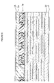
- FIG. 1 illustrates a sectional view of a partially finished multi-layered PCB with an outer copper layer being covered with a polymer layer.
- FIG. 2 illustrates a sectional view of a partially finished multi-layered PCB with a second polymer layer on top of the first polymer layer.
- FIG. 3 illustrates a sectional view of the first and second polymer layers channeled by laser ablation.
- FIG. 3 a illustrates a sectional view of the surface copper layer marked with a unique, easily recognizable pattern.
- FIG. 4 illustrates a sectional view of the multi-layered PCB after an additional coat of the first polymer material has been layered, over the top polymer layer, filling in the laser created channels.
- FIG. 5 illustrates a sectional view of the multi-layered PCB further channeled in the location where through-hole will be drilled.
- FIG. 6 illustrates a sectional view of the multi-layered PCB after “prepeg” and copper foil has been pressed in place prior to the insertion of through-holes.
- FIG. 7 illustrates a sectional view of the multi-layered PCB after drilling of a through-hole.
- FIG. 1 a sectional view is illustrated of a multi-layered PCB with the outer most layers of copper, at an initial stage of optical integration.
- a multi-layered PCB 14 is covered top and bottom with copper layers 10 , 11 .
- the PCB is first built for supporting electrical circuitry and functions, and then incorporates an optical conductive layer into its structure.
- the core of the multi-layer PCB is processed before laminating a first optical conductive layer 12 .
- the optical conductive layer 12 is a polymer material sold under the tradename PolyguideTM.
- the first polymer laminate layer 12 has a specific refraction index n 2 .
- the laminate covers the entire top surface area of the PCB, over the top copper layer 10 .
- the top copper layer 10 is roughened prior to laminating the surface with the polymer coat 12 in order to improve adhesion.
- a chemical, mechanical or combination chemical and mechanical abrasion process may be used.
- Other abrasion processes as known may be employed.
- the optical polymer material is best suited for practice of the present invention if it has the following characteristics: good optical properties (i.e. low dispersion); high temperature and abrasion resistance to avoid damage to the material during fabrication and assembly; and a Z-axis coefficient of expansion comparable to the glass reinforced material used in the PCB.
- a typical epoxy based system has a thermal expansion coefficient (CTE) in the range of 100–150 ppm in the Z-axis.
- CTE in the X-axis and Y-axis is in the range of 16–18 ppm.
- FIG. 2 a sectional view of a partially finished multi-layered PCB is illustrated at a subsequent stage of processing, with a second polymer layer on top of the first polymer layer.
- a second polymer layer 16 is laminated on top of the first polymer layer 12 .
- the second polymer layer 16 covers the entire top surface area.
- the second polymer layer 16 requires the same properties as the first polymer layer 12 .
- the second polymer laminate has a specific refraction index n 1 .
- Refraction index n 1 is greater than refraction index n 2 .
- the optical signal is transmitted in the n 1 index layer.
- FIG. 3 a sectional view is illustrated of the first and second polymer layers channeled by laser ablation.
- the two optical conductive polymer layers 12 , 16 are channeled creating a void 18 in the first and second polymer layers.
- laser ablation is used.
- the laser has an automatic depth control.
- the laser has insufficient energy to cut the copper layer 10 .
- the copper integrity is maintained so that the dielectric layer 20 just below the copper layer is not penetrated.
- Other methods and processes that create cavities or voids in the two polymer layers down to the copper layer 10 will not affect the implementation of the present invention.
- FIG. 3 a a sectional view is illustrated of the surface copper layer marked with a unique, easily recognizable pattern.
- the copper is marked in some of the locations where the polymer layers have been voided 18 .
- One implementation of the present invention etches or marks the copper layer to create a target 22 for alignment of laser ablation processes.
- the targets 22 are positioned so as not to interfere with the circuitry and PCB design logic.
- An embodiment of the present invention places these “alignment” targets or features on the edges of PCB. Multiple marks are used; the more marks the greater the accuracy.
- the targets 22 are uniquely shaped so as to facilitate automatic recognition.
- the copper is etched with chemicals.
- the present invention uses a laser to mark the alignment feature in the copper layer.
- the present invention uses a mechanical process to mark the copper targets.
- FIG. 4 a sectional view is illustrated of a multi-layered PCB after an additional coat of the first polymer material has been layered over the top polymer layer, filling in the laser created channels.
- a third polymer layer 24 is laminated over the top surface of the PCB, covering the PCB to a uniform thickness.
- the voids created by laser ablation are filled.
- the third polymer layer is of the same refraction index, n 2 , as the first polymer layer 12 .
- n 2 refraction index
- the optical waveguides are surrounded by polymer material with lesser refraction index n 2 .
- optical waveguide islands 16 transmit optical signals and allow inter-circuit board connectivity via an optical backplane without the need for electrical cabling.
- the laser ablation process defines the optical waveguides, writing the connection scheme for the PCB and backplane.
- Other passive components such as multiplexers, de-multiplexers, transducers and interferometers are also integrated in the circuitry to effect optical signaling.
- the optical waveguides transmit the optical signals allowing inter-board communications.
- FIG. 5 a sectional view is illustrated of the multi-layered PCB further channeled in the location where a through-hole will be drilled. Where a through-hole is to be located, a void 25 is created in the multiple layers of polymer above the top copper layer 10 . As described supra, laser ablation process is employed to remove the polymer material 12 , 16 , 24 to the copper layer 10 . It is noted that other processes, not herein described, that remove (i.e. channel) polymer layers in the multi-layered PCB will allow the present invention to be practiced.
- prepeg 26 (a non-conductive material) is pressed (laminated) on the top and bottom surfaces of the PCB.
- a layer of copper foil 28 is then pressed on each side to finish the layered PCB in anticipation of inserting through-holes.
- FIG. 7 a sectional view of the multi-layered PCB after drilling of a through-hole is illustrated.
- a through-hole 30 is then inserted.
- One embodiment of the present invention inserts the through-hole by a mechanical drilling of the multi-layered PCB.
- the through-hole 30 is used for mounting components or used as a via hole to access internal layers of the PCB.
- the removal of polymer material does not compromise the through-hole integrity.
- the prepeg material 26 maintains the sidewalls of the through-hole. Note that the optical waveguides 16 are preserved.
Abstract
Description
Claims (19)
Priority Applications (2)
| Application Number | Priority Date | Filing Date | Title |
|---|---|---|---|
| US11/016,146 US7024086B2 (en) | 2001-07-06 | 2004-12-17 | System and method for integrating optical layers in a PCB for inter-board communications |
| US11/375,320 US20060165345A1 (en) | 2001-07-06 | 2006-03-14 | System and method for integrating optical layers in a PCB for inter-board communications |
Applications Claiming Priority (3)
| Application Number | Priority Date | Filing Date | Title |
|---|---|---|---|
| US30338001P | 2001-07-06 | 2001-07-06 | |
| US10/179,758 US6834131B2 (en) | 2001-07-06 | 2002-06-25 | System and method for integrating optical layers in a PCB for inter-board communications |
| US11/016,146 US7024086B2 (en) | 2001-07-06 | 2004-12-17 | System and method for integrating optical layers in a PCB for inter-board communications |
Related Parent Applications (1)
| Application Number | Title | Priority Date | Filing Date |
|---|---|---|---|
| US10/179,758 Continuation US6834131B2 (en) | 2001-07-06 | 2002-06-25 | System and method for integrating optical layers in a PCB for inter-board communications |
Related Child Applications (1)
| Application Number | Title | Priority Date | Filing Date |
|---|---|---|---|
| US11/375,320 Continuation US20060165345A1 (en) | 2001-07-06 | 2006-03-14 | System and method for integrating optical layers in a PCB for inter-board communications |
Publications (2)
| Publication Number | Publication Date |
|---|---|
| US20050129349A1 US20050129349A1 (en) | 2005-06-16 |
| US7024086B2 true US7024086B2 (en) | 2006-04-04 |
Family
ID=23171822
Family Applications (3)
| Application Number | Title | Priority Date | Filing Date |
|---|---|---|---|
| US10/179,758 Expired - Lifetime US6834131B2 (en) | 2001-07-06 | 2002-06-25 | System and method for integrating optical layers in a PCB for inter-board communications |
| US11/016,146 Expired - Fee Related US7024086B2 (en) | 2001-07-06 | 2004-12-17 | System and method for integrating optical layers in a PCB for inter-board communications |
| US11/375,320 Abandoned US20060165345A1 (en) | 2001-07-06 | 2006-03-14 | System and method for integrating optical layers in a PCB for inter-board communications |
Family Applications Before (1)
| Application Number | Title | Priority Date | Filing Date |
|---|---|---|---|
| US10/179,758 Expired - Lifetime US6834131B2 (en) | 2001-07-06 | 2002-06-25 | System and method for integrating optical layers in a PCB for inter-board communications |
Family Applications After (1)
| Application Number | Title | Priority Date | Filing Date |
|---|---|---|---|
| US11/375,320 Abandoned US20060165345A1 (en) | 2001-07-06 | 2006-03-14 | System and method for integrating optical layers in a PCB for inter-board communications |
Country Status (7)
| Country | Link |
|---|---|
| US (3) | US6834131B2 (en) |
| EP (1) | EP1405446A4 (en) |
| JP (1) | JP3666752B2 (en) |
| KR (1) | KR20040035673A (en) |
| CN (2) | CN1870862A (en) |
| HK (1) | HK1068838A1 (en) |
| WO (1) | WO2003005616A2 (en) |
Cited By (5)
| Publication number | Priority date | Publication date | Assignee | Title |
|---|---|---|---|---|
| US20060165345A1 (en) * | 2001-07-06 | 2006-07-27 | Tourne Joseph A | System and method for integrating optical layers in a PCB for inter-board communications |
| US20070086696A1 (en) * | 2005-10-17 | 2007-04-19 | Shih-Ping Hsu | Circuit board structure of integrated optoelectronic component |
| US20070154132A1 (en) * | 2005-12-29 | 2007-07-05 | Intel Corporation | Optical and/or electrical communications fabrics in circuit boards and/or other composite structures |
| US20080304832A1 (en) * | 2007-06-11 | 2008-12-11 | Williams R Stanley | Optical interconnect |
| US10141623B2 (en) | 2016-10-17 | 2018-11-27 | International Business Machines Corporation | Multi-layer printed circuit board having first and second coaxial vias coupled to a core of a dielectric waveguide disposed in the circuit board |
Families Citing this family (19)
| Publication number | Priority date | Publication date | Assignee | Title |
|---|---|---|---|---|
| US7405364B2 (en) * | 2002-12-30 | 2008-07-29 | Intel Corporation | Decoupled signal-power substrate architecture |
| DE10347331A1 (en) * | 2003-10-10 | 2005-05-04 | Univ Dortmund | Process for the production of electro-optical circuit boards with polysiloxane waveguides and their use |
| KR20050040589A (en) * | 2003-10-29 | 2005-05-03 | 삼성전기주식회사 | Painted circuit board having the waveguide and manufacturing method thereof |
| TWI294258B (en) * | 2004-08-03 | 2008-03-01 | Rohm & Haas Elect Mat | Methods of forming devices having optical functionality |
| TW200623993A (en) | 2004-08-19 | 2006-07-01 | Rohm & Haas Elect Mat | Methods of forming printed circuit boards |
| EP1674905B1 (en) | 2004-12-22 | 2008-10-15 | Rohm and Haas Electronic Materials, L.L.C. | Methods of forming optical devices having polymeric layers |
| DE602005011393D1 (en) | 2004-12-22 | 2009-01-15 | Rohm & Haas Elect Mat | Dry optical films and methods of making dry film optical devices |
| DE602005011394D1 (en) | 2004-12-22 | 2009-01-15 | Rohm & Haas Elect Mat | Dry optical films and methods of making dry film optical devices |
| DE102005053202A1 (en) * | 2005-11-08 | 2007-05-10 | Comet Gmbh | Apparatus for preparing a multilayer printed circuit board for drilling via holes |
| US20080044130A1 (en) * | 2006-08-16 | 2008-02-21 | Xyratex Technology Limited | Optical printed circuit board, a method of making an optical printed circuit board and an optical waveguide |
| KR101084407B1 (en) * | 2006-12-26 | 2011-11-18 | 미쓰이 가가쿠 가부시키가이샤 | Optical/electrical mixture mounting board and method for producing the same |
| JP2008166798A (en) | 2006-12-31 | 2008-07-17 | Rohm & Haas Electronic Materials Llc | Method for forming printed circuit board having optical functions |
| KR101531054B1 (en) * | 2008-09-12 | 2015-06-23 | 주식회사 엔씨소프트 | Apprartus and method of transmitting geometric information in integrated messing circumstance |
| AT12322U1 (en) * | 2009-01-27 | 2012-03-15 | Dcc Dev Circuits & Components Gmbh | METHOD FOR THE PRODUCTION OF A MULTILAYER CONDUCTOR PLATE, ANTI-TEMPERATURE MATERIAL AND MULTILAYER CONDUCTOR PLATE AND USE OF SUCH A PROCESS |
| US7949211B1 (en) | 2010-02-26 | 2011-05-24 | Corning Incorporated | Modular active board subassemblies and printed wiring boards comprising the same |
| US8731343B2 (en) | 2011-02-24 | 2014-05-20 | Xyratex Technology Limited | Optical printed circuit board, a method of making an optical printed circuit board and an optical waveguide |
| US9081137B2 (en) | 2013-01-21 | 2015-07-14 | International Business Machines Corporation | Implementing embedded hybrid electrical-optical PCB construct |
| CN111901963B (en) * | 2019-05-05 | 2022-01-04 | 诺沛半导体有限公司 | Method for forming welding pad on LED carrier plate |
| WO2021092463A1 (en) * | 2019-11-06 | 2021-05-14 | Ttm Technologies Inc. | Systems and methods for removing undesired metal within vias from printed circuit boards |
Citations (12)
| Publication number | Priority date | Publication date | Assignee | Title |
|---|---|---|---|---|
| US3972755A (en) | 1972-12-14 | 1976-08-03 | The United States Of America As Represented By The Secretary Of The Navy | Dielectric circuit board bonding |
| US5054870A (en) | 1989-04-03 | 1991-10-08 | Alcatel N.V. | Electro-optical multiple connection arrangement |
| US5263111A (en) | 1991-04-15 | 1993-11-16 | Raychem Corporation | Optical waveguide structures and formation methods |
| US5680698A (en) | 1994-12-07 | 1997-10-28 | Lucent Technologies Inc. | Method for precise alignment and placement of optoelectric components |
| US5808272A (en) | 1994-11-22 | 1998-09-15 | Electro Scientific Industries, Inc. | Laser system for functional trimming of films and devices |
| US5891795A (en) | 1996-03-18 | 1999-04-06 | Motorola, Inc. | High density interconnect substrate |
| US6185354B1 (en) | 1998-05-15 | 2001-02-06 | Motorola, Inc. | Printed circuit board having integral waveguide |
| US6370292B1 (en) | 1998-08-25 | 2002-04-09 | Robert Bosch Gmbh | Printed circuit board and method for its manufacture |
| US6611635B1 (en) | 1998-10-09 | 2003-08-26 | Fujitsu Limited | Opto-electronic substrates with electrical and optical interconnections and methods for making |
| US6705124B2 (en) * | 2001-06-04 | 2004-03-16 | Lightwave Microsystems Corporation | High-density plasma deposition process for fabricating a top clad for planar lightwave circuit devices |
| US6760497B1 (en) | 1999-02-23 | 2004-07-06 | Ppc Electronic Ag | Printed circuit board for electrical and optical signals and method for producing the same |
| US6834131B2 (en) * | 2001-07-06 | 2004-12-21 | Viasystems Group, Inc. | System and method for integrating optical layers in a PCB for inter-board communications |
Family Cites Families (6)
| Publication number | Priority date | Publication date | Assignee | Title |
|---|---|---|---|---|
| US5106211A (en) * | 1991-02-14 | 1992-04-21 | Hoechst Celanese Corp. | Formation of polymer channel waveguides by excimer laser ablation and method of making same |
| US6274391B1 (en) * | 1992-10-26 | 2001-08-14 | Texas Instruments Incorporated | HDI land grid array packaged device having electrical and optical interconnects |
| DE69842092D1 (en) * | 1997-12-11 | 2011-02-17 | Ibiden Co Ltd | Method for producing a multilayer printed circuit board |
| US6684007B2 (en) * | 1998-10-09 | 2004-01-27 | Fujitsu Limited | Optical coupling structures and the fabrication processes |
| TW460717B (en) * | 1999-03-30 | 2001-10-21 | Toppan Printing Co Ltd | Optical wiring layer, optoelectric wiring substrate mounted substrate, and methods for manufacturing the same |
| US6731857B2 (en) * | 2001-03-29 | 2004-05-04 | Shipley Company, L.L.C. | Photodefinable composition, method of manufacturing an optical waveguide with the photodefinable composition, and optical waveguide formed therefrom |
-
2002
- 2002-06-24 WO PCT/US2002/019840 patent/WO2003005616A2/en active Application Filing
- 2002-06-24 JP JP2003511455A patent/JP3666752B2/en not_active Expired - Fee Related
- 2002-06-24 CN CNA2006100785695A patent/CN1870862A/en active Pending
- 2002-06-24 CN CNB028136446A patent/CN1281367C/en not_active Expired - Fee Related
- 2002-06-24 KR KR10-2004-7000162A patent/KR20040035673A/en not_active Application Discontinuation
- 2002-06-24 EP EP02739953A patent/EP1405446A4/en not_active Withdrawn
- 2002-06-25 US US10/179,758 patent/US6834131B2/en not_active Expired - Lifetime
-
2004
- 2004-12-17 US US11/016,146 patent/US7024086B2/en not_active Expired - Fee Related
- 2004-12-29 HK HK04110314A patent/HK1068838A1/en not_active IP Right Cessation
-
2006
- 2006-03-14 US US11/375,320 patent/US20060165345A1/en not_active Abandoned
Patent Citations (12)
| Publication number | Priority date | Publication date | Assignee | Title |
|---|---|---|---|---|
| US3972755A (en) | 1972-12-14 | 1976-08-03 | The United States Of America As Represented By The Secretary Of The Navy | Dielectric circuit board bonding |
| US5054870A (en) | 1989-04-03 | 1991-10-08 | Alcatel N.V. | Electro-optical multiple connection arrangement |
| US5263111A (en) | 1991-04-15 | 1993-11-16 | Raychem Corporation | Optical waveguide structures and formation methods |
| US5808272A (en) | 1994-11-22 | 1998-09-15 | Electro Scientific Industries, Inc. | Laser system for functional trimming of films and devices |
| US5680698A (en) | 1994-12-07 | 1997-10-28 | Lucent Technologies Inc. | Method for precise alignment and placement of optoelectric components |
| US5891795A (en) | 1996-03-18 | 1999-04-06 | Motorola, Inc. | High density interconnect substrate |
| US6185354B1 (en) | 1998-05-15 | 2001-02-06 | Motorola, Inc. | Printed circuit board having integral waveguide |
| US6370292B1 (en) | 1998-08-25 | 2002-04-09 | Robert Bosch Gmbh | Printed circuit board and method for its manufacture |
| US6611635B1 (en) | 1998-10-09 | 2003-08-26 | Fujitsu Limited | Opto-electronic substrates with electrical and optical interconnections and methods for making |
| US6760497B1 (en) | 1999-02-23 | 2004-07-06 | Ppc Electronic Ag | Printed circuit board for electrical and optical signals and method for producing the same |
| US6705124B2 (en) * | 2001-06-04 | 2004-03-16 | Lightwave Microsystems Corporation | High-density plasma deposition process for fabricating a top clad for planar lightwave circuit devices |
| US6834131B2 (en) * | 2001-07-06 | 2004-12-21 | Viasystems Group, Inc. | System and method for integrating optical layers in a PCB for inter-board communications |
Cited By (8)
| Publication number | Priority date | Publication date | Assignee | Title |
|---|---|---|---|---|
| US20060165345A1 (en) * | 2001-07-06 | 2006-07-27 | Tourne Joseph A | System and method for integrating optical layers in a PCB for inter-board communications |
| US20070086696A1 (en) * | 2005-10-17 | 2007-04-19 | Shih-Ping Hsu | Circuit board structure of integrated optoelectronic component |
| US7302126B2 (en) * | 2005-10-17 | 2007-11-27 | Phoenix Precision Technology Corporation | Circuit board structure of integrated optoelectronic componenet |
| US20070154132A1 (en) * | 2005-12-29 | 2007-07-05 | Intel Corporation | Optical and/or electrical communications fabrics in circuit boards and/or other composite structures |
| US7496249B2 (en) * | 2005-12-29 | 2009-02-24 | Intel Corporation | Optical and/or electrical communications fabrics in circuit boards and/or other composite structures |
| US20080304832A1 (en) * | 2007-06-11 | 2008-12-11 | Williams R Stanley | Optical interconnect |
| US8009992B2 (en) | 2007-06-11 | 2011-08-30 | Hewlett-Packard Development Company, L.P. | Optical interconnect |
| US10141623B2 (en) | 2016-10-17 | 2018-11-27 | International Business Machines Corporation | Multi-layer printed circuit board having first and second coaxial vias coupled to a core of a dielectric waveguide disposed in the circuit board |
Also Published As
| Publication number | Publication date |
|---|---|
| CN1281367C (en) | 2006-10-25 |
| JP3666752B2 (en) | 2005-06-29 |
| US6834131B2 (en) | 2004-12-21 |
| US20030006068A1 (en) | 2003-01-09 |
| US20060165345A1 (en) | 2006-07-27 |
| WO2003005616A3 (en) | 2003-03-20 |
| CN1870862A (en) | 2006-11-29 |
| EP1405446A2 (en) | 2004-04-07 |
| CN1524026A (en) | 2004-08-25 |
| WO2003005616A2 (en) | 2003-01-16 |
| HK1068838A1 (en) | 2005-05-06 |
| JP2004535070A (en) | 2004-11-18 |
| EP1405446A4 (en) | 2006-07-19 |
| KR20040035673A (en) | 2004-04-29 |
| US20050129349A1 (en) | 2005-06-16 |
Similar Documents
| Publication | Publication Date | Title |
|---|---|---|
| US20060165345A1 (en) | System and method for integrating optical layers in a PCB for inter-board communications | |
| US9417415B2 (en) | Interposer with polymer-filled or polymer-lined optical through-vias in thin glass substrate | |
| KR100952478B1 (en) | Printed Circuit Board and Manufacturing Method Thereof | |
| US5925206A (en) | Practical method to make blind vias in circuit boards and other substrates | |
| US8340480B2 (en) | Opto-electrical hybrid wiring board and method for manufacturing the same | |
| Lehmacher et al. | Integration of polymer optical waveguides into printed circuit boards | |
| CA2347568C (en) | Circuit board and method of manufacturing a circuit board | |
| EP2800463A1 (en) | Printed circuit board and fabricating method thereof | |
| US6996305B2 (en) | Printed circuit board with opto-via holes and process of forming the opto-via holes | |
| WO2008004382A1 (en) | Method for manufacturing multilayer printed wiring board | |
| KR20060118647A (en) | A method for manufacturing optical-waveguides, optical-electricity pcb with the optical-waveguides and method for manufacturing the same | |
| US7697800B2 (en) | Method of manufacturing printed circuit board | |
| CN112867286A (en) | Preparation method of embedded large copper plate back plate | |
| KR20040049218A (en) | A multi-layer PCB for connecting multi-channel optical signals of block type, and methods thereof | |
| US20070269159A1 (en) | Flexible Printed Circuits Capable of Transmitting Electrical and Optical Signals | |
| US8979372B2 (en) | Circuit board and manufacturing method thereof and electro-optic apparatus having the circuit board | |
| AU2002312569A1 (en) | System and method for integrating optical layers in a PCB for inter-board communications | |
| CN101778534A (en) | Photoelectric mixed circuit board and manufacturing method thereof | |
| JP2004146668A (en) | Multilayer printed circuit board and manufacturing method thereof | |
| JP2005150671A (en) | Printed circuit board and its manufacturing method | |
| CN113225917A (en) | Method for manufacturing circuit board with back drilling hole | |
| KR20050041728A (en) | Fabricating method of printed circuit board equipping optical fiber |
Legal Events
| Date | Code | Title | Description |
|---|---|---|---|
| AS | Assignment |
Owner name: VIASYSTEMS GROUP, INC., MISSOURI Free format text: ASSIGNMENT OF ASSIGNORS INTEREST;ASSIGNOR:TOURNE, JOSEPH A.A.M.;REEL/FRAME:021040/0597 Effective date: 20020905 |
|
| FEPP | Fee payment procedure |
Free format text: PAYOR NUMBER ASSIGNED (ORIGINAL EVENT CODE: ASPN); ENTITY STATUS OF PATENT OWNER: LARGE ENTITY |
|
| FPAY | Fee payment |
Year of fee payment: 4 |
|
| AS | Assignment |
Owner name: VIASYSTEMS, INC.,MISSOURI Free format text: ASSIGNMENT OF ASSIGNORS INTEREST;ASSIGNOR:VIASYSTEMS GROUP, INC.;REEL/FRAME:023905/0147 Effective date: 20100205 |
|
| AS | Assignment |
Owner name: WACHOVIA CAPITAL FINANCE CORPORATION (NEW ENGLAND) Free format text: SECURITY AGREEMENT;ASSIGNOR:VIASYSTEMS, INC.;REEL/FRAME:024062/0634 Effective date: 20100216 |
|
| AS | Assignment |
Owner name: WILMINGTON TRUST, NATIONAL ASSOCIATION, AS COLLATE Free format text: SECURITY AGREEMENT;ASSIGNORS:VIASYSTEMS, INC.;VIASYSTEMS CORPORATION;REEL/FRAME:028158/0575 Effective date: 20120430 |
|
| FPAY | Fee payment |
Year of fee payment: 8 |
|
| AS | Assignment |
Owner name: VIASYSTEMS, INC., MISSOURI Free format text: RELEASE BY SECURED PARTY;ASSIGNOR:WACHOVIA CAPITAL FINANCE CORPORATION (NEW ENGLAND);REEL/FRAME:035850/0669 Effective date: 20150601 Owner name: JPMORGAN CHASE BANK, N.A., AS ADMINISTRATIVE AGENT Free format text: PATENT SECURITY AGREEMENT-TERM;ASSIGNORS:TTM TECHNOLOGIES, INC.;VIASYSTEMS, INC.;VIASYSTEMS TECHNOLOGIES CORP., L.L.C.;REEL/FRAME:035851/0928 Effective date: 20150531 Owner name: VIASYSTEMS, INC., MISSOURI Free format text: RELEASE BY SECURED PARTY;ASSIGNOR:WILMINGTON TRUST, NATIONAL ASSOCIATION;REEL/FRAME:035858/0092 Effective date: 20150601 Owner name: VIASYSTEMS CORPORATION (FORMERLY MERIX CORPORATION Free format text: RELEASE BY SECURED PARTY;ASSIGNOR:WILMINGTON TRUST, NATIONAL ASSOCIATION;REEL/FRAME:035858/0092 Effective date: 20150601 Owner name: JPMORGAN CHASE BANK, N.A., AS ADMINISTRATIVE AGENT Free format text: PATENT SECURITY AGREEMENT-ABL;ASSIGNORS:TTM TECHNOLOGIES, INC.;VIASYSTEMS, INC.;VIASYSTEMS TECHNOLOGIES CORP., L.L.C.;REEL/FRAME:035858/0890 Effective date: 20150531 |
|
| FEPP | Fee payment procedure |
Free format text: MAINTENANCE FEE REMINDER MAILED (ORIGINAL EVENT CODE: REM.) |
|
| LAPS | Lapse for failure to pay maintenance fees |
Free format text: PATENT EXPIRED FOR FAILURE TO PAY MAINTENANCE FEES (ORIGINAL EVENT CODE: EXP.) |
|
| STCH | Information on status: patent discontinuation |
Free format text: PATENT EXPIRED DUE TO NONPAYMENT OF MAINTENANCE FEES UNDER 37 CFR 1.362 |
|
| FP | Lapsed due to failure to pay maintenance fee |
Effective date: 20180404 |
|
| AS | Assignment |
Owner name: VIASYSTEMS GROUP, INC., CALIFORNIA Free format text: MERGER;ASSIGNOR:VIASYSTEMS, INC.;REEL/FRAME:063628/0122 Effective date: 20171027 Owner name: TTM TECHNOLOGIES, INC., CALIFORNIA Free format text: MERGER;ASSIGNOR:VIASYSTEMS GROUP, INC.;REEL/FRAME:063629/0313 Effective date: 20171030 |