US7023227B1 - Apparatus for socketing and testing integrated circuits and methods of operating the same - Google Patents
Apparatus for socketing and testing integrated circuits and methods of operating the same Download PDFInfo
- Publication number
- US7023227B1 US7023227B1 US10/075,832 US7583202A US7023227B1 US 7023227 B1 US7023227 B1 US 7023227B1 US 7583202 A US7583202 A US 7583202A US 7023227 B1 US7023227 B1 US 7023227B1
- Authority
- US
- United States
- Prior art keywords
- under test
- device under
- circuit board
- printed circuit
- set forth
- Prior art date
- Legal status (The legal status is an assumption and is not a legal conclusion. Google has not performed a legal analysis and makes no representation as to the accuracy of the status listed.)
- Expired - Lifetime, expires
Links
Images


Classifications
-
- G—PHYSICS
- G01—MEASURING; TESTING
- G01R—MEASURING ELECTRIC VARIABLES; MEASURING MAGNETIC VARIABLES
- G01R31/00—Arrangements for testing electric properties; Arrangements for locating electric faults; Arrangements for electrical testing characterised by what is being tested not provided for elsewhere
- G01R31/28—Testing of electronic circuits, e.g. by signal tracer
- G01R31/2851—Testing of integrated circuits [IC]
- G01R31/2893—Handling, conveying or loading, e.g. belts, boats, vacuum fingers
Landscapes
- Engineering & Computer Science (AREA)
- Computer Hardware Design (AREA)
- Microelectronics & Electronic Packaging (AREA)
- General Engineering & Computer Science (AREA)
- Physics & Mathematics (AREA)
- General Physics & Mathematics (AREA)
- Testing Of Individual Semiconductor Devices (AREA)
Abstract
There is disclosed apparatus for socketing and testing integrated circuits, particularly RF and high-frequency integrated circuits in high density and fine pitch packages, and methods of operating the same. An exemplary apparatus includes an air machine and a housing. The housing includes a universal printed circuit board that is operable to receive a device under test, a controller that is operable to control testing of the received device under test, and a power supply. The housing and the air machine are associable to form an at least substantially air-tight chamber ensconcing the received device under test.
Description
The present invention is directed to apparatus for socketing and testing integrated circuits, particularly RF and high-frequency integrated circuits, and methods of operating the same.
An integrated circuit (“IC”) may be defined broadly as any small electronic device comprising semiconductor material. ICs are designed to meet certain design specifications and are often classified by the number of transistors and other electronic components they contain.
ICs are tested during their respective design, development and manufacture stages to identify and eliminate potential defects. Such testing is commonly performed in a non-destructive manner to determine whether the ICs under test meet their respective specifications. For instance, assuming a relatively simple device (e.g., a device with only a few input and output terminals or “pins”), testing may involve applying signals to the input terminals, measuring the response on the output terminals, and comparing the actual response to the designed response. As errors are observed between the designed and actual output signal states, design problems in the ICs or in the load board may be pinpointed and remedied.
Over the years, the semiconductor industry has had a constant challenge maintaining its pace with the advances in IC-packaging technology. This challenge is exacerbated when evaluating radio-frequency (“RF”) ICs due to their heightened sensitivity to parasitic elements and requirement of “good” matching (e.g., input/output (“I/O”) impedance, interconnect, support components, etc.).
One common socket and test approach, for instance, utilizes a conventional clamping mechanism to securing “tssop”-IC packages to printed circuit boards (“PCBs”). This approach is cumbersome and fails to provide a mechanism to aid registration of device pins to pads on the PCB, thereby requiring an operator to align device pins with the pads by trial and error. Further, the jigs used for socketing the device under test (“DUT”) commonly require manual mechanical adjustments.
Another more contemporary approach utilizes a “drill-press” like jig to accommodate ball-grid array and quad-flat-pack packaged devices. This approach is also cumbersome and the jig often prohibits die probing and significantly interferes with environmental stress testing. In contrast to the prior approach which utilized a large lever mechanism (commonly from below the DUT board) to effect the press action, this more contemporary approach utilizes a soft adjustable tension plunger (commonly from above the DUT board).
A further complication is that PCBs used in the test platforms are not standardized (e.g., general dimensions, plating parameter, I/O port spacing, etc.), as each engineer typically designs their “PCB” to fit a particular DUT. There is therefore a need in the art for an apparatus for socketing and testing a DUT having suitable tolerance control over electro-mechanical contact between pad and pin. There is a further need in the art for a universal core PCB employed with standard I/O connectors for use with DUTs. There is a yet further need in the art for standardized sockets developed for dual-in-line “tssop” and quad-flat-pack packages to replace the bulky clamping mechanisms widely used in the semiconductor industry.
To address the above-discussed deficiencies of the prior art, it is a primary object of the present invention to provide apparatus for socketing and testing ICs, particularly RF and high-frequency ICs in high density and fine pitch packages (i.e., chip scale, tssop, tqfp, etc.), and methods of operating the same.
According to an advantageous embodiment hereof, an apparatus is introduced for socketing and testing ICs, and includes an air machine and a housing. The housing includes a universal PCB that is operable to receive a DUT, a controller that is operable to control testing of the received DUT, and a power supply. The housing and the air machine are associable to form an at least substantially air-tight chamber ensconcing the received DUT.
According to an advantageous embodiment, the PCB is circular in shape, and the housing further includes I/O connectors that are placed circumferentially and symmetrically near the edge of the universal printed circuit board. In a related embodiment, the PCB includes a leadless, self-registering socket that is operable to receive the DUT and its support components (if any) in the center of the PCB. The PCB may advantageously include gold fuse dotted arrays embedded in soft membrane which can be used as contactors in sockets for ball grid array packages.
It is important to note that the self-registering and leadless socket adds no additional inductance between the DUT and the PCB during operation. Further, use of a clamp-shell top with a large center opening enables both a thermally/cryogenically treated air stream to blanket the DUT, and micro-probing of the DUT. In addition, it is desirable to have an at least substantially air-tight seal between the air machine and the housing to prevent moisture buildup, icing or the like.
The foregoing has outlined rather broadly the features and technical advantages of the present invention so that those skilled in the art may better understand the detailed description of the invention that follows. Additional features and advantages of the invention will be described hereinafter that form the subject of the claims of the invention. Those skilled in the art should appreciate that they may readily use the conception and the specific embodiment disclosed as a basis for modifying or designing other structures for carrying out the same purposes of the present invention. Those skilled in the art should also realize that such equivalent constructions do not depart from the spirit and scope of the invention in its broadest form.
Before undertaking the DETAILED DESCRIPTION OF THE INVENTION below, it may be advantageous to set forth definitions of certain words and phrases used throughout this patent document: the terms “include” and “comprise,” as well as derivatives thereof, mean inclusion without limitation; the term “or,” is inclusive, meaning and/or; the phrases “associated with” and “associated therewith,” as well as derivatives thereof, may mean to include, be included within, interconnect with, contain, be contained within, connect to or with, couple to or with, be communicable with, cooperate with, interleave, juxtapose, be proximate to, be bound to or with, have, have a property of, or the like; and the term “controller” means any device, system or part thereof that controls at least one operation, such a device may be implemented in hardware, firmware or software, or some combination of at least two of the same. It should be noted that the functionality associated with any particular controller may be centralized or distributed, whether locally or remotely. Definitions for certain words and phrases are provided throughout this patent document, those of ordinary skill in the art should understand that in many, if not most instances, such definitions apply to prior, as well as future uses of such defined words and phrases.
For a more complete understanding of the present invention, and the advantages thereof, reference is now made to the following descriptions taken in conjunction with the accompanying drawings, wherein like numbers designate like objects, and in which:
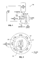
Exemplary housing 110 illustratively includes a first housing-layer 120, a second housing-layer 125, a PCB 130, a DUT 135, I/O connectors 140, a controller 145 and a power supply 150. Exemplary first and second housing-layers 120; 125, as well as the remainder of housing 110 are made from one or more physiologically acceptable materials suitable for IC-testing apparatus.
According to the illustrated implementation, first housing-layer 120 is associated with second housing-layer 125 and includes an aperture (shown in FIGS. 2 and 3 ) that is sized and shaped to mate with interface 115. According to the present embodiment, interface 115 includes a suitably arranged insulating gasket that operates to at least substantially seal the association of interface 115 with the aperture of first housing-layer 120. It is desirable to have an at least substantially air-tight seal between interface 115 and first housing-layer 120 to prevent moisture buildup, icing or the like.
Exemplary PCB 130 is a universal circular core PCB employed with standard SMA I/O connectors 140 placed circumferentially and symmetrically near the edge of PCB 130. According to the present embodiment, PCB 130 advantageously includes (i) a plurality of “leadless” sockets developed for dual in-line “tssop” and quad-flat-pack packages that are used in place of the above-described clamping mechanisms widely used in the PRIOR ART, and (ii) gold-fuse-dotted arrays that are used as contactors in sockets for ball-grid array packages.
Exemplary I/O connectors 140 illustratively provide standardized SMA I/O ports configured radially at the perimeter of circular PCB 130 to facilitate signal line trace matching and minimize parasitic element coupling.
Finally, it should be noted that the illustrated implementation may be suitable for use in an electrostatic and magnetic (“E&M”) shielded chamber, as apparatus 100 provides a sufficiently self-contained test jig suitable for use inside a Faraday Cage for accurate measurements.
According to an advantageous embodiment hereof, the metallurgical composition of the conductors and dielectric material of PCB 130 to achieve optimal contact and flatness for the top surface metal finish are as follows: (i) from insulator (e.g., fiber glass or polyamide) start with approximately a 0.1 mil copper thickness; (ii) plate the copper up to 4.0 mil thick minimum; (iii) nickel plate (bright nickel) 250 micro inches, 350 micro inches preferred on copper; and (iv) plate hard gold 70 micro inches thick minimum, 100 micro inches preferred on nickel.
It is preferred that a pulse-plating (non-DC plating) process is used to attain better electrical characteristics, namely, lower impedance, higher atomic packing density, uniform distribution and flatness of the finished metal layer, which improves high frequency performance. This approach also improves the mechanical strength so that repeated pressure from contacting device pin onto a metal pad tends not to lead to accelerated metal fatigue as in conventional plating processes.
Initially, either manually or via computer automation, I/O device pins are attached to stimuli and data capture/processing instruments via SMA connectors 140 and the desired instruments setting controls are set, and the serial control data bus is connected to a computing/monitoring resource (process step 405; these actions are illustrative in nature only, and will depend on the nature of the DUT).
Next, either manually or via robotic arm, DUT 135 is selected and associated with socket cavity 320 of PCB 130 via “leadless” socket onto PCB 130 (process step 410); integrated power supply 150 is powered “ON” (process step 415); air machine 105 is associated with housing 110 creating an air-tight seal, the desired temperature(s) and cycle times are set and test stimuli are applied to DUT 135 and the desired response data is captured (process step 420); and, finally, integrated power supply 150 is powered “OFF” and DUT 135 is removed (process step 425).
According to the illustrated embodiment, the testing may suitably include applying both signal and pulse stimuli to test apparatus 100 during varying thermal conditions to enable logic, spectrum, phase-noise, phase-error and other like analysis of DUT 135. Apparatus 100 introduces a self-contained test apparatus for ICs, and, in particular RF and high frequency semiconductor devices.
Although the present invention has been described in detail, those skilled in the art should understand that they can make various changes, substitutions and alterations herein without departing from the spirit and scope of the invention in its is broadest form.
Claims (20)
1. An apparatus for socketing and testing integrated circuits comprising:
an air machine that is operable to controllably provide a thermally-varying air flow; and
a housing comprising (i) a printed circuit board that is operable to receive a device under test, the printed circuit board comprising a leadless socket operable to receive the device under test, and (ii) a controller that is operable to control testing of the received device under test;
wherein said air machine is associable with said housing to form an at least substantially air-tight chamber ensconcing the received device under test.
2. The apparatus as set forth in claim 1 wherein said housing further comprises a power supply.
3. The apparatus as set forth in claim 1 wherein said printed circuit board is circular shaped.
4. The apparatus as set forth in claim 3 wherein said housing further comprises input/output (I/O) connectors that are placed circumferentially and symmetrically near the edge of the printed circuit board.
5. The apparatus as set forth in claim 3 wherein the leadless socket is self-registering.
6. The apparatus as set forth in claim 5 wherein said leadless socket is operable to receive the device under test in a center of the printed circuit board.
7. A method of operating an apparatus for socketing and testing integrated circuits, said apparatus comprising an air machine and a housing, said housing comprising a printed circuit board and a controller, said method comprising the steps of:
(i) receiving a device under test at the printed circuit board, the printed circuit board comprising a leadless socket operable to receive the device under test, and
(ii) associating said air machine with said housing to form an at least substantially air-tight chamber ensconcing the received device under test, the air machine operable to controllably provide a thermally-varying air flow.
8. The method as set forth in claim 7 wherein said housing further comprises a power supply, and said method comprising the step of powering on the apparatus.
9. The method as set forth in claim 7 wherein said printed circuit board is circular shaped, and said method comprising the step of controlling testing of the received device under test with said controller.
10. The method as set forth in claim 9 wherein said housing further comprises input/output (I/O) connectors that are placed circumferentially and symmetrically near the edge of the printed circuit board.
11. The method as set forth in claim 9 wherein the leadless socket is self-registering.
12. The method as set forth in claim 11 wherein said leadless socket is operable to receive the device under test in a center of the printed circuit board.
13. The method of claim 7 , further comprising setting one or more desired temperatures and one or more desired cycle times for a test of the integrated circuits.
14. An apparatus for socketing and testing integrated circuits comprising:
an air machine that is operable to controllably provide a thermally-varying air flow; and
a housing comprising (i) a universal printed circuit board that is operable to receive a device under test, the printed circuit board comprising a leadless socket operable to receive the device under test, (ii) a controller that is operable to control testing of the received device under test, and (iii) a power supply;
wherein said air machine is associable with said housing to form an at least substantially air-tight chamber ensconcing the received device under test.
15. The apparatus as set forth in claim 14 wherein said power supply is a battery.
16. The apparatus as set forth in claim 14 wherein said universal printed circuit board is circular shaped.
17. The apparatus as set forth in claim 16 wherein said housing further comprises input/output (I/O) connectors that are placed circumferentially and symmetrically near the edge of the universal printed circuit board.
18. The apparatus as set forth in claim 14 wherein said leadless socket is operable to receive the device under test in a center of the printed circuit board.
19. The apparatus as set forth in claim 14 wherein the device under test is one of a radio frequency (RF) integrated circuit and a high-frequency integrated circuit.
20. The apparatus as set forth in claim 14 wherein said leadless socket is self-registering.
Priority Applications (1)
| Application Number | Priority Date | Filing Date | Title |
|---|---|---|---|
| US10/075,832 US7023227B1 (en) | 2002-02-12 | 2002-02-12 | Apparatus for socketing and testing integrated circuits and methods of operating the same |
Applications Claiming Priority (1)
| Application Number | Priority Date | Filing Date | Title |
|---|---|---|---|
| US10/075,832 US7023227B1 (en) | 2002-02-12 | 2002-02-12 | Apparatus for socketing and testing integrated circuits and methods of operating the same |
Publications (1)
| Publication Number | Publication Date |
|---|---|
| US7023227B1 true US7023227B1 (en) | 2006-04-04 |
Family
ID=36101967
Family Applications (1)
| Application Number | Title | Priority Date | Filing Date |
|---|---|---|---|
| US10/075,832 Expired - Lifetime US7023227B1 (en) | 2002-02-12 | 2002-02-12 | Apparatus for socketing and testing integrated circuits and methods of operating the same |
Country Status (1)
| Country | Link |
|---|---|
| US (1) | US7023227B1 (en) |
Cited By (4)
| Publication number | Priority date | Publication date | Assignee | Title |
|---|---|---|---|---|
| US20060043996A1 (en) * | 2004-08-25 | 2006-03-02 | Hill Gregory S | Construction and use of dielectric plate for mating test equipment to a load board of a circuit tester |
| US20080042679A1 (en) * | 2006-08-16 | 2008-02-21 | Suss Microtec Test Systems Gmbh | Method and apparatus for controlling the temperature of electronic components |
| JP2017518505A (en) * | 2014-06-20 | 2017-07-06 | エクセラ・コーポレーションXcerra Corp. | Test socket assembly and related methods |
| US20190324082A1 (en) * | 2018-04-18 | 2019-10-24 | Advanced Semiconductor Engineering, Inc. | Test apparatus and method for operating the same |
Citations (18)
| Publication number | Priority date | Publication date | Assignee | Title |
|---|---|---|---|---|
| US3710251A (en) * | 1971-04-07 | 1973-01-09 | Collins Radio Co | Microelectric heat exchanger pedestal |
| US4734872A (en) * | 1985-04-30 | 1988-03-29 | Temptronic Corporation | Temperature control for device under test |
| US4782291A (en) * | 1985-10-04 | 1988-11-01 | Blandin Bruce A | Method and apparatus for the testing of active or passive electrical devices in a sub-zero environment |
| US4926117A (en) * | 1988-05-02 | 1990-05-15 | Micron Technology, Inc. | Burn-in board having discrete test capability |
| US4945302A (en) * | 1987-04-24 | 1990-07-31 | Scantest Systems A/S | Process and a circuit board for performing tests during burn-in of integrated semi-conductor circuits |
| US4962355A (en) * | 1988-10-27 | 1990-10-09 | The United States Of America As Represented By The Secretary Of The Army | Thermal test chamber device |
| US5086269A (en) * | 1991-03-08 | 1992-02-04 | Hewlett-Packard Company | Burn-in process and apparatus |
| US5331273A (en) * | 1992-04-10 | 1994-07-19 | The United States Of America As Represented By The Secretary Of The Navy | Thermal fixture for testing an integrated circuit |
| US5451884A (en) * | 1993-08-04 | 1995-09-19 | Transat Corp. | Electronic component temperature test system with flat ring revolving carriage |
| US5929651A (en) * | 1995-08-09 | 1999-07-27 | International Business Machines Corporation | Semiconductor wafer test and burn-in |
| US5952840A (en) * | 1996-12-31 | 1999-09-14 | Micron Technology, Inc. | Apparatus for testing semiconductor wafers |
| US6114868A (en) * | 1996-04-24 | 2000-09-05 | Micron Technology, Inc. | Uniform temperature environmental testing method for semiconductor devices |
| US6157201A (en) * | 1995-04-20 | 2000-12-05 | Sun Microsystems, Inc. | Burn-in system for reliable integrated circuit manufacturing |
| US6169409B1 (en) * | 1997-05-19 | 2001-01-02 | Tokyo Electron Limited | Low-temperature wafer testing method and prober |
| US6288561B1 (en) * | 1988-05-16 | 2001-09-11 | Elm Technology Corporation | Method and apparatus for probing, testing, burn-in, repairing and programming of integrated circuits in a closed environment using a single apparatus |
| US6322626B1 (en) * | 1999-06-08 | 2001-11-27 | Micron Technology, Inc. | Apparatus for controlling a temperature of a microelectronics substrate |
| US6329831B1 (en) * | 1997-08-08 | 2001-12-11 | Advanced Micro Devices, Inc. | Method and apparatus for reliability testing of integrated circuit structures and devices |
| US6501290B2 (en) * | 1999-09-29 | 2002-12-31 | Intel Corporation | Direct to chuck coolant delivery for integrated circuit testing |
-
2002
- 2002-02-12 US US10/075,832 patent/US7023227B1/en not_active Expired - Lifetime
Patent Citations (18)
| Publication number | Priority date | Publication date | Assignee | Title |
|---|---|---|---|---|
| US3710251A (en) * | 1971-04-07 | 1973-01-09 | Collins Radio Co | Microelectric heat exchanger pedestal |
| US4734872A (en) * | 1985-04-30 | 1988-03-29 | Temptronic Corporation | Temperature control for device under test |
| US4782291A (en) * | 1985-10-04 | 1988-11-01 | Blandin Bruce A | Method and apparatus for the testing of active or passive electrical devices in a sub-zero environment |
| US4945302A (en) * | 1987-04-24 | 1990-07-31 | Scantest Systems A/S | Process and a circuit board for performing tests during burn-in of integrated semi-conductor circuits |
| US4926117A (en) * | 1988-05-02 | 1990-05-15 | Micron Technology, Inc. | Burn-in board having discrete test capability |
| US6288561B1 (en) * | 1988-05-16 | 2001-09-11 | Elm Technology Corporation | Method and apparatus for probing, testing, burn-in, repairing and programming of integrated circuits in a closed environment using a single apparatus |
| US4962355A (en) * | 1988-10-27 | 1990-10-09 | The United States Of America As Represented By The Secretary Of The Army | Thermal test chamber device |
| US5086269A (en) * | 1991-03-08 | 1992-02-04 | Hewlett-Packard Company | Burn-in process and apparatus |
| US5331273A (en) * | 1992-04-10 | 1994-07-19 | The United States Of America As Represented By The Secretary Of The Navy | Thermal fixture for testing an integrated circuit |
| US5451884A (en) * | 1993-08-04 | 1995-09-19 | Transat Corp. | Electronic component temperature test system with flat ring revolving carriage |
| US6157201A (en) * | 1995-04-20 | 2000-12-05 | Sun Microsystems, Inc. | Burn-in system for reliable integrated circuit manufacturing |
| US5929651A (en) * | 1995-08-09 | 1999-07-27 | International Business Machines Corporation | Semiconductor wafer test and burn-in |
| US6114868A (en) * | 1996-04-24 | 2000-09-05 | Micron Technology, Inc. | Uniform temperature environmental testing method for semiconductor devices |
| US5952840A (en) * | 1996-12-31 | 1999-09-14 | Micron Technology, Inc. | Apparatus for testing semiconductor wafers |
| US6169409B1 (en) * | 1997-05-19 | 2001-01-02 | Tokyo Electron Limited | Low-temperature wafer testing method and prober |
| US6329831B1 (en) * | 1997-08-08 | 2001-12-11 | Advanced Micro Devices, Inc. | Method and apparatus for reliability testing of integrated circuit structures and devices |
| US6322626B1 (en) * | 1999-06-08 | 2001-11-27 | Micron Technology, Inc. | Apparatus for controlling a temperature of a microelectronics substrate |
| US6501290B2 (en) * | 1999-09-29 | 2002-12-31 | Intel Corporation | Direct to chuck coolant delivery for integrated circuit testing |
Cited By (11)
| Publication number | Priority date | Publication date | Assignee | Title |
|---|---|---|---|---|
| US20060043996A1 (en) * | 2004-08-25 | 2006-03-02 | Hill Gregory S | Construction and use of dielectric plate for mating test equipment to a load board of a circuit tester |
| US7112977B2 (en) * | 2004-08-25 | 2006-09-26 | Verigy Ipco | Construction and use of dielectric plate for mating test equipment to a load board of a circuit tester |
| US20060261834A1 (en) * | 2004-08-25 | 2006-11-23 | Hill Gregory S | Construction and use of dielectric plate for mating test equipment to a load board of a circuit tester |
| US20080042679A1 (en) * | 2006-08-16 | 2008-02-21 | Suss Microtec Test Systems Gmbh | Method and apparatus for controlling the temperature of electronic components |
| DE102006038457A1 (en) * | 2006-08-16 | 2008-02-21 | Suss Microtec Test Systems Gmbh | Method and device for tempering electronic components |
| US7671615B2 (en) | 2006-08-16 | 2010-03-02 | SUSS MicroTec Tech Systems GmbH | Method and apparatus for controlling the temperature of electronic components |
| DE102006038457B4 (en) * | 2006-08-16 | 2014-05-22 | Cascade Microtech, Inc. | Method and device for tempering electronic components |
| JP2017518505A (en) * | 2014-06-20 | 2017-07-06 | エクセラ・コーポレーションXcerra Corp. | Test socket assembly and related methods |
| US20190324082A1 (en) * | 2018-04-18 | 2019-10-24 | Advanced Semiconductor Engineering, Inc. | Test apparatus and method for operating the same |
| JP2019191144A (en) * | 2018-04-18 | 2019-10-31 | 台湾福雷電子股▲ふん▼有限公司 | Test device and operation method of the same |
| US10753973B2 (en) * | 2018-04-18 | 2020-08-25 | Ase Test, Inc. | Test apparatus and method for operating the same |
Similar Documents
| Publication | Publication Date | Title |
|---|---|---|
| US7046027B2 (en) | Interface apparatus for semiconductor device tester | |
| US7456643B2 (en) | Methods for multi-modal wafer testing using edge-extended wafer translator | |
| US7245134B2 (en) | Probe card assembly including a programmable device to selectively route signals from channels of a test system controller to probes | |
| US7808258B2 (en) | Test interposer having active circuit component and method therefor | |
| US20080197867A1 (en) | Socket signal extender | |
| WO2006039395A3 (en) | Method for testing semiconductor devices and an apparatus therefor | |
| US6856154B2 (en) | Test board for testing IC package and tester calibration method using the same | |
| US6084419A (en) | Method and apparatus for inspecting semiconductor integrated circuits, and contactor incorporated in the apparatus | |
| US7023227B1 (en) | Apparatus for socketing and testing integrated circuits and methods of operating the same | |
| US7352197B1 (en) | Octal/quad site docking compatibility for package test handler | |
| JP2008008895A (en) | Apparatus and method for inspecting semiconductor device | |
| US6362639B2 (en) | Compliant contactor for testing semiconductors | |
| US7285973B1 (en) | Methods for standardizing a test head assembly | |
| JP2001077160A (en) | Tester for semiconductor substrate | |
| JPH0669296A (en) | Testing apparatus | |
| JP3865185B2 (en) | Semiconductor device, test apparatus and test method thereof | |
| JP4137082B2 (en) | Semiconductor device testing equipment | |
| JPH079380Y2 (en) | Semiconductor wafer inspection system | |
| JPH0758168A (en) | Probing device | |
| JPH01129432A (en) | Integrated circuit | |
| JP2005064313A (en) | Probe card, probe equipment and method for manufacturing semiconductor device | |
| JPH11218560A (en) | Inspection circuit | |
| JPH11242067A (en) | Substrate inspection device | |
| JPH0720150A (en) | Probe card and tester employing it | |
| JP2002168908A (en) | Measuring instrument for semiconductor |
Legal Events
| Date | Code | Title | Description |
|---|---|---|---|
| AS | Assignment |
Owner name: NATIONAL SEMICONDUCTOR CORPORATION, CALIFORNIA Free format text: ASSIGNMENT OF ASSIGNORS INTEREST;ASSIGNOR:WONG, KERN W.;REEL/FRAME:012617/0375 Effective date: 20020212 |
|
| STCF | Information on status: patent grant |
Free format text: PATENTED CASE |
|
| FPAY | Fee payment |
Year of fee payment: 4 |
|
| FPAY | Fee payment |
Year of fee payment: 8 |
|
| MAFP | Maintenance fee payment |
Free format text: PAYMENT OF MAINTENANCE FEE, 12TH YEAR, LARGE ENTITY (ORIGINAL EVENT CODE: M1553) Year of fee payment: 12 |