US7022609B2 - Manufacturing method of a semiconductor substrate provided with a through hole electrode - Google Patents
Manufacturing method of a semiconductor substrate provided with a through hole electrode Download PDFInfo
- Publication number
- US7022609B2 US7022609B2 US10/646,757 US64675703A US7022609B2 US 7022609 B2 US7022609 B2 US 7022609B2 US 64675703 A US64675703 A US 64675703A US 7022609 B2 US7022609 B2 US 7022609B2
- Authority
- US
- United States
- Prior art keywords
- semiconductor substrate
- metal film
- hole
- manufacturing
- thin metal
- Prior art date
- Legal status (The legal status is an assumption and is not a legal conclusion. Google has not performed a legal analysis and makes no representation as to the accuracy of the status listed.)
- Active, expires
Links
Images


Classifications
-
- H—ELECTRICITY
- H01—ELECTRIC ELEMENTS
- H01L—SEMICONDUCTOR DEVICES NOT COVERED BY CLASS H10
- H01L21/00—Processes or apparatus adapted for the manufacture or treatment of semiconductor or solid state devices or of parts thereof
- H01L21/70—Manufacture or treatment of devices consisting of a plurality of solid state components formed in or on a common substrate or of parts thereof; Manufacture of integrated circuit devices or of parts thereof
- H01L21/71—Manufacture of specific parts of devices defined in group H01L21/70
- H01L21/768—Applying interconnections to be used for carrying current between separate components within a device comprising conductors and dielectrics
- H01L21/76898—Applying interconnections to be used for carrying current between separate components within a device comprising conductors and dielectrics formed through a semiconductor substrate
-
- H—ELECTRICITY
- H01—ELECTRIC ELEMENTS
- H01L—SEMICONDUCTOR DEVICES NOT COVERED BY CLASS H10
- H01L23/00—Details of semiconductor or other solid state devices
- H01L23/48—Arrangements for conducting electric current to or from the solid state body in operation, e.g. leads, terminal arrangements ; Selection of materials therefor
- H01L23/481—Internal lead connections, e.g. via connections, feedthrough structures
-
- H—ELECTRICITY
- H01—ELECTRIC ELEMENTS
- H01L—SEMICONDUCTOR DEVICES NOT COVERED BY CLASS H10
- H01L2224/00—Indexing scheme for arrangements for connecting or disconnecting semiconductor or solid-state bodies and methods related thereto as covered by H01L24/00
- H01L2224/01—Means for bonding being attached to, or being formed on, the surface to be connected, e.g. chip-to-package, die-attach, "first-level" interconnects; Manufacturing methods related thereto
- H01L2224/02—Bonding areas; Manufacturing methods related thereto
- H01L2224/023—Redistribution layers [RDL] for bonding areas
- H01L2224/0237—Disposition of the redistribution layers
- H01L2224/02372—Disposition of the redistribution layers connecting to a via connection in the semiconductor or solid-state body
-
- H—ELECTRICITY
- H01—ELECTRIC ELEMENTS
- H01L—SEMICONDUCTOR DEVICES NOT COVERED BY CLASS H10
- H01L2224/00—Indexing scheme for arrangements for connecting or disconnecting semiconductor or solid-state bodies and methods related thereto as covered by H01L24/00
- H01L2224/01—Means for bonding being attached to, or being formed on, the surface to be connected, e.g. chip-to-package, die-attach, "first-level" interconnects; Manufacturing methods related thereto
- H01L2224/02—Bonding areas; Manufacturing methods related thereto
- H01L2224/04—Structure, shape, material or disposition of the bonding areas prior to the connecting process
- H01L2224/0401—Bonding areas specifically adapted for bump connectors, e.g. under bump metallisation [UBM]
-
- H—ELECTRICITY
- H01—ELECTRIC ELEMENTS
- H01L—SEMICONDUCTOR DEVICES NOT COVERED BY CLASS H10
- H01L2224/00—Indexing scheme for arrangements for connecting or disconnecting semiconductor or solid-state bodies and methods related thereto as covered by H01L24/00
- H01L2224/01—Means for bonding being attached to, or being formed on, the surface to be connected, e.g. chip-to-package, die-attach, "first-level" interconnects; Manufacturing methods related thereto
- H01L2224/02—Bonding areas; Manufacturing methods related thereto
- H01L2224/04—Structure, shape, material or disposition of the bonding areas prior to the connecting process
- H01L2224/05—Structure, shape, material or disposition of the bonding areas prior to the connecting process of an individual bonding area
- H01L2224/05001—Internal layers
- H01L2224/0502—Disposition
- H01L2224/05025—Disposition the internal layer being disposed on a via connection of the semiconductor or solid-state body
-
- H—ELECTRICITY
- H01—ELECTRIC ELEMENTS
- H01L—SEMICONDUCTOR DEVICES NOT COVERED BY CLASS H10
- H01L2224/00—Indexing scheme for arrangements for connecting or disconnecting semiconductor or solid-state bodies and methods related thereto as covered by H01L24/00
- H01L2224/01—Means for bonding being attached to, or being formed on, the surface to be connected, e.g. chip-to-package, die-attach, "first-level" interconnects; Manufacturing methods related thereto
- H01L2224/02—Bonding areas; Manufacturing methods related thereto
- H01L2224/04—Structure, shape, material or disposition of the bonding areas prior to the connecting process
- H01L2224/05—Structure, shape, material or disposition of the bonding areas prior to the connecting process of an individual bonding area
- H01L2224/0554—External layer
- H01L2224/0556—Disposition
- H01L2224/0557—Disposition the external layer being disposed on a via connection of the semiconductor or solid-state body
-
- H—ELECTRICITY
- H01—ELECTRIC ELEMENTS
- H01L—SEMICONDUCTOR DEVICES NOT COVERED BY CLASS H10
- H01L2224/00—Indexing scheme for arrangements for connecting or disconnecting semiconductor or solid-state bodies and methods related thereto as covered by H01L24/00
- H01L2224/01—Means for bonding being attached to, or being formed on, the surface to be connected, e.g. chip-to-package, die-attach, "first-level" interconnects; Manufacturing methods related thereto
- H01L2224/02—Bonding areas; Manufacturing methods related thereto
- H01L2224/04—Structure, shape, material or disposition of the bonding areas prior to the connecting process
- H01L2224/06—Structure, shape, material or disposition of the bonding areas prior to the connecting process of a plurality of bonding areas
- H01L2224/061—Disposition
- H01L2224/0618—Disposition being disposed on at least two different sides of the body, e.g. dual array
- H01L2224/06181—On opposite sides of the body
-
- H—ELECTRICITY
- H01—ELECTRIC ELEMENTS
- H01L—SEMICONDUCTOR DEVICES NOT COVERED BY CLASS H10
- H01L2224/00—Indexing scheme for arrangements for connecting or disconnecting semiconductor or solid-state bodies and methods related thereto as covered by H01L24/00
- H01L2224/01—Means for bonding being attached to, or being formed on, the surface to be connected, e.g. chip-to-package, die-attach, "first-level" interconnects; Manufacturing methods related thereto
- H01L2224/10—Bump connectors; Manufacturing methods related thereto
- H01L2224/12—Structure, shape, material or disposition of the bump connectors prior to the connecting process
- H01L2224/13—Structure, shape, material or disposition of the bump connectors prior to the connecting process of an individual bump connector
- H01L2224/13001—Core members of the bump connector
- H01L2224/13099—Material
- H01L2224/131—Material with a principal constituent of the material being a metal or a metalloid, e.g. boron [B], silicon [Si], germanium [Ge], arsenic [As], antimony [Sb], tellurium [Te] and polonium [Po], and alloys thereof
-
- H—ELECTRICITY
- H01—ELECTRIC ELEMENTS
- H01L—SEMICONDUCTOR DEVICES NOT COVERED BY CLASS H10
- H01L2924/00—Indexing scheme for arrangements or methods for connecting or disconnecting semiconductor or solid-state bodies as covered by H01L24/00
- H01L2924/0001—Technical content checked by a classifier
- H01L2924/0002—Not covered by any one of groups H01L24/00, H01L24/00 and H01L2224/00
-
- Y—GENERAL TAGGING OF NEW TECHNOLOGICAL DEVELOPMENTS; GENERAL TAGGING OF CROSS-SECTIONAL TECHNOLOGIES SPANNING OVER SEVERAL SECTIONS OF THE IPC; TECHNICAL SUBJECTS COVERED BY FORMER USPC CROSS-REFERENCE ART COLLECTIONS [XRACs] AND DIGESTS
- Y10—TECHNICAL SUBJECTS COVERED BY FORMER USPC
- Y10T—TECHNICAL SUBJECTS COVERED BY FORMER US CLASSIFICATION
- Y10T29/00—Metal working
- Y10T29/49—Method of mechanical manufacture
- Y10T29/49002—Electrical device making
- Y10T29/49117—Conductor or circuit manufacturing
- Y10T29/49124—On flat or curved insulated base, e.g., printed circuit, etc.
- Y10T29/49155—Manufacturing circuit on or in base
- Y10T29/49156—Manufacturing circuit on or in base with selective destruction of conductive paths
Definitions
- the present invention relates to a manufacturing method of a semiconductor substrate provided with a through hole electrode.
- Semiconductor substrates provided with a through hole electrode have been used for electrical connections of various types of electronic devices, optical devices and the like, or as an interposer for three-dimensional (3D) stacked devices.
- FIG. 1 is a schematic cross section view showing an example of a semiconductor substrate provided with a through hole electrode.
- This semiconductor substrate provided with a through hole electrode is composed of a semiconductor substrate 1 made of a silicon substrate and the like, a small hole 4 formed through the semiconductor substrate 1 , an insulating layer 2 formed on the opposites surfaces of the semiconductor substrate 1 and also on the inside surface or side wall of the small hole 4 , and a through hole electrode 3 made of a conductive material such as a metal with which the small hole 4 is filled.
- the small hole 4 is formed through the semiconductor substrate 1 (a small hole formation step).
- the small hole 4 can be formed by DRIE (Deep-Reactive Ion Etching) as typified by ICP-RIE (Inductively Coupled Plasma-Reactive Ion Etching), anisotropic etching making use of a potassium hydroxide solution and the like, microscopic machining with a microdrill, Photo Assisted Electro-Chemical Etching, and so forth.
- the insulating layer 2 is formed on the opposites surfaces of the semiconductor substrate 1 and on the inside surfaces of the small hole 4 (an insulating layer formation step).
- the small hole 4 is filled with a conductive material such as a metal by a Molten Metal Suction Method, a sputtering method, a plating method, a screen printing method and the like to form a through hole electrode 3 .
- a conductive material such as a metal by a Molten Metal Suction Method, a sputtering method, a plating method, a screen printing method and the like to form a through hole electrode 3 .
- the semiconductor substrate provided with a through hole electrode manufactured in this manner can be used as an interposer which can be used in 3D stacking as shown in FIG. 3 .
- the through hole electrode may become molten or the properties thereof may be altered by the thermal treatment in the case where the through hole electrode is made of a conductive paste or a eutectic metal such as gold and tin (Au—Sn).
- a metal other than a conventional wiring metal such as aluminum in a clean room where electric devices are fabricated.
- the fabrication process for fabricating electronic devices and electrical wiring patterns in a semiconductor substrate provided with a through hole electrode is not preferred from the viewpoint of controlling contamination because the process are carried out using a plurality of equipments such as a deposition system, a pattern aligner and so forth. If a semiconductor substrate provided with a through hole electrode or a device fabricated thereon is contaminated, the characteristics of not only the semiconductor substrate itself but also of other electric devices having no through hole electrode is deteriorated due to the cross contamination via these equipments. Accordingly, when a through hole electrode is used in an electric device, it is desirable to move the step of forming the through hole electrode to the final stage of the manufacturing method as much as possible.
- the present invention has been made in order to solve the shortcomings as described above. It is an object of the present invention therefore to provide a manufacturing method of a semiconductor substrate provided with a through hole electrode wherein it is possible to effectively form a through hole electrode in a semiconductor substrate provided with a device and a wiring pattern.
- a manufacturing method of a semiconductor substrate provided with a through hole electrode may comprise: a first insulating layer formation step of forming a first insulating layer on at least one of the principal sides of the semiconductor substrate; a small hole formation step of forming a small hole through the semiconductor substrate from the other principal side of the semiconductor substrate and reaching to the first insulating layer formed in the one principal side of the semiconductor substrate; a second insulating layer formation step of forming a second insulating layer on the inside surface of the small hole; a thin film formation step of forming a thin metal film on the first insulating layer in order that the thin metal film faces an end of the small hole with the first insulating layer intervening therebetween; an insulating layer removing step of removing the first insulating layer at the end of the small hole in order to expose the thin metal film to the inside of the small opening; and a conductive material filling step of filling a conductive material into the small opening in order to form a through hole
- the thin metal film consists of two layers made of different metals.
- the small hole is formed by a Deep-Reactive Ion Etching technique.
- a device is formed in the one principal side of the semiconductor substrate, and the second insulating layer is formed also in the other principal side of the semiconductor substrate.
- FIG. 1 is a schematic cross section view showing an example of a semiconductor substrate provided with a through hole electrode.
- FIG. 2A to FIG. 2C are explanatory views for explaining a conventional manufacturing method of a semiconductor substrate provided with a through hole electrode.
- FIG. 3 is a schematic cross section view showing another example of a semiconductor substrate provided with a through hole electrode.
- FIG. 4A through FIG. 4G are cross sectional views showing a first embodiment of the method of manufacturing a semiconductor substrate provided with a through hole electrode in accordance with the present invention.
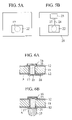
- FIG. 5A and FIG. 5B are plan views showing the semiconductor substrate as seen from the above.
- FIG. 6A and FIG. 6B are schematic cross section views showing the semiconductor substrate obtained by the first embodiment of the manufacturing method in accordance with the present invention.
- FIG. 7A through FIG. 7F are cross sectional views showing a second embodiment of the method of manufacturing a semiconductor device provided with a through hole electrode in accordance with the present invention.
- FIG. 8A and FIG. 8B are plan views showing the semiconductor device as seen from the above.
- FIG. 9A and FIG. 9B are schematic cross section views showing the semiconductor substrate obtained by the manufacturing method in accordance with the present invention.
- FIG. 4A through FIG. 4G are cross sectional views showing a first embodiment of the method of manufacturing a semiconductor substrate provided with a through hole electrode in accordance with the present invention; the views are arranged in the order of manufacturing.
- the cross section is normal to the semiconductor substrate and along the longitudinal direction of the through hole electrode.
- FIG. 5A and FIG. 5B are plan views showing the semiconductor substrate provided with a through hole electrode as seen from the above.
- an interposer which can be used for 3D stacking is manufactured.
- a semiconductor substrate 11 made of a silicon substrate having a thickness of 300 ⁇ m or thereabout is prepared, and a first silicon oxide films 12 (acting as insulating layer) having a thickness of 1 ⁇ m or the like are formed on both the upper and lower surfaces (principal surfaces) of the substrate 11 (a first insulating layer formation step).
- the first silicon oxide film 12 is formed, for example, by thermal oxidation at 1000° C. for four hours.
- the first silicon oxide film 12 can be formed also by a plasma CVD technique, a sputtering technique or the like, instead of thermal oxidation, in accordance with the film thickness of the silicon oxide film and/or the application as desired.
- a silicon substrate is used as the semiconductor substrate 11 , and thus it is possible to easily form the first silicon oxide film 12 as an insulating layer by thermal oxidation or the like.
- the semiconductor substrate 11 is insulated from a thin metal film, which is to be formed in a later step.
- this thin metal film is patterned in accordance with a desired profile, it is possible to make use of this thin metal film as a wiring pattern between the through hole electrode and electric devices to be stacked on the semiconductor substrate 11 .
- the first silicon oxide film 12 functions as an etching stop layer when the small hole is formed by a DRIE technique (as described below), and therefore it is possible to uniformly form the small hole in the surface of the semiconductor substrate 11 .
- the first silicon oxide film 12 can be selectively removed by selecting an appropriate etching gas (as described below).
- the thin metal film (hereinafter described) can serve as an etching stopper layer. As a result, it is possible to form a desired small hole just below the thin metal film by consecutive manufacturing steps.
- the first silicon oxide film 12 on the lower surface A of the substrate 11 is partially removed at a location where the through hole electrode is to be formed.
- a small hole 13 is formed through the semiconductor substrate 11 from the lower surface (principal surface) A to the first silicon oxide film 12 formed on the upper surface (other principal surface) by a deep-reactive ion etching method (in a small hole formation step).
- the deep-reactive ion etching method is performed by alternately performing an etching process with sulfur hexafluoride (SF6) or the like and forming passivation films on the side wall of the small hole 13 (as the Bosch process) in order to deeply etch the semiconductor substrate 11 .
- the cross section of the small hole 13 in the plane perpendicular to the depth direction may have any profile such as a circle, an ellipse, a triangle, a square, a rectangle and so forth and may have any appropriate area or extension depending upon the size, conductivity (resistance) and the like property of the desired semiconductor substrate provided with a through hole electrode.
- a second silicon oxide film 14 having a thickness of 1 ⁇ m or thereabout is formed on the inside surfaces of the small hole 13 (a second insulating layer formation step).
- the second silicon oxide film 14 is formed, for example, by thermal oxidation at 1000° C. for four hours.
- the second silicon oxide film 14 can be formed also by a plasma CVD technique, a sputtering technique or the like, instead of thermal oxidation, in accordance with the film thickness of the silicon oxide film and/or the use application thereof as desired.
- the semiconductor substrate 11 is insulated from a conductive material that is filled into the small hole 13 in a later step.
- a first thin metal film 15 and a second thin metal film 16 made of different materials are formed on the first silicon oxide film 12 at least in a location just above the small hole 13 (a thin film formation step).
- the first thin metal film 15 and the second thin metal film 16 is formed for example by a sputtering technique.
- the first thin metal film 15 is made of an aluminum silicon (Al—Si) thin film while the second thin metal film 16 is made of an aluminum (Al) thin film in this embodiment.
- the first thin metal film 15 and the second thin metal film 16 may be made of other metallic materials.
- the first thin metal film 15 can be formed by suitably selecting the metallic material from among gold, platinum, titanium, silver, copper, bismuth, tin, nickel, chromium, zinc, and other suitable metals and combinations thereof depending upon the type of the conductive material with which the small hole 13 is filled.
- the second thin metal film 16 can be formed by selecting the metallic material from among gold, platinum, titanium, silver, copper, bismuth, tin, nickel, chromium, zinc, and other suitable metals and combinations thereof depending upon the type of the solder bump.
- the thin metal film formed on the semiconductor substrate 11 is a dual layered structure composed of the first thin metal film 15 and the second thin metal film 16 in this embodiment, the present invention is not limited thereto and it is possible to form the thin metal film in a multiple layered structure made of three or more layers of different metals.
- the thin metal film on the semiconductor substrate 11 in a multiple layered structure made of two or more layers of different metals, it is possible to improve the adhesiveness of the thin metal film to the conductive material that fills the small hole 13 and therefore possible to improve the reliability of the electrical connection between the through hole electrode 17 and the thin metal film (the first thin metal film 15 and the second thin metal film 16 in this case).
- the first silicon oxide film 12 is partially removed only at the upper end of the small hole 13 just below the first thin metal film 15 by etching (an insulating layer removing step). Then, the first thin metal film 15 is exposed to the inside of the small hole 13 .
- the first silicon oxide film 12 is etched by an RIE (Reactive Ion Etching) technique (as a dry etching) by the use of carbon tetrafluoride (CF4) (as etchant gas).
- a conductive material is filled into the small hole 13 by a Molten Metal Suction Method or a screen printing method to form a through hole electrode 17 (a conductive material filling step).
- the first thin metal film 15 and the second thin metal film 16 are electrically connected to the through hole electrode 17 .
- a molten metal is filled into the hole by dipping the semiconductor substrate in a molten metal bath in vacuo and then increasing the pressure (decreasing the degree of vacuum or increasing the pressure to the atmospheric pressure).
- the conductive material may be made of a eutectic composition of 80% by weight of gold (Au) and 20% by weight of tin (Sn).
- Au gold
- Sn tin
- the small hole 13 may be filled with the conductive material made of a eutectic composition of 80% by weight of gold and 20% by weight of tin in this embodiment, the present invention is not limited thereto.
- the conductive material can be made of a different composition of a gold-tin alloy, a metal such as tin and indium, or a solder such as a tin-lead base solder, an indium base solder, a tin base solder, a lead base solder, a gold base solder, aluminum base solder and the like.
- a copper (Cu) paste is filled into the small hole 13 .
- the small hole 13 is completely filled with the conductive material through the deep end of the small hole 13 so that the first thin metal film 15 and the second thin metal film 16 are electrically connected to the through hole electrode 17 without fail.
- the small hole 13 may be filled with a copper paste as the conductive material.
- a copper paste as the conductive material.
- Another conductive paste such as a silver paste, a carbon paste, a gold-tin paste and the like can be used as the conductive material.
- an electrode pad 25 and a wiring pattern 26 may be formed on one of the principal surfaces A of the semiconductor substrate obtained by this embodiment. Also as illustrated in FIG. 6B , a metallic bump 27 may be further formed on the electrode pad 25 .
- the opposite surfaces thereof can be electrically connected with each other by means of the through hole electrode 17 so that it is possible to make use of the semiconductor substrate as an interposer 4 which can be used for 3D stacking.
- FIG. 7A to FIG. 7F and FIG. 8A to FIG. 8B a second embodiment of the manufacturing method in accordance with the present invention will be explained.
- a semiconductor device provided with a through hole electrode is manufactured.
- a through hole electrode is formed through a semiconductor substrate on which a general purpose IC chip for driving and controlling MEMS (Micro Electro Mechanical Systems) or other MEMS devices such as a sensor are provided.
- MEMS Micro Electro Mechanical Systems
- FIG. 7A through FIG. 7F are cross sectional views of a semiconductor device showing the method of this embodiment and arranged in order of manufacturing. The cross section is normal to the plane of the semiconductor substrate and along the longitudinal direction of the through hole electrode.
- FIG. 8A and FIG. 8B are plan views showing the semiconductor device provided with a through hole electrode as seen from the above.
- a first silicon oxide film 32 having a thickness of 1 ⁇ m or thereabout is first formed in a position of semiconductor substrate 30 (a first insulating layer formation step); an electronic device 31 is formed on the upper surface (the principal surface) of semiconductor substrate 30 .
- the semiconductor substrate is made of a silicon substrate having a thickness of 300 ⁇ m or thereabout.
- the first silicon oxide film 32 acts as an insulating layer on the upper surface (a principal surface) of the semiconductor substrate 30 .
- the first silicon oxide film 32 is formed, for example, by plasma CVD technique with tetra-ethoxy-silane (TEOS).
- TEOS tetra-ethoxy-silane
- a through hole electrode is formed in the substrate 30 below the film 32 in a later step.
- the first silicon oxide film 32 may be formed also by plasma CVD technique with silane (SiH4) instead of TEOS. Also, it is possible to employ another film formation technique such as a sputtering technique, a thermal oxidation technique or the like to cause no damage to the electronic device 31 during processing.
- a silicon substrate is used as the semiconductor substrate 30 , and therefore it is possible to easily form the first silicon oxide film 32 acting as an insulating layer by a plasma CVD technique or the like.
- a plasma CVD technique or the like.
- by making use of a silicon substrate it is possible to form a small hole to be hereinafter described with precision as required in the surface of the semiconductor substrate 30 by a DRIE technique.
- the first silicon oxide film 32 insulates the semiconductor substrate 30 from a thin metal film, which is to be formed in a later step.
- a thin metal film which is to be formed in a later step.
- the electric devices may be formed by patterning the thin metal film in a desired profile.
- the first silicon oxide film 32 can be used as an etching stop layer when a small hole is formed by a DRIE technique, so that it is possible to uniformly form the small hole in the semiconductor substrate 30 . Further, the first silicon oxide film 32 above the small hole can be selectively removed by selecting an appropriate etching gas as described below. In this case, the thin metal film can serve as an etching stopper layer. Thus it is possible to form a desired small hole just below the thin metal film consecutively.
- a first thin metal film 33 and a second thin metal film 34 of different materials are formed at least on the first silicon oxide film 32 (a thin film formation step).
- the first thin metal film 33 and the second thin metal film 34 are formed for example by a sputtering technique.
- the first thin metal film 33 may be made of an aluminum silicon thin film while the second thin metal film 34 is made of an aluminum thin film.
- an electrode pad 38 and a wiring pattern 39 by pattering the thin metal films; the wiring pattern 39 connects the electronic device 31 and the electrode pad 38 .
- the electrode pad 38 and the wiring pattern 39 may be formed simultaneously.
- the first thin metal film 33 is made of an aluminum silicon thin film while the second thin metal film 34 is made of an aluminum thin film in this embodiment; however, the present invention is not limited thereto.
- the first thin metal film 33 can be formed by suitably selecting the metallic material from among gold, platinum, titanium, silver, copper, bismuth, tin, nickel, chromium, zinc, and other suitable metals and combinations thereof depending upon the type of the conductive material with which a small hole is to be filled.
- the second thin metal film 34 can be formed by selecting the metallic material from among gold, platinum, titanium, silver, copper, bismuth, tin, nickel, chromium, zinc, and other suitable metals and combinations thereof.
- the thin metal film formed on the semiconductor substrate 30 is a dual layered structure composed of the first thin metal film 33 and the second thin metal film 34 in this embodiment, the present invention is not limited thereto so that it is possible to form the thin metal film in a multiple layered structure made of three or more layers of different metals.
- the thin metal film on the semiconductor substrate 30 in a multiple layered structure made of two or more layers of different metals, it is possible to further improve the adhesiveness of the thin metal film to the conductive material with which the small hole is filled and therefore possible to improve the reliability of the electrical connection between the through hole electrode and the thin metal film (the first thin metal film 33 and the second thin metal film 34 in this embodiment).
- a small hole 35 is formed by a DRIE technique from the lower surface (principal surface) B of the semiconductor substrate 30 opposite to the upper surface (principal surface) of the semiconductor substrate 30 where the electronic device 31 and the electrode pad 38 are formed (small hole formation step).
- the small hole 35 is located in a position below the electrode pad 38 and vertically extends to the first silicon oxide film 32 .
- the cross section of the small hole 35 in the plane perpendicular to the depth direction may have any profile such as a circle, an ellipse, a triangle, a square, a rectangle and so forth and may have any appropriate area or extension depending upon the size, conductivity (resistance) and the like property of the desired semiconductor substrate provided with a through hole electrode.
- the DRIE technique it is possible to easily perform microscopic machining of the small hole 35 . Also, by appropriately selecting a semiconductor substrate and an etching gas, forming the small hole 35 and removing a second silicon oxide film just below the thin metal films 33 , 34 can be performed consecutively as described below. Resultantly, the forming the small hole 35 can be made efficiently.
- a second silicon oxide film 36 having a thickness of 1 ⁇ m or thereabout is formed on the lower surface (other principal surface) B of the semiconductor substrate 30 , the inside surface of the small hole 35 and the lower surface of the silicon oxide film 32 (a second insulating layer formation step).
- the second silicon oxide film 36 is formed, for example, by plasma CVD technique with tetra-ethoxy-silane (TEOS).
- the second silicon oxide film 36 can be formed also by plasma CVD technique with silane (SiH4) instead of TEOS. Also, it is possible to employ another film formation technique such as a sputtering technique, a thermal oxidation technique or the like to avoid damages to the electronic device 31 during processing.
- the first and second silicon oxide films 32 , 36 above the small hole 35 are etched and removed so as to expose the first thin metal film 33 to the small hole 35 (an insulating layer removing step).
- an anisotropic etching process is used while protecting the silicon oxide film on the lower surface of the substrate 30 by resist material.
- the first and second silicon oxide films 32 , 36 are etched by an RIE (Reactive Ion Etching) technique (as a dry etching) by the use of carbon tetrafluoride (CF4) (as an etchant gas).
- a conductive material is filled into the small hole 35 by a Molten Metal Suction Method or a screen printing technique in order to form a through hole electrode 37 (a conductive material filling step).
- the first thin metal film 33 and the second thin metal film 34 are electrically connected to the through hole electrode 37 .
- the conductive material may include a eutectic composition of 80% by weight of gold and 20% by weight of tin.
- the small hole 35 may be filled with a copper paste.
- the conductive material is filled by a Molten Metal Suction Method, it is possible to effectively fill the small hole 35 with the conductive material even if the size of the small hole 35 is microscopic. Also, the small hole 35 is completely filled with the conductive material through the deep end of the small hole 35 so that the first thin metal film 33 and the second thin metal film 34 are electrically connected to the through hole electrode 37 without fail.
- the small hole 35 is filled with the conductive material made of a eutectic composition of 80% by weight of gold and 20% by weight of tin in this embodiment of the Molten Metal Suction Method
- the present invention is not limited thereto.
- the conductive material can be made of a different composition of a gold-tin alloy, a metal such as tin and indium, or a solder such as a tin-lead base solder, a tin base solder, a lead base solder, a gold base solder, an indium base solder, aluminum base solder and the like.
- a copper (Cu) paste may be used to fill the small hole 35 .
- Cu copper
- the first thin metal film 33 and the second thin metal film 34 is electrically connected to the through hole electrode 37 without fail, so that the through hole electrode 37 securely serves as an electrode.
- the small hole 35 may be filled with a copper paste as the conductive material.
- a copper paste as the conductive material.
- the present invention is not limited thereto.
- Another conductive paste such as a silver paste, a carbon paste, a gold-tin paste and the like can be used as the conductive material for this purpose.
- an electrode pad 40 and a wiring pattern 41 as illustrated in FIG. 9A may be formed on the lower surface (other principal surface) B of the semiconductor substrate.
- a metallic bump 42 as illustrated in FIG. 9B may be formed on the electrode pad 40 .
- the opposite surfaces are connected to each other by means of the through hole electrode 37 so that it is possible to achieve 3D chip stacking.
- the electronic device 31 and the through hole electrode 37 are electrically connected to each other by patterning the first thin metal film 33 or the second thin metal film 34 to form the electrode pad 38 and the wiring pattern 39 at the same time.
- the present invention is not limited thereto.
- a through hole electrode is efficiently formed through a semiconductor substrate on which an electronic device(s) or a wiring pattern have been fabricated and therefore it is possible to easily manufacture a semiconductor substrate provided with a through hole electrode and a semiconductor device provided with a through hole electrode.
Abstract
Description
Claims (12)
Applications Claiming Priority (2)
| Application Number | Priority Date | Filing Date | Title |
|---|---|---|---|
| JP2002-254858 | 2002-08-30 | ||
| JP2002254858A JP2004095849A (en) | 2002-08-30 | 2002-08-30 | Method for manufacturing semiconductor substrate with through electrode, and method for manufacturing semiconductor device with through electrode |
Publications (2)
| Publication Number | Publication Date |
|---|---|
| US20040043615A1 US20040043615A1 (en) | 2004-03-04 |
| US7022609B2 true US7022609B2 (en) | 2006-04-04 |
Family
ID=31972854
Family Applications (1)
| Application Number | Title | Priority Date | Filing Date |
|---|---|---|---|
| US10/646,757 Active 2024-05-12 US7022609B2 (en) | 2002-08-30 | 2003-08-25 | Manufacturing method of a semiconductor substrate provided with a through hole electrode |
Country Status (2)
| Country | Link |
|---|---|
| US (1) | US7022609B2 (en) |
| JP (1) | JP2004095849A (en) |
Cited By (37)
| Publication number | Priority date | Publication date | Assignee | Title |
|---|---|---|---|---|
| US20050056903A1 (en) * | 2003-08-28 | 2005-03-17 | Satoshi Yamamoto | Semiconductor package and method of manufacturing same |
| US20050280112A1 (en) * | 2004-06-17 | 2005-12-22 | Abbott Donald C | Semiconductor assembly having substrate with electroplated contact pads |
| US20050287783A1 (en) * | 2004-06-29 | 2005-12-29 | Kirby Kyle K | Microelectronic devices and methods for forming interconnects in microelectronic devices |
| US20070111516A1 (en) * | 2004-11-09 | 2007-05-17 | Texas Instruments Incorporated | Semiconductor Assembly Having Substrate with Electroplated Contact Pads |
| US20070259517A1 (en) * | 2004-08-27 | 2007-11-08 | Micron Technology, Inc. | Low temperature methods of forming back side redistribution layers in association with through wafer interconnects |
| US20080050911A1 (en) * | 2006-08-28 | 2008-02-28 | Micron Technology, Inc. | Microfeature workpieces having conductive interconnect structures formed by chemically reactive processes, and associated systems and methods |
| US20080070379A1 (en) * | 2006-09-15 | 2008-03-20 | Oki Electric Industry Co., Ltd. | Method of fabricating semiconductor device |
| US20080258267A1 (en) * | 2005-02-17 | 2008-10-23 | Hiroaki Nakashima | Method of Producing Semiconductor Device and Semiconductor Device |
| US20090008144A1 (en) * | 2004-08-27 | 2009-01-08 | Micron Technology, Inc. | Slanted vias for electrical circuits on circuit boards and other substrates |
| US20090117738A1 (en) * | 2007-10-25 | 2009-05-07 | Shinko Electric Industries Co., Ltd. | Method for producing substrate |
| US20090212008A1 (en) * | 2008-02-27 | 2009-08-27 | Canon Kabushiki Kaisha | Liquid ejection head and manufacturing method thereof |
| US7683458B2 (en) | 2004-09-02 | 2010-03-23 | Micron Technology, Inc. | Through-wafer interconnects for photoimager and memory wafers |
| US7723213B2 (en) * | 2006-11-02 | 2010-05-25 | Oki Semiconductor Co., Ltd. | Manufacturing method of semiconductor chips and semiconductor device having the semiconductor chips |
| US20100154211A1 (en) * | 2008-12-19 | 2010-06-24 | Canon Kabushiki Kaisha | Method for manufacturing wiring board and method for manufacturing inkjet printhead substrate |
| US7749899B2 (en) | 2006-06-01 | 2010-07-06 | Micron Technology, Inc. | Microelectronic workpieces and methods and systems for forming interconnects in microelectronic workpieces |
| US7759800B2 (en) | 2003-11-13 | 2010-07-20 | Micron Technology, Inc. | Microelectronics devices, having vias, and packaged microelectronic devices having vias |
| US7795134B2 (en) | 2005-06-28 | 2010-09-14 | Micron Technology, Inc. | Conductive interconnect structures and formation methods using supercritical fluids |
| US7830018B2 (en) | 2007-08-31 | 2010-11-09 | Micron Technology, Inc. | Partitioned through-layer via and associated systems and methods |
| US7863187B2 (en) | 2005-09-01 | 2011-01-04 | Micron Technology, Inc. | Microfeature workpieces and methods for forming interconnects in microfeature workpieces |
| US7884015B2 (en) | 2007-12-06 | 2011-02-08 | Micron Technology, Inc. | Methods for forming interconnects in microelectronic workpieces and microelectronic workpieces formed using such methods |
| US7902643B2 (en) | 2006-08-31 | 2011-03-08 | Micron Technology, Inc. | Microfeature workpieces having interconnects and conductive backplanes, and associated systems and methods |
| US7915736B2 (en) | 2005-09-01 | 2011-03-29 | Micron Technology, Inc. | Microfeature workpieces and methods for forming interconnects in microfeature workpieces |
| US8084866B2 (en) | 2003-12-10 | 2011-12-27 | Micron Technology, Inc. | Microelectronic devices and methods for filling vias in microelectronic devices |
| US8324511B1 (en) | 2010-04-06 | 2012-12-04 | Amkor Technology, Inc. | Through via nub reveal method and structure |
| US20130040453A1 (en) * | 2008-08-05 | 2013-02-14 | Taiwan Semiconductor Manufacturing Company, Ltd. | Through Silicon Via Layout |
| US8390130B1 (en) | 2011-01-06 | 2013-03-05 | Amkor Technology, Inc. | Through via recessed reveal structure and method |
| US20130099360A1 (en) * | 2011-10-21 | 2013-04-25 | SK Hynix Inc. | Semiconductor package and method for manufacturing the same |
| US8440554B1 (en) * | 2010-08-02 | 2013-05-14 | Amkor Technology, Inc. | Through via connected backside embedded circuit features structure and method |
| US8487445B1 (en) | 2010-10-05 | 2013-07-16 | Amkor Technology, Inc. | Semiconductor device having through electrodes protruding from dielectric layer |
| US8536485B2 (en) | 2004-05-05 | 2013-09-17 | Micron Technology, Inc. | Systems and methods for forming apertures in microfeature workpieces |
| US8552548B1 (en) | 2011-11-29 | 2013-10-08 | Amkor Technology, Inc. | Conductive pad on protruding through electrode semiconductor device |
| US20140284772A1 (en) * | 2013-03-19 | 2014-09-25 | Kabushiki Kaisha Toshiba | Semiconductor device manufacturing method and semiconductor device thereof |
| US20140300002A1 (en) * | 2013-04-08 | 2014-10-09 | Stats Chippac, Ltd. | Semiconductor Device and Method of Forming Conductive Vias Using Backside Via Reveal and Selective Passivation |
| US9048298B1 (en) | 2012-03-29 | 2015-06-02 | Amkor Technology, Inc. | Backside warpage control structure and fabrication method |
| US9129943B1 (en) | 2012-03-29 | 2015-09-08 | Amkor Technology, Inc. | Embedded component package and fabrication method |
| US20150263647A1 (en) * | 2014-03-15 | 2015-09-17 | Canon Kabushiki Kaisha | Device having element electrode connected to penetrating wire, and method for manufacturing the same |
| US9214391B2 (en) | 2004-12-30 | 2015-12-15 | Micron Technology, Inc. | Methods for forming interconnects in microelectronic workpieces and microelectronic workpieces formed using such methods |
Families Citing this family (55)
| Publication number | Priority date | Publication date | Assignee | Title |
|---|---|---|---|---|
| WO2002025630A2 (en) * | 2000-09-20 | 2002-03-28 | Molecular Reflections | Microfabricated ultrasound array for use as resonant sensors |
| WO2005093827A1 (en) * | 2004-03-26 | 2005-10-06 | Fujikura Ltd. | Through wiring board and method for producing the same |
| JP3751625B2 (en) * | 2004-06-29 | 2006-03-01 | 新光電気工業株式会社 | Manufacturing method of through electrode |
| KR100594716B1 (en) * | 2004-07-27 | 2006-06-30 | 삼성전자주식회사 | Cap wafer comprising cavity, semiconductor chip comprising the cap wafer, and method thereof |
| JP4845368B2 (en) * | 2004-10-28 | 2011-12-28 | オンセミコンダクター・トレーディング・リミテッド | Semiconductor device and manufacturing method thereof |
| TW200620451A (en) | 2004-11-09 | 2006-06-16 | Univ Osaka | Method for forming hole in crystal substrate, and crystal substrate having hole formed by the method |
| JP4708009B2 (en) * | 2004-12-14 | 2011-06-22 | 株式会社フジクラ | Wiring board manufacturing method |
| US7611908B2 (en) * | 2005-05-02 | 2009-11-03 | Bioscale, Inc. | Method and apparatus for therapeutic drug monitoring using an acoustic device |
| US7648844B2 (en) * | 2005-05-02 | 2010-01-19 | Bioscale, Inc. | Method and apparatus for detection of analyte using an acoustic device |
| US7300631B2 (en) * | 2005-05-02 | 2007-11-27 | Bioscale, Inc. | Method and apparatus for detection of analyte using a flexural plate wave device and magnetic particles |
| US7749445B2 (en) * | 2005-05-02 | 2010-07-06 | Bioscale, Inc. | Method and apparatus for analyzing bioprocess fluids |
| JP4851163B2 (en) * | 2005-10-31 | 2012-01-11 | オンセミコンダクター・トレーディング・リミテッド | Manufacturing method of semiconductor device |
| DE102005053494A1 (en) * | 2005-11-09 | 2007-05-16 | Fraunhofer Ges Forschung | Process for producing electrically conductive feedthroughs through non-conductive or semiconductive substrates |
| JP4882350B2 (en) * | 2005-11-22 | 2012-02-22 | セイコーエプソン株式会社 | Manufacturing method of semiconductor device |
| US9312217B2 (en) | 2006-02-01 | 2016-04-12 | Silex Microsystems Ab | Methods for making a starting substrate wafer for semiconductor engineering having wafer through connections |
| JP5242063B2 (en) * | 2006-03-22 | 2013-07-24 | 株式会社フジクラ | Wiring board manufacturing method |
| EP2010450A2 (en) * | 2006-04-21 | 2009-01-07 | Bioscale, Inc. | Microfabricated devices and method for fabricating microfabricated devices |
| JP4812512B2 (en) * | 2006-05-19 | 2011-11-09 | オンセミコンダクター・トレーディング・リミテッド | Manufacturing method of semiconductor device |
| JP5103861B2 (en) * | 2006-10-13 | 2012-12-19 | セイコーエプソン株式会社 | SEMICONDUCTOR DEVICE, SEMICONDUCTOR DEVICE MANUFACTURING METHOD, CIRCUIT BOARD AND ELECTRONIC DEVICE |
| US7999440B2 (en) * | 2006-11-27 | 2011-08-16 | Bioscale, Inc. | Micro-fabricated devices having a suspended membrane or plate structure |
| US20080121042A1 (en) * | 2006-11-27 | 2008-05-29 | Bioscale, Inc. | Fluid paths in etchable materials |
| JP4807272B2 (en) * | 2007-02-05 | 2011-11-02 | パナソニック電工株式会社 | Method for forming through-hole wiring on semiconductor wafer |
| KR100843240B1 (en) | 2007-03-23 | 2008-07-03 | 삼성전자주식회사 | Semiconductor device for wafer level stack and forming method of through electrode thereof |
| JP5194537B2 (en) * | 2007-04-23 | 2013-05-08 | 株式会社デンソー | Semiconductor device and manufacturing method thereof |
| US8354280B2 (en) * | 2007-09-06 | 2013-01-15 | Bioscale, Inc. | Reusable detection surfaces and methods of using same |
| JP5343245B2 (en) * | 2008-05-15 | 2013-11-13 | 新光電気工業株式会社 | Manufacturing method of silicon interposer |
| EP2312619A4 (en) * | 2008-08-07 | 2012-12-12 | Fujikura Ltd | Method for manufacturing semiconductor device |
| IT1391239B1 (en) * | 2008-08-08 | 2011-12-01 | Milano Politecnico | METHOD FOR BUMP FORMATION IN SUBSTRATES WITH THROUGH VIA |
| JP5455538B2 (en) * | 2008-10-21 | 2014-03-26 | キヤノン株式会社 | Semiconductor device and manufacturing method thereof |
| KR101026489B1 (en) * | 2009-08-10 | 2011-04-01 | 주식회사 하이닉스반도체 | Semiconductor package and method of manufacturing the same |
| JP5115618B2 (en) | 2009-12-17 | 2013-01-09 | 株式会社デンソー | Semiconductor device |
| WO2011100068A2 (en) * | 2010-02-12 | 2011-08-18 | Eigenlight Corporation | Hermetic package with leaded feedthroughs for in-line fiber optic devices and method of making |
| JP2011243906A (en) | 2010-05-21 | 2011-12-01 | Disco Abrasive Syst Ltd | Method of processing wafer |
| JP5209075B2 (en) | 2010-05-21 | 2013-06-12 | 有限会社 ナプラ | Electronic device and manufacturing method thereof |
| JP5570298B2 (en) * | 2010-05-21 | 2014-08-13 | 株式会社ディスコ | Wafer processing method |
| EP2577724B1 (en) * | 2010-06-03 | 2019-12-11 | Viasystems Technologies Corp., L.L.C. | Method of manufacturing printed circuit board |
| JP2010232685A (en) * | 2010-07-05 | 2010-10-14 | Fujikura Ltd | Method for manufacturing wiring board |
| TWI505348B (en) | 2010-10-08 | 2015-10-21 | Wakom Semiconductor Corp | And a method of forming a microporous structure or a groove structure on the surface of the silicon substrate |
| JP2012099548A (en) * | 2010-10-29 | 2012-05-24 | Fujikura Ltd | Method for manufacturing through wiring board and through wiring board |
| KR101857496B1 (en) * | 2011-10-21 | 2018-05-14 | 에스케이하이닉스 주식회사 | Semiconductor package and method of manufacturing the same |
| JP5994167B2 (en) * | 2011-11-15 | 2016-09-21 | ローム株式会社 | Semiconductor device, manufacturing method thereof, and electronic component |
| JP5998459B2 (en) * | 2011-11-15 | 2016-09-28 | ローム株式会社 | Semiconductor device, manufacturing method thereof, and electronic component |
| US9159699B2 (en) * | 2012-11-13 | 2015-10-13 | Delta Electronics, Inc. | Interconnection structure having a via structure |
| EP2908335B1 (en) * | 2014-02-14 | 2020-04-15 | ams AG | Dicing method |
| JP2015153978A (en) * | 2014-02-18 | 2015-08-24 | キヤノン株式会社 | Manufacturing method of through wiring |
| JP2015187974A (en) * | 2014-03-14 | 2015-10-29 | 日本電子株式会社 | Method of producing sample support film |
| TWI661494B (en) | 2014-07-31 | 2019-06-01 | 美商西凱渥資訊處理科技公司 | Multilayered transient liquid phase bonding |
| JP2016103550A (en) * | 2014-11-28 | 2016-06-02 | キヤノン株式会社 | Electronic device and method of manufacturing the same |
| CN106407881B (en) * | 2015-07-29 | 2020-07-31 | 财团法人工业技术研究院 | Biological identification device and method and wearable carrier |
| JP2017112187A (en) * | 2015-12-15 | 2017-06-22 | キヤノン株式会社 | Device including element provided on board with through wiring and method of manufacturing the same |
| US10965269B2 (en) * | 2016-12-02 | 2021-03-30 | Skyworks Solutions, Inc. | Electronic devices formed in a cavity between substrates and including a via |
| US9941210B1 (en) * | 2016-12-27 | 2018-04-10 | Nxp Usa, Inc. | Semiconductor devices with protruding conductive vias and methods of making such devices |
| JP2018125376A (en) * | 2017-01-31 | 2018-08-09 | 住友精密工業株式会社 | Method for manufacturing wiring structure |
| CN107833859A (en) * | 2017-12-12 | 2018-03-23 | 成都海威华芯科技有限公司 | A kind of Si via metals preparation method |
| US11004779B2 (en) * | 2018-02-09 | 2021-05-11 | Advanced Semiconductor Engineering, Inc. | Semiconductor device package and a method of manufacturing the same |
Citations (6)
| Publication number | Priority date | Publication date | Assignee | Title |
|---|---|---|---|---|
| US5501893A (en) * | 1992-12-05 | 1996-03-26 | Robert Bosch Gmbh | Method of anisotropically etching silicon |
| US6239495B1 (en) * | 1998-07-29 | 2001-05-29 | Kabushiki Kaisha Toshiba | Multichip semiconductor device and memory card |
| US6756681B1 (en) * | 2002-12-23 | 2004-06-29 | Nokia Corporation | Radio frequency integrated circuit having increased substrate resistance enabling three dimensional interconnection with feedthroughs |
| US6790775B2 (en) * | 2002-10-31 | 2004-09-14 | Hewlett-Packard Development Company, L.P. | Method of forming a through-substrate interconnect |
| US6856210B2 (en) * | 2000-04-27 | 2005-02-15 | Sharp Kabushiki Kaisha | High-frequency multilayer circuit substrate |
| US6864172B2 (en) * | 2002-06-18 | 2005-03-08 | Sanyo Electric Co., Ltd. | Manufacturing method of semiconductor device |
Family Cites Families (15)
| Publication number | Priority date | Publication date | Assignee | Title |
|---|---|---|---|---|
| JPS63156348A (en) * | 1986-12-19 | 1988-06-29 | Fujitsu Ltd | Semiconductor device |
| JPH04133472A (en) * | 1990-09-26 | 1992-05-07 | Toshiba Corp | Compound semiconductor device and manufacture thereof |
| JP2000243906A (en) * | 1999-02-18 | 2000-09-08 | Sharp Corp | Semiconductor device and manufacture thereof |
| US6617681B1 (en) * | 1999-06-28 | 2003-09-09 | Intel Corporation | Interposer and method of making same |
| JP3687435B2 (en) * | 1999-08-27 | 2005-08-24 | セイコーエプソン株式会社 | Semiconductor chip and manufacturing method thereof, semiconductor device, computer, circuit board, and electronic device |
| US6694321B1 (en) * | 1999-09-23 | 2004-02-17 | Affymetrix, Inc. | System, method, and product for development and maintenance of database-related software applications |
| JP2002057271A (en) * | 2000-08-10 | 2002-02-22 | Matsushita Electric Ind Co Ltd | Semiconductor and its fabricating method |
| US6402301B1 (en) * | 2000-10-27 | 2002-06-11 | Lexmark International, Inc | Ink jet printheads and methods therefor |
| JP3627856B2 (en) * | 2000-11-22 | 2005-03-09 | 株式会社フジクラ | Metal filling apparatus and metal filling method for fine space |
| JP3535461B2 (en) * | 2001-01-10 | 2004-06-07 | 新光電気工業株式会社 | Semiconductor device manufacturing method and semiconductor device |
| JP3599325B2 (en) * | 2001-02-09 | 2004-12-08 | 株式会社フジクラ | Method of forming through electrode on substrate and substrate having through electrode |
| US20030101190A1 (en) * | 2001-03-14 | 2003-05-29 | Microsoft Corporation | Schema-based notification service |
| US6810516B2 (en) * | 2001-10-30 | 2004-10-26 | Hewlett-Packard Development Company, L.P. | Mechanism allowing separation of graphical display of object status from underlying data |
| US6952704B2 (en) * | 2001-11-26 | 2005-10-04 | Microsoft Corporation | Extending a directory schema independent of schema modification |
| US7206788B2 (en) * | 2002-07-30 | 2007-04-17 | Microsoft Corporation | Schema-based services for identity-based access to device data |
-
2002
- 2002-08-30 JP JP2002254858A patent/JP2004095849A/en active Pending
-
2003
- 2003-08-25 US US10/646,757 patent/US7022609B2/en active Active
Patent Citations (6)
| Publication number | Priority date | Publication date | Assignee | Title |
|---|---|---|---|---|
| US5501893A (en) * | 1992-12-05 | 1996-03-26 | Robert Bosch Gmbh | Method of anisotropically etching silicon |
| US6239495B1 (en) * | 1998-07-29 | 2001-05-29 | Kabushiki Kaisha Toshiba | Multichip semiconductor device and memory card |
| US6856210B2 (en) * | 2000-04-27 | 2005-02-15 | Sharp Kabushiki Kaisha | High-frequency multilayer circuit substrate |
| US6864172B2 (en) * | 2002-06-18 | 2005-03-08 | Sanyo Electric Co., Ltd. | Manufacturing method of semiconductor device |
| US6790775B2 (en) * | 2002-10-31 | 2004-09-14 | Hewlett-Packard Development Company, L.P. | Method of forming a through-substrate interconnect |
| US6756681B1 (en) * | 2002-12-23 | 2004-06-29 | Nokia Corporation | Radio frequency integrated circuit having increased substrate resistance enabling three dimensional interconnection with feedthroughs |
Cited By (92)
| Publication number | Priority date | Publication date | Assignee | Title |
|---|---|---|---|---|
| AU2004268299B2 (en) * | 2003-08-28 | 2009-05-21 | Olympus Corporation | Semiconductor package and manufacturing method thereof |
| US20050056903A1 (en) * | 2003-08-28 | 2005-03-17 | Satoshi Yamamoto | Semiconductor package and method of manufacturing same |
| US7180149B2 (en) * | 2003-08-28 | 2007-02-20 | Fujikura Ltd. | Semiconductor package with through-hole |
| US7759800B2 (en) | 2003-11-13 | 2010-07-20 | Micron Technology, Inc. | Microelectronics devices, having vias, and packaged microelectronic devices having vias |
| US9653420B2 (en) | 2003-11-13 | 2017-05-16 | Micron Technology, Inc. | Microelectronic devices and methods for filling vias in microelectronic devices |
| US8084866B2 (en) | 2003-12-10 | 2011-12-27 | Micron Technology, Inc. | Microelectronic devices and methods for filling vias in microelectronic devices |
| US11177175B2 (en) | 2003-12-10 | 2021-11-16 | Micron Technology, Inc. | Microelectronic devices and methods for filling vias in microelectronic devices |
| US8748311B2 (en) | 2003-12-10 | 2014-06-10 | Micron Technology, Inc. | Microelectronic devices and methods for filing vias in microelectronic devices |
| US8664562B2 (en) | 2004-05-05 | 2014-03-04 | Micron Technology, Inc. | Systems and methods for forming apertures in microfeature workpieces |
| US8686313B2 (en) | 2004-05-05 | 2014-04-01 | Micron Technology, Inc. | System and methods for forming apertures in microfeature workpieces |
| US8536485B2 (en) | 2004-05-05 | 2013-09-17 | Micron Technology, Inc. | Systems and methods for forming apertures in microfeature workpieces |
| US9452492B2 (en) | 2004-05-05 | 2016-09-27 | Micron Technology, Inc. | Systems and methods for forming apertures in microfeature workpieces |
| US10010977B2 (en) | 2004-05-05 | 2018-07-03 | Micron Technology, Inc. | Systems and methods for forming apertures in microfeature workpieces |
| US7179738B2 (en) * | 2004-06-17 | 2007-02-20 | Texas Instruments Incorporated | Semiconductor assembly having substrate with electroplated contact pads |
| US20050280112A1 (en) * | 2004-06-17 | 2005-12-22 | Abbott Donald C | Semiconductor assembly having substrate with electroplated contact pads |
| US7329943B2 (en) * | 2004-06-29 | 2008-02-12 | Micron Technology, Inc. | Microelectronic devices and methods for forming interconnects in microelectronic devices |
| US20080138973A1 (en) * | 2004-06-29 | 2008-06-12 | Micron Technology, Inc. | Microelectronic devices and methods for forming interconnects in microelectronic devices |
| US7232754B2 (en) * | 2004-06-29 | 2007-06-19 | Micron Technology, Inc. | Microelectronic devices and methods for forming interconnects in microelectronic devices |
| US20060199363A1 (en) * | 2004-06-29 | 2006-09-07 | Micron Technology, Inc. | Microelectronic devices and methods for forming interconnects in microelectronic devices |
| US20050287783A1 (en) * | 2004-06-29 | 2005-12-29 | Kirby Kyle K | Microelectronic devices and methods for forming interconnects in microelectronic devices |
| US7829976B2 (en) | 2004-06-29 | 2010-11-09 | Micron Technology, Inc. | Microelectronic devices and methods for forming interconnects in microelectronic devices |
| US8322031B2 (en) | 2004-08-27 | 2012-12-04 | Micron Technology, Inc. | Method of manufacturing an interposer |
| US7419852B2 (en) | 2004-08-27 | 2008-09-02 | Micron Technology, Inc. | Low temperature methods of forming back side redistribution layers in association with through wafer interconnects, semiconductor devices including same, and assemblies |
| US7435620B2 (en) * | 2004-08-27 | 2008-10-14 | Micron Technology, Inc. | Low temperature methods of forming back side redistribution layers in association with through wafer interconnects |
| US7994547B2 (en) * | 2004-08-27 | 2011-08-09 | Micron Technology, Inc. | Semiconductor devices and assemblies including back side redistribution layers in association with through wafer interconnects |
| US20080277799A1 (en) * | 2004-08-27 | 2008-11-13 | Micron Technology, Inc. | Low temperature methods of forming back side redistribution layers in association with through wafer interconnects, semiconductor devices including same, and assemblies |
| US20070259517A1 (en) * | 2004-08-27 | 2007-11-08 | Micron Technology, Inc. | Low temperature methods of forming back side redistribution layers in association with through wafer interconnects |
| US20090008144A1 (en) * | 2004-08-27 | 2009-01-08 | Micron Technology, Inc. | Slanted vias for electrical circuits on circuit boards and other substrates |
| US7683458B2 (en) | 2004-09-02 | 2010-03-23 | Micron Technology, Inc. | Through-wafer interconnects for photoimager and memory wafers |
| US7956443B2 (en) | 2004-09-02 | 2011-06-07 | Micron Technology, Inc. | Through-wafer interconnects for photoimager and memory wafers |
| US8669179B2 (en) | 2004-09-02 | 2014-03-11 | Micron Technology, Inc. | Through-wafer interconnects for photoimager and memory wafers |
| US8502353B2 (en) | 2004-09-02 | 2013-08-06 | Micron Technology, Inc. | Through-wafer interconnects for photoimager and memory wafers |
| US7411303B2 (en) | 2004-11-09 | 2008-08-12 | Texas Instruments Incorporated | Semiconductor assembly having substrate with electroplated contact pads |
| US20070111516A1 (en) * | 2004-11-09 | 2007-05-17 | Texas Instruments Incorporated | Semiconductor Assembly Having Substrate with Electroplated Contact Pads |
| US9214391B2 (en) | 2004-12-30 | 2015-12-15 | Micron Technology, Inc. | Methods for forming interconnects in microelectronic workpieces and microelectronic workpieces formed using such methods |
| US8278738B2 (en) * | 2005-02-17 | 2012-10-02 | Sharp Kabushiki Kaisha | Method of producing semiconductor device and semiconductor device |
| US20080258267A1 (en) * | 2005-02-17 | 2008-10-23 | Hiroaki Nakashima | Method of Producing Semiconductor Device and Semiconductor Device |
| US9293367B2 (en) | 2005-06-28 | 2016-03-22 | Micron Technology, Inc. | Conductive interconnect structures and formation methods using supercritical fluids |
| US8008192B2 (en) | 2005-06-28 | 2011-08-30 | Micron Technology, Inc. | Conductive interconnect structures and formation methods using supercritical fluids |
| US7795134B2 (en) | 2005-06-28 | 2010-09-14 | Micron Technology, Inc. | Conductive interconnect structures and formation methods using supercritical fluids |
| US7863187B2 (en) | 2005-09-01 | 2011-01-04 | Micron Technology, Inc. | Microfeature workpieces and methods for forming interconnects in microfeature workpieces |
| US7915736B2 (en) | 2005-09-01 | 2011-03-29 | Micron Technology, Inc. | Microfeature workpieces and methods for forming interconnects in microfeature workpieces |
| US11476160B2 (en) | 2005-09-01 | 2022-10-18 | Micron Technology, Inc. | Microfeature workpieces and methods for forming interconnects in microfeature workpieces |
| US7749899B2 (en) | 2006-06-01 | 2010-07-06 | Micron Technology, Inc. | Microelectronic workpieces and methods and systems for forming interconnects in microelectronic workpieces |
| US20080050911A1 (en) * | 2006-08-28 | 2008-02-28 | Micron Technology, Inc. | Microfeature workpieces having conductive interconnect structures formed by chemically reactive processes, and associated systems and methods |
| US7973411B2 (en) | 2006-08-28 | 2011-07-05 | Micron Technology, Inc. | Microfeature workpieces having conductive interconnect structures formed by chemically reactive processes, and associated systems and methods |
| US8610279B2 (en) | 2006-08-28 | 2013-12-17 | Micron Technologies, Inc. | Microfeature workpieces having conductive interconnect structures formed by chemically reactive processes, and associated systems and methods |
| US9570350B2 (en) | 2006-08-31 | 2017-02-14 | Micron Technology, Inc. | Microfeature workpieces having interconnects and conductive backplanes, and associated systems and methods |
| US9099539B2 (en) | 2006-08-31 | 2015-08-04 | Micron Technology, Inc. | Microfeature workpieces having interconnects and conductive backplanes, and associated systems and methods |
| US7902643B2 (en) | 2006-08-31 | 2011-03-08 | Micron Technology, Inc. | Microfeature workpieces having interconnects and conductive backplanes, and associated systems and methods |
| US8178421B2 (en) | 2006-09-15 | 2012-05-15 | Oki Semiconductor Co., Ltd. | Method of fabricating semiconductor device |
| US20080070379A1 (en) * | 2006-09-15 | 2008-03-20 | Oki Electric Industry Co., Ltd. | Method of fabricating semiconductor device |
| US7723213B2 (en) * | 2006-11-02 | 2010-05-25 | Oki Semiconductor Co., Ltd. | Manufacturing method of semiconductor chips and semiconductor device having the semiconductor chips |
| US8367538B2 (en) | 2007-08-31 | 2013-02-05 | Micron Technology, Inc. | Partitioned through-layer via and associated systems and methods |
| US8536046B2 (en) | 2007-08-31 | 2013-09-17 | Micron Technology | Partitioned through-layer via and associated systems and methods |
| US7830018B2 (en) | 2007-08-31 | 2010-11-09 | Micron Technology, Inc. | Partitioned through-layer via and associated systems and methods |
| US7867894B2 (en) * | 2007-10-25 | 2011-01-11 | Shinko Electric Industries Co., Ltd. | Method for producing substrate |
| US20090117738A1 (en) * | 2007-10-25 | 2009-05-07 | Shinko Electric Industries Co., Ltd. | Method for producing substrate |
| US7884015B2 (en) | 2007-12-06 | 2011-02-08 | Micron Technology, Inc. | Methods for forming interconnects in microelectronic workpieces and microelectronic workpieces formed using such methods |
| US9281241B2 (en) | 2007-12-06 | 2016-03-08 | Micron Technology, Inc. | Methods for forming interconnects in microelectronic workpieces and microelectronic workpieces formed using such methods |
| US8247907B2 (en) | 2007-12-06 | 2012-08-21 | Micron Technology, Inc. | Methods for forming interconnects in microelectronic workpieces and microelectronic workpieces formed using such methods |
| US8205967B2 (en) | 2008-02-27 | 2012-06-26 | Canon Kabushiki Kaisha | Liquid ejection head and manufacturing method thereof |
| US20090212008A1 (en) * | 2008-02-27 | 2009-08-27 | Canon Kabushiki Kaisha | Liquid ejection head and manufacturing method thereof |
| US20130040453A1 (en) * | 2008-08-05 | 2013-02-14 | Taiwan Semiconductor Manufacturing Company, Ltd. | Through Silicon Via Layout |
| US8716131B2 (en) * | 2008-08-05 | 2014-05-06 | Taiwan Semiconductor Manufacturing Company, Ltd. | Through silicon via layout |
| US20100154211A1 (en) * | 2008-12-19 | 2010-06-24 | Canon Kabushiki Kaisha | Method for manufacturing wiring board and method for manufacturing inkjet printhead substrate |
| US8448333B2 (en) | 2008-12-19 | 2013-05-28 | Canon Kabushiki Kaisha | Method for manufacturing wiring board and method for manufacturing inkjet printhead substrate |
| US8324511B1 (en) | 2010-04-06 | 2012-12-04 | Amkor Technology, Inc. | Through via nub reveal method and structure |
| US9324614B1 (en) | 2010-04-06 | 2016-04-26 | Amkor Technology, Inc. | Through via nub reveal method and structure |
| US9159672B1 (en) | 2010-08-02 | 2015-10-13 | Amkor Technology, Inc. | Through via connected backside embedded circuit features structure and method |
| US8440554B1 (en) * | 2010-08-02 | 2013-05-14 | Amkor Technology, Inc. | Through via connected backside embedded circuit features structure and method |
| US8900995B1 (en) | 2010-10-05 | 2014-12-02 | Amkor Technology, Inc. | Semiconductor device and manufacturing method thereof |
| US8487445B1 (en) | 2010-10-05 | 2013-07-16 | Amkor Technology, Inc. | Semiconductor device having through electrodes protruding from dielectric layer |
| US8390130B1 (en) | 2011-01-06 | 2013-03-05 | Amkor Technology, Inc. | Through via recessed reveal structure and method |
| US9082833B1 (en) | 2011-01-06 | 2015-07-14 | Amkor Technology, Inc. | Through via recessed reveal structure and method |
| US20130099360A1 (en) * | 2011-10-21 | 2013-04-25 | SK Hynix Inc. | Semiconductor package and method for manufacturing the same |
| US9040419B2 (en) * | 2011-10-21 | 2015-05-26 | SK Hynix Inc. | Semiconductor package and method for manufacturing the same |
| US8816477B2 (en) * | 2011-10-21 | 2014-08-26 | SK Hynix Inc. | Semiconductor package having a contamination preventing layer formed in the semiconductor chip |
| US10410967B1 (en) | 2011-11-29 | 2019-09-10 | Amkor Technology, Inc. | Electronic device comprising a conductive pad on a protruding-through electrode |
| US8552548B1 (en) | 2011-11-29 | 2013-10-08 | Amkor Technology, Inc. | Conductive pad on protruding through electrode semiconductor device |
| US9947623B1 (en) | 2011-11-29 | 2018-04-17 | Amkor Technology, Inc. | Semiconductor device comprising a conductive pad on a protruding-through electrode |
| US8981572B1 (en) | 2011-11-29 | 2015-03-17 | Amkor Technology, Inc. | Conductive pad on protruding through electrode semiconductor device |
| US9431323B1 (en) | 2011-11-29 | 2016-08-30 | Amkor Technology, Inc. | Conductive pad on protruding through electrode |
| US11043458B2 (en) | 2011-11-29 | 2021-06-22 | Amkor Technology Singapore Holding Pte. Ltd. | Method of manufacturing an electronic device comprising a conductive pad on a protruding-through electrode |
| US9048298B1 (en) | 2012-03-29 | 2015-06-02 | Amkor Technology, Inc. | Backside warpage control structure and fabrication method |
| US9129943B1 (en) | 2012-03-29 | 2015-09-08 | Amkor Technology, Inc. | Embedded component package and fabrication method |
| US10014240B1 (en) | 2012-03-29 | 2018-07-03 | Amkor Technology, Inc. | Embedded component package and fabrication method |
| US20140284772A1 (en) * | 2013-03-19 | 2014-09-25 | Kabushiki Kaisha Toshiba | Semiconductor device manufacturing method and semiconductor device thereof |
| US9865524B2 (en) * | 2013-04-08 | 2018-01-09 | STATS ChipPAC Pte. Ltd. | Semiconductor device and method of forming conductive vias using backside via reveal and selective passivation |
| US20140300002A1 (en) * | 2013-04-08 | 2014-10-09 | Stats Chippac, Ltd. | Semiconductor Device and Method of Forming Conductive Vias Using Backside Via Reveal and Selective Passivation |
| US10073064B2 (en) * | 2014-03-15 | 2018-09-11 | Canon Kabushiki Kaisha | Device having element electrode connected to penetrating wire, and method for manufacturing the same |
| US20150263647A1 (en) * | 2014-03-15 | 2015-09-17 | Canon Kabushiki Kaisha | Device having element electrode connected to penetrating wire, and method for manufacturing the same |
Also Published As
| Publication number | Publication date |
|---|---|
| JP2004095849A (en) | 2004-03-25 |
| US20040043615A1 (en) | 2004-03-04 |
Similar Documents
| Publication | Publication Date | Title |
|---|---|---|
| US7022609B2 (en) | Manufacturing method of a semiconductor substrate provided with a through hole electrode | |
| KR100838440B1 (en) | Electronic device substrate, electronic device and methods for making same | |
| KR100543481B1 (en) | Semiconductor device and manufacturing method thereof | |
| US6611052B2 (en) | Wafer level stackable semiconductor package | |
| US6852621B2 (en) | Semiconductor device and manufacturing method therefor, circuit board, and electronic equipment | |
| KR100831405B1 (en) | Wafer bonding packaging method | |
| TWI387065B (en) | Electronic device packages and methods of formation | |
| JP5021003B2 (en) | High reliability multilayer circuit board and method for forming the same | |
| JP4694305B2 (en) | Manufacturing method of semiconductor wafer | |
| US6235554B1 (en) | Method for fabricating stackable chip scale semiconductor package | |
| KR100840502B1 (en) | Semiconductor device and manufacturing mathod thereof | |
| US7342320B2 (en) | Electronic component with semiconductor chips, electronic assembly composed of stacked semiconductor chips, and methods for producing an electronic component and an electronic assembly | |
| US7745924B2 (en) | Capacitor embedded in interposer, semiconductor device including the same, and method for manufacturing capacitor embedded in interposer | |
| JP4469181B2 (en) | Electronic device and method of manufacturing the same | |
| US8178957B2 (en) | Electronic component device, and method of manufacturing the same | |
| JP2005175019A (en) | Semiconductor device and multilayer semiconductor device | |
| TWI397161B (en) | Integrated circuit having bond pad with improved thermal and mechanical properties | |
| KR20060041997A (en) | Semiconductor device and manufacturing method thereof | |
| KR100754557B1 (en) | Manufacturing method of electronic device | |
| WO2011125935A1 (en) | Semiconductor device and manufacturing method thereof | |
| EP1659092B1 (en) | Method for fabricating an electrode in a packaging substrate | |
| JP5026025B2 (en) | Semiconductor device | |
| JP4401330B2 (en) | Semiconductor device and manufacturing method thereof | |
| JP2009111433A (en) | Manufacturing method of semiconductor substrate with penetrating electrode, and manufacturing method of semiconductor device with penetrating electrode | |
| CN112490197A (en) | Semiconductor device package and method of manufacturing the same |
Legal Events
| Date | Code | Title | Description |
|---|---|---|---|
| AS | Assignment |
Owner name: OLYMPUS OPTICAL CO., LTD., JAPAN Free format text: ASSIGNMENT OF ASSIGNORS INTEREST;ASSIGNORS:YAMAMOTO, SATOSHI;TAKIZAWA, TAKASHI;SUEMASU, TATSUO;AND OTHERS;REEL/FRAME:015097/0736;SIGNING DATES FROM 20030731 TO 20030804 Owner name: FUJIKURA LTD., JAPAN Free format text: ASSIGNMENT OF ASSIGNORS INTEREST;ASSIGNORS:YAMAMOTO, SATOSHI;TAKIZAWA, TAKASHI;SUEMASU, TATSUO;AND OTHERS;REEL/FRAME:015097/0736;SIGNING DATES FROM 20030731 TO 20030804 |
|
| STCF | Information on status: patent grant |
Free format text: PATENTED CASE |
|
| AS | Assignment |
Owner name: OLYMPUS CORPORATION, JAPAN Free format text: CHANGE OF NAME;ASSIGNOR:OLYMPUS OPTICAL CO., LTD.;REEL/FRAME:017627/0674 Effective date: 20031001 |
|
| FEPP | Fee payment procedure |
Free format text: PAYOR NUMBER ASSIGNED (ORIGINAL EVENT CODE: ASPN); ENTITY STATUS OF PATENT OWNER: LARGE ENTITY |
|
| FPAY | Fee payment |
Year of fee payment: 4 |
|
| FPAY | Fee payment |
Year of fee payment: 8 |
|
| AS | Assignment |
Owner name: OLYMPUS CORPORATION, JAPAN Free format text: CHANGE OF ADDRESS;ASSIGNOR:OLYMPUS CORPORATION;REEL/FRAME:039344/0502 Effective date: 20160401 |
|
| MAFP | Maintenance fee payment |
Free format text: PAYMENT OF MAINTENANCE FEE, 12TH YEAR, LARGE ENTITY (ORIGINAL EVENT CODE: M1553) Year of fee payment: 12 |