US6924171B2 - Bilayer wafer-level underfill - Google Patents
Bilayer wafer-level underfill Download PDFInfo
- Publication number
- US6924171B2 US6924171B2 US09/782,494 US78249401A US6924171B2 US 6924171 B2 US6924171 B2 US 6924171B2 US 78249401 A US78249401 A US 78249401A US 6924171 B2 US6924171 B2 US 6924171B2
- Authority
- US
- United States
- Prior art keywords
- polymeric material
- conductive bump
- forming
- wafer
- polymeric
- Prior art date
- Legal status (The legal status is an assumption and is not a legal conclusion. Google has not performed a legal analysis and makes no representation as to the accuracy of the status listed.)
- Expired - Lifetime
Links
Images


Classifications
-
- H—ELECTRICITY
- H01—ELECTRIC ELEMENTS
- H01L—SEMICONDUCTOR DEVICES NOT COVERED BY CLASS H10
- H01L24/00—Arrangements for connecting or disconnecting semiconductor or solid-state bodies; Methods or apparatus related thereto
- H01L24/01—Means for bonding being attached to, or being formed on, the surface to be connected, e.g. chip-to-package, die-attach, "first-level" interconnects; Manufacturing methods related thereto
- H01L24/26—Layer connectors, e.g. plate connectors, solder or adhesive layers; Manufacturing methods related thereto
- H01L24/27—Manufacturing methods
-
- H—ELECTRICITY
- H01—ELECTRIC ELEMENTS
- H01L—SEMICONDUCTOR DEVICES NOT COVERED BY CLASS H10
- H01L21/00—Processes or apparatus adapted for the manufacture or treatment of semiconductor or solid state devices or of parts thereof
- H01L21/02—Manufacture or treatment of semiconductor devices or of parts thereof
- H01L21/04—Manufacture or treatment of semiconductor devices or of parts thereof the devices having at least one potential-jump barrier or surface barrier, e.g. PN junction, depletion layer or carrier concentration layer
- H01L21/50—Assembly of semiconductor devices using processes or apparatus not provided for in a single one of the subgroups H01L21/06 - H01L21/326, e.g. sealing of a cap to a base of a container
- H01L21/56—Encapsulations, e.g. encapsulation layers, coatings
- H01L21/563—Encapsulation of active face of flip-chip device, e.g. underfilling or underencapsulation of flip-chip, encapsulation preform on chip or mounting substrate
-
- H—ELECTRICITY
- H01—ELECTRIC ELEMENTS
- H01L—SEMICONDUCTOR DEVICES NOT COVERED BY CLASS H10
- H01L23/00—Details of semiconductor or other solid state devices
- H01L23/28—Encapsulations, e.g. encapsulating layers, coatings, e.g. for protection
- H01L23/29—Encapsulations, e.g. encapsulating layers, coatings, e.g. for protection characterised by the material, e.g. carbon
- H01L23/293—Organic, e.g. plastic
- H01L23/295—Organic, e.g. plastic containing a filler
-
- H—ELECTRICITY
- H01—ELECTRIC ELEMENTS
- H01L—SEMICONDUCTOR DEVICES NOT COVERED BY CLASS H10
- H01L24/00—Arrangements for connecting or disconnecting semiconductor or solid-state bodies; Methods or apparatus related thereto
- H01L24/01—Means for bonding being attached to, or being formed on, the surface to be connected, e.g. chip-to-package, die-attach, "first-level" interconnects; Manufacturing methods related thereto
- H01L24/10—Bump connectors ; Manufacturing methods related thereto
- H01L24/11—Manufacturing methods
-
- H—ELECTRICITY
- H01—ELECTRIC ELEMENTS
- H01L—SEMICONDUCTOR DEVICES NOT COVERED BY CLASS H10
- H01L24/00—Arrangements for connecting or disconnecting semiconductor or solid-state bodies; Methods or apparatus related thereto
- H01L24/01—Means for bonding being attached to, or being formed on, the surface to be connected, e.g. chip-to-package, die-attach, "first-level" interconnects; Manufacturing methods related thereto
- H01L24/26—Layer connectors, e.g. plate connectors, solder or adhesive layers; Manufacturing methods related thereto
- H01L24/28—Structure, shape, material or disposition of the layer connectors prior to the connecting process
- H01L24/29—Structure, shape, material or disposition of the layer connectors prior to the connecting process of an individual layer connector
-
- H—ELECTRICITY
- H01—ELECTRIC ELEMENTS
- H01L—SEMICONDUCTOR DEVICES NOT COVERED BY CLASS H10
- H01L24/00—Arrangements for connecting or disconnecting semiconductor or solid-state bodies; Methods or apparatus related thereto
- H01L24/93—Batch processes
- H01L24/94—Batch processes at wafer-level, i.e. with connecting carried out on a wafer comprising a plurality of undiced individual devices
-
- H—ELECTRICITY
- H01—ELECTRIC ELEMENTS
- H01L—SEMICONDUCTOR DEVICES NOT COVERED BY CLASS H10
- H01L2224/00—Indexing scheme for arrangements for connecting or disconnecting semiconductor or solid-state bodies and methods related thereto as covered by H01L24/00
- H01L2224/01—Means for bonding being attached to, or being formed on, the surface to be connected, e.g. chip-to-package, die-attach, "first-level" interconnects; Manufacturing methods related thereto
- H01L2224/02—Bonding areas; Manufacturing methods related thereto
- H01L2224/04—Structure, shape, material or disposition of the bonding areas prior to the connecting process
- H01L2224/05—Structure, shape, material or disposition of the bonding areas prior to the connecting process of an individual bonding area
- H01L2224/0554—External layer
- H01L2224/0556—Disposition
- H01L2224/05571—Disposition the external layer being disposed in a recess of the surface
-
- H—ELECTRICITY
- H01—ELECTRIC ELEMENTS
- H01L—SEMICONDUCTOR DEVICES NOT COVERED BY CLASS H10
- H01L2224/00—Indexing scheme for arrangements for connecting or disconnecting semiconductor or solid-state bodies and methods related thereto as covered by H01L24/00
- H01L2224/01—Means for bonding being attached to, or being formed on, the surface to be connected, e.g. chip-to-package, die-attach, "first-level" interconnects; Manufacturing methods related thereto
- H01L2224/02—Bonding areas; Manufacturing methods related thereto
- H01L2224/04—Structure, shape, material or disposition of the bonding areas prior to the connecting process
- H01L2224/05—Structure, shape, material or disposition of the bonding areas prior to the connecting process of an individual bonding area
- H01L2224/0554—External layer
- H01L2224/05573—Single external layer
-
- H—ELECTRICITY
- H01—ELECTRIC ELEMENTS
- H01L—SEMICONDUCTOR DEVICES NOT COVERED BY CLASS H10
- H01L2224/00—Indexing scheme for arrangements for connecting or disconnecting semiconductor or solid-state bodies and methods related thereto as covered by H01L24/00
- H01L2224/01—Means for bonding being attached to, or being formed on, the surface to be connected, e.g. chip-to-package, die-attach, "first-level" interconnects; Manufacturing methods related thereto
- H01L2224/10—Bump connectors; Manufacturing methods related thereto
- H01L2224/11—Manufacturing methods
- H01L2224/1147—Manufacturing methods using a lift-off mask
-
- H—ELECTRICITY
- H01—ELECTRIC ELEMENTS
- H01L—SEMICONDUCTOR DEVICES NOT COVERED BY CLASS H10
- H01L2224/00—Indexing scheme for arrangements for connecting or disconnecting semiconductor or solid-state bodies and methods related thereto as covered by H01L24/00
- H01L2224/01—Means for bonding being attached to, or being formed on, the surface to be connected, e.g. chip-to-package, die-attach, "first-level" interconnects; Manufacturing methods related thereto
- H01L2224/10—Bump connectors; Manufacturing methods related thereto
- H01L2224/12—Structure, shape, material or disposition of the bump connectors prior to the connecting process
- H01L2224/13—Structure, shape, material or disposition of the bump connectors prior to the connecting process of an individual bump connector
- H01L2224/13001—Core members of the bump connector
- H01L2224/13099—Material
- H01L2224/131—Material with a principal constituent of the material being a metal or a metalloid, e.g. boron [B], silicon [Si], germanium [Ge], arsenic [As], antimony [Sb], tellurium [Te] and polonium [Po], and alloys thereof
- H01L2224/13101—Material with a principal constituent of the material being a metal or a metalloid, e.g. boron [B], silicon [Si], germanium [Ge], arsenic [As], antimony [Sb], tellurium [Te] and polonium [Po], and alloys thereof the principal constituent melting at a temperature of less than 400°C
- H01L2224/13111—Tin [Sn] as principal constituent
-
- H—ELECTRICITY
- H01—ELECTRIC ELEMENTS
- H01L—SEMICONDUCTOR DEVICES NOT COVERED BY CLASS H10
- H01L2224/00—Indexing scheme for arrangements for connecting or disconnecting semiconductor or solid-state bodies and methods related thereto as covered by H01L24/00
- H01L2224/01—Means for bonding being attached to, or being formed on, the surface to be connected, e.g. chip-to-package, die-attach, "first-level" interconnects; Manufacturing methods related thereto
- H01L2224/10—Bump connectors; Manufacturing methods related thereto
- H01L2224/15—Structure, shape, material or disposition of the bump connectors after the connecting process
- H01L2224/16—Structure, shape, material or disposition of the bump connectors after the connecting process of an individual bump connector
- H01L2224/161—Disposition
- H01L2224/16151—Disposition the bump connector connecting between a semiconductor or solid-state body and an item not being a semiconductor or solid-state body, e.g. chip-to-substrate, chip-to-passive
- H01L2224/16221—Disposition the bump connector connecting between a semiconductor or solid-state body and an item not being a semiconductor or solid-state body, e.g. chip-to-substrate, chip-to-passive the body and the item being stacked
- H01L2224/16225—Disposition the bump connector connecting between a semiconductor or solid-state body and an item not being a semiconductor or solid-state body, e.g. chip-to-substrate, chip-to-passive the body and the item being stacked the item being non-metallic, e.g. insulating substrate with or without metallisation
-
- H—ELECTRICITY
- H01—ELECTRIC ELEMENTS
- H01L—SEMICONDUCTOR DEVICES NOT COVERED BY CLASS H10
- H01L2224/00—Indexing scheme for arrangements for connecting or disconnecting semiconductor or solid-state bodies and methods related thereto as covered by H01L24/00
- H01L2224/01—Means for bonding being attached to, or being formed on, the surface to be connected, e.g. chip-to-package, die-attach, "first-level" interconnects; Manufacturing methods related thereto
- H01L2224/26—Layer connectors, e.g. plate connectors, solder or adhesive layers; Manufacturing methods related thereto
- H01L2224/27—Manufacturing methods
- H01L2224/274—Manufacturing methods by blanket deposition of the material of the layer connector
-
- H—ELECTRICITY
- H01—ELECTRIC ELEMENTS
- H01L—SEMICONDUCTOR DEVICES NOT COVERED BY CLASS H10
- H01L2224/00—Indexing scheme for arrangements for connecting or disconnecting semiconductor or solid-state bodies and methods related thereto as covered by H01L24/00
- H01L2224/01—Means for bonding being attached to, or being formed on, the surface to be connected, e.g. chip-to-package, die-attach, "first-level" interconnects; Manufacturing methods related thereto
- H01L2224/26—Layer connectors, e.g. plate connectors, solder or adhesive layers; Manufacturing methods related thereto
- H01L2224/28—Structure, shape, material or disposition of the layer connectors prior to the connecting process
- H01L2224/29—Structure, shape, material or disposition of the layer connectors prior to the connecting process of an individual layer connector
- H01L2224/29001—Core members of the layer connector
- H01L2224/29099—Material
- H01L2224/291—Material with a principal constituent of the material being a metal or a metalloid, e.g. boron [B], silicon [Si], germanium [Ge], arsenic [As], antimony [Sb], tellurium [Te] and polonium [Po], and alloys thereof
- H01L2224/29101—Material with a principal constituent of the material being a metal or a metalloid, e.g. boron [B], silicon [Si], germanium [Ge], arsenic [As], antimony [Sb], tellurium [Te] and polonium [Po], and alloys thereof the principal constituent melting at a temperature of less than 400°C
- H01L2224/29111—Tin [Sn] as principal constituent
-
- H—ELECTRICITY
- H01—ELECTRIC ELEMENTS
- H01L—SEMICONDUCTOR DEVICES NOT COVERED BY CLASS H10
- H01L2224/00—Indexing scheme for arrangements for connecting or disconnecting semiconductor or solid-state bodies and methods related thereto as covered by H01L24/00
- H01L2224/01—Means for bonding being attached to, or being formed on, the surface to be connected, e.g. chip-to-package, die-attach, "first-level" interconnects; Manufacturing methods related thereto
- H01L2224/26—Layer connectors, e.g. plate connectors, solder or adhesive layers; Manufacturing methods related thereto
- H01L2224/28—Structure, shape, material or disposition of the layer connectors prior to the connecting process
- H01L2224/29—Structure, shape, material or disposition of the layer connectors prior to the connecting process of an individual layer connector
- H01L2224/29001—Core members of the layer connector
- H01L2224/29099—Material
- H01L2224/2919—Material with a principal constituent of the material being a polymer, e.g. polyester, phenolic based polymer, epoxy
-
- H—ELECTRICITY
- H01—ELECTRIC ELEMENTS
- H01L—SEMICONDUCTOR DEVICES NOT COVERED BY CLASS H10
- H01L2224/00—Indexing scheme for arrangements for connecting or disconnecting semiconductor or solid-state bodies and methods related thereto as covered by H01L24/00
- H01L2224/73—Means for bonding being of different types provided for in two or more of groups H01L2224/10, H01L2224/18, H01L2224/26, H01L2224/34, H01L2224/42, H01L2224/50, H01L2224/63, H01L2224/71
- H01L2224/731—Location prior to the connecting process
- H01L2224/73101—Location prior to the connecting process on the same surface
- H01L2224/73103—Bump and layer connectors
- H01L2224/73104—Bump and layer connectors the bump connector being embedded into the layer connector
-
- H—ELECTRICITY
- H01—ELECTRIC ELEMENTS
- H01L—SEMICONDUCTOR DEVICES NOT COVERED BY CLASS H10
- H01L2224/00—Indexing scheme for arrangements for connecting or disconnecting semiconductor or solid-state bodies and methods related thereto as covered by H01L24/00
- H01L2224/73—Means for bonding being of different types provided for in two or more of groups H01L2224/10, H01L2224/18, H01L2224/26, H01L2224/34, H01L2224/42, H01L2224/50, H01L2224/63, H01L2224/71
- H01L2224/732—Location after the connecting process
- H01L2224/73201—Location after the connecting process on the same surface
- H01L2224/73203—Bump and layer connectors
- H01L2224/73204—Bump and layer connectors the bump connector being embedded into the layer connector
-
- H—ELECTRICITY
- H01—ELECTRIC ELEMENTS
- H01L—SEMICONDUCTOR DEVICES NOT COVERED BY CLASS H10
- H01L2224/00—Indexing scheme for arrangements for connecting or disconnecting semiconductor or solid-state bodies and methods related thereto as covered by H01L24/00
- H01L2224/80—Methods for connecting semiconductor or other solid state bodies using means for bonding being attached to, or being formed on, the surface to be connected
- H01L2224/83—Methods for connecting semiconductor or other solid state bodies using means for bonding being attached to, or being formed on, the surface to be connected using a layer connector
- H01L2224/8319—Arrangement of the layer connectors prior to mounting
- H01L2224/83191—Arrangement of the layer connectors prior to mounting wherein the layer connectors are disposed only on the semiconductor or solid-state body
-
- H—ELECTRICITY
- H01—ELECTRIC ELEMENTS
- H01L—SEMICONDUCTOR DEVICES NOT COVERED BY CLASS H10
- H01L2924/00—Indexing scheme for arrangements or methods for connecting or disconnecting semiconductor or solid-state bodies as covered by H01L24/00
- H01L2924/0001—Technical content checked by a classifier
- H01L2924/00014—Technical content checked by a classifier the subject-matter covered by the group, the symbol of which is combined with the symbol of this group, being disclosed without further technical details
-
- H—ELECTRICITY
- H01—ELECTRIC ELEMENTS
- H01L—SEMICONDUCTOR DEVICES NOT COVERED BY CLASS H10
- H01L2924/00—Indexing scheme for arrangements or methods for connecting or disconnecting semiconductor or solid-state bodies as covered by H01L24/00
- H01L2924/01—Chemical elements
- H01L2924/01005—Boron [B]
-
- H—ELECTRICITY
- H01—ELECTRIC ELEMENTS
- H01L—SEMICONDUCTOR DEVICES NOT COVERED BY CLASS H10
- H01L2924/00—Indexing scheme for arrangements or methods for connecting or disconnecting semiconductor or solid-state bodies as covered by H01L24/00
- H01L2924/01—Chemical elements
- H01L2924/01006—Carbon [C]
-
- H—ELECTRICITY
- H01—ELECTRIC ELEMENTS
- H01L—SEMICONDUCTOR DEVICES NOT COVERED BY CLASS H10
- H01L2924/00—Indexing scheme for arrangements or methods for connecting or disconnecting semiconductor or solid-state bodies as covered by H01L24/00
- H01L2924/01—Chemical elements
- H01L2924/01022—Titanium [Ti]
-
- H—ELECTRICITY
- H01—ELECTRIC ELEMENTS
- H01L—SEMICONDUCTOR DEVICES NOT COVERED BY CLASS H10
- H01L2924/00—Indexing scheme for arrangements or methods for connecting or disconnecting semiconductor or solid-state bodies as covered by H01L24/00
- H01L2924/01—Chemical elements
- H01L2924/01023—Vanadium [V]
-
- H—ELECTRICITY
- H01—ELECTRIC ELEMENTS
- H01L—SEMICONDUCTOR DEVICES NOT COVERED BY CLASS H10
- H01L2924/00—Indexing scheme for arrangements or methods for connecting or disconnecting semiconductor or solid-state bodies as covered by H01L24/00
- H01L2924/01—Chemical elements
- H01L2924/01029—Copper [Cu]
-
- H—ELECTRICITY
- H01—ELECTRIC ELEMENTS
- H01L—SEMICONDUCTOR DEVICES NOT COVERED BY CLASS H10
- H01L2924/00—Indexing scheme for arrangements or methods for connecting or disconnecting semiconductor or solid-state bodies as covered by H01L24/00
- H01L2924/01—Chemical elements
- H01L2924/01032—Germanium [Ge]
-
- H—ELECTRICITY
- H01—ELECTRIC ELEMENTS
- H01L—SEMICONDUCTOR DEVICES NOT COVERED BY CLASS H10
- H01L2924/00—Indexing scheme for arrangements or methods for connecting or disconnecting semiconductor or solid-state bodies as covered by H01L24/00
- H01L2924/01—Chemical elements
- H01L2924/01033—Arsenic [As]
-
- H—ELECTRICITY
- H01—ELECTRIC ELEMENTS
- H01L—SEMICONDUCTOR DEVICES NOT COVERED BY CLASS H10
- H01L2924/00—Indexing scheme for arrangements or methods for connecting or disconnecting semiconductor or solid-state bodies as covered by H01L24/00
- H01L2924/01—Chemical elements
- H01L2924/01047—Silver [Ag]
-
- H—ELECTRICITY
- H01—ELECTRIC ELEMENTS
- H01L—SEMICONDUCTOR DEVICES NOT COVERED BY CLASS H10
- H01L2924/00—Indexing scheme for arrangements or methods for connecting or disconnecting semiconductor or solid-state bodies as covered by H01L24/00
- H01L2924/01—Chemical elements
- H01L2924/0105—Tin [Sn]
-
- H—ELECTRICITY
- H01—ELECTRIC ELEMENTS
- H01L—SEMICONDUCTOR DEVICES NOT COVERED BY CLASS H10
- H01L2924/00—Indexing scheme for arrangements or methods for connecting or disconnecting semiconductor or solid-state bodies as covered by H01L24/00
- H01L2924/01—Chemical elements
- H01L2924/01078—Platinum [Pt]
-
- H—ELECTRICITY
- H01—ELECTRIC ELEMENTS
- H01L—SEMICONDUCTOR DEVICES NOT COVERED BY CLASS H10
- H01L2924/00—Indexing scheme for arrangements or methods for connecting or disconnecting semiconductor or solid-state bodies as covered by H01L24/00
- H01L2924/01—Chemical elements
- H01L2924/01082—Lead [Pb]
-
- H—ELECTRICITY
- H01—ELECTRIC ELEMENTS
- H01L—SEMICONDUCTOR DEVICES NOT COVERED BY CLASS H10
- H01L2924/00—Indexing scheme for arrangements or methods for connecting or disconnecting semiconductor or solid-state bodies as covered by H01L24/00
- H01L2924/013—Alloys
- H01L2924/0132—Binary Alloys
-
- H—ELECTRICITY
- H01—ELECTRIC ELEMENTS
- H01L—SEMICONDUCTOR DEVICES NOT COVERED BY CLASS H10
- H01L2924/00—Indexing scheme for arrangements or methods for connecting or disconnecting semiconductor or solid-state bodies as covered by H01L24/00
- H01L2924/013—Alloys
- H01L2924/0133—Ternary Alloys
-
- H—ELECTRICITY
- H01—ELECTRIC ELEMENTS
- H01L—SEMICONDUCTOR DEVICES NOT COVERED BY CLASS H10
- H01L2924/00—Indexing scheme for arrangements or methods for connecting or disconnecting semiconductor or solid-state bodies as covered by H01L24/00
- H01L2924/013—Alloys
- H01L2924/014—Solder alloys
-
- H—ELECTRICITY
- H01—ELECTRIC ELEMENTS
- H01L—SEMICONDUCTOR DEVICES NOT COVERED BY CLASS H10
- H01L2924/00—Indexing scheme for arrangements or methods for connecting or disconnecting semiconductor or solid-state bodies as covered by H01L24/00
- H01L2924/10—Details of semiconductor or other solid state devices to be connected
- H01L2924/102—Material of the semiconductor or solid state bodies
- H01L2924/1025—Semiconducting materials
- H01L2924/10251—Elemental semiconductors, i.e. Group IV
- H01L2924/10253—Silicon [Si]
-
- H—ELECTRICITY
- H01—ELECTRIC ELEMENTS
- H01L—SEMICONDUCTOR DEVICES NOT COVERED BY CLASS H10
- H01L2924/00—Indexing scheme for arrangements or methods for connecting or disconnecting semiconductor or solid-state bodies as covered by H01L24/00
- H01L2924/10—Details of semiconductor or other solid state devices to be connected
- H01L2924/102—Material of the semiconductor or solid state bodies
- H01L2924/1025—Semiconducting materials
- H01L2924/1026—Compound semiconductors
- H01L2924/1032—III-V
- H01L2924/10329—Gallium arsenide [GaAs]
-
- H—ELECTRICITY
- H01—ELECTRIC ELEMENTS
- H01L—SEMICONDUCTOR DEVICES NOT COVERED BY CLASS H10
- H01L2924/00—Indexing scheme for arrangements or methods for connecting or disconnecting semiconductor or solid-state bodies as covered by H01L24/00
- H01L2924/10—Details of semiconductor or other solid state devices to be connected
- H01L2924/11—Device type
- H01L2924/12—Passive devices, e.g. 2 terminal devices
- H01L2924/1204—Optical Diode
- H01L2924/12042—LASER
-
- H—ELECTRICITY
- H01—ELECTRIC ELEMENTS
- H01L—SEMICONDUCTOR DEVICES NOT COVERED BY CLASS H10
- H01L2924/00—Indexing scheme for arrangements or methods for connecting or disconnecting semiconductor or solid-state bodies as covered by H01L24/00
- H01L2924/10—Details of semiconductor or other solid state devices to be connected
- H01L2924/11—Device type
- H01L2924/12—Passive devices, e.g. 2 terminal devices
- H01L2924/1204—Optical Diode
- H01L2924/12044—OLED
-
- H—ELECTRICITY
- H01—ELECTRIC ELEMENTS
- H01L—SEMICONDUCTOR DEVICES NOT COVERED BY CLASS H10
- H01L2924/00—Indexing scheme for arrangements or methods for connecting or disconnecting semiconductor or solid-state bodies as covered by H01L24/00
- H01L2924/19—Details of hybrid assemblies other than the semiconductor or other solid state devices to be connected
- H01L2924/1901—Structure
- H01L2924/1904—Component type
- H01L2924/19041—Component type being a capacitor
Landscapes
- Engineering & Computer Science (AREA)
- Computer Hardware Design (AREA)
- Microelectronics & Electronic Packaging (AREA)
- Power Engineering (AREA)
- Manufacturing & Machinery (AREA)
- Physics & Mathematics (AREA)
- Condensed Matter Physics & Semiconductors (AREA)
- General Physics & Mathematics (AREA)
- Wire Bonding (AREA)
Abstract
Description
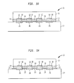
- (a) forming a first polymeric material on a surface of a semiconductor wafer having interconnect pads disposed thereon;
- (b) patterning said first polymeric material to provide openings that expose said interconnect pads;
- (c) forming conductive bump material in said openings;
- (d) forming a second polymeric material over said first polymeric material and said conductive bump material;
- (e) dicing said semiconductor wafer into individual chips; and
- (f) bonding at least one of said individual chips to an external substrate, wherein during said bonding said conductive bump material penetrates said second polymeric material and contacts a surface of said external substrate.
- (a) forming a first polymeric material on a surface of a semiconductor wafer having conductive bump material disposed on portions thereof;
- (b) removing a portion of said first polymeric material so as to expose top surfaces of said conductive bump material;
- (c) forming a second polymeric material on said first polymeric material and said exposed top surfaces of said conductive bump material;
- (d) dicing said semiconductor wafer into individual chips; and
- (e) bonding at least one of said individual chips to an external substrate, wherein during said bonding said conductive bump material penetrates said second polymeric material and contacts a surface of said external substrate.
- a semiconductor chip having a surface wherein conductive bump material is disposed on portions thereof;
- a bilayer comprising a first polymeric material and a second polymeric material abutting said conductive bump material; and
- an external substrate bonded to said semiconductor chip by said conductive bump material.
Claims (22)
Priority Applications (1)
| Application Number | Priority Date | Filing Date | Title |
|---|---|---|---|
| US09/782,494 US6924171B2 (en) | 2001-02-13 | 2001-02-13 | Bilayer wafer-level underfill |
Applications Claiming Priority (1)
| Application Number | Priority Date | Filing Date | Title |
|---|---|---|---|
| US09/782,494 US6924171B2 (en) | 2001-02-13 | 2001-02-13 | Bilayer wafer-level underfill |
Publications (2)
| Publication Number | Publication Date |
|---|---|
| US20020109228A1 US20020109228A1 (en) | 2002-08-15 |
| US6924171B2 true US6924171B2 (en) | 2005-08-02 |
Family
ID=25126221
Family Applications (1)
| Application Number | Title | Priority Date | Filing Date |
|---|---|---|---|
| US09/782,494 Expired - Lifetime US6924171B2 (en) | 2001-02-13 | 2001-02-13 | Bilayer wafer-level underfill |
Country Status (1)
| Country | Link |
|---|---|
| US (1) | US6924171B2 (en) |
Cited By (29)
| Publication number | Priority date | Publication date | Assignee | Title |
|---|---|---|---|---|
| US20040219716A1 (en) * | 2002-11-13 | 2004-11-04 | Tessera, Inc. | Microelectronic assemblies having low profile connections |
| US20060003569A1 (en) * | 2002-07-08 | 2006-01-05 | Farnworth Warren M | Semiconductor devices with permanent polymer stencil and method for manufacturing the same |
| US20060046346A1 (en) * | 2004-09-01 | 2006-03-02 | Benson Peter A | Methods for packaging microfeature devices and microfeature devices formed by such methods |
| US20060068521A1 (en) * | 2004-09-29 | 2006-03-30 | Song-Hua Shi | Method of fabricating microelectronic package using no-flow underfill technology and microelectronic package formed according to the method |
| US20060097377A1 (en) * | 2004-11-09 | 2006-05-11 | Han-Shin Youn | Flip chip bonding structure using non-conductive adhesive and related fabrication method |
| US20060105497A1 (en) * | 2004-11-15 | 2006-05-18 | Daewoong Suh | Forming a stress compensation layer and structures formed thereby |
| US20060186518A1 (en) * | 2005-02-23 | 2006-08-24 | Kevin Wu | Module card structure |
| US20060211171A1 (en) * | 2005-03-18 | 2006-09-21 | Tummala Rao O | Underfill on substrate process and ultra-fine pitch, low standoff chip-to-package interconnections produced thereby |
| US20060289966A1 (en) * | 2005-06-22 | 2006-12-28 | Dani Ashay A | Silicon wafer with non-soluble protective coating |
| US20060289607A1 (en) * | 2005-06-28 | 2006-12-28 | Buchwalter Stephen L | Composite solder transfer moldplate structure and method of making same |
| US20070066048A1 (en) * | 2004-09-01 | 2007-03-22 | Benson Peter A | Method for creating electrically conductive elements for semiconductor device structures using laser ablation processes and methods of fabricating semiconductor device assemblies |
| US20070063325A1 (en) * | 2005-09-22 | 2007-03-22 | Chun-Hung Lin | Chip package structure and bumping process |
| US20080039560A1 (en) * | 2006-08-11 | 2008-02-14 | General Electric Company | Syneretic composition, associated method and article |
| US20080039608A1 (en) * | 2006-08-11 | 2008-02-14 | General Electric Company | Oxetane composition, associated method and article |
| US20080039542A1 (en) * | 2006-08-11 | 2008-02-14 | General Electric Company | Composition and associated method |
| US20080121845A1 (en) * | 2006-08-11 | 2008-05-29 | General Electric Company | Oxetane composition, associated method and article |
| US20080315424A1 (en) * | 2001-03-30 | 2008-12-25 | Megica Corporation | Structure and manufactruing method of chip scale package |
| US20090102070A1 (en) * | 2007-10-22 | 2009-04-23 | International Business Machines Corporation | Alignment Marks on the Edge of Wafers and Methods for Same |
| US20090108472A1 (en) * | 2007-10-29 | 2009-04-30 | International Business Machines Corporation | Wafer-level underfill process using over-bump-applied resin |
| US20090169886A1 (en) * | 2007-12-31 | 2009-07-02 | International Business Machines Corporation | Negative coefficient thermal expansion engineered particles for composite fabrication |
| US20090251698A1 (en) * | 2008-04-02 | 2009-10-08 | Claudius Feger | Method and system for collecting alignment data from coated chips or wafers |
| EP2141738A2 (en) | 2008-07-01 | 2010-01-06 | International Business Machines Corporation | Chip-level underfill process and structures |
| US20100129961A1 (en) * | 2008-11-25 | 2010-05-27 | International Business Machines Corporation | Multi chip stacking with reliable joining |
| US20110229822A1 (en) * | 2008-11-25 | 2011-09-22 | Stapleton Russell A | Methods for protecting a die surface with photocurable materials |
| US20130256857A1 (en) * | 2012-03-27 | 2013-10-03 | Infineon Technologies Ag | Semiconductor Packages and Methods of Formation Thereof |
| CN104008983A (en) * | 2014-05-04 | 2014-08-27 | 清华大学 | Metal protruding point manufacturing method |
| US9093448B2 (en) | 2008-11-25 | 2015-07-28 | Lord Corporation | Methods for protecting a die surface with photocurable materials |
| US9461007B2 (en) | 2014-07-11 | 2016-10-04 | Samsung Electronics Co., Ltd. | Wafer-to-wafer bonding structure |
| CN110544639A (en) * | 2019-08-23 | 2019-12-06 | 深圳宏芯宇电子股份有限公司 | Integrated circuit crystal grain mounting method and semiconductor device |
Families Citing this family (22)
| Publication number | Priority date | Publication date | Assignee | Title |
|---|---|---|---|---|
| US6352881B1 (en) * | 1999-07-22 | 2002-03-05 | National Semiconductor Corporation | Method and apparatus for forming an underfill adhesive layer |
| US6710454B1 (en) * | 2000-02-16 | 2004-03-23 | Micron Technology, Inc. | Adhesive layer for an electronic apparatus having multiple semiconductor devices |
| JP2002299378A (en) * | 2001-03-30 | 2002-10-11 | Lintec Corp | Adhesive sheet with conductor, method for manufacturing semiconductor device and the semiconductor device |
| US6660560B2 (en) * | 2001-09-10 | 2003-12-09 | Delphi Technologies, Inc. | No-flow underfill material and underfill method for flip chip devices |
| US7423337B1 (en) | 2002-08-19 | 2008-09-09 | National Semiconductor Corporation | Integrated circuit device package having a support coating for improved reliability during temperature cycling |
| TWI244129B (en) * | 2002-10-25 | 2005-11-21 | Via Tech Inc | Bonding column process |
| US7301222B1 (en) | 2003-02-12 | 2007-11-27 | National Semiconductor Corporation | Apparatus for forming a pre-applied underfill adhesive layer for semiconductor wafer level chip-scale packages |
| US6946384B2 (en) * | 2003-06-06 | 2005-09-20 | Intel Corporation | Stacked device underfill and a method of fabrication |
| US7320928B2 (en) * | 2003-06-20 | 2008-01-22 | Intel Corporation | Method of forming a stacked device filler |
| US20050212105A1 (en) * | 2004-03-23 | 2005-09-29 | Walk Michael J | Integrated circuit die and substrate coupling |
| US7282375B1 (en) | 2004-04-14 | 2007-10-16 | National Semiconductor Corporation | Wafer level package design that facilitates trimming and testing |
| TWI230989B (en) * | 2004-05-05 | 2005-04-11 | Megic Corp | Chip bonding method |
| US7067350B1 (en) * | 2005-01-31 | 2006-06-27 | Taiwan Semiconductor Manufacturing Company, Ltd. | Method of manufacturing a semiconductor device using electrical contacts formed in an isolation layer |
| US7410090B2 (en) * | 2006-04-21 | 2008-08-12 | International Business Machines Corporation | Conductive bonding material fill techniques |
| US7573138B2 (en) * | 2006-11-30 | 2009-08-11 | Taiwan Semiconductor Manufacturing Co., Ltd. | Stress decoupling structures for flip-chip assembly |
| US9314864B2 (en) | 2007-07-09 | 2016-04-19 | International Business Machines Corporation | C4NP compliant solder fill head seals |
| JP5004351B2 (en) * | 2007-11-30 | 2012-08-22 | 信越化学工業株式会社 | Manufacturing method of semiconductor device |
| US7931187B2 (en) * | 2008-11-12 | 2011-04-26 | International Business Machines Corporation | Injection molded solder method for forming solder bumps on substrates |
| US20110115099A1 (en) * | 2009-05-14 | 2011-05-19 | Vertical Circuits, Inc. | Flip-chip underfill |
| KR101677739B1 (en) | 2010-09-29 | 2016-11-21 | 삼성전자주식회사 | package for semiconductor device and manufacturing method of the same |
| JP2012124244A (en) * | 2010-12-07 | 2012-06-28 | Sony Chemical & Information Device Corp | Mounting method of semiconductor element and mounting body |
| US10858495B2 (en) * | 2016-03-24 | 2020-12-08 | Siltectra Gmbh | Polymer hybrid material for use in a splitting method |
Citations (17)
| Publication number | Priority date | Publication date | Assignee | Title |
|---|---|---|---|---|
| US3943623A (en) * | 1974-08-23 | 1976-03-16 | Nitto Electric Industrial Co., Ltd. | Hollow cavity package electronic unit |
| US4681654A (en) * | 1986-05-21 | 1987-07-21 | International Business Machines Corporation | Flexible film semiconductor chip carrier |
| US5153986A (en) * | 1991-07-17 | 1992-10-13 | International Business Machines | Method for fabricating metal core layers for a multi-layer circuit board |
| US5319244A (en) * | 1991-12-13 | 1994-06-07 | International Business Machines Corporation | Triazine thin film adhesives |
| US5895229A (en) * | 1997-05-19 | 1999-04-20 | Motorola, Inc. | Microelectronic package including a polymer encapsulated die, and method for forming same |
| US5909634A (en) * | 1996-12-20 | 1999-06-01 | Texas Instruments | Method and apparatus for forming solder on a substrate |
| US5930598A (en) * | 1996-05-01 | 1999-07-27 | Motorola, Inc. | Microelectronic assembly including a decomposable encapsulant, and method for forming and reworking same |
| US5975408A (en) * | 1997-10-23 | 1999-11-02 | Lucent Technologies Inc. | Solder bonding of electrical components |
| US6228678B1 (en) * | 1998-04-27 | 2001-05-08 | Fry's Metals, Inc. | Flip chip with integrated mask and underfill |
| US6346296B1 (en) * | 1999-09-14 | 2002-02-12 | Alliedsignal Inc. | Highly stable packaging substrates |
| US6372544B1 (en) * | 2000-06-23 | 2002-04-16 | Advanced Micro Devices, Inc. | Method to reduce occurrences of fillet cracking in flip-chip underfill |
| US6410415B1 (en) * | 1999-03-23 | 2002-06-25 | Polymer Flip Chip Corporation | Flip chip mounting technique |
| US20020105092A1 (en) * | 2001-02-02 | 2002-08-08 | Coyle Anthony L. | Flip chip semiconductor device in a molded chip scale package (CSP) and method of assembly |
| US6506681B2 (en) * | 2000-12-06 | 2003-01-14 | Micron Technology, Inc. | Thin flip—chip method |
| US20030199160A1 (en) * | 1996-05-21 | 2003-10-23 | Farnworth Warren M | Use of palladium in IC manufacturing with conductive polymer bump |
| US6656750B1 (en) * | 1999-04-29 | 2003-12-02 | International Business Machines Corporation | Method for testing chips on flat solder bumps |
| US6774493B2 (en) * | 1997-07-21 | 2004-08-10 | M. A. Capote | Semiconductor flip-chip package and method for the fabrication thereof |
-
2001
- 2001-02-13 US US09/782,494 patent/US6924171B2/en not_active Expired - Lifetime
Patent Citations (17)
| Publication number | Priority date | Publication date | Assignee | Title |
|---|---|---|---|---|
| US3943623A (en) * | 1974-08-23 | 1976-03-16 | Nitto Electric Industrial Co., Ltd. | Hollow cavity package electronic unit |
| US4681654A (en) * | 1986-05-21 | 1987-07-21 | International Business Machines Corporation | Flexible film semiconductor chip carrier |
| US5153986A (en) * | 1991-07-17 | 1992-10-13 | International Business Machines | Method for fabricating metal core layers for a multi-layer circuit board |
| US5319244A (en) * | 1991-12-13 | 1994-06-07 | International Business Machines Corporation | Triazine thin film adhesives |
| US5930598A (en) * | 1996-05-01 | 1999-07-27 | Motorola, Inc. | Microelectronic assembly including a decomposable encapsulant, and method for forming and reworking same |
| US20030199160A1 (en) * | 1996-05-21 | 2003-10-23 | Farnworth Warren M | Use of palladium in IC manufacturing with conductive polymer bump |
| US5909634A (en) * | 1996-12-20 | 1999-06-01 | Texas Instruments | Method and apparatus for forming solder on a substrate |
| US5895229A (en) * | 1997-05-19 | 1999-04-20 | Motorola, Inc. | Microelectronic package including a polymer encapsulated die, and method for forming same |
| US6774493B2 (en) * | 1997-07-21 | 2004-08-10 | M. A. Capote | Semiconductor flip-chip package and method for the fabrication thereof |
| US5975408A (en) * | 1997-10-23 | 1999-11-02 | Lucent Technologies Inc. | Solder bonding of electrical components |
| US6228678B1 (en) * | 1998-04-27 | 2001-05-08 | Fry's Metals, Inc. | Flip chip with integrated mask and underfill |
| US6410415B1 (en) * | 1999-03-23 | 2002-06-25 | Polymer Flip Chip Corporation | Flip chip mounting technique |
| US6656750B1 (en) * | 1999-04-29 | 2003-12-02 | International Business Machines Corporation | Method for testing chips on flat solder bumps |
| US6346296B1 (en) * | 1999-09-14 | 2002-02-12 | Alliedsignal Inc. | Highly stable packaging substrates |
| US6372544B1 (en) * | 2000-06-23 | 2002-04-16 | Advanced Micro Devices, Inc. | Method to reduce occurrences of fillet cracking in flip-chip underfill |
| US6506681B2 (en) * | 2000-12-06 | 2003-01-14 | Micron Technology, Inc. | Thin flip—chip method |
| US20020105092A1 (en) * | 2001-02-02 | 2002-08-08 | Coyle Anthony L. | Flip chip semiconductor device in a molded chip scale package (CSP) and method of assembly |
Cited By (52)
| Publication number | Priority date | Publication date | Assignee | Title |
|---|---|---|---|---|
| US9018774B2 (en) | 2001-03-30 | 2015-04-28 | Qualcomm Incorporated | Chip package |
| US8912666B2 (en) | 2001-03-30 | 2014-12-16 | Qualcomm Incorporated | Structure and manufacturing method of chip scale package |
| US8748227B2 (en) * | 2001-03-30 | 2014-06-10 | Megit Acquisition Corp. | Method of fabricating chip package |
| US8426982B2 (en) | 2001-03-30 | 2013-04-23 | Megica Corporation | Structure and manufacturing method of chip scale package |
| US20080315424A1 (en) * | 2001-03-30 | 2008-12-25 | Megica Corporation | Structure and manufactruing method of chip scale package |
| US20060003569A1 (en) * | 2002-07-08 | 2006-01-05 | Farnworth Warren M | Semiconductor devices with permanent polymer stencil and method for manufacturing the same |
| US7589010B2 (en) * | 2002-07-08 | 2009-09-15 | Micron Technology, Inc. | Semiconductor devices with permanent polymer stencil and method for manufacturing the same |
| US20060275951A1 (en) * | 2002-11-13 | 2006-12-07 | Tessera, Inc. | Microelectronic assemblies having low profile connections |
| US7098074B2 (en) * | 2002-11-13 | 2006-08-29 | Tessera, Inc. | Microelectronic assemblies having low profile connections |
| US20040219716A1 (en) * | 2002-11-13 | 2004-11-04 | Tessera, Inc. | Microelectronic assemblies having low profile connections |
| US7579684B2 (en) | 2004-09-01 | 2009-08-25 | Micron Technology, Inc. | Methods for packing microfeature devices and microfeature devices formed by such methods |
| US20060205116A1 (en) * | 2004-09-01 | 2006-09-14 | Micron Technology, Inc. | Methods for packaging microfeature devices and microfeature devices formed by such methods |
| US7157310B2 (en) * | 2004-09-01 | 2007-01-02 | Micron Technology, Inc. | Methods for packaging microfeature devices and microfeature devices formed by such methods |
| US20070066048A1 (en) * | 2004-09-01 | 2007-03-22 | Benson Peter A | Method for creating electrically conductive elements for semiconductor device structures using laser ablation processes and methods of fabricating semiconductor device assemblies |
| US7629250B2 (en) | 2004-09-01 | 2009-12-08 | Micron Technology, Inc. | Method for creating electrically conductive elements for semiconductor device structures using laser ablation processes and methods of fabricating semiconductor device assemblies |
| US20060046346A1 (en) * | 2004-09-01 | 2006-03-02 | Benson Peter A | Methods for packaging microfeature devices and microfeature devices formed by such methods |
| US20060068521A1 (en) * | 2004-09-29 | 2006-03-30 | Song-Hua Shi | Method of fabricating microelectronic package using no-flow underfill technology and microelectronic package formed according to the method |
| US20060097377A1 (en) * | 2004-11-09 | 2006-05-11 | Han-Shin Youn | Flip chip bonding structure using non-conductive adhesive and related fabrication method |
| US20180182697A1 (en) * | 2004-11-15 | 2018-06-28 | Intel Corporation | Forming a stress compensation layer and structures formed thereby |
| US9929080B2 (en) * | 2004-11-15 | 2018-03-27 | Intel Corporation | Forming a stress compensation layer and structures formed thereby |
| US20060105497A1 (en) * | 2004-11-15 | 2006-05-18 | Daewoong Suh | Forming a stress compensation layer and structures formed thereby |
| US7233060B2 (en) * | 2005-02-23 | 2007-06-19 | Kingpak Technology Inc. | Module card structure |
| US20060186518A1 (en) * | 2005-02-23 | 2006-08-24 | Kevin Wu | Module card structure |
| US20060211171A1 (en) * | 2005-03-18 | 2006-09-21 | Tummala Rao O | Underfill on substrate process and ultra-fine pitch, low standoff chip-to-package interconnections produced thereby |
| US20060289966A1 (en) * | 2005-06-22 | 2006-12-28 | Dani Ashay A | Silicon wafer with non-soluble protective coating |
| US20060289607A1 (en) * | 2005-06-28 | 2006-12-28 | Buchwalter Stephen L | Composite solder transfer moldplate structure and method of making same |
| US20070063325A1 (en) * | 2005-09-22 | 2007-03-22 | Chun-Hung Lin | Chip package structure and bumping process |
| US20080039608A1 (en) * | 2006-08-11 | 2008-02-14 | General Electric Company | Oxetane composition, associated method and article |
| US20080039560A1 (en) * | 2006-08-11 | 2008-02-14 | General Electric Company | Syneretic composition, associated method and article |
| US20080039542A1 (en) * | 2006-08-11 | 2008-02-14 | General Electric Company | Composition and associated method |
| US20080121845A1 (en) * | 2006-08-11 | 2008-05-29 | General Electric Company | Oxetane composition, associated method and article |
| US20090102070A1 (en) * | 2007-10-22 | 2009-04-23 | International Business Machines Corporation | Alignment Marks on the Edge of Wafers and Methods for Same |
| US20090108472A1 (en) * | 2007-10-29 | 2009-04-30 | International Business Machines Corporation | Wafer-level underfill process using over-bump-applied resin |
| US8138448B2 (en) * | 2007-12-31 | 2012-03-20 | International Business Machines Corporation | Negative coefficient thermal expansion engineered particles for composite fabrication |
| US20090169886A1 (en) * | 2007-12-31 | 2009-07-02 | International Business Machines Corporation | Negative coefficient thermal expansion engineered particles for composite fabrication |
| US8624152B2 (en) | 2007-12-31 | 2014-01-07 | International Business Machines Corporation | Negative coefficient thermal expansion engineered particles for composite fabrication |
| US20090251698A1 (en) * | 2008-04-02 | 2009-10-08 | Claudius Feger | Method and system for collecting alignment data from coated chips or wafers |
| US7773220B2 (en) | 2008-04-02 | 2010-08-10 | International Business Machines Corporation | Method and system for collecting alignment data from coated chips or wafers |
| US7951648B2 (en) | 2008-07-01 | 2011-05-31 | International Business Machines Corporation | Chip-level underfill method of manufacture |
| US20100003786A1 (en) * | 2008-07-01 | 2010-01-07 | International Business Machines Corporation | Chip-level underfill process and structures thereof |
| EP2141738A2 (en) | 2008-07-01 | 2010-01-06 | International Business Machines Corporation | Chip-level underfill process and structures |
| US20100129961A1 (en) * | 2008-11-25 | 2010-05-27 | International Business Machines Corporation | Multi chip stacking with reliable joining |
| US8568961B2 (en) | 2008-11-25 | 2013-10-29 | Lord Corporation | Methods for protecting a die surface with photocurable materials |
| US9093448B2 (en) | 2008-11-25 | 2015-07-28 | Lord Corporation | Methods for protecting a die surface with photocurable materials |
| US20110229822A1 (en) * | 2008-11-25 | 2011-09-22 | Stapleton Russell A | Methods for protecting a die surface with photocurable materials |
| US8866274B2 (en) * | 2012-03-27 | 2014-10-21 | Infineon Technologies Ag | Semiconductor packages and methods of formation thereof |
| US20130256857A1 (en) * | 2012-03-27 | 2013-10-03 | Infineon Technologies Ag | Semiconductor Packages and Methods of Formation Thereof |
| CN104008983A (en) * | 2014-05-04 | 2014-08-27 | 清华大学 | Metal protruding point manufacturing method |
| CN104008983B (en) * | 2014-05-04 | 2016-10-12 | 清华大学 | A kind of metal salient point manufacture method |
| US9461007B2 (en) | 2014-07-11 | 2016-10-04 | Samsung Electronics Co., Ltd. | Wafer-to-wafer bonding structure |
| CN110544639A (en) * | 2019-08-23 | 2019-12-06 | 深圳宏芯宇电子股份有限公司 | Integrated circuit crystal grain mounting method and semiconductor device |
| CN110544639B (en) * | 2019-08-23 | 2021-04-30 | 深圳宏芯宇电子股份有限公司 | Integrated circuit crystal grain mounting method and semiconductor device |
Also Published As
| Publication number | Publication date |
|---|---|
| US20020109228A1 (en) | 2002-08-15 |
Similar Documents
| Publication | Publication Date | Title |
|---|---|---|
| US6924171B2 (en) | Bilayer wafer-level underfill | |
| US6294405B1 (en) | Method of forming semiconductor device having a sub-chip-scale package structure | |
| JP5007127B2 (en) | Integrated circuit device manufacturing method and manufacturing apparatus using self-organizing function | |
| US5909057A (en) | Integrated heat spreader/stiffener with apertures for semiconductor package | |
| US6166434A (en) | Die clip assembly for semiconductor package | |
| US7442578B2 (en) | Underfill compounds including electrically charged filler elements, microelectronic devices having underfill compounds including electrically charged filler elements, and methods of underfilling micoelectronic devices | |
| US6732913B2 (en) | Method for forming a wafer level chip scale package, and package formed thereby | |
| US20080318363A1 (en) | Stack circuit member and method | |
| US20090115042A1 (en) | Semiconductor device having three-dimensional stacked structure and method of fabricating the same | |
| US11508671B2 (en) | Semiconductor package and manufacturing method thereof | |
| JP3450236B2 (en) | Semiconductor device and manufacturing method thereof | |
| US6861285B2 (en) | Flip chip underfill process | |
| US20060121646A1 (en) | Wafer-level underfill process making use of sacrificial contact pad protective material | |
| US6773958B1 (en) | Integrated assembly-underfill flip chip process | |
| US20030214007A1 (en) | Wafer-level package with bump and method for manufacturing the same | |
| US6002171A (en) | Integrated heat spreader/stiffener assembly and method of assembly for semiconductor package | |
| US7141487B2 (en) | Method for ultra thinning bumped wafers for flip chip | |
| US7951648B2 (en) | Chip-level underfill method of manufacture | |
| JP3621182B2 (en) | Manufacturing method of chip size package | |
| US6916687B2 (en) | Bump process for flip chip package | |
| US20040082108A1 (en) | Method of making an electronic package | |
| US6690090B2 (en) | Semiconductor device having reliable coupling with mounting substrate | |
| US6978540B2 (en) | Method for pre-applied thermoplastic reinforcement of electronic components | |
| US20040238925A1 (en) | Pre-applied thermoplastic reinforcement for electronic components | |
| US20040232530A1 (en) | Pre-applied thermoplastic reinforcement for electronic components |
Legal Events
| Date | Code | Title | Description |
|---|---|---|---|
| AS | Assignment |
Owner name: INTERNATIONAL BUSINESS MACHINES CORPORATION, NEW Y Free format text: ASSIGNMENT OF ASSIGNORS INTEREST;ASSIGNORS:BUCHWALTER, STEPHEN L.;DANOVITCH, DAVID;DOANY, FUAD ELIAS;AND OTHERS;REEL/FRAME:012068/0230;SIGNING DATES FROM 20010612 TO 20010716 |
|
| FEPP | Fee payment procedure |
Free format text: PAYOR NUMBER ASSIGNED (ORIGINAL EVENT CODE: ASPN); ENTITY STATUS OF PATENT OWNER: LARGE ENTITY |
|
| STCF | Information on status: patent grant |
Free format text: PATENTED CASE |
|
| CC | Certificate of correction | ||
| FPAY | Fee payment |
Year of fee payment: 4 |
|
| REMI | Maintenance fee reminder mailed | ||
| FPAY | Fee payment |
Year of fee payment: 8 |
|
| SULP | Surcharge for late payment |
Year of fee payment: 7 |
|
| FPAY | Fee payment |
Year of fee payment: 12 |