US6919740B2 - Molecular-junction-nanowire-crossbar-based inverter, latch, and flip-flop circuits, and more complex circuits composed, in part, from molecular-junction-nanowire-crossbar-based inverter, latch, and flip-flop circuits - Google Patents
Molecular-junction-nanowire-crossbar-based inverter, latch, and flip-flop circuits, and more complex circuits composed, in part, from molecular-junction-nanowire-crossbar-based inverter, latch, and flip-flop circuits Download PDFInfo
- Publication number
- US6919740B2 US6919740B2 US10/355,850 US35585003A US6919740B2 US 6919740 B2 US6919740 B2 US 6919740B2 US 35585003 A US35585003 A US 35585003A US 6919740 B2 US6919740 B2 US 6919740B2
- Authority
- US
- United States
- Prior art keywords
- nanoscale
- nanowire
- signal line
- state
- junction
- Prior art date
- Legal status (The legal status is an assumption and is not a legal conclusion. Google has not performed a legal analysis and makes no representation as to the accuracy of the status listed.)
- Expired - Fee Related, expires
Links
Images
Classifications
-
- G—PHYSICS
- G11—INFORMATION STORAGE
- G11C—STATIC STORES
- G11C13/00—Digital stores characterised by the use of storage elements not covered by groups G11C11/00, G11C23/00, or G11C25/00
- G11C13/0002—Digital stores characterised by the use of storage elements not covered by groups G11C11/00, G11C23/00, or G11C25/00 using resistive RAM [RRAM] elements
- G11C13/0009—RRAM elements whose operation depends upon chemical change
- G11C13/0014—RRAM elements whose operation depends upon chemical change comprising cells based on organic memory material
-
- B—PERFORMING OPERATIONS; TRANSPORTING
- B82—NANOTECHNOLOGY
- B82Y—SPECIFIC USES OR APPLICATIONS OF NANOSTRUCTURES; MEASUREMENT OR ANALYSIS OF NANOSTRUCTURES; MANUFACTURE OR TREATMENT OF NANOSTRUCTURES
- B82Y10/00—Nanotechnology for information processing, storage or transmission, e.g. quantum computing or single electron logic
-
- G—PHYSICS
- G11—INFORMATION STORAGE
- G11C—STATIC STORES
- G11C13/00—Digital stores characterised by the use of storage elements not covered by groups G11C11/00, G11C23/00, or G11C25/00
- G11C13/02—Digital stores characterised by the use of storage elements not covered by groups G11C11/00, G11C23/00, or G11C25/00 using elements whose operation depends upon chemical change
-
- G—PHYSICS
- G11—INFORMATION STORAGE
- G11C—STATIC STORES
- G11C2213/00—Indexing scheme relating to G11C13/00 for features not covered by this group
- G11C2213/70—Resistive array aspects
- G11C2213/77—Array wherein the memory element being directly connected to the bit lines and word lines without any access device being used
-
- G—PHYSICS
- G11—INFORMATION STORAGE
- G11C—STATIC STORES
- G11C2213/00—Indexing scheme relating to G11C13/00 for features not covered by this group
- G11C2213/70—Resistive array aspects
- G11C2213/81—Array wherein the array conductors, e.g. word lines, bit lines, are made of nanowires
-
- H—ELECTRICITY
- H10—SEMICONDUCTOR DEVICES; ELECTRIC SOLID-STATE DEVICES NOT OTHERWISE PROVIDED FOR
- H10K—ORGANIC ELECTRIC SOLID-STATE DEVICES
- H10K10/00—Organic devices specially adapted for rectifying, amplifying, oscillating or switching; Organic capacitors or resistors having a potential-jump barrier or a surface barrier
- H10K10/701—Organic molecular electronic devices
-
- H—ELECTRICITY
- H10—SEMICONDUCTOR DEVICES; ELECTRIC SOLID-STATE DEVICES NOT OTHERWISE PROVIDED FOR
- H10K—ORGANIC ELECTRIC SOLID-STATE DEVICES
- H10K19/00—Integrated devices, or assemblies of multiple devices, comprising at least one organic element specially adapted for rectifying, amplifying, oscillating or switching, covered by group H10K10/00
-
- H—ELECTRICITY
- H10—SEMICONDUCTOR DEVICES; ELECTRIC SOLID-STATE DEVICES NOT OTHERWISE PROVIDED FOR
- H10K—ORGANIC ELECTRIC SOLID-STATE DEVICES
- H10K85/00—Organic materials used in the body or electrodes of devices covered by this subclass
- H10K85/20—Carbon compounds, e.g. carbon nanotubes or fullerenes
- H10K85/221—Carbon nanotubes
-
- H—ELECTRICITY
- H10—SEMICONDUCTOR DEVICES; ELECTRIC SOLID-STATE DEVICES NOT OTHERWISE PROVIDED FOR
- H10K—ORGANIC ELECTRIC SOLID-STATE DEVICES
- H10K85/00—Organic materials used in the body or electrodes of devices covered by this subclass
- H10K85/60—Organic compounds having low molecular weight
- H10K85/615—Polycyclic condensed aromatic hydrocarbons, e.g. anthracene
-
- Y—GENERAL TAGGING OF NEW TECHNOLOGICAL DEVELOPMENTS; GENERAL TAGGING OF CROSS-SECTIONAL TECHNOLOGIES SPANNING OVER SEVERAL SECTIONS OF THE IPC; TECHNICAL SUBJECTS COVERED BY FORMER USPC CROSS-REFERENCE ART COLLECTIONS [XRACs] AND DIGESTS
- Y10—TECHNICAL SUBJECTS COVERED BY FORMER USPC
- Y10S—TECHNICAL SUBJECTS COVERED BY FORMER USPC CROSS-REFERENCE ART COLLECTIONS [XRACs] AND DIGESTS
- Y10S977/00—Nanotechnology
- Y10S977/902—Specified use of nanostructure
- Y10S977/932—Specified use of nanostructure for electronic or optoelectronic application
- Y10S977/94—Specified use of nanostructure for electronic or optoelectronic application in a logic circuit
Definitions
- the present invention relates to electrical circuitry and, in particular, to programmanble, nanoscale-sized electrical circuits, including latches and flip-flops, configured from molecular-junction-nanowire crossbars that may be integrated with additional components in extremely dense electrical subsystems.
- nanoscale electronic devices generally employ nanoscale signal lines having widths, and nanoscale components having dimensions, of less than 100 nanometers. More densely fabricated nanoscale electronic devices may employ nanoscale signal lines having widths, and nanoscale components having dimensions, of less than 50 nanometers.
- the present invention provides techniques for implementing familiar electronic circuits at nanoscale sizes using molecular-junction-nanowire crossbars.
- a 3-state inverter is implemented.
- two 3-state inverter circuits are combined to produce a transparent latch.
- the 3-state inverter circuit and transparent-latch circuit can then be used as a basis for composing additional circuitry, including master/slave flip-flops, a transparent latch with asynchronous preset, a transparent latch with asynchronous clear, and a master/slave flip-flop with asynchronous preset.
- 3-state inverters can be used to compose latches and flip-flops, and latches and flip-flops can be used, along with additional Boolean circuitry, to compose a wide variety of useful, state-maintaining circuits.
- the 3-state inverters, latches, flip-flops, and other, more complex state-maintaining circuits can all be implemented within molecular-junction-nanowire crossbars by selectively configuring junctions within the molecular-junction-nanowire crossbars.
- Molecular-junction-nanowire crossbars are quite defect and fault tolerant, and can be configured using a variety of different topologies. Molecular-junction-nanowire crossbar implementations of circuits consume very little power, and have extremely high densities. These extremely dense circuits can then be combined into extremely dense subsystems that include many additional electrical components, implemented within a set of complementary/symmetry (“CS”) lattices.
- CS complementary/symmetry
- FIG. 1 illustrates a basic molecular-junction-nanowire crossbar.
- FIG. 2 illustrates a junction, or intersection, between two roughly orthogonal nanowires.
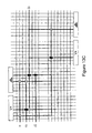
- FIG. 3 illustrates one possible approach for configuring a network of nanoscale electrical components from a two-dimensional molecular-junction-nanowire crossbar.
- FIG. 4 schematically illustrates a number of simple electrical components that can be programmed at the junctions of nanowires in molecular-junction-nanowire crossbars.
- FIG. 5 illustrates an exemplary CS lattice.
- FIGS. 6A-6B describe a 3-state inverter.
- FIG. 7 shows an implementation of a 3-state inverter in a CS lattice.
- FIGS. 8-9 illustrate operation of the 3-state inverter shown in FIG. 7 .
- FIGS. 10A-10B show a schematic representation of a transparent latch and a truth table for the transparent latch.
- FIG. 11 illustrates implementation of a transparent latch in a molecular-junction-nanowire crossbar.
- FIGS. 12A-12C illustrate operation of the transparent latch, shown in FIG. 11 , when the input enable input lines G and ⁇ overscore (G) ⁇ are in the states “1” and “0,” respectively.
- FIGS. 13A-C illustrate operation of the transparent latch, shown in FIG. 11 , when the enable input lines G and ⁇ overscore (G) ⁇ are in the states “0” and “1,” respectively.
- FIG. 14A shows a schematic for the combination of two transparent latches to form a master/slave flip-flop.
- FIG. 14B shows a modification of the transparent latch, as shown in FIG. 10A , with a NAND component replacing the simple inverter ( 1008 in FIG. 10A ) to produce a transparent latch with asynchronous preset.
- FIG. 14C shows a full CS-lattice implementation of the transparent latch with asynchronous preset.
- FIG. 14D shows a modification of the transparent latch, as shown in FIG. 10A , with a NOR element replacing the simple inverter ( 1008 in FIG. 10A ) to produce a transparent latch with asynchronous clear.
- FIG. 14E shows a full CS-lattice implementation of the transparent latch with asynchronous clear.
- FIGS. 15A and 15B show a combination of a transparent latch and a transparent latch with asynchronous clear to produce a master/slave flip-flop with asynchronous clear.
- molecular-junction-nanowire crossbars represent one of a number of emerging nanoscale electronic circuit configuration media that can be used to construct nanoscale electronic circuits.
- Various techniques have been developed to selectively configure different types of electronic components, such as transistors, resistors, diodes, and conductions, at the junctions between the conductive paths at two different layers of a molecular-junction-nanowire crossbar.
- the present invention provides methods for configuring more complex, familiar electronic circuits using selective configuration of simple electronic components within molecular-junction-nanowire crossbars.
- molecular-junction-nanowire crossbars are described.
- a number of embodiments of the present invention that employ molecular-junction-nanowire-crossbar technology are described.
- FIG. 1 illustrates a molecular-junction-nanowire crossbar.
- a first layer of approximately parallel nanowires 102 is overlain by a second layer of approximately parallel nanowires 104 roughly perpendicular, in orientation, to the nanowires of the first layer 102 , although the orientation angle between the layers may vary.
- the two layers of nanowires form a lattice, or crossbar, each nanowire of the second layer 104 overlying all of the nanowires of the first layer 102 and coming into close contact with each nanowire of the first layer 102 at intersection points, or junctions that represent the closest contact between two nanowires.
- Nanowires can be fabricated using mechanical nanoprinting techniques. Alternatively, nanowires can be chemically synthesized and can be deposited as layers of nanowires in one or a few process steps. Other alternative techniques for fabricating nanowires may also be employed. Thus, a two-dimensional molecular-junction-nanowire crossbar comprising first and second layers, as shown in FIG. 1 , can be manufactured via a relatively straightforward process. Many different types of conductive and semi-conductive nanowires can be chemically synthesized from metallic and semiconductor substances, from combinations of these types of substances, and from other types of substances. A molecular-junction-nanowire crossbar may be connected to microscale signal-line leads or other electronic leads through a variety of different methods to incorporate the nanowires into electrical circuits.
- FIG. 2 illustrates a junction between nanowires of two contiguous layers within a molecular-junction-nanowire crossbar.
- the junction between a first nanowire 202 of a first nanowire layer intersects a second nanowire 204 of a second nanowire layer. Note that the junction may or may not involve physical contact between the two nanowires 202 and 204 .
- FIG. 2 illustrates a junction between a first nanowire 202 of a first nanowire layer.
- the two nanowires are not in physical contact at their closest point of approach, but the gap between them is spanned by a small number of molecules 206 - 209 .
- Various different types of molecules may be introduced at junctions for a variety of different purposes. In many cases, the molecules of a junction may be accessed, for various purposes, through different voltage levels or current levels placed on the nanowires forming the junction.
- the molecules spanning the junction in FIG. 2 may have various different quantum states in which the molecules exhibit resistive, semiconductor-like, or conductive electrical properties.
- the current passing between the two nanowires intersecting at a junction may be a nonlinear function of the voltage across the junction as a result of quantum-mechanical tunneling of electrons through relatively low-energy, unoccupied quantum states of the molecules.
- the quantum states, and relative energies of quantum states, of the molecules may be controlled by applying differential currents or voltages to the nanowires forming the interaction.
- molecules may be conductive in a reduced state, but may act as insulators in an oxidized state, with redox reactions controlled by voltage levels determining which of the quantum states the molecules inhabit.
- a molecular junction is anisotropic, having a polarity or direction with respect to physical properties, including electrical properties.
- This anisotropy may arise from different chemical and/or physical properties of nanowires in the two layers of a molecular-junction-nanowire crossbar, may arise from asymmetries of junction molecules combined with junction molecules being uniformly-oriented with respect to the nanowire layers, and may arise both from differences in the properties of the nanowires as well as junction-molecule asymmetries.
- the fact the molecular junctions may have polarities allows for controlling junction properties by applying positive and negative voltages to molecular junctions, eliciting forward and reverse currents within the molecular junctions.
- the nanowires may include outer coatings, such as outer coatings 210 and 212 .
- the outer coatings may serve to insulate nanowires from one another, may constitute the molecules that serve to span junctions when the nanowires are placed in contact with one another, or may serve as modulation-dopant-layers, which can be selectively activated to dope semiconductor nanowires. Both p-type and n-type modulation dopant coatings have been developed.
- the molecules spanning junctions between crossing nanowires may be introduced as a separate layer formed between layers of nanowires. In some cases, the state changes of junction molecules may not be reversible.
- the junction molecules may initially be resistive, and may be made conductive through application of relatively high voltages.
- the junction molecules may be conductive, but the molecules may be irreversibly damaged, along with portions of the nanowires proximal to the junctions, through application of very high voltage levels, resulting in disrupting conductivity between the two nanowires and breaking electrical connection between them.
- the junction molecules may transition reversibly from one state to another and back, so that the nanoscale electrical components configured at nanowire junctions may be reconfigured, or programmed, by application of differential voltages to selected nanowire junctions.
- FIG. 3 illustrates one possible approach to configuring a network of reconfigurable nanoscale electrical components from a two-dimensional molecular-junction-nanowire crossbar.
- FIGS. 3A-E a small 3 ⁇ 3 molecular-junction-nanowire crossbar is shown, with circles at all nine junctions to indicate the state of the junction molecules.
- the junction molecules may have certain semiconductor, or conductive properties, while in a second state, labeled “2” in FIGS. 3A-E , junction molecules may have different properties.
- the states of the junctions of the molecular-junction-nanowire crossbar 300 are indeterminate.
- each junction may be uniquely accessed by applying a write voltage, or configuring voltage, to the nanowires that form the junction in order to configure, or program, the junction to have the state “1.” For example, in FIG.
- a first write voltage v w′ is applied to horizontal nanowire 304 and a second write voltage v w′′ is applied to vertical nanowire 306 to change the state of the junction from “2” to “1.”
- Individual junctions may be configured through steps similar to the steps shown in FIG. 3C to finally result in a fully configured nanoscale component network as shown in FIG. 3 D.
- the states of junctions 302 , 308 , and 310 that form a downward-slanted diagonal through the molecular-junction-nanowire crossbar have been configured by selective application of write voltages.
- the nanoscale electrical component network can be used as a portion of an integrated circuit.
- Input voltages v i ′, v i ′′, and v i ′′′ may be applied to the nanoscale electrical component lattice as inputs 312 and output voltages v i ′, v o ′′, and v o ′′ 314 may be accessed as the result of operation of the nanoscale electrical component network that represents a portion of an integrated circuit.
- the input and output voltages v i ′, v i ′′, and v i ′′′ and v o ′, v o ′′, and v o ′′′ have relatively low magnitudes compared with the write voltages v w and the reset voltages v reset .
- the reset voltage v reset may be again applied to the molecular-junction-nanowire crossbar, as in FIG. 3B , and the device reconfigured, or reprogrammed, as shown in steps in FIGS. 3C-3D .
- the types of nanowires types of dopants employed in the case of semiconductor nanowires, and the types of junction molecules employed in the molecular-junction-nanowire crossbar, many different, but similar configuring processes may be used to configure molecular-junction-nanowire crossbars into nanowire-based electrical components networks.
- FIG. 3 is meant to illustrate a general process by which molecular-junction-nanowire crossbars may be configured as useful portions of electronic circuits.
- junctions of nanowires in molecular-junction-nanowire crossbars may be configured, in various techniques depending on the chemical nature of the nanowires and junction-spanning molecules, to form a wide variety of different, simple electronic devices.
- FIG. 4 schematically illustrates a number of simple electrical components that can be configured at the junctions of nanowires in molecular-junction-nanowire crossbars.
- a junction may represent (1) a simple conductive connection between the two nanowires, as shown in FIG. 4A ; (2) a diode that conducts current in only one direction between the two nanowires, as shown in FIG. 4B ; (3) a resistor, with the magnitude of resistance configurable by application of different configuring voltages, as shown in FIG.
- nFET negatively doped field-effect transistor
- pFET positively doped field-effect transistor
- FIG. 4E the crossing of two conductive nanowires, with the voltage and current associated with each nanowire completely independent from one another, as shown in FIG. 4 F.
- nFET negatively doped field-effect transistor
- pFET positively doped field-effect transistor
- FIG. 4F the crossing of two conductive nanowires, with the voltage and current associated with each nanowire completely independent from one another, as shown in FIG. 4 F.
- nFET shown in FIG. 4D
- a relatively low voltage state on the gate wire 402 results in current passing through the source/drain wire 404
- a relatively high voltage on the gate wire 402 prevents conduction of current on the source/drain nanowire 404 .
- a junction may also be configured as an insulator, essentially interrupting conduction at the junction with respect to both nanowires.
- a two-dimensional molecular-junction-nanowire crossbar may be constructed and then configured as a network of electrical components. Note also that a junction, although shown in FIGS.
- 4A-F to comprise the junction of two single nanowires may also comprise a number of junctions between a number of wires in a first layer of a molecular-junction-nanowire crossbar that together comprise a single conductive element and the nanowires in a second nanowire layer that together comprise a second conductive element.
- the configurable electrical resistance of molecular junctions is an important and special property of molecular junctions.
- the initially relatively high resistance of the molecular junction may be lowered by applying a relatively large positive voltage to the molecular junction.
- the resistance of the molecular junction is generally a function of the magnitude of the highest voltage applied to the junction.
- the resistance of the junction can be made lower and lower.
- a relatively low resistance state achieved by application of a positive voltage may be reversed by applying a sufficiently high, negative voltage.
- the electrical resistance may also be reconfigurable, depending on the type of molecules forming the molecular junction.
- FIG. 5 illustrates an exemplary CS lattice. Note that, although CS lattices are generally configured to represent logical and useful circuits, the CS lattice in FIG. 5 is rather arbitrarily configured, and is shown not as a representation of a particular subcircuit implemented by the CS lattice, and may not even be useful or functional, but rather is included to show the basic features of the CS lattice itself.
- microregion 501 is chemically altered so that junctions within microregion 501 may be selectively configured as nFET components.
- microregion 502 has been chemically altered so that junctions within subregion 502 may be selectively configured as pFET components.
- the microregions 503 and 504 have been chemically configured so that junctions within microregions 503 and 504 can be selectively configured as conductive links that electrically connect the nanowires forming the junctions.
- the vertical semiconductive nanowires in FIG. 5 may be of nanoscale dimensions or of greater, sub-mircoscale or microscale dimensions, while the other set of parallel wires, the vertical semiconductive nanowires in FIG. 5 , need to be of nanoscale dimensions in order for a CS-lattice-based circuit to properly function.
- some number of nanowires is considered as a set of molecular input-signal lines.
- horizontal nanowires 506 - 513 are considered as inputs, and labeled “in 1 ”-“in 8 .”
- a distinct set of wires is normally considered as a set of molecular output-signal lines.
- horizontal nanowires 514 - 518 are considered as molecular output-signal lines, and designated in FIG.
- molecular output-signal line or horizontal nanowire, “out 5 ” 518 .
- molecular output-signal line “outs” is connected via junction connections 520 and 522 , denoted by small circles in the junctions, to vertical nanowires 524 and 526 , respectively.
- vertical wire 524 is connected with molecular input-signal line “in 3 ” 508 via an nFET 528 and connected with molecular input-signal line “in 5 ” 513 via an nFET 529 .
- molecular input-signal lines “in 3 ” 508 and “in 5 ” 513 are low, the nFETs 528 and 529 are activated to connect molecular output-signal line “out 5 ” with a high voltage source 530 , potentially driving molecular output-signal line “out 5 ” to a high-voltage state.
- molecular input-signal lines “in 1 ” and “in 8 ” are both in a high-voltage, or ON, state, then the pFETs 532 and 534 are activated to interconnect the vertical nanowire 526 with ground 536 , essentially shorting vertical nanowire 526 and molecular output-signal line “out 5 ” 518 to ground.
- molecular input-signal lines “in 1 ” and “in 8 ” are high, or ON, molecular output-signal line “out 5 ” 518 is low, or OFF.
- molecular output-signal line “out 5 ” is undriven, and in a high impedance state.
- the state of molecular output-signal line “out 5 ” 518 depends only on the states of molecular input-signal lines “in 1 ,” “in 3 ,” and “in 8 ,” and a truth table summarizing the response of molecular output-signal line to all possible input-signal-line-states can be provided as follows:
- CS lattices Various different types and sizes are possible.
- the configuration of CS lattices is constrained only by the fact that there is a minimum area of a molecular-junction-nanowire crossbar to which discrete types of chemically modifying agents can be applied, by direct deposit, by photolithographic methods, or by other methods.
- CS lattices comprise blocks of sublattices, or microregions, within which one or a small number of different types of nanoscale electrical components can be selectively created at nanowire junctions.
- FIGS. 6A-B describe a 3-state inverter.
- FIG. 6A shows a schematic rendering of a 3-state inverter
- FIG. 6B is a truth table showing the output signal from a 3-state inverter produced by different possible input values.
- a 3-state inverter 602 receives an input signal 604 as well as an enable signal line 605 and its complement ⁇ overscore (enable) ⁇ 606 . Based on the values of the input signal “in” and the complementary values of the enable and ⁇ overscore (enable) ⁇ input signal lines, a “0,” “1,” or undriven, high-Z state is produced on the output signal line 608 .
- the 3-state inverter inverts the input signal line “in” to the output signal line ⁇ overscore (out) ⁇ .
- the 3-state inverter outputs “0.”
- the output signal line is undriven, and in a high impedence state, shown in FIG. 6B as “high Z.”
- FIG. 7 shows an implementation of a 3-state inverter in a complementary/symmetry lattice (“CS lattice”).
- the top, left-hand microregion 702 is prepared for selective configuration of nFETs
- the top right-hand microregion 704 is prepared for selective configuration of pFETs
- the bottom two microregions 706 and 707 are prepared for selective configuration of connections.
- Three horizontal nanoscale signal lines, or nanowires, 708 , 710 , and 712 are chosen for the input signal lines “in,” “enable,” and “enable-complement,” respectively.
- a fourth horizontal nanowire 714 is chosen for the output signal line ⁇ overscore (out) ⁇ .
- Two vertical nanowires 716 and 718 are chosen for potentially interconnecting the output signal line ⁇ overscore (out) ⁇ 714 with a high voltage source 720 and with ground 722 .
- the input signal line “in” is potentially connected to these two vertical nanowires 716 and 718 via an nFET 724 and a pFET 726 .
- the input signal line enable is potentially interconnected with the second vertical nanowire 718 by a selectively configured pFET 728 , and its complement input signal line ⁇ overscore (enable) ⁇ is potentially connected to the first vertical nanowire 716 via a selectively configured nFET 730 .
- FIGS. 8-9 illustrate operation of the 3-state inverter shown in FIG. 7 .
- the state of the enable and ⁇ overscore (enable) ⁇ signal lines 710 and 712 is “1” and “0,” respectively, pFET 728 is activated, connecting nanowire 710 with nanowire 718 , and nFET 730 is also activated, connecting nanowire 712 with nanowire 716 .
- the state of the output signal line ⁇ overscore (out) ⁇ 714 is determined by the state of the input signal line 708 .
- nFET 724 is activated and pFET 726 is not activated, resulting in interconnection of nanowires 714 and 716 with the positive voltage source 720 .
- the 3-state inverter is particularly useful as a building block for more complex, clock and latch circuitry.
- 2-state inverters When 2-state inverters are employed for such devices, the behavior of latches and flip-flops built from the 2-state inverters may depend on difficult-to-measure, hard-to-control-in-manufacturing characteristics, and may, as a result, appear to behave non-deterministically. In such devices, a variety or race conditions may be inherent, leading to difficult design, configuration, and testing problems.
- the 3-state inverter provides the high-impedance third state, clock and latch circuits built from 3-state inverters are far less dependent on small changes in physical characteristics, and do not contain the race conditions inherent in similar devices built from 2-state inverters. In essence, clock and latch circuits built from 3-state inverters appear to behave deterministically.
- 3-state inverter functionality implemented in molecular-junction-nanowire crossbars are even more particularly useful for building clock and latch circuits, and more complex circuits based on combinations of clock, latch, and Boolean circuits. Because of the ease of configuring junctions within molecular-junction-nanowire crossbars, complex circuits based on combinations of clock, latch, and Boolean circuits can be implemented within a single molecular-junction-nanowire crossbar, for example, a CS lattice having various tilings of different types of microregions. Unlike prior techniques, where the complex circuits are configured by combining simpler-circuit components, molecular-junction-nanowire-crossbar implementations allow for composition of such circuits within a single device via junction configuration.
- FIGS. 10A-B show a schematic representation of a transparent latch and a truth table for the transparent latch, respectively.
- a transparent latch 1002 comprises a first 3-state inverter 1004 , a second 3-state inverter 1006 , and a simple inverter 1008 .
- the truth table shown in FIG. 10B when the input enable lines G and ⁇ overscore (G) ⁇ have states “1” and “0,” respectively, then the state of the input signal line D is passed through to the output signal line Q.
- FIG. 11 illustrates implementation of a transparent latch in a molecular-junction-nanowire crossbar.
- the input is inverted from that shown in FIG. 10 B.
- the implemented transparent latch outputs ⁇ overscore (Q) ⁇ .
- Two side-by-side CS lattices are interconnected, with inversion and mirroring of one of the CS lattices, as shown in FIG. 11 .
- Three horizontal nanowires 1102 , 1104 , and 1106 are chosen for input signal lines D, G, and ⁇ overscore (G) ⁇ , respectively.
- a fourth horizontal nanowire 1108 is chosen for the output signal line ⁇ overscore (Q) ⁇ .
- microregions 1120 and 1122 are prepared for selective configuration of nFETs
- microregions 1124 and 1126 are prepared for selective configuration of pFETs
- the remaining microregions 1128 - 1131 are prepared for selective configuration of connections.
- FIGS. 12A-C illustrate operation of the transparent latch, shown in FIG. 11 , when the input enable input lines G and ⁇ overscore (G) ⁇ are in the states “1” and “0,” respectively.
- FIG. 12A when the enable signal lines G and ⁇ overscore (G) ⁇ are in the states “1” and “0,” respectively, nFET 1202 is active and pFET 1204 is active, potentially interconnecting horizontal nanowire 1116 with a relatively high-voltage source 1206 and ground 1208 via vertical nanowires 1110 and 1112 .
- the state of the horizontal nanowire 1116 is determined by the state of input signal line D 1102 .
- FIG. 12A illustrates operation of the transparent latch, shown in FIG. 11 , when the input enable input lines G and ⁇ overscore (G) ⁇ are in the states “1” and “0,” respectively.
- nFET 1202 is active
- pFET 1204 is active, potentially interconnecting horizontal nanowire 1116 with a relatively high-voltage
- nFET 1210 when the state of input signal line D 1102 is “1,” pFET 1210 is activated, shorting horizontal nanowire 1116 to ground, in turn activating nFET 1212 , which connects the output signal line ⁇ overscore (Q) ⁇ 1108 to a relatively high-voltage source 1214 .
- nFET 1216 when the state of the input sign line D 1102 is “0,” then nFET 1216 is activated, placing horizontal nanowire 1116 in the state “1,” which in turn activates nFET 1218 , shorting output signal line Q 1108 to ground.
- the output of the transparent latch implemented in the molecular-junction-nanowire crossbar represents inversion of the state of the input line D.
- FIGS. 13A-C illustrate operation of the transparent latch, shown in FIG. 11 , when the enable input lines G and ⁇ overscore (G) ⁇ are in the states “0” and “1,” respectively.
- nFET 1220 and pFET 1222 are activated, potentially interconnecting the output signal line 1108 with the horizontal nanowire 1116 .
- FIG. 14A shows a schematic for the combination of the two transparent latches to form a master/slave flip-flop.
- FIG. 14B shows a modification of the transparent latch, as shown in FIG. 10A , with a NAND component replacing the simple inverter ( 1008 in FIG. 10A ) to produce a transparent latch with asynchronous preset.
- FIG. 14C shows a full CS-lattice implementation of the transparent latch with asynchronous preset.
- FIG. 14D shows a modification of the transparent latch, as shown in FIG. 10A , with a NOR element replacing the simple inverter ( 1008 in FIG. 10A ) to produce a transparent latch with asynchronous clear.
- FIG. 14A shows a schematic for the combination of the two transparent latches to form a master/slave flip-flop.
- FIG. 14B shows a modification of the transparent latch, as shown in FIG. 10A , with a NAND component replacing the simple inverter ( 1008 in FIG. 10A ) to
- FIGS. 14E shows a full CS-lattice implementation of the transparent latch with asynchronous clear.
- FIGS. 15A and 15B show a combination of a transparent latch and a transparent latch with asynchronous clear to produce a master/slave flip-flop with asynchronous clear.
- FIG. 15B shows combination of a transparent latch with a transparent latch with asynchronous reset to produce a master/slave flip-flop with asynchronous preset.
- Molecular-junction-nanowire crossbars are quite defect and fault tolerant, and can be configured using a variety of different topologies. Molecular-junction-nanowire crossbar implementations of circuits consume very little power, and have extremely high densities. These extremely dense circuits can then be combined into extremely dense subsystems that include many additional electrical components, implemented within a set of CS lattices. Thus, rather than simply representing a miniaturization of existing electronic circuits, in isolation, the present invention provides for building electronic circuits into complex subsystems having transistor densities equal to, or greater than, 1 billion transistors/cm 2 or, in other words, having 1.0 giga-transistor/cm 2 densities and greater transistor densities.
Abstract
Description
in1 | in3 | in8 | |
||
0 | 0 | 0 | 1 | ||
0 | 0 | 1 | 1 | ||
0 | 1 | 0 | |
||
0 | 1 | 1 | |
||
1 | 0 | 0 | 1 | ||
1 | 0 | 1 | 0 | ||
1 | 1 | 0 | |
||
1 | 1 | 1 | 0 | ||
Claims (30)
Priority Applications (1)
Application Number | Priority Date | Filing Date | Title |
---|---|---|---|
US10/355,850 US6919740B2 (en) | 2003-01-31 | 2003-01-31 | Molecular-junction-nanowire-crossbar-based inverter, latch, and flip-flop circuits, and more complex circuits composed, in part, from molecular-junction-nanowire-crossbar-based inverter, latch, and flip-flop circuits |
Applications Claiming Priority (1)
Application Number | Priority Date | Filing Date | Title |
---|---|---|---|
US10/355,850 US6919740B2 (en) | 2003-01-31 | 2003-01-31 | Molecular-junction-nanowire-crossbar-based inverter, latch, and flip-flop circuits, and more complex circuits composed, in part, from molecular-junction-nanowire-crossbar-based inverter, latch, and flip-flop circuits |
Publications (2)
Publication Number | Publication Date |
---|---|
US20040149978A1 US20040149978A1 (en) | 2004-08-05 |
US6919740B2 true US6919740B2 (en) | 2005-07-19 |
Family
ID=32770639
Family Applications (1)
Application Number | Title | Priority Date | Filing Date |
---|---|---|---|
US10/355,850 Expired - Fee Related US6919740B2 (en) | 2003-01-31 | 2003-01-31 | Molecular-junction-nanowire-crossbar-based inverter, latch, and flip-flop circuits, and more complex circuits composed, in part, from molecular-junction-nanowire-crossbar-based inverter, latch, and flip-flop circuits |
Country Status (1)
Country | Link |
---|---|
US (1) | US6919740B2 (en) |
Cited By (109)
Publication number | Priority date | Publication date | Assignee | Title |
---|---|---|---|---|
US20050035787A1 (en) * | 2003-08-13 | 2005-02-17 | Nantero, Inc. | Nanotube-based switching elements and logic circuits |
US20050058797A1 (en) * | 2003-09-08 | 2005-03-17 | Nantero, Inc. | High purity nanotube fabrics and films |
US20050056825A1 (en) * | 2003-06-09 | 2005-03-17 | Nantero, Inc. | Field effect devices having a drain controlled via a nanotube switching element |
US20050065741A1 (en) * | 2003-05-14 | 2005-03-24 | Nantero, Inc. | Sensor platform using a non-horizontally oriented nanotube element |
US20050101112A1 (en) * | 2001-07-25 | 2005-05-12 | Nantero, Inc. | Methods of nanotubes films and articles |
US20050174842A1 (en) * | 2004-02-11 | 2005-08-11 | Nantero, Inc. | EEPROMS using carbon nanotubes for cell storage |
US20050237781A1 (en) * | 2003-06-09 | 2005-10-27 | Nantero, Inc. | Non-volatile electromechanical field effect devices and circuits using same and methods of forming same |
US20050281084A1 (en) * | 2001-12-28 | 2005-12-22 | Nantero, Inc. | Methods of making electromechanical three-trace junction devices |
US20060061389A1 (en) * | 2004-06-18 | 2006-03-23 | Nantero, Inc. | Integrated nanotube and field effect switching device |
US20060172521A1 (en) * | 2005-01-31 | 2006-08-03 | Snider Gregory S | Method for allocating resources in heterogeneous nanowire crossbars having defective nanowisre junctions |
US20060183278A1 (en) * | 2005-01-14 | 2006-08-17 | Nantero, Inc. | Field effect device having a channel of nanofabric and methods of making same |
US20060193093A1 (en) * | 2004-11-02 | 2006-08-31 | Nantero, Inc. | Nanotube ESD protective devices and corresponding nonvolatile and volatile nanotube switches |
US20060204427A1 (en) * | 2004-12-16 | 2006-09-14 | Nantero, Inc. | Aqueous carbon nanotube applicator liquids and methods for producing applicator liquids thereof |
US20060231865A1 (en) * | 2001-12-28 | 2006-10-19 | Nantero, Inc. | Electromechanical three-trace junction devices |
US20060237857A1 (en) * | 2005-01-14 | 2006-10-26 | Nantero, Inc. | Hybrid carbon nanotube FET(CNFET)-FET static RAM (SRAM) and method of making same |
US20060250843A1 (en) * | 2005-05-09 | 2006-11-09 | Nantero, Inc. | Non-volatile-shadow latch using a nanotube switch |
US20060260785A1 (en) * | 2005-05-13 | 2006-11-23 | Delta Electronics, Inc. | Heat sink |
US20060281287A1 (en) * | 2005-06-09 | 2006-12-14 | Yates Colin D | Method of aligning deposited nanotubes onto an etched feature using a spacer |
US20060281256A1 (en) * | 2005-06-08 | 2006-12-14 | Carter Richard J | Self-aligned cell integration scheme |
US20060292716A1 (en) * | 2005-06-27 | 2006-12-28 | Lsi Logic Corporation | Use selective growth metallization to improve electrical connection between carbon nanotubes and electrodes |
US20070004191A1 (en) * | 2005-06-30 | 2007-01-04 | Lsi Logic Corporation | Novel techniques for precision pattern transfer of carbon nanotubes from photo mask to wafers |
US20070015303A1 (en) * | 2003-08-13 | 2007-01-18 | Bertin Claude L | Nanotube device structure and methods of fabrication |
US20070094756A1 (en) * | 2005-10-21 | 2007-04-26 | Snider Gregory S | Nanoscale shift register and signal demultiplexing using microscale/nanoscale shift registers |
US20070210845A1 (en) * | 2004-06-18 | 2007-09-13 | Nantero, Inc. | Storage elements using nanotube switching elements |
US20070229112A1 (en) * | 2006-04-03 | 2007-10-04 | Blaise Laurent Mouttet | Programmable crossbar signal processor with op-amp outputs |
US20070233761A1 (en) * | 2006-04-03 | 2007-10-04 | Mouttet Blaise L | Crossbar arithmetic processor |
US7289357B2 (en) | 2003-08-13 | 2007-10-30 | Nantero, Inc. | Isolation structure for deflectable nanotube elements |
US7294877B2 (en) | 2003-03-28 | 2007-11-13 | Nantero, Inc. | Nanotube-on-gate FET structures and applications |
US7339401B2 (en) | 2003-08-13 | 2008-03-04 | Nantero, Inc. | Nanotube-based switching elements with multiple controls |
US20080079027A1 (en) * | 2004-06-09 | 2008-04-03 | Nantero, Inc. | Field effect devices having a gate controlled via a nanotube switching element |
US20080142850A1 (en) * | 2005-05-09 | 2008-06-19 | Nantero, Inc. | Memory elements and cross point switches and arrays of same using nonvolatile nanotube blocks |
US20080147954A1 (en) * | 2006-04-03 | 2008-06-19 | Blaise Laurent Mouttet | Crossbar arithmetic and summation processor |
US20080157127A1 (en) * | 2005-05-09 | 2008-07-03 | Nantero, Inc. | Nonvolatile nanotube diodes and nonvolatile nanotube blocks and systems using same and methods of making same |
US20080157257A1 (en) * | 2005-05-09 | 2008-07-03 | Nantero, Inc. | Nonvolatile nanotube diodes and nonvolatile nanotube blocks and systems using same and methods of making same |
US20080157126A1 (en) * | 2005-05-09 | 2008-07-03 | Nantero, Inc. | Nonvolatile nanotube diodes and nonvolatile nanotube blocks and systems using same and methods of making same |
US20080159042A1 (en) * | 2005-05-09 | 2008-07-03 | Bertin Claude L | Latch circuits and operation circuits having scalable nonvolatile nanotube switches as electronic fuse replacement elements |
US20080170429A1 (en) * | 2005-05-09 | 2008-07-17 | Nantero, Inc. | Nonvolatile nanotube diodes and nonvolatile nanotube blocks and systems using same and methods of making same |
US20080191742A1 (en) * | 2004-06-18 | 2008-08-14 | Bertin Claude L | Receiver circuit using nanotube-based switches and transistors |
US20080192532A1 (en) * | 2001-07-25 | 2008-08-14 | Segal Brent M | Hybrid circuit having nanotube memory cells |
US20080197881A1 (en) * | 2004-06-18 | 2008-08-21 | Bertin Claude L | Receiver circuit using nanotube-based switches and logic |
US20080212382A1 (en) * | 2006-04-03 | 2008-09-04 | Blaise Laurent Mouttet | Crossbar waveform driver circuit |
US20080212361A1 (en) * | 2005-05-09 | 2008-09-04 | Nantero, Inc. | Nonvolatile nanotube diodes and nonvolatile nanotube blocks and systems using same and methods of making same |
US20080231413A1 (en) * | 2004-09-21 | 2008-09-25 | Nantero, Inc. | Resistive elements using carbon nanotubes |
US20080231320A1 (en) * | 2004-06-18 | 2008-09-25 | Nantero, Inc. | Tri-state circuit using nanotube switching elements |
US20080238882A1 (en) * | 2007-02-21 | 2008-10-02 | Ramesh Sivarajan | Symmetric touch screen system with carbon nanotube-based transparent conductive electrode pairs |
US20080246116A1 (en) * | 2006-04-03 | 2008-10-09 | Blaise Laurent Mouttet | Symmetrical programmable crossbar structure |
US20080280038A1 (en) * | 2003-01-13 | 2008-11-13 | Nantero, Inc. | Methods of using thin metal layers to make carbon nanotube films, layers, fabrics, ribbons, elements and articles |
US20080290423A1 (en) * | 2003-08-13 | 2008-11-27 | Nantero, Inc. | Nanotube-based switching element |
US7479654B2 (en) | 2005-05-09 | 2009-01-20 | Nantero, Inc. | Memory arrays using nanotube articles with reprogrammable resistance |
US20090045473A1 (en) * | 2001-07-25 | 2009-02-19 | Nantero, Inc. | Devices having horizontally-disposed nanofabric articles and methods of making the same |
US20090052246A1 (en) * | 2005-05-09 | 2009-02-26 | Nantero, Inc. | Non-volatile shadow latch using a nanotube switch |
US20090051032A1 (en) * | 2003-09-08 | 2009-02-26 | Segal Brent M | Patterned nanoscopic articles and methods of making the same |
US20090099016A1 (en) * | 2005-12-19 | 2009-04-16 | Advanced Technology Materials, Inc. | Production of carbon nanotubes |
US20090115305A1 (en) * | 2007-05-22 | 2009-05-07 | Nantero, Inc. | Triodes using nanofabric articles and methods of making the same |
US20090140167A1 (en) * | 2005-09-06 | 2009-06-04 | Natero, Inc. | Nanotube fabric-based sensor systems and methods of making same |
US20090173964A1 (en) * | 2001-07-25 | 2009-07-09 | Nantero, Inc. | Method of forming a carbon nanotube-based contact to semiconductor |
US20090184389A1 (en) * | 2005-05-09 | 2009-07-23 | Bertin Claude L | Nonvolatile Nanotube Diodes and Nonvolatile Nanotube Blocks and Systems Using Same and Methods of Making Same |
US20090194839A1 (en) * | 2005-11-15 | 2009-08-06 | Bertin Claude L | Nonvolatile nanotube diodes and nonvolatile nanotube blocks and systems using same and methods of making same |
US20090211460A1 (en) * | 2007-11-20 | 2009-08-27 | Kwok Kuen So | Bowl and basket assembly and salad spinner incorporating such an assembly |
US7583526B2 (en) | 2003-08-13 | 2009-09-01 | Nantero, Inc. | Random access memory including nanotube switching elements |
US7598127B2 (en) | 2005-05-12 | 2009-10-06 | Nantero, Inc. | Nanotube fuse structure |
US20100001267A1 (en) * | 2008-06-20 | 2010-01-07 | Nantero, Inc. | Nram arrays with nanotube blocks, nanotube traces, and nanotube planes and methods of making same |
US7652342B2 (en) | 2004-06-18 | 2010-01-26 | Nantero, Inc. | Nanotube-based transfer devices and related circuits |
US20100039138A1 (en) * | 2008-08-14 | 2010-02-18 | Nantero, Inc. | Nonvolatile nanotube programmable logic devices and a nonvolatile nanotube field programmable gate array using same |
US20100072957A1 (en) * | 2004-06-18 | 2010-03-25 | Bertin Claude L | Nanotube-based logic driver circuits |
US7719067B2 (en) | 2001-07-25 | 2010-05-18 | Nantero, Inc. | Devices having vertically-disposed nanofabric articles and methods of making the same |
US20100147657A1 (en) * | 2004-11-02 | 2010-06-17 | Nantero, Inc. | Nanotube esd protective devices and corresponding nonvolatile and volatile nanotube switches |
US7745810B2 (en) | 2001-07-25 | 2010-06-29 | Nantero, Inc. | Nanotube films and articles |
US7781862B2 (en) | 2005-05-09 | 2010-08-24 | Nantero, Inc. | Two-terminal nanotube devices and systems and methods of making same |
US20100267205A1 (en) * | 2005-09-06 | 2010-10-21 | Lockheed Martin Corporation | Carbon nanotubes for the selective transfer of heat from electronics |
US7824946B1 (en) | 2005-03-11 | 2010-11-02 | Nantero, Inc. | Isolated metal plug process for use in fabricating carbon nanotube memory cells |
US20100283528A1 (en) * | 2003-03-28 | 2010-11-11 | Nantero, Inc. | Nanotube-on-gate fet structures and applications |
US20100327247A1 (en) * | 2005-09-06 | 2010-12-30 | Nantero, Inc. | Method and system of using nanotube fabrics as joule heating elements for memories and other applications |
US20110027497A1 (en) * | 2009-07-31 | 2011-02-03 | Nantero, Inc. | Anisotropic nanotube fabric layers and films and methods of forming same |
US20110034008A1 (en) * | 2009-08-07 | 2011-02-10 | Nantero, Inc. | Method for forming a textured surface on a semiconductor substrate using a nanofabric layer |
US20110051499A1 (en) * | 2009-08-12 | 2011-03-03 | Darlene Hamilton | Method for adjusting a resistive change element using a reference |
US7915637B2 (en) | 2008-11-19 | 2011-03-29 | Nantero, Inc. | Switching materials comprising mixed nanoscopic particles and carbon nanotubes and method of making and using the same |
US7928521B1 (en) | 2005-05-31 | 2011-04-19 | Nantero, Inc. | Non-tensioned carbon nanotube switch design and process for making same |
US20110096587A1 (en) * | 2009-10-23 | 2011-04-28 | Nantero, Inc. | Dynamic sense current supply circuit and associated method for reading and characterizing a resistive memory array |
US7965156B2 (en) | 2005-09-06 | 2011-06-21 | Nantero, Inc. | Carbon nanotube resonators comprising a non-woven fabric of unaligned nanotubes |
US20110156009A1 (en) * | 2009-12-31 | 2011-06-30 | Manning H Montgomery | Compact electrical switching devices with nanotube elements, and methods of making same |
US20110163290A1 (en) * | 2009-10-23 | 2011-07-07 | Nantero, Inc. | Methods for passivating a carbonic nanolayer |
US20110176359A1 (en) * | 2008-03-25 | 2011-07-21 | Nantero, Inc. | Carbon nanotube-based neural networks and methods of making and using same |
US20110203632A1 (en) * | 2010-02-22 | 2011-08-25 | Rahul Sen | Photovoltaic devices using semiconducting nanotube layers |
US8101976B2 (en) | 2001-07-25 | 2012-01-24 | Nantero Inc. | Device selection circuitry constructed with nanotube ribbon technology |
US8110883B2 (en) | 2007-03-12 | 2012-02-07 | Nantero Inc. | Electromagnetic and thermal sensors using carbon nanotubes and methods of making same |
US8134220B2 (en) | 2007-06-22 | 2012-03-13 | Nantero Inc. | Two-terminal nanotube devices including a nanotube bridge and methods of making same |
US8147722B2 (en) | 2003-09-08 | 2012-04-03 | Nantero Inc. | Spin-coatable liquid for formation of high purity nanotube films |
US8343373B2 (en) | 2005-05-23 | 2013-01-01 | Nantero Inc. | Method of aligning nanotubes and wires with an etched feature |
US8471238B2 (en) | 2004-09-16 | 2013-06-25 | Nantero Inc. | Light emitters using nanotubes and methods of making same |
US8574673B2 (en) | 2009-07-31 | 2013-11-05 | Nantero Inc. | Anisotropic nanotube fabric layers and films and methods of forming same |
US8895950B2 (en) | 2009-10-23 | 2014-11-25 | Nantero Inc. | Methods for passivating a carbonic nanolayer |
US8937575B2 (en) | 2009-07-31 | 2015-01-20 | Nantero Inc. | Microstrip antenna elements and arrays comprising a shaped nanotube fabric layer and integrated two terminal nanotube select devices |
US8941094B2 (en) | 2010-09-02 | 2015-01-27 | Nantero Inc. | Methods for adjusting the conductivity range of a nanotube fabric layer |
US9007732B2 (en) | 2013-03-15 | 2015-04-14 | Nantero Inc. | Electrostatic discharge protection circuits using carbon nanotube field effect transistor (CNTFET) devices and methods of making same |
US9263126B1 (en) | 2010-09-01 | 2016-02-16 | Nantero Inc. | Method for dynamically accessing and programming resistive change element arrays |
US9299430B1 (en) | 2015-01-22 | 2016-03-29 | Nantero Inc. | Methods for reading and programming 1-R resistive change element arrays |
US9362390B2 (en) | 2010-02-22 | 2016-06-07 | Nantero, Inc. | Logic elements comprising carbon nanotube field effect transistor (CNTFET) devices and methods of making same |
US9390790B2 (en) | 2005-04-05 | 2016-07-12 | Nantero Inc. | Carbon based nonvolatile cross point memory incorporating carbon based diode select devices and MOSFET select devices for memory and logic applications |
US9422651B2 (en) | 2003-01-13 | 2016-08-23 | Nantero Inc. | Methods for arranging nanoscopic elements within networks, fabrics, and films |
US9574290B2 (en) | 2003-01-13 | 2017-02-21 | Nantero Inc. | Methods for arranging nanotube elements within nanotube fabrics and films |
US9617151B2 (en) | 2010-02-12 | 2017-04-11 | Nantero Inc. | Methods for controlling density, porosity, and/or gap size within nanotube fabric layers and films |
US9650732B2 (en) | 2013-05-01 | 2017-05-16 | Nantero Inc. | Low defect nanotube application solutions and fabrics and methods for making same |
US9911743B2 (en) | 2005-05-09 | 2018-03-06 | Nantero, Inc. | Nonvolatile nanotube diodes and nonvolatile nanotube blocks and systems using same and methods of making same |
US9934848B2 (en) | 2016-06-07 | 2018-04-03 | Nantero, Inc. | Methods for determining the resistive states of resistive change elements |
US9941001B2 (en) | 2016-06-07 | 2018-04-10 | Nantero, Inc. | Circuits for determining the resistive states of resistive change elements |
US9947400B2 (en) | 2016-04-22 | 2018-04-17 | Nantero, Inc. | Methods for enhanced state retention within a resistive change cell |
US10654718B2 (en) | 2013-09-20 | 2020-05-19 | Nantero, Inc. | Scalable nanotube fabrics and methods for making same |
US10661304B2 (en) | 2010-03-30 | 2020-05-26 | Nantero, Inc. | Microfluidic control surfaces using ordered nanotube fabrics |
Families Citing this family (18)
Publication number | Priority date | Publication date | Assignee | Title |
---|---|---|---|---|
US7619562B2 (en) * | 2002-09-30 | 2009-11-17 | Nanosys, Inc. | Phased array systems |
US7051945B2 (en) * | 2002-09-30 | 2006-05-30 | Nanosys, Inc | Applications of nano-enabled large area macroelectronic substrates incorporating nanowires and nanowire composites |
JP2008505044A (en) * | 2004-03-26 | 2008-02-21 | フォスター−ミラー,インコーポレーテッド | Electronic devices based on carbon nanotubes produced by electrolytic deposition and their applications |
US7741204B2 (en) * | 2006-10-30 | 2010-06-22 | Hewlett-Packard Development Company, L.P. | Mixed-scale electronic interfaces |
US7872334B2 (en) * | 2007-05-04 | 2011-01-18 | International Business Machines Corporation | Carbon nanotube diodes and electrostatic discharge circuits and methods |
US8143113B2 (en) | 2009-12-04 | 2012-03-27 | International Business Machines Corporation | Omega shaped nanowire tunnel field effect transistors fabrication |
US8384065B2 (en) * | 2009-12-04 | 2013-02-26 | International Business Machines Corporation | Gate-all-around nanowire field effect transistors |
US8173993B2 (en) * | 2009-12-04 | 2012-05-08 | International Business Machines Corporation | Gate-all-around nanowire tunnel field effect transistors |
US8455334B2 (en) * | 2009-12-04 | 2013-06-04 | International Business Machines Corporation | Planar and nanowire field effect transistors |
US8097515B2 (en) * | 2009-12-04 | 2012-01-17 | International Business Machines Corporation | Self-aligned contacts for nanowire field effect transistors |
US8129247B2 (en) | 2009-12-04 | 2012-03-06 | International Business Machines Corporation | Omega shaped nanowire field effect transistors |
US8722492B2 (en) | 2010-01-08 | 2014-05-13 | International Business Machines Corporation | Nanowire pin tunnel field effect devices |
WO2011088340A2 (en) * | 2010-01-15 | 2011-07-21 | Board Of Regents, The University Of Texas System | A carbon nanotube crossbar based nano-architecture |
US8324940B2 (en) | 2010-04-13 | 2012-12-04 | International Business Machines Corporation | Nanowire circuits in matched devices |
US8361907B2 (en) | 2010-05-10 | 2013-01-29 | International Business Machines Corporation | Directionally etched nanowire field effect transistors |
US8324030B2 (en) | 2010-05-12 | 2012-12-04 | International Business Machines Corporation | Nanowire tunnel field effect transistors |
US8835231B2 (en) | 2010-08-16 | 2014-09-16 | International Business Machines Corporation | Methods of forming contacts for nanowire field effect transistors |
US8536563B2 (en) | 2010-09-17 | 2013-09-17 | International Business Machines Corporation | Nanowire field effect transistors |
Citations (9)
Publication number | Priority date | Publication date | Assignee | Title |
---|---|---|---|---|
US4495629A (en) * | 1983-01-25 | 1985-01-22 | Storage Technology Partners | CMOS scannable latch |
US5473554A (en) * | 1991-06-07 | 1995-12-05 | National Semiconductor Corporation | CMOS multiplexor |
US6128214A (en) | 1999-03-29 | 2000-10-03 | Hewlett-Packard | Molecular wire crossbar memory |
US6211702B1 (en) * | 1998-05-06 | 2001-04-03 | Oki Electric Industry Co., Ltd. | Input circuit |
US6256767B1 (en) | 1999-03-29 | 2001-07-03 | Hewlett-Packard Company | Demultiplexer for a molecular wire crossbar network (MWCN DEMUX) |
US6314019B1 (en) | 1999-03-29 | 2001-11-06 | Hewlett-Packard Company | Molecular-wire crossbar interconnect (MWCI) for signal routing and communications |
US6417711B2 (en) * | 1999-10-19 | 2002-07-09 | Honeywell Inc. | High speed latch and flip-flop |
US20030200521A1 (en) * | 2002-01-18 | 2003-10-23 | California Institute Of Technology | Array-based architecture for molecular electronics |
US6777982B2 (en) * | 2001-04-03 | 2004-08-17 | Carnegie Mellon University | Molecular scale latch and associated clocking scheme to provide gain, memory and I/O isolation |
-
2003
- 2003-01-31 US US10/355,850 patent/US6919740B2/en not_active Expired - Fee Related
Patent Citations (9)
Publication number | Priority date | Publication date | Assignee | Title |
---|---|---|---|---|
US4495629A (en) * | 1983-01-25 | 1985-01-22 | Storage Technology Partners | CMOS scannable latch |
US5473554A (en) * | 1991-06-07 | 1995-12-05 | National Semiconductor Corporation | CMOS multiplexor |
US6211702B1 (en) * | 1998-05-06 | 2001-04-03 | Oki Electric Industry Co., Ltd. | Input circuit |
US6128214A (en) | 1999-03-29 | 2000-10-03 | Hewlett-Packard | Molecular wire crossbar memory |
US6256767B1 (en) | 1999-03-29 | 2001-07-03 | Hewlett-Packard Company | Demultiplexer for a molecular wire crossbar network (MWCN DEMUX) |
US6314019B1 (en) | 1999-03-29 | 2001-11-06 | Hewlett-Packard Company | Molecular-wire crossbar interconnect (MWCI) for signal routing and communications |
US6417711B2 (en) * | 1999-10-19 | 2002-07-09 | Honeywell Inc. | High speed latch and flip-flop |
US6777982B2 (en) * | 2001-04-03 | 2004-08-17 | Carnegie Mellon University | Molecular scale latch and associated clocking scheme to provide gain, memory and I/O isolation |
US20030200521A1 (en) * | 2002-01-18 | 2003-10-23 | California Institute Of Technology | Array-based architecture for molecular electronics |
Cited By (258)
Publication number | Priority date | Publication date | Assignee | Title |
---|---|---|---|---|
US7563711B1 (en) | 2001-07-25 | 2009-07-21 | Nantero, Inc. | Method of forming a carbon nanotube-based contact to semiconductor |
US10096363B2 (en) | 2001-07-25 | 2018-10-09 | Nantero, Inc. | Methods of forming nanotube films and articles |
US7619291B2 (en) | 2001-07-25 | 2009-11-17 | Nantero, Inc. | Devices having horizontally-disposed nanofabric articles and methods of making the same |
US20080192532A1 (en) * | 2001-07-25 | 2008-08-14 | Segal Brent M | Hybrid circuit having nanotube memory cells |
US8400053B2 (en) | 2001-07-25 | 2013-03-19 | Nantero Inc. | Carbon nanotube films, layers, fabrics, ribbons, elements and articles |
US7719067B2 (en) | 2001-07-25 | 2010-05-18 | Nantero, Inc. | Devices having vertically-disposed nanofabric articles and methods of making the same |
US20090045473A1 (en) * | 2001-07-25 | 2009-02-19 | Nantero, Inc. | Devices having horizontally-disposed nanofabric articles and methods of making the same |
US7817458B2 (en) | 2001-07-25 | 2010-10-19 | Nantero, Inc. | Hybrid circuit having nanotube memory cells |
US20050101112A1 (en) * | 2001-07-25 | 2005-05-12 | Nantero, Inc. | Methods of nanotubes films and articles |
US7745810B2 (en) | 2001-07-25 | 2010-06-29 | Nantero, Inc. | Nanotube films and articles |
US20090173964A1 (en) * | 2001-07-25 | 2009-07-09 | Nantero, Inc. | Method of forming a carbon nanotube-based contact to semiconductor |
US8101976B2 (en) | 2001-07-25 | 2012-01-24 | Nantero Inc. | Device selection circuitry constructed with nanotube ribbon technology |
US20050281084A1 (en) * | 2001-12-28 | 2005-12-22 | Nantero, Inc. | Methods of making electromechanical three-trace junction devices |
US7419845B2 (en) | 2001-12-28 | 2008-09-02 | Nantero, Inc. | Methods of making electromechanical three-trace junction devices |
US20060231865A1 (en) * | 2001-12-28 | 2006-10-19 | Nantero, Inc. | Electromechanical three-trace junction devices |
US7915066B2 (en) | 2001-12-28 | 2011-03-29 | Nantero, Inc. | Methods of making electromechanical three-trace junction devices |
US10124367B2 (en) | 2003-01-13 | 2018-11-13 | Nantero, Inc. | Methods for arranging nanoscopic elements within networks, fabrics and films |
US9574290B2 (en) | 2003-01-13 | 2017-02-21 | Nantero Inc. | Methods for arranging nanotube elements within nanotube fabrics and films |
US9422651B2 (en) | 2003-01-13 | 2016-08-23 | Nantero Inc. | Methods for arranging nanoscopic elements within networks, fabrics, and films |
US20080280038A1 (en) * | 2003-01-13 | 2008-11-13 | Nantero, Inc. | Methods of using thin metal layers to make carbon nanotube films, layers, fabrics, ribbons, elements and articles |
US7911831B2 (en) | 2003-03-28 | 2011-03-22 | Nantero, Inc. | Nanotube-on-gate FET structures and applications |
US20100283528A1 (en) * | 2003-03-28 | 2010-11-11 | Nantero, Inc. | Nanotube-on-gate fet structures and applications |
US7294877B2 (en) | 2003-03-28 | 2007-11-13 | Nantero, Inc. | Nanotube-on-gate FET structures and applications |
US7780918B2 (en) | 2003-05-14 | 2010-08-24 | Nantero, Inc. | Sensor platform using a horizontally oriented nanotube element |
US20060125033A1 (en) * | 2003-05-14 | 2006-06-15 | Nantero, Inc. | Sensor platform using a non-horizontally oriented nanotube element |
US8357559B2 (en) | 2003-05-14 | 2013-01-22 | Nantero Inc. | Method of making sensor platform using a non-horizontally oriented nanotube element |
US7786540B2 (en) | 2003-05-14 | 2010-08-31 | Nantero, Inc. | Sensor platform using a non-horizontally oriented nanotube element |
US20060237805A1 (en) * | 2003-05-14 | 2006-10-26 | Nantero, Inc. | Sensor platform using a horizontally oriented nanotube element |
US8310015B2 (en) | 2003-05-14 | 2012-11-13 | Nantero Inc. | Sensor platform using a horizontally oriented nanotube element |
US20050065741A1 (en) * | 2003-05-14 | 2005-03-24 | Nantero, Inc. | Sensor platform using a non-horizontally oriented nanotube element |
US20100022045A1 (en) * | 2003-05-14 | 2010-01-28 | Nantero, Inc. | Sensor platform using a non-horizontally oriented nanotube element |
US7385266B2 (en) | 2003-05-14 | 2008-06-10 | Nantero, Inc. | Sensor platform using a non-horizontally oriented nanotube element |
US7538400B2 (en) | 2003-05-14 | 2009-05-26 | Nantero, Inc. | Sensor platform using a non-horizontally oriented nanotube element |
US7569880B2 (en) | 2003-06-09 | 2009-08-04 | Nantero, Inc. | Non-volatile electromechanical field effect devices and circuits using same and methods of forming same |
US7928523B2 (en) | 2003-06-09 | 2011-04-19 | Nantero, Inc. | Non-volatile electromechanical field effect devices and circuits using same and methods of forming same |
US7274064B2 (en) | 2003-06-09 | 2007-09-25 | Nanatero, Inc. | Non-volatile electromechanical field effect devices and circuits using same and methods of forming same |
US7280394B2 (en) | 2003-06-09 | 2007-10-09 | Nantero, Inc. | Field effect devices having a drain controlled via a nanotube switching element |
US7943464B2 (en) | 2003-06-09 | 2011-05-17 | Nantero, Inc. | Non-volatile electromechanical field effect devices and circuits using same and methods of forming same |
US20100025659A1 (en) * | 2003-06-09 | 2010-02-04 | Nantero, Inc. | Non-volatile electromechanical field effect devices and circuits using same and methods of forming same |
US20070121364A1 (en) * | 2003-06-09 | 2007-05-31 | Nantero, Inc. | One-time programmable, non-volatile field effect devices and methods of making same |
US7595527B2 (en) | 2003-06-09 | 2009-09-29 | Nantero Inc. | Non-volatile electromechanical field effect devices and circuits using same and methods of forming same |
US20070020859A1 (en) * | 2003-06-09 | 2007-01-25 | Nantero, Inc. | Method of making non-volatile field effect devices and arrays of same |
US20070296019A1 (en) * | 2003-06-09 | 2007-12-27 | Nantero, Inc | Non-volatile electromechanical field effect devices and circuits using same and methods of forming same |
US20080017888A1 (en) * | 2003-06-09 | 2008-01-24 | Bertin Claude L | Non-volatile electromechanical field effect devices and circuits using same and methods of forming same |
US20100075467A1 (en) * | 2003-06-09 | 2010-03-25 | Bertin Claude L | Non-volatile electromechanical field effect devices and circuits using same and methods of forming same |
US8125039B2 (en) | 2003-06-09 | 2012-02-28 | Nantero Inc. | One-time programmable, non-volatile field effect devices and methods of making same |
US8699268B2 (en) | 2003-06-09 | 2014-04-15 | Nantero Inc. | Field effect devices controlled via a nanotube switching element |
US20050237781A1 (en) * | 2003-06-09 | 2005-10-27 | Nantero, Inc. | Non-volatile electromechanical field effect devices and circuits using same and methods of forming same |
US20050056825A1 (en) * | 2003-06-09 | 2005-03-17 | Nantero, Inc. | Field effect devices having a drain controlled via a nanotube switching element |
US7138832B2 (en) * | 2003-08-13 | 2006-11-21 | Nantero, Inc. | Nanotube-based switching elements and logic circuits |
US20070063740A1 (en) * | 2003-08-13 | 2007-03-22 | Nantero, Inc. | Nanotube-based switching elements and logic circuits |
US20050035787A1 (en) * | 2003-08-13 | 2005-02-17 | Nantero, Inc. | Nanotube-based switching elements and logic circuits |
US20090091352A1 (en) * | 2003-08-13 | 2009-04-09 | Bertin Claude L | Nanotube-based switching elements with multiple controls |
US20080290423A1 (en) * | 2003-08-13 | 2008-11-27 | Nantero, Inc. | Nanotube-based switching element |
US7710157B2 (en) | 2003-08-13 | 2010-05-04 | Nantero, Inc. | Nanotube-based switching elements with multiple controls and logic circuits having said elements |
US20100073031A1 (en) * | 2003-08-13 | 2010-03-25 | Bertin Claude L | Nanotube-based switching elements with multiple controls and logic circuits having said elements |
US7339401B2 (en) | 2003-08-13 | 2008-03-04 | Nantero, Inc. | Nanotube-based switching elements with multiple controls |
US7289357B2 (en) | 2003-08-13 | 2007-10-30 | Nantero, Inc. | Isolation structure for deflectable nanotube elements |
US7542334B2 (en) | 2003-08-13 | 2009-06-02 | Nantero, Inc. | Bistable latch circuit implemented with nanotube-based switching elements |
US7652337B2 (en) | 2003-08-13 | 2010-01-26 | Nantero, Inc. | Nanotube-based switching element |
US20080186756A1 (en) * | 2003-08-13 | 2008-08-07 | Bertin Claude L | Nanotube-Based Switching Elements with Multiple Controls |
US20110062993A1 (en) * | 2003-08-13 | 2011-03-17 | Nantero, Inc. | Nanotube-based switching elements and logic circuits |
US7541842B2 (en) * | 2003-08-13 | 2009-06-02 | Nantero, Inc. | Nanotube-based switching elements and logic circuits |
US7985906B2 (en) | 2003-08-13 | 2011-07-26 | Nantero, Inc. | Nanotube-based switching elements and logic circuits |
US7782652B2 (en) | 2003-08-13 | 2010-08-24 | Nantero, Inc. | Volatile nanotube-based switching elements with multiple controls |
US7588960B2 (en) | 2003-08-13 | 2009-09-15 | Nantero, Inc. | Nanotube device structure and methods of fabrication |
US7583526B2 (en) | 2003-08-13 | 2009-09-01 | Nantero, Inc. | Random access memory including nanotube switching elements |
US20070015303A1 (en) * | 2003-08-13 | 2007-01-18 | Bertin Claude L | Nanotube device structure and methods of fabrication |
US8147722B2 (en) | 2003-09-08 | 2012-04-03 | Nantero Inc. | Spin-coatable liquid for formation of high purity nanotube films |
US8187502B2 (en) | 2003-09-08 | 2012-05-29 | Nantero Inc. | Spin-coatable liquid for formation of high purity nanotube films |
US7948082B2 (en) | 2003-09-08 | 2011-05-24 | Nantero, Inc. | Method of fabricating a patterned nanoscopic article |
US7858185B2 (en) | 2003-09-08 | 2010-12-28 | Nantero, Inc. | High purity nanotube fabrics and films |
US20090051032A1 (en) * | 2003-09-08 | 2009-02-26 | Segal Brent M | Patterned nanoscopic articles and methods of making the same |
US20050058797A1 (en) * | 2003-09-08 | 2005-03-17 | Nantero, Inc. | High purity nanotube fabrics and films |
US20050174842A1 (en) * | 2004-02-11 | 2005-08-11 | Nantero, Inc. | EEPROMS using carbon nanotubes for cell storage |
US7528437B2 (en) | 2004-02-11 | 2009-05-05 | Nantero, Inc. | EEPROMS using carbon nanotubes for cell storage |
US7709880B2 (en) | 2004-06-09 | 2010-05-04 | Nantero, Inc. | Field effect devices having a gate controlled via a nanotube switching element |
US20080079027A1 (en) * | 2004-06-09 | 2008-04-03 | Nantero, Inc. | Field effect devices having a gate controlled via a nanotube switching element |
US7737471B2 (en) | 2004-06-18 | 2010-06-15 | Nantero, Inc. | Receiver circuit using nanotube-based switches and transistors |
US7564269B2 (en) | 2004-06-18 | 2009-07-21 | Nantero, Inc. | Integrated nanotube and field effect switching devices |
US20060061389A1 (en) * | 2004-06-18 | 2006-03-23 | Nantero, Inc. | Integrated nanotube and field effect switching device |
US20070210845A1 (en) * | 2004-06-18 | 2007-09-13 | Nantero, Inc. | Storage elements using nanotube switching elements |
US20100072957A1 (en) * | 2004-06-18 | 2010-03-25 | Bertin Claude L | Nanotube-based logic driver circuits |
US20080197881A1 (en) * | 2004-06-18 | 2008-08-21 | Bertin Claude L | Receiver circuit using nanotube-based switches and logic |
US20090115482A1 (en) * | 2004-06-18 | 2009-05-07 | Bertin Claude L | Storage elements using nanotube switching elements |
US7405605B2 (en) | 2004-06-18 | 2008-07-29 | Nantero, Inc. | Storage elements using nanotube switching elements |
US7652342B2 (en) | 2004-06-18 | 2010-01-26 | Nantero, Inc. | Nanotube-based transfer devices and related circuits |
US7720514B2 (en) | 2004-06-18 | 2010-05-18 | Nantero, Inc. | Receiver circuit using nanotube-based switches and logic |
US7906991B2 (en) | 2004-06-18 | 2011-03-15 | Nantero, Inc. | Nanotube-based logic driver circuits |
US7759996B2 (en) | 2004-06-18 | 2010-07-20 | Nantero, Inc. | Storage elements using nanotube switching elements |
US20080218210A1 (en) * | 2004-06-18 | 2008-09-11 | Bertin Claude L | Integrated nanotube and field effect switching devices |
US7288970B2 (en) | 2004-06-18 | 2007-10-30 | Nantero, Inc. | Integrated nanotube and field effect switching device |
US20080231320A1 (en) * | 2004-06-18 | 2008-09-25 | Nantero, Inc. | Tri-state circuit using nanotube switching elements |
US20080191742A1 (en) * | 2004-06-18 | 2008-08-14 | Bertin Claude L | Receiver circuit using nanotube-based switches and transistors |
US7768304B2 (en) | 2004-06-18 | 2010-08-03 | Nantero, Inc. | Tri-state circuit using nanotube switching elements |
US8471238B2 (en) | 2004-09-16 | 2013-06-25 | Nantero Inc. | Light emitters using nanotubes and methods of making same |
US20080231413A1 (en) * | 2004-09-21 | 2008-09-25 | Nantero, Inc. | Resistive elements using carbon nanotubes |
US7859385B2 (en) | 2004-09-21 | 2010-12-28 | Nantero, Inc. | Resistive elements using carbon nanotubes |
US7567414B2 (en) | 2004-11-02 | 2009-07-28 | Nantero, Inc. | Nanotube ESD protective devices and corresponding nonvolatile and volatile nanotube switches |
US20100147657A1 (en) * | 2004-11-02 | 2010-06-17 | Nantero, Inc. | Nanotube esd protective devices and corresponding nonvolatile and volatile nanotube switches |
US8631562B2 (en) | 2004-11-02 | 2014-01-21 | Nantero Inc. | Methods of making nanotube switches |
US20110083319A1 (en) * | 2004-11-02 | 2011-04-14 | Nantero, Inc. | Methods of making nanotube switches |
US20060193093A1 (en) * | 2004-11-02 | 2006-08-31 | Nantero, Inc. | Nanotube ESD protective devices and corresponding nonvolatile and volatile nanotube switches |
US20100051880A1 (en) * | 2004-12-16 | 2010-03-04 | Ghenciu Eliodor G | Aqueous carbon nanotube applicator liquids and methods for producing applicator liquids thereof |
US8771628B2 (en) | 2004-12-16 | 2014-07-08 | Nantero Inc. | Aqueous carbon nanotube applicator liquids and methods for producing applicator liquids thereof |
US20060204427A1 (en) * | 2004-12-16 | 2006-09-14 | Nantero, Inc. | Aqueous carbon nanotube applicator liquids and methods for producing applicator liquids thereof |
US7666382B2 (en) | 2004-12-16 | 2010-02-23 | Nantero, Inc. | Aqueous carbon nanotube applicator liquids and methods for producing applicator liquids thereof |
US20060237857A1 (en) * | 2005-01-14 | 2006-10-26 | Nantero, Inc. | Hybrid carbon nanotube FET(CNFET)-FET static RAM (SRAM) and method of making same |
US7598544B2 (en) | 2005-01-14 | 2009-10-06 | Nanotero, Inc. | Hybrid carbon nanotude FET(CNFET)-FET static RAM (SRAM) and method of making same |
US8362525B2 (en) | 2005-01-14 | 2013-01-29 | Nantero Inc. | Field effect device having a channel of nanofabric and methods of making same |
US20060183278A1 (en) * | 2005-01-14 | 2006-08-17 | Nantero, Inc. | Field effect device having a channel of nanofabric and methods of making same |
US20060172521A1 (en) * | 2005-01-31 | 2006-08-03 | Snider Gregory S | Method for allocating resources in heterogeneous nanowire crossbars having defective nanowisre junctions |
US7254799B2 (en) * | 2005-01-31 | 2007-08-07 | Hewlett-Packard Development Company, L.P. | Method for allocating resources in heterogeneous nanowire crossbars having defective nanowire junctions |
US7824946B1 (en) | 2005-03-11 | 2010-11-02 | Nantero, Inc. | Isolated metal plug process for use in fabricating carbon nanotube memory cells |
US9917139B2 (en) | 2005-04-05 | 2018-03-13 | Nantero Inc. | Resistive change element array using vertically oriented bit lines |
US9390790B2 (en) | 2005-04-05 | 2016-07-12 | Nantero Inc. | Carbon based nonvolatile cross point memory incorporating carbon based diode select devices and MOSFET select devices for memory and logic applications |
US9783255B2 (en) | 2005-04-05 | 2017-10-10 | Nantero Inc. | Cross point arrays of 1-R nonvolatile resistive change memory cells using continuous nanotube fabrics |
US9406349B2 (en) | 2005-05-09 | 2016-08-02 | Nantero Inc. | Memory elements and cross point switches and arrays for same using nonvolatile nanotube blocks |
US20060250843A1 (en) * | 2005-05-09 | 2006-11-09 | Nantero, Inc. | Non-volatile-shadow latch using a nanotube switch |
US20080157126A1 (en) * | 2005-05-09 | 2008-07-03 | Nantero, Inc. | Nonvolatile nanotube diodes and nonvolatile nanotube blocks and systems using same and methods of making same |
US8217490B2 (en) | 2005-05-09 | 2012-07-10 | Nantero Inc. | Nonvolatile nanotube diodes and nonvolatile nanotube blocks and systems using same and methods of making same |
US8809917B2 (en) | 2005-05-09 | 2014-08-19 | Nantero Inc. | Memory elements and cross point switches and arrays of same using nonvolatile nanotube blocks |
US20090052246A1 (en) * | 2005-05-09 | 2009-02-26 | Nantero, Inc. | Non-volatile shadow latch using a nanotube switch |
US7479654B2 (en) | 2005-05-09 | 2009-01-20 | Nantero, Inc. | Memory arrays using nanotube articles with reprogrammable resistance |
US20080157257A1 (en) * | 2005-05-09 | 2008-07-03 | Nantero, Inc. | Nonvolatile nanotube diodes and nonvolatile nanotube blocks and systems using same and methods of making same |
US20080157127A1 (en) * | 2005-05-09 | 2008-07-03 | Nantero, Inc. | Nonvolatile nanotube diodes and nonvolatile nanotube blocks and systems using same and methods of making same |
US7394687B2 (en) | 2005-05-09 | 2008-07-01 | Nantero, Inc. | Non-volatile-shadow latch using a nanotube switch |
US20080212361A1 (en) * | 2005-05-09 | 2008-09-04 | Nantero, Inc. | Nonvolatile nanotube diodes and nonvolatile nanotube blocks and systems using same and methods of making same |
US7835170B2 (en) | 2005-05-09 | 2010-11-16 | Nantero, Inc. | Memory elements and cross point switches and arrays of same using nonvolatile nanotube blocks |
US8580586B2 (en) | 2005-05-09 | 2013-11-12 | Nantero Inc. | Memory arrays using nanotube articles with reprogrammable resistance |
US20080170429A1 (en) * | 2005-05-09 | 2008-07-17 | Nantero, Inc. | Nonvolatile nanotube diodes and nonvolatile nanotube blocks and systems using same and methods of making same |
US8513768B2 (en) | 2005-05-09 | 2013-08-20 | Nantero Inc. | Nonvolatile nanotube diodes and nonvolatile nanotube blocks and systems using same and methods of making same |
US9767902B2 (en) | 2005-05-09 | 2017-09-19 | Nantero, Inc. | Non-volatile composite nanoscopic fabric NAND memory arrays and methods of making same |
US20090184389A1 (en) * | 2005-05-09 | 2009-07-23 | Bertin Claude L | Nonvolatile Nanotube Diodes and Nonvolatile Nanotube Blocks and Systems Using Same and Methods of Making Same |
US7781862B2 (en) | 2005-05-09 | 2010-08-24 | Nantero, Inc. | Two-terminal nanotube devices and systems and methods of making same |
US20080142850A1 (en) * | 2005-05-09 | 2008-06-19 | Nantero, Inc. | Memory elements and cross point switches and arrays of same using nonvolatile nanotube blocks |
US7986546B2 (en) | 2005-05-09 | 2011-07-26 | Nantero, Inc. | Non-volatile shadow latch using a nanotube switch |
US10339982B2 (en) | 2005-05-09 | 2019-07-02 | Nantero, Inc. | Memory elements and cross point switches and arrays of same using nonvolatile nanotube blocks |
US8013363B2 (en) | 2005-05-09 | 2011-09-06 | Nantero, Inc. | Nonvolatile nanotube diodes and nonvolatile nanotube blocks and systems using same and methods of making same |
US8008745B2 (en) | 2005-05-09 | 2011-08-30 | Nantero, Inc. | Latch circuits and operation circuits having scalable nonvolatile nanotube switches as electronic fuse replacement elements |
US9287356B2 (en) | 2005-05-09 | 2016-03-15 | Nantero Inc. | Nonvolatile nanotube diodes and nonvolatile nanotube blocks and systems using same and methods of making same |
US7782650B2 (en) | 2005-05-09 | 2010-08-24 | Nantero, Inc. | Nonvolatile nanotube diodes and nonvolatile nanotube blocks and systems using same and methods of making same |
US20080159042A1 (en) * | 2005-05-09 | 2008-07-03 | Bertin Claude L | Latch circuits and operation circuits having scalable nonvolatile nanotube switches as electronic fuse replacement elements |
US9196615B2 (en) | 2005-05-09 | 2015-11-24 | Nantero Inc. | Nonvolatile nanotube diodes and nonvolatile nanotube blocks and systems using same and methods of making same |
US20100072042A1 (en) * | 2005-05-09 | 2010-03-25 | Bertin Claude L | Memory elements and cross point switches and arrays of same using nonvolatile nanotube blocks |
US9911743B2 (en) | 2005-05-09 | 2018-03-06 | Nantero, Inc. | Nonvolatile nanotube diodes and nonvolatile nanotube blocks and systems using same and methods of making same |
US9601498B2 (en) | 2005-05-09 | 2017-03-21 | Nantero Inc. | Two-terminal nanotube devices and systems and methods of making same |
US7598127B2 (en) | 2005-05-12 | 2009-10-06 | Nantero, Inc. | Nanotube fuse structure |
US20060260785A1 (en) * | 2005-05-13 | 2006-11-23 | Delta Electronics, Inc. | Heat sink |
US8343373B2 (en) | 2005-05-23 | 2013-01-01 | Nantero Inc. | Method of aligning nanotubes and wires with an etched feature |
US7928521B1 (en) | 2005-05-31 | 2011-04-19 | Nantero, Inc. | Non-tensioned carbon nanotube switch design and process for making same |
US7915122B2 (en) | 2005-06-08 | 2011-03-29 | Nantero, Inc. | Self-aligned cell integration scheme |
US20060281256A1 (en) * | 2005-06-08 | 2006-12-14 | Carter Richard J | Self-aligned cell integration scheme |
US7541216B2 (en) | 2005-06-09 | 2009-06-02 | Nantero, Inc. | Method of aligning deposited nanotubes onto an etched feature using a spacer |
US20060281287A1 (en) * | 2005-06-09 | 2006-12-14 | Yates Colin D | Method of aligning deposited nanotubes onto an etched feature using a spacer |
US20060292716A1 (en) * | 2005-06-27 | 2006-12-28 | Lsi Logic Corporation | Use selective growth metallization to improve electrical connection between carbon nanotubes and electrodes |
US7538040B2 (en) | 2005-06-30 | 2009-05-26 | Nantero, Inc. | Techniques for precision pattern transfer of carbon nanotubes from photo mask to wafers |
US20070004191A1 (en) * | 2005-06-30 | 2007-01-04 | Lsi Logic Corporation | Novel techniques for precision pattern transfer of carbon nanotubes from photo mask to wafers |
US20100267205A1 (en) * | 2005-09-06 | 2010-10-21 | Lockheed Martin Corporation | Carbon nanotubes for the selective transfer of heat from electronics |
US8366999B2 (en) | 2005-09-06 | 2013-02-05 | Nantero Inc. | Nanotube fabric-based sensor systems and methods of making same |
US8630091B2 (en) | 2005-09-06 | 2014-01-14 | Nantero Inc. | Carbon nanotubes for the selective transfer of heat from electronics |
US7927992B2 (en) | 2005-09-06 | 2011-04-19 | Nantero, Inc. | Carbon nanotubes for the selective transfer of heat from electronics |
US8525143B2 (en) | 2005-09-06 | 2013-09-03 | Nantero Inc. | Method and system of using nanotube fabrics as joule heating elements for memories and other applications |
US20100327247A1 (en) * | 2005-09-06 | 2010-12-30 | Nantero, Inc. | Method and system of using nanotube fabrics as joule heating elements for memories and other applications |
US20090140167A1 (en) * | 2005-09-06 | 2009-06-04 | Natero, Inc. | Nanotube fabric-based sensor systems and methods of making same |
US7965156B2 (en) | 2005-09-06 | 2011-06-21 | Nantero, Inc. | Carbon nanotube resonators comprising a non-woven fabric of unaligned nanotubes |
US20070094756A1 (en) * | 2005-10-21 | 2007-04-26 | Snider Gregory S | Nanoscale shift register and signal demultiplexing using microscale/nanoscale shift registers |
US7525833B2 (en) * | 2005-10-21 | 2009-04-28 | Hewlett-Packard Development Company, L.P. | Nanoscale shift register and signal demultiplexing using microscale/nanoscale shift registers |
US20090196090A1 (en) * | 2005-10-21 | 2009-08-06 | Snider Gregory S | Nanoscale Shift Register And Signal Demultiplexing Using Microscale/Nanoscale Shift Registers |
US7652911B2 (en) * | 2005-10-21 | 2010-01-26 | Hewlett-Packard Development Company, L.P. | Nanoscale shift register and signal demultiplexing using microscale/nanoscale shift registers |
US8183665B2 (en) | 2005-11-15 | 2012-05-22 | Nantero Inc. | Nonvolatile nanotube diodes and nonvolatile nanotube blocks and systems using same and methods of making same |
US20090194839A1 (en) * | 2005-11-15 | 2009-08-06 | Bertin Claude L | Nonvolatile nanotube diodes and nonvolatile nanotube blocks and systems using same and methods of making same |
US20090099016A1 (en) * | 2005-12-19 | 2009-04-16 | Advanced Technology Materials, Inc. | Production of carbon nanotubes |
US8562937B2 (en) | 2005-12-19 | 2013-10-22 | Nantero Inc. | Production of carbon nanotubes |
US8183554B2 (en) | 2006-04-03 | 2012-05-22 | Blaise Laurent Mouttet | Symmetrical programmable memresistor crossbar structure |
US20080172385A1 (en) * | 2006-04-03 | 2008-07-17 | Blaise Laurent Mouttet | Programmable crossbar signal processor used in image processing |
US7378870B2 (en) | 2006-04-03 | 2008-05-27 | Blaise Laurent Mouttet | Programmable crossbar signal processor with rectification layer |
US7447828B2 (en) | 2006-04-03 | 2008-11-04 | Blaise Laurent Mouttet | Programmable crossbar signal processor used as morphware |
US20070229121A1 (en) * | 2006-04-03 | 2007-10-04 | Blaise Laurent Mouttet | Programmable crossbar signal processor with input/output tip interconnection |
US20080147954A1 (en) * | 2006-04-03 | 2008-06-19 | Blaise Laurent Mouttet | Crossbar arithmetic and summation processor |
US7391235B2 (en) | 2006-04-03 | 2008-06-24 | Blaise Laurent Mouttet | Programmable crossbar signal processor with op-amp outputs |
US7342413B2 (en) | 2006-04-03 | 2008-03-11 | Blaise Laurent Mouttet | Programmable crossbar signal processor with input/output tip interconnection |
US9965251B2 (en) | 2006-04-03 | 2018-05-08 | Blaise Laurent Mouttet | Crossbar arithmetic and summation processor |
US20070229112A1 (en) * | 2006-04-03 | 2007-10-04 | Blaise Laurent Mouttet | Programmable crossbar signal processor with op-amp outputs |
US7302513B2 (en) | 2006-04-03 | 2007-11-27 | Blaise Laurent Mouttet | Programmable crossbar signal processor |
US20080246116A1 (en) * | 2006-04-03 | 2008-10-09 | Blaise Laurent Mouttet | Symmetrical programmable crossbar structure |
US20070241942A1 (en) * | 2006-04-03 | 2007-10-18 | Mouttet Blaise L | Programmable crossbar signal processor |
US20070229111A1 (en) * | 2006-04-03 | 2007-10-04 | Blaise Laurent Mouttet | Programmable crossbar signal processor with rectification layer |
US7459933B2 (en) | 2006-04-03 | 2008-12-02 | Blaise Laurent Mouttet | Programmable crossbar signal processor used in image processing |
US20080212382A1 (en) * | 2006-04-03 | 2008-09-04 | Blaise Laurent Mouttet | Crossbar waveform driver circuit |
US20070233761A1 (en) * | 2006-04-03 | 2007-10-04 | Mouttet Blaise L | Crossbar arithmetic processor |
US7576565B2 (en) | 2006-04-03 | 2009-08-18 | Blaise Laurent Mouttet | Crossbar waveform driver circuit |
US20080238882A1 (en) * | 2007-02-21 | 2008-10-02 | Ramesh Sivarajan | Symmetric touch screen system with carbon nanotube-based transparent conductive electrode pairs |
US8110883B2 (en) | 2007-03-12 | 2012-02-07 | Nantero Inc. | Electromagnetic and thermal sensors using carbon nanotubes and methods of making same |
US20090115305A1 (en) * | 2007-05-22 | 2009-05-07 | Nantero, Inc. | Triodes using nanofabric articles and methods of making the same |
US8115187B2 (en) | 2007-05-22 | 2012-02-14 | Nantero, Inc. | Triodes using nanofabric articles and methods of making the same |
US8134220B2 (en) | 2007-06-22 | 2012-03-13 | Nantero Inc. | Two-terminal nanotube devices including a nanotube bridge and methods of making same |
US20090211460A1 (en) * | 2007-11-20 | 2009-08-27 | Kwok Kuen So | Bowl and basket assembly and salad spinner incorporating such an assembly |
US8659940B2 (en) | 2008-03-25 | 2014-02-25 | Nantero Inc. | Carbon nanotube-based neural networks and methods of making and using same |
US20110176359A1 (en) * | 2008-03-25 | 2011-07-21 | Nantero, Inc. | Carbon nanotube-based neural networks and methods of making and using same |
US8587989B2 (en) | 2008-06-20 | 2013-11-19 | Nantero Inc. | NRAM arrays with nanotube blocks, nanotube traces, and nanotube planes and methods of making same |
US20100001267A1 (en) * | 2008-06-20 | 2010-01-07 | Nantero, Inc. | Nram arrays with nanotube blocks, nanotube traces, and nanotube planes and methods of making same |
US20100079165A1 (en) * | 2008-08-14 | 2010-04-01 | Bertin Claude L | Nonvolatile nanotube programmable logic devices and a nonvolatile nanotube field programmable gate array using same |
US20100134141A1 (en) * | 2008-08-14 | 2010-06-03 | Nantero, Inc. | Nonvolatile nanotube programmable logic devices and a nonvolatile nanotube field programmable gate array using same |
US9412447B1 (en) | 2008-08-14 | 2016-08-09 | Nantero Inc. | DDR compatible memory circuit architecture for resistive change element arrays |
US8541843B2 (en) | 2008-08-14 | 2013-09-24 | Nantero Inc. | Nonvolatile nanotube programmable logic devices and a nonvolatile nanotube field programmable gate array using same |
US8357921B2 (en) | 2008-08-14 | 2013-01-22 | Nantero Inc. | Integrated three-dimensional semiconductor system comprising nonvolatile nanotube field effect transistors |
US9852793B2 (en) | 2008-08-14 | 2017-12-26 | Nantero, Inc. | Methods for programming and accessing DDR compatible resistive change element arrays |
US7852114B2 (en) | 2008-08-14 | 2010-12-14 | Nantero, Inc. | Nonvolatile nanotube programmable logic devices and a nonvolatile nanotube field programmable gate array using same |
US20100039138A1 (en) * | 2008-08-14 | 2010-02-18 | Nantero, Inc. | Nonvolatile nanotube programmable logic devices and a nonvolatile nanotube field programmable gate array using same |
US8319205B2 (en) | 2008-08-14 | 2012-11-27 | Nantero Inc. | Nonvolatile nanotube programmable logic devices and a nonvolatile nanotube field programmable gate array using same |
US7847588B2 (en) | 2008-08-14 | 2010-12-07 | Nantero, Inc. | Nonvolatile nanotube programmable logic devices and a nonvolatile nanotube field programmable gate array using same |
US8188763B2 (en) | 2008-08-14 | 2012-05-29 | Nantero, Inc. | Nonvolatile nanotube programmable logic devices and a nonvolatile nanotube field programmable gate array using same |
US20100078723A1 (en) * | 2008-08-14 | 2010-04-01 | Nantero, Inc. | Nonvolatile nanotube programmable logic devices and a nonvolatile nanotube field programmable gate array using same |
US20100072459A1 (en) * | 2008-08-14 | 2010-03-25 | Nantero, Inc. | Nonvolatile nanotube programmable logic devices and a nonvolatile nanotube field programmable gate array using same |
US20110183489A1 (en) * | 2008-11-19 | 2011-07-28 | Ghenciu Eliodor G | Switching materials comprising mixed nanoscopic particles and carbon nanotubes and method of making and using the same |
US10181569B2 (en) | 2008-11-19 | 2019-01-15 | Nantero, Inc. | Two-terminal switching devices comprising coated nanotube elements |
US7915637B2 (en) | 2008-11-19 | 2011-03-29 | Nantero, Inc. | Switching materials comprising mixed nanoscopic particles and carbon nanotubes and method of making and using the same |
US8969142B2 (en) | 2008-11-19 | 2015-03-03 | Nantero Inc. | Switching materials comprising mixed nanoscopic particles and carbon nanotubes and methods of making and using the same |
US8586424B2 (en) | 2008-11-19 | 2013-11-19 | Nantero Inc. | Switching materials comprising mixed nanoscopic particles and carbon nanotubes and method of making and using the same |
US9755170B2 (en) | 2008-11-19 | 2017-09-05 | Nantero, Inc. | Resistive materials comprising mixed nanoscopic particles and carbon nanotubes |
US9337423B2 (en) | 2008-11-19 | 2016-05-10 | Nantero Inc. | Two-terminal switching device using a composite material of nanoscopic particles and carbon nanotubes |
US8128993B2 (en) | 2009-07-31 | 2012-03-06 | Nantero Inc. | Anisotropic nanotube fabric layers and films and methods of forming same |
US20110027497A1 (en) * | 2009-07-31 | 2011-02-03 | Nantero, Inc. | Anisotropic nanotube fabric layers and films and methods of forming same |
US8937575B2 (en) | 2009-07-31 | 2015-01-20 | Nantero Inc. | Microstrip antenna elements and arrays comprising a shaped nanotube fabric layer and integrated two terminal nanotube select devices |
US8574673B2 (en) | 2009-07-31 | 2013-11-05 | Nantero Inc. | Anisotropic nanotube fabric layers and films and methods of forming same |
US9666272B2 (en) | 2009-08-06 | 2017-05-30 | Nantero Inc. | Resistive change element arrays using resistive reference elements |
US20110034008A1 (en) * | 2009-08-07 | 2011-02-10 | Nantero, Inc. | Method for forming a textured surface on a semiconductor substrate using a nanofabric layer |
US8619450B2 (en) | 2009-08-12 | 2013-12-31 | Nantero Inc. | Method for adjusting a resistive change element using a reference |
US8000127B2 (en) | 2009-08-12 | 2011-08-16 | Nantero, Inc. | Method for resetting a resistive change memory element |
US20110051499A1 (en) * | 2009-08-12 | 2011-03-03 | Darlene Hamilton | Method for adjusting a resistive change element using a reference |
US8895950B2 (en) | 2009-10-23 | 2014-11-25 | Nantero Inc. | Methods for passivating a carbonic nanolayer |
US8551806B2 (en) | 2009-10-23 | 2013-10-08 | Nantero Inc. | Methods for passivating a carbonic nanolayer |
US20110096587A1 (en) * | 2009-10-23 | 2011-04-28 | Nantero, Inc. | Dynamic sense current supply circuit and associated method for reading and characterizing a resistive memory array |
US8351239B2 (en) | 2009-10-23 | 2013-01-08 | Nantero Inc. | Dynamic sense current supply circuit and associated method for reading and characterizing a resistive memory array |
US9502675B2 (en) | 2009-10-23 | 2016-11-22 | Nantero Inc. | Methods for passivating a carbonic nanolayer |
US10084138B2 (en) | 2009-10-23 | 2018-09-25 | Nantero, Inc. | Methods for forming nanotube fabric layers with increased density |
US9281185B2 (en) | 2009-10-23 | 2016-03-08 | Nantero Inc. | Methods for passivating a carbonic nanolayer |
US20110163290A1 (en) * | 2009-10-23 | 2011-07-07 | Nantero, Inc. | Methods for passivating a carbonic nanolayer |
US20110156009A1 (en) * | 2009-12-31 | 2011-06-30 | Manning H Montgomery | Compact electrical switching devices with nanotube elements, and methods of making same |
US8222704B2 (en) | 2009-12-31 | 2012-07-17 | Nantero, Inc. | Compact electrical switching devices with nanotube elements, and methods of making same |
US10773960B2 (en) | 2010-02-12 | 2020-09-15 | Nantero, Inc. | Low porosity nanotube fabric articles |
US9617151B2 (en) | 2010-02-12 | 2017-04-11 | Nantero Inc. | Methods for controlling density, porosity, and/or gap size within nanotube fabric layers and films |
US10714537B2 (en) | 2010-02-22 | 2020-07-14 | Nantero, Inc. | Logic elements comprising carbon nanotube field effect transistor (CNTFET) devices and methods of making same |
US20110203632A1 (en) * | 2010-02-22 | 2011-08-25 | Rahul Sen | Photovoltaic devices using semiconducting nanotube layers |
US9362390B2 (en) | 2010-02-22 | 2016-06-07 | Nantero, Inc. | Logic elements comprising carbon nanotube field effect transistor (CNTFET) devices and methods of making same |
US10002908B2 (en) | 2010-02-22 | 2018-06-19 | Nantero, Inc. | Logic elements comprising carbon nanotube field effect transistor (CNTFET) devices and methods of making same |
US10661304B2 (en) | 2010-03-30 | 2020-05-26 | Nantero, Inc. | Microfluidic control surfaces using ordered nanotube fabrics |
US9263126B1 (en) | 2010-09-01 | 2016-02-16 | Nantero Inc. | Method for dynamically accessing and programming resistive change element arrays |
US8941094B2 (en) | 2010-09-02 | 2015-01-27 | Nantero Inc. | Methods for adjusting the conductivity range of a nanotube fabric layer |
US9007732B2 (en) | 2013-03-15 | 2015-04-14 | Nantero Inc. | Electrostatic discharge protection circuits using carbon nanotube field effect transistor (CNTFET) devices and methods of making same |
US9650732B2 (en) | 2013-05-01 | 2017-05-16 | Nantero Inc. | Low defect nanotube application solutions and fabrics and methods for making same |
US10654718B2 (en) | 2013-09-20 | 2020-05-19 | Nantero, Inc. | Scalable nanotube fabrics and methods for making same |
US9715927B2 (en) | 2015-01-22 | 2017-07-25 | Nantero, Inc. | 1-R resistive change element arrays using resistive reference elements |
US9299430B1 (en) | 2015-01-22 | 2016-03-29 | Nantero Inc. | Methods for reading and programming 1-R resistive change element arrays |
US9947400B2 (en) | 2016-04-22 | 2018-04-17 | Nantero, Inc. | Methods for enhanced state retention within a resistive change cell |
US9941001B2 (en) | 2016-06-07 | 2018-04-10 | Nantero, Inc. | Circuits for determining the resistive states of resistive change elements |
US9934848B2 (en) | 2016-06-07 | 2018-04-03 | Nantero, Inc. | Methods for determining the resistive states of resistive change elements |
Also Published As
Publication number | Publication date |
---|---|
US20040149978A1 (en) | 2004-08-05 |
Similar Documents
Publication | Publication Date | Title |
---|---|---|
US6919740B2 (en) | Molecular-junction-nanowire-crossbar-based inverter, latch, and flip-flop circuits, and more complex circuits composed, in part, from molecular-junction-nanowire-crossbar-based inverter, latch, and flip-flop circuits | |
US6880146B2 (en) | Molecular-wire-based restorative multiplexer, and method for constructing a multiplexer based on a configurable, molecular-junction-nanowire crossbar | |
US7359888B2 (en) | Molecular-junction-nanowire-crossbar-based neural network | |
US7922919B2 (en) | Crossbar-array designs and wire addressing methods that tolerate misalignment of electrical components at wire overlap points | |
US7073157B2 (en) | Array-based architecture for molecular electronics | |
US6314019B1 (en) | Molecular-wire crossbar interconnect (MWCI) for signal routing and communications | |
US6256767B1 (en) | Demultiplexer for a molecular wire crossbar network (MWCN DEMUX) | |
JP5121921B2 (en) | 3D crossbar array system, method for writing information to 3D crossbar array junction, and method for reading information stored in 3D crossbar array junction | |
US6898098B2 (en) | Molecular-junction-nanowire-crossbar-based associative array | |
US7257016B2 (en) | Enhanced nanowire-crossbar latch array | |
US7358614B2 (en) | Antisymmetric nanowire crossbars | |
US7307448B2 (en) | Interconnectable nanoscale computational stages | |
US7340356B2 (en) | Method and system for reading the resistance state of junctions in crossbar memory | |
US7292498B2 (en) | Factored nanoscale multiplexer/demultiplexer circuit for interfacing nanowires with microscale and sub-microscale electronic devices | |
JP2006528402A (en) | Controlled input molecular crossbar latch | |
US7530032B2 (en) | Nanowire crossbar implementations of logic gates using configurable, tunneling resistor junctions | |
US7307345B2 (en) | Crossbar-array designs and wire addressing methods that tolerate misalignment of electrical components at wire overlap points | |
US7228518B2 (en) | Method for reducing the size and nanowire length used in nanowire crossbars without reducing the number of nanowire junctions | |
US20060172521A1 (en) | Method for allocating resources in heterogeneous nanowire crossbars having defective nanowisre junctions | |
US7948271B1 (en) | Molecular wire crossbar logic (MWCL) | |
Goldstein | Electronic nanotechnology and reconfigurable computing | |
US20060243957A1 (en) | Binary signal converters for distinguishing direct signals carried by nanowires |
Legal Events
Date | Code | Title | Description |
---|---|---|---|
AS | Assignment |
Owner name: HEWLETT-PACKARD COMPANY, COLORADO Free format text: ASSIGNMENT OF ASSIGNORS INTEREST;ASSIGNOR:SNIDER, GREGORY STUART;REEL/FRAME:013680/0359 Effective date: 20030415 |
|
AS | Assignment |
Owner name: HEWLETT-PACKARD DEVELOPMENT COMPANY, L.P., COLORAD Free format text: ASSIGNMENT OF ASSIGNORS INTEREST;ASSIGNOR:HEWLETT-PACKARD COMPANY;REEL/FRAME:013776/0928 Effective date: 20030131 Owner name: HEWLETT-PACKARD DEVELOPMENT COMPANY, L.P.,COLORADO Free format text: ASSIGNMENT OF ASSIGNORS INTEREST;ASSIGNOR:HEWLETT-PACKARD COMPANY;REEL/FRAME:013776/0928 Effective date: 20030131 |
|
FPAY | Fee payment |
Year of fee payment: 4 |
|
REMI | Maintenance fee reminder mailed | ||
LAPS | Lapse for failure to pay maintenance fees | ||
STCH | Information on status: patent discontinuation |
Free format text: PATENT EXPIRED DUE TO NONPAYMENT OF MAINTENANCE FEES UNDER 37 CFR 1.362 |
|
FP | Lapsed due to failure to pay maintenance fee |
Effective date: 20130719 |