US6833200B2 - Luminescent device with a triarylamine compound - Google Patents
Luminescent device with a triarylamine compound Download PDFInfo
- Publication number
- US6833200B2 US6833200B2 US10/348,990 US34899003A US6833200B2 US 6833200 B2 US6833200 B2 US 6833200B2 US 34899003 A US34899003 A US 34899003A US 6833200 B2 US6833200 B2 US 6833200B2
- Authority
- US
- United States
- Prior art keywords
- substituted
- luminescent
- group
- luminescent device
- compound
- Prior art date
- Legal status (The legal status is an assumption and is not a legal conclusion. Google has not performed a legal analysis and makes no representation as to the accuracy of the status listed.)
- Expired - Fee Related, expires
Links
- YXFVVABEGXRONW-UHFFFAOYSA-N Cc1ccccc1 Chemical compound Cc1ccccc1 YXFVVABEGXRONW-UHFFFAOYSA-N 0.000 description 82
- ZZLCFHIKESPLTH-UHFFFAOYSA-N Cc1ccc(-c2ccccc2)cc1 Chemical compound Cc1ccc(-c2ccccc2)cc1 ZZLCFHIKESPLTH-UHFFFAOYSA-N 0.000 description 72
- QPUYECUOLPXSFR-UHFFFAOYSA-N Cc1cccc2ccccc12 Chemical compound Cc1cccc2ccccc12 QPUYECUOLPXSFR-UHFFFAOYSA-N 0.000 description 69
- WVEQCCXSLKFNNN-UHFFFAOYSA-N Cc1ccc(C=C(c2ccccc2)c2ccccc2)cc1 Chemical compound Cc1ccc(C=C(c2ccccc2)c2ccccc2)cc1 WVEQCCXSLKFNNN-UHFFFAOYSA-N 0.000 description 16
- 0 [1*]C1([2*])c2cc(N(C)C)ccc2-c2ccc(N(C)C)cc21 Chemical compound [1*]C1([2*])c2cc(N(C)C)ccc2-c2ccc(N(C)C)cc21 0.000 description 15
- IVSZLXZYQVIEFR-UHFFFAOYSA-N Cc1cccc(C)c1 Chemical compound Cc1cccc(C)c1 IVSZLXZYQVIEFR-UHFFFAOYSA-N 0.000 description 14
- URLKBWYHVLBVBO-UHFFFAOYSA-N Cc1ccc(C)cc1 Chemical compound Cc1ccc(C)cc1 URLKBWYHVLBVBO-UHFFFAOYSA-N 0.000 description 13
- KZNJSFHJUQDYHE-UHFFFAOYSA-N Cc1cccc2cc3ccccc3cc12 Chemical compound Cc1cccc2cc3ccccc3cc12 KZNJSFHJUQDYHE-UHFFFAOYSA-N 0.000 description 12
- ISOOIHCAKZTFBS-UHFFFAOYSA-N CCc1ccc(-c2ccc(C)cc2)cc1 Chemical compound CCc1ccc(-c2ccc(C)cc2)cc1 ISOOIHCAKZTFBS-UHFFFAOYSA-N 0.000 description 10
- XNYPQVNKEFUPST-UHFFFAOYSA-N Cc1ccc(-c2ccc(-c3ccccc3)cc2)cc1 Chemical compound Cc1ccc(-c2ccc(-c3ccccc3)cc2)cc1 XNYPQVNKEFUPST-UHFFFAOYSA-N 0.000 description 10
- APQSQLNWAIULLK-UHFFFAOYSA-N Cc1ccc(C)c2ccccc12 Chemical compound Cc1ccc(C)c2ccccc12 APQSQLNWAIULLK-UHFFFAOYSA-N 0.000 description 6
- NPDACUSDTOMAMK-UHFFFAOYSA-N Cc1ccc(Cl)cc1 Chemical compound Cc1ccc(Cl)cc1 NPDACUSDTOMAMK-UHFFFAOYSA-N 0.000 description 6
- BSKHPKMHTQYZBB-UHFFFAOYSA-N Cc1ccccn1 Chemical compound Cc1ccccn1 BSKHPKMHTQYZBB-UHFFFAOYSA-N 0.000 description 6
- QIMMUPPBPVKWKM-UHFFFAOYSA-N Cc1ccc2ccccc2c1 Chemical compound Cc1ccc2ccccc2c1 QIMMUPPBPVKWKM-UHFFFAOYSA-N 0.000 description 5
- RZTDESRVPFKCBH-UHFFFAOYSA-N Cc1ccc(-c2ccc(C)cc2)cc1 Chemical compound Cc1ccc(-c2ccc(C)cc2)cc1 RZTDESRVPFKCBH-UHFFFAOYSA-N 0.000 description 4
- UHQIKTAVLMIABA-UHFFFAOYSA-N Cc1ccc(C2=NN=C(c3ccccc3)O2)cc1 Chemical compound Cc1ccc(C2=NN=C(c3ccccc3)O2)cc1 UHQIKTAVLMIABA-UHFFFAOYSA-N 0.000 description 4
- MDRVHDXASYPUCB-UHFFFAOYSA-N Cc1ccc(C=Cc2ccccc2)cc1 Chemical compound Cc1ccc(C=Cc2ccccc2)cc1 MDRVHDXASYPUCB-UHFFFAOYSA-N 0.000 description 4
- QCWXDVFBZVHKLV-UHFFFAOYSA-N Cc1ccc(C(C)(C)C)cc1 Chemical compound Cc1ccc(C(C)(C)C)cc1 QCWXDVFBZVHKLV-UHFFFAOYSA-N 0.000 description 3
- IBHBKWKFFTZAHE-UHFFFAOYSA-N c1ccc(N(c2ccc(-c3ccc(N(c4ccccc4)c4cccc5ccccc45)cc3)cc2)c2cccc3ccccc23)cc1 Chemical compound c1ccc(N(c2ccc(-c3ccc(N(c4ccccc4)c4cccc5ccccc45)cc3)cc2)c2cccc3ccccc23)cc1 IBHBKWKFFTZAHE-UHFFFAOYSA-N 0.000 description 3
- NNPPMTNAJDCUHE-UHFFFAOYSA-N CC(C)C Chemical compound CC(C)C NNPPMTNAJDCUHE-UHFFFAOYSA-N 0.000 description 2
- XQQBUAPQHNYYRS-UHFFFAOYSA-N CC1=CC=CS1 Chemical compound CC1=CC=CS1 XQQBUAPQHNYYRS-UHFFFAOYSA-N 0.000 description 2
- LVUBSVWMOWKPDJ-UHFFFAOYSA-N COc1ccc(C)c(C)c1 Chemical compound COc1ccc(C)c(C)c1 LVUBSVWMOWKPDJ-UHFFFAOYSA-N 0.000 description 2
- FNJLLLMNTROXOC-UHFFFAOYSA-N Cc1cc(-c2ccccc2)cc(-c2ccccc2)c1 Chemical compound Cc1cc(-c2ccccc2)cc(-c2ccccc2)c1 FNJLLLMNTROXOC-UHFFFAOYSA-N 0.000 description 2
- DALBHIYZSZZWBS-UHFFFAOYSA-N Cc1cc2ccccc2c2ccccc12 Chemical compound Cc1cc2ccccc2c2ccccc12 DALBHIYZSZZWBS-UHFFFAOYSA-N 0.000 description 2
- AXLPJYRRVDIBKO-UHFFFAOYSA-N Cc1ccc(-c2c3ccccc3cc3ccccc23)cc1 Chemical compound Cc1ccc(-c2c3ccccc3cc3ccccc23)cc1 AXLPJYRRVDIBKO-UHFFFAOYSA-N 0.000 description 2
- XYOKCUNCQZYSPK-UHFFFAOYSA-N Cc1ccc(-c2ccc(Cl)cc2)cc1 Chemical compound Cc1ccc(-c2ccc(Cl)cc2)cc1 XYOKCUNCQZYSPK-UHFFFAOYSA-N 0.000 description 2
- BMVVBWUXZYYZQP-UHFFFAOYSA-N Cc1ccc(-c2cccc(-c3ccccc3)c2)cc1 Chemical compound Cc1ccc(-c2cccc(-c3ccccc3)c2)cc1 BMVVBWUXZYYZQP-UHFFFAOYSA-N 0.000 description 2
- JTZVTVSSLYYVAM-UHFFFAOYSA-N Cc1ccc(-c2cccc3ccccc23)cc1 Chemical compound Cc1ccc(-c2cccc3ccccc23)cc1 JTZVTVSSLYYVAM-UHFFFAOYSA-N 0.000 description 2
- HFPZCAJZSCWRBC-UHFFFAOYSA-N Cc1ccc(C(C)C)cc1 Chemical compound Cc1ccc(C(C)C)cc1 HFPZCAJZSCWRBC-UHFFFAOYSA-N 0.000 description 2
- HSDKFMOTPKYXBO-UHFFFAOYSA-N Cc1ccc(C=C(c2ccc(-c3ccccc3)cc2)c2ccc(-c3ccccc3)cc2)cc1 Chemical compound Cc1ccc(C=C(c2ccc(-c3ccccc3)cc2)c2ccc(-c3ccccc3)cc2)cc1 HSDKFMOTPKYXBO-UHFFFAOYSA-N 0.000 description 2
- AUOJBEDIDCXCQJ-UHFFFAOYSA-N Cc1ccc(C=Cc2ccc(-c3ccccc3)cc2)cc1 Chemical compound Cc1ccc(C=Cc2ccc(-c3ccccc3)cc2)cc1 AUOJBEDIDCXCQJ-UHFFFAOYSA-N 0.000 description 2
- SOTBUGHBASZQSK-UHFFFAOYSA-N Cc1ccc(C=Cc2ccc(Cl)cc2)cc1 Chemical compound Cc1ccc(C=Cc2ccc(Cl)cc2)cc1 SOTBUGHBASZQSK-UHFFFAOYSA-N 0.000 description 2
- LOOBZSUKGUWIMO-UHFFFAOYSA-N Cc1ccc(C=Cc2cccc3ccccc23)cc1 Chemical compound Cc1ccc(C=Cc2cccc3ccccc23)cc1 LOOBZSUKGUWIMO-UHFFFAOYSA-N 0.000 description 2
- QZYHIOPPLUPUJF-UHFFFAOYSA-N Cc1cccc([N+](=O)[O-])c1 Chemical compound Cc1cccc([N+](=O)[O-])c1 QZYHIOPPLUPUJF-UHFFFAOYSA-N 0.000 description 2
- FVOGKFGLSYHBNP-UHFFFAOYSA-N C(=C(c1ccccc1)c1ccccc1)c1c2ccccc2c(C=C(c2ccccc2)c2ccccc2)c2ccccc12 Chemical compound C(=C(c1ccccc1)c1ccccc1)c1c2ccccc2c(C=C(c2ccccc2)c2ccccc2)c2ccccc12 FVOGKFGLSYHBNP-UHFFFAOYSA-N 0.000 description 1
- UHXOHPVVEHBKKT-UHFFFAOYSA-N C(=C(c1ccccc1)c1ccccc1)c1ccc(-c2ccc(C=C(c3ccccc3)c3ccccc3)cc2)cc1 Chemical compound C(=C(c1ccccc1)c1ccccc1)c1ccc(-c2ccc(C=C(c3ccccc3)c3ccccc3)cc2)cc1 UHXOHPVVEHBKKT-UHFFFAOYSA-N 0.000 description 1
- NIZIGUQDQIALBQ-UHFFFAOYSA-N C(=C(c1ccccc1)c1ccccc1)c1ccc(N(c2ccccc2)c2ccccc2)cc1 Chemical compound C(=C(c1ccccc1)c1ccccc1)c1ccc(N(c2ccccc2)c2ccccc2)cc1 NIZIGUQDQIALBQ-UHFFFAOYSA-N 0.000 description 1
- ABEOQSWLOAHSPF-UHFFFAOYSA-N C(=C/C1=N/c2ccccc2O1)C1=Nc2ccccc2O1 Chemical compound C(=C/C1=N/c2ccccc2O1)C1=Nc2ccccc2O1 ABEOQSWLOAHSPF-UHFFFAOYSA-N 0.000 description 1
- ZMLPKJYZRQZLDA-UHFFFAOYSA-N C(=Cc1ccc(-c2ccc(C=Cc3ccccc3)cc2)cc1)c1ccccc1 Chemical compound C(=Cc1ccc(-c2ccc(C=Cc3ccccc3)cc2)cc1)c1ccccc1 ZMLPKJYZRQZLDA-UHFFFAOYSA-N 0.000 description 1
- ZDNWDMFJGOLJEJ-UHFFFAOYSA-N C(=Cc1ccc(-c2ccccc2)cc1)C1=CN=C(C=Cc2ccc(-c3ccccc3)cc2)C=N1 Chemical compound C(=Cc1ccc(-c2ccccc2)cc1)C1=CN=C(C=Cc2ccc(-c3ccccc3)cc2)C=N1 ZDNWDMFJGOLJEJ-UHFFFAOYSA-N 0.000 description 1
- XFJPUTGGRPTSHI-UHFFFAOYSA-N C(=NN(c1ccccc1)c1ccccc1)c1ccc2ccc3cccc4ccc1c2c34 Chemical compound C(=NN(c1ccccc1)c1ccccc1)c1ccc2ccc3cccc4ccc1c2c34 XFJPUTGGRPTSHI-UHFFFAOYSA-N 0.000 description 1
- KLCLIOISYBHYDZ-UHFFFAOYSA-N C(C=C(c1ccccc1)c1ccccc1)=C(c1ccccc1)c1ccccc1 Chemical compound C(C=C(c1ccccc1)c1ccccc1)=C(c1ccccc1)c1ccccc1 KLCLIOISYBHYDZ-UHFFFAOYSA-N 0.000 description 1
- RYMUXWLOERRMDF-UHFFFAOYSA-N C.C.CC(C)[Si](C)(C)c1ccccc1 Chemical compound C.C.CC(C)[Si](C)(C)c1ccccc1 RYMUXWLOERRMDF-UHFFFAOYSA-N 0.000 description 1
- HZCGIYYKXYFICG-UHFFFAOYSA-N C.C.CCC(C)C(=O)Oc1ccc(N(c2ccccc2)c2ccccc2)cc1 Chemical compound C.C.CCC(C)C(=O)Oc1ccc(N(c2ccccc2)c2ccccc2)cc1 HZCGIYYKXYFICG-UHFFFAOYSA-N 0.000 description 1
- LSRYXWDDNBMVNH-UHFFFAOYSA-N C.C.CCC(C)N1c2ccccc2-c2ccccc21 Chemical compound C.C.CCC(C)N1c2ccccc2-c2ccccc21 LSRYXWDDNBMVNH-UHFFFAOYSA-N 0.000 description 1
- FGXHBAUKYPFIRA-UHFFFAOYSA-N C.C.CCC(C)c1ccc(N(c2ccccc2)c2ccccc2)cc1 Chemical compound C.C.CCC(C)c1ccc(N(c2ccccc2)c2ccccc2)cc1 FGXHBAUKYPFIRA-UHFFFAOYSA-N 0.000 description 1
- JBNAESDILGHBED-UHFFFAOYSA-N C.C.C[Si](C)(C)C Chemical compound C.C.C[Si](C)(C)C JBNAESDILGHBED-UHFFFAOYSA-N 0.000 description 1
- SZYFKWHTTFFLLW-UHFFFAOYSA-N C.C.C[Si](C)(C)c1ccccc1 Chemical compound C.C.C[Si](C)(C)c1ccccc1 SZYFKWHTTFFLLW-UHFFFAOYSA-N 0.000 description 1
- YDYUXKKFRIYKPU-UHFFFAOYSA-N C.C.C[Si](C)(c1ccccc1)C1CCCCC1.[HH] Chemical compound C.C.C[Si](C)(c1ccccc1)C1CCCCC1.[HH] YDYUXKKFRIYKPU-UHFFFAOYSA-N 0.000 description 1
- DSFFPBQOPQTLFD-UHFFFAOYSA-N C1=C(C=C(c2ccccc2)c2ccccc2)SC(C=C(c2ccccc2)c2ccccc2)=C1 Chemical compound C1=C(C=C(c2ccccc2)c2ccccc2)SC(C=C(c2ccccc2)c2ccccc2)=C1 DSFFPBQOPQTLFD-UHFFFAOYSA-N 0.000 description 1
- IDASKHNLAGKFIZ-UHFFFAOYSA-N C=C1C=CC(N(c2ccc(C=C3c4ccccc4C=Cc4ccccc34)cc2)C(C=C2)=CCC2=C)=CC1 Chemical compound C=C1C=CC(N(c2ccc(C=C3c4ccccc4C=Cc4ccccc34)cc2)C(C=C2)=CCC2=C)=CC1 IDASKHNLAGKFIZ-UHFFFAOYSA-N 0.000 description 1
- NYFLZKWRWLXDNV-HJCZYLHDSA-N C=N/C(C#N)=C1\C=C(C)OC(/C=C/c2ccc(N(C)C)cc2)=C1 Chemical compound C=N/C(C#N)=C1\C=C(C)OC(/C=C/c2ccc(N(C)C)cc2)=C1 NYFLZKWRWLXDNV-HJCZYLHDSA-N 0.000 description 1
- XZCJVWCMJYNSQO-UHFFFAOYSA-N CC(C)(C)c1ccc(C2=NN=C(c3ccc(-c4ccccc4)cc3)O2)cc1 Chemical compound CC(C)(C)c1ccc(C2=NN=C(c3ccc(-c4ccccc4)cc3)O2)cc1 XZCJVWCMJYNSQO-UHFFFAOYSA-N 0.000 description 1
- YPCINKYBCTYLBW-UHFFFAOYSA-N CC(C)(C)c1ccc(C2=NN=C(c3ccc(C4=NN=C(c5ccc(C(C)(C)C)cc5)O4)cc3)O2)cc1 Chemical compound CC(C)(C)c1ccc(C2=NN=C(c3ccc(C4=NN=C(c5ccc(C(C)(C)C)cc5)O4)cc3)O2)cc1 YPCINKYBCTYLBW-UHFFFAOYSA-N 0.000 description 1
- AFOZPGMQDHJOHO-UHFFFAOYSA-N CC.O=C1c2cccc3cccc(c23)C2=Nc3ccccc3N12 Chemical compound CC.O=C1c2cccc3cccc(c23)C2=Nc3ccccc3N12 AFOZPGMQDHJOHO-UHFFFAOYSA-N 0.000 description 1
- HVKFWXWMBUOHOT-UHFFFAOYSA-N CC1(C)c2cc(N(c3cccc4ccccc34)c3cccc4ccccc34)ccc2-c2ccc(N(c3cccc4ccccc34)c3cccc4ccccc34)cc21 Chemical compound CC1(C)c2cc(N(c3cccc4ccccc34)c3cccc4ccccc34)ccc2-c2ccc(N(c3cccc4ccccc34)c3cccc4ccccc34)cc21 HVKFWXWMBUOHOT-UHFFFAOYSA-N 0.000 description 1
- KJEQVQJWXVHKGT-UHFFFAOYSA-N CC1(C)c2cc(N(c3ccccc3)c3cccc4ccccc34)ccc2-c2ccc(N(c3ccccc3)c3cccc4ccccc34)cc21 Chemical compound CC1(C)c2cc(N(c3ccccc3)c3cccc4ccccc34)ccc2-c2ccc(N(c3ccccc3)c3cccc4ccccc34)cc21 KJEQVQJWXVHKGT-UHFFFAOYSA-N 0.000 description 1
- OQGHNSWQJQIOLC-UHFFFAOYSA-N CCN(CC)C1=CC2OC3=CC(=O)C4=C(CC=CC4)C3N=C2C=C1 Chemical compound CCN(CC)C1=CC2OC3=CC(=O)C4=C(CC=CC4)C3N=C2C=C1 OQGHNSWQJQIOLC-UHFFFAOYSA-N 0.000 description 1
- VBVAVBCYMYWNOU-UHFFFAOYSA-N CCN(CC)C1=CC=C2C=C(/C3=N/c4ccccc4S3)C(=O)OC2=C1 Chemical compound CCN(CC)C1=CC=C2C=C(/C3=N/c4ccccc4S3)C(=O)OC2=C1 VBVAVBCYMYWNOU-UHFFFAOYSA-N 0.000 description 1
- YGBCLRRWZQSURU-UHFFFAOYSA-N CCN(CC)c1ccc(C=NN(c2ccccc2)c2ccccc2)cc1 Chemical compound CCN(CC)c1ccc(C=NN(c2ccccc2)c2ccccc2)cc1 YGBCLRRWZQSURU-UHFFFAOYSA-N 0.000 description 1
- CEAPHJPESODIQL-UHFFFAOYSA-N CCN1c2ccccc2-c2cc(C=NN(c3ccccc3)c3ccccc3)ccc21 Chemical compound CCN1c2ccccc2-c2cc(C=NN(c3ccccc3)c3ccccc3)ccc21 CEAPHJPESODIQL-UHFFFAOYSA-N 0.000 description 1
- CEAPHJPESODIQL-VFCFBJKWSA-N CC[n]1c(ccc(/C=N/N(c2ccccc2)c2ccccc2)c2)c2c2ccccc12 Chemical compound CC[n]1c(ccc(/C=N/N(c2ccccc2)c2ccccc2)c2)c2c2ccccc12 CEAPHJPESODIQL-VFCFBJKWSA-N 0.000 description 1
- CPGPAVAKSZHMBP-UHFFFAOYSA-N Cc1c2ccccc2cc2ccccc12 Chemical compound Cc1c2ccccc2cc2ccccc12 CPGPAVAKSZHMBP-UHFFFAOYSA-N 0.000 description 1
- AUHZEENZYGFFBQ-UHFFFAOYSA-N Cc1cc(C)cc(C)c1 Chemical compound Cc1cc(C)cc(C)c1 AUHZEENZYGFFBQ-UHFFFAOYSA-N 0.000 description 1
- RYMMNSVHOKXTNN-UHFFFAOYSA-N Cc1cc(Cl)cc(Cl)c1 Chemical compound Cc1cc(Cl)cc(Cl)c1 RYMMNSVHOKXTNN-UHFFFAOYSA-N 0.000 description 1
- WWJNSMFFLNLWLI-UHFFFAOYSA-N Cc1ccc(N(c2ccc(C)cc2)c2ccc(-c3ccccc3)cc2)cc1 Chemical compound Cc1ccc(N(c2ccc(C)cc2)c2ccc(-c3ccccc3)cc2)cc1 WWJNSMFFLNLWLI-UHFFFAOYSA-N 0.000 description 1
- ZOKIJILZFXPFTO-UHFFFAOYSA-N Cc1ccc(N(c2ccc(C)cc2)c2ccc(C3(c4ccc(N(c5ccc(C)cc5)c5ccc(C)cc5)cc4)CCCCC3)cc2)cc1 Chemical compound Cc1ccc(N(c2ccc(C)cc2)c2ccc(C3(c4ccc(N(c5ccc(C)cc5)c5ccc(C)cc5)cc4)CCCCC3)cc2)cc1 ZOKIJILZFXPFTO-UHFFFAOYSA-N 0.000 description 1
- BRLCIUMHTUXVGI-UHFFFAOYSA-N Cc1ccc(N(c2ccc(C)cc2)c2ccc(C=C3c4ccccc4CCc4ccccc43)cc2)cc1 Chemical compound Cc1ccc(N(c2ccc(C)cc2)c2ccc(C=C3c4ccccc4CCc4ccccc43)cc2)cc1 BRLCIUMHTUXVGI-UHFFFAOYSA-N 0.000 description 1
- UGFASRQCIBFAKX-UHFFFAOYSA-N Cc1ccc(N(c2ccccc2)c2ccc(C=Cc3ccc(Cl)cc3)cc2)cc1 Chemical compound Cc1ccc(N(c2ccccc2)c2ccc(C=Cc3ccc(Cl)cc3)cc2)cc1 UGFASRQCIBFAKX-UHFFFAOYSA-N 0.000 description 1
- TXWSZJSDZKWQAU-UHFFFAOYSA-N Cc1ccc2c(c1)C(=O)c1cc3c(cc1N2)C(=O)c1cc(C)ccc1N3 Chemical compound Cc1ccc2c(c1)C(=O)c1cc3c(cc1N2)C(=O)c1cc(C)ccc1N3 TXWSZJSDZKWQAU-UHFFFAOYSA-N 0.000 description 1
- JBFNQSFELCVNBC-UHFFFAOYSA-N Cc1ccc2c(c1)Oc1ccccc1-2 Chemical compound Cc1ccc2c(c1)Oc1ccccc1-2 JBFNQSFELCVNBC-UHFFFAOYSA-N 0.000 description 1
- SBFJWYYUVYESMJ-UHFFFAOYSA-N Cc1cccc(N(c2cccc(C)c2)c2cccc(N(c3cccc(C)c3)c3cccc(C)c3)c2)c1 Chemical compound Cc1cccc(N(c2cccc(C)c2)c2cccc(N(c3cccc(C)c3)c3cccc(C)c3)c2)c1 SBFJWYYUVYESMJ-UHFFFAOYSA-N 0.000 description 1
- OGGKVJMNFFSDEV-UHFFFAOYSA-N Cc1cccc(N(c2ccccc2)c2ccc(-c3ccc(N(c4ccccc4)c4cccc(C)c4)cc3)cc2)c1 Chemical compound Cc1cccc(N(c2ccccc2)c2ccc(-c3ccc(N(c4ccccc4)c4cccc(C)c4)cc3)cc2)c1 OGGKVJMNFFSDEV-UHFFFAOYSA-N 0.000 description 1
- NMKYWLKKOJIGKS-UXRMLUQQSA-N Cc1cccc(N(c2ccccc2)c2ccc(-c3ccc(N(c4ccccc4)c4cccc(C)c4)cc3)cc2)c1.[2H]P[3H] Chemical compound Cc1cccc(N(c2ccccc2)c2ccc(-c3ccc(N(c4ccccc4)c4cccc(C)c4)cc3)cc2)c1.[2H]P[3H] NMKYWLKKOJIGKS-UXRMLUQQSA-N 0.000 description 1
- DIVZFUBWFAOMCW-UHFFFAOYSA-N Cc1cccc(N(c2ccccc2)c2ccc(N(c3ccc(N(c4ccccc4)c4cccc(C)c4)cc3)c3ccc(N(c4ccccc4)c4cccc(C)c4)cc3)cc2)c1 Chemical compound Cc1cccc(N(c2ccccc2)c2ccc(N(c3ccc(N(c4ccccc4)c4cccc(C)c4)cc3)c3ccc(N(c4ccccc4)c4cccc(C)c4)cc3)cc2)c1 DIVZFUBWFAOMCW-UHFFFAOYSA-N 0.000 description 1
- NEXNTKLLGNBYDQ-UHFFFAOYSA-N O=C(c1c2c3cccc2ccc1)N1C3=NC2C1CCCC2 Chemical compound O=C(c1c2c3cccc2ccc1)N1C3=NC2C1CCCC2 NEXNTKLLGNBYDQ-UHFFFAOYSA-N 0.000 description 1
- CNXXSKARMYGQBG-UHFFFAOYSA-N O=C1c2ccc3c4c(ccc(c24)/C2=N/c4ccccc4N12)-c1ccc2c4c(ccc-3c14)/C1=N/c3ccccc3N1C2=O Chemical compound O=C1c2ccc3c4c(ccc(c24)/C2=N/c4ccccc4N12)-c1ccc2c4c(ccc-3c14)/C1=N/c3ccccc3N1C2=O CNXXSKARMYGQBG-UHFFFAOYSA-N 0.000 description 1
- OGEZSLXPCKHGKO-UHFFFAOYSA-N O=C1c2ccc3c4c(ccc(c24)C(=O)N1c1ccccc1)-c1ccc2c4c(ccc-3c14)C(=O)N(c1ccccc1)C2=O Chemical compound O=C1c2ccc3c4c(ccc(c24)C(=O)N1c1ccccc1)-c1ccc2c4c(ccc-3c14)C(=O)N(c1ccccc1)C2=O OGEZSLXPCKHGKO-UHFFFAOYSA-N 0.000 description 1
- QHSOCJKPRQFBMJ-UHFFFAOYSA-N O=C1c2cccc3cccc(c23)C2Nc3c(c4ccccc4c4ccccc34)N12 Chemical compound O=C1c2cccc3cccc(c23)C2Nc3c(c4ccccc4c4ccccc34)N12 QHSOCJKPRQFBMJ-UHFFFAOYSA-N 0.000 description 1
- YYMBJDOZVAITBP-UHFFFAOYSA-N c1ccc(-c2c3ccccc3c(-c3ccccc3)c3c(-c4ccccc4)c4ccccc4c(-c4ccccc4)c23)cc1 Chemical compound c1ccc(-c2c3ccccc3c(-c3ccccc3)c3c(-c4ccccc4)c4ccccc4c(-c4ccccc4)c23)cc1 YYMBJDOZVAITBP-UHFFFAOYSA-N 0.000 description 1
- FCNCGHJSNVOIKE-UHFFFAOYSA-N c1ccc(-c2c3ccccc3c(-c3ccccc3)c3ccccc23)cc1 Chemical compound c1ccc(-c2c3ccccc3c(-c3ccccc3)c3ccccc23)cc1 FCNCGHJSNVOIKE-UHFFFAOYSA-N 0.000 description 1
- YGLVWOUNCXBPJF-UHFFFAOYSA-N c1ccc(C2=C(c3ccccc3)C(c3ccccc3)C(c3ccccc3)=C2c2ccccc2)cc1 Chemical compound c1ccc(C2=C(c3ccccc3)C(c3ccccc3)C(c3ccccc3)=C2c2ccccc2)cc1 YGLVWOUNCXBPJF-UHFFFAOYSA-N 0.000 description 1
- MUNFOTHAFHGRIM-UHFFFAOYSA-N c1ccc2c(C3=NN=C(c4cccc5ccccc45)O3)cccc2c1 Chemical compound c1ccc2c(C3=NN=C(c4cccc5ccccc45)O3)cccc2c1 MUNFOTHAFHGRIM-UHFFFAOYSA-N 0.000 description 1
- IFVJEYLAOYWINV-MHZLTWQESA-N c1ccc2c(c1)OC1(Oc3ccccc3C3=N1c1ccccc1O3)N1=C2Oc2ccccc21 Chemical compound c1ccc2c(c1)OC1(Oc3ccccc3C3=N1c1ccccc1O3)N1=C2Oc2ccccc21 IFVJEYLAOYWINV-MHZLTWQESA-N 0.000 description 1
- KXCBRMCDURXJPW-MHZLTWQESA-N c1ccc2c(c1)OC1(Oc3ccccc3C3=N1c1ccccc1S3)N1=C2Sc2ccccc21 Chemical compound c1ccc2c(c1)OC1(Oc3ccccc3C3=N1c1ccccc1S3)N1=C2Sc2ccccc21 KXCBRMCDURXJPW-MHZLTWQESA-N 0.000 description 1
Images


Classifications
-
- H—ELECTRICITY
- H10—SEMICONDUCTOR DEVICES; ELECTRIC SOLID-STATE DEVICES NOT OTHERWISE PROVIDED FOR
- H10K—ORGANIC ELECTRIC SOLID-STATE DEVICES
- H10K50/00—Organic light-emitting devices
- H10K50/10—OLEDs or polymer light-emitting diodes [PLED]
- H10K50/11—OLEDs or polymer light-emitting diodes [PLED] characterised by the electroluminescent [EL] layers
-
- C—CHEMISTRY; METALLURGY
- C07—ORGANIC CHEMISTRY
- C07C—ACYCLIC OR CARBOCYCLIC COMPOUNDS
- C07C211/00—Compounds containing amino groups bound to a carbon skeleton
- C07C211/43—Compounds containing amino groups bound to a carbon skeleton having amino groups bound to carbon atoms of six-membered aromatic rings of the carbon skeleton
- C07C211/57—Compounds containing amino groups bound to a carbon skeleton having amino groups bound to carbon atoms of six-membered aromatic rings of the carbon skeleton having amino groups bound to carbon atoms of six-membered aromatic rings being part of condensed ring systems of the carbon skeleton
- C07C211/61—Compounds containing amino groups bound to a carbon skeleton having amino groups bound to carbon atoms of six-membered aromatic rings of the carbon skeleton having amino groups bound to carbon atoms of six-membered aromatic rings being part of condensed ring systems of the carbon skeleton with at least one of the condensed ring systems formed by three or more rings
-
- C—CHEMISTRY; METALLURGY
- C07—ORGANIC CHEMISTRY
- C07D—HETEROCYCLIC COMPOUNDS
- C07D213/00—Heterocyclic compounds containing six-membered rings, not condensed with other rings, with one nitrogen atom as the only ring hetero atom and three or more double bonds between ring members or between ring members and non-ring members
- C07D213/02—Heterocyclic compounds containing six-membered rings, not condensed with other rings, with one nitrogen atom as the only ring hetero atom and three or more double bonds between ring members or between ring members and non-ring members having three double bonds between ring members or between ring members and non-ring members
- C07D213/04—Heterocyclic compounds containing six-membered rings, not condensed with other rings, with one nitrogen atom as the only ring hetero atom and three or more double bonds between ring members or between ring members and non-ring members having three double bonds between ring members or between ring members and non-ring members having no bond between the ring nitrogen atom and a non-ring member or having only hydrogen or carbon atoms directly attached to the ring nitrogen atom
- C07D213/60—Heterocyclic compounds containing six-membered rings, not condensed with other rings, with one nitrogen atom as the only ring hetero atom and three or more double bonds between ring members or between ring members and non-ring members having three double bonds between ring members or between ring members and non-ring members having no bond between the ring nitrogen atom and a non-ring member or having only hydrogen or carbon atoms directly attached to the ring nitrogen atom with hetero atoms or with carbon atoms having three bonds to hetero atoms with at the most one bond to halogen, e.g. ester or nitrile radicals, directly attached to ring carbon atoms
- C07D213/72—Nitrogen atoms
- C07D213/74—Amino or imino radicals substituted by hydrocarbon or substituted hydrocarbon radicals
-
- C—CHEMISTRY; METALLURGY
- C07—ORGANIC CHEMISTRY
- C07D—HETEROCYCLIC COMPOUNDS
- C07D271/00—Heterocyclic compounds containing five-membered rings having two nitrogen atoms and one oxygen atom as the only ring hetero atoms
- C07D271/02—Heterocyclic compounds containing five-membered rings having two nitrogen atoms and one oxygen atom as the only ring hetero atoms not condensed with other rings
- C07D271/10—1,3,4-Oxadiazoles; Hydrogenated 1,3,4-oxadiazoles
- C07D271/107—1,3,4-Oxadiazoles; Hydrogenated 1,3,4-oxadiazoles with two aryl or substituted aryl radicals attached in positions 2 and 5
-
- C—CHEMISTRY; METALLURGY
- C07—ORGANIC CHEMISTRY
- C07D—HETEROCYCLIC COMPOUNDS
- C07D307/00—Heterocyclic compounds containing five-membered rings having one oxygen atom as the only ring hetero atom
- C07D307/77—Heterocyclic compounds containing five-membered rings having one oxygen atom as the only ring hetero atom ortho- or peri-condensed with carbocyclic rings or ring systems
- C07D307/91—Dibenzofurans; Hydrogenated dibenzofurans
-
- C—CHEMISTRY; METALLURGY
- C07—ORGANIC CHEMISTRY
- C07D—HETEROCYCLIC COMPOUNDS
- C07D333/00—Heterocyclic compounds containing five-membered rings having one sulfur atom as the only ring hetero atom
- C07D333/02—Heterocyclic compounds containing five-membered rings having one sulfur atom as the only ring hetero atom not condensed with other rings
- C07D333/04—Heterocyclic compounds containing five-membered rings having one sulfur atom as the only ring hetero atom not condensed with other rings not substituted on the ring sulphur atom
- C07D333/26—Heterocyclic compounds containing five-membered rings having one sulfur atom as the only ring hetero atom not condensed with other rings not substituted on the ring sulphur atom with hetero atoms or with carbon atoms having three bonds to hetero atoms with at the most one bond to halogen, e.g. ester or nitrile radicals, directly attached to ring carbon atoms
- C07D333/30—Hetero atoms other than halogen
- C07D333/36—Nitrogen atoms
-
- C—CHEMISTRY; METALLURGY
- C09—DYES; PAINTS; POLISHES; NATURAL RESINS; ADHESIVES; COMPOSITIONS NOT OTHERWISE PROVIDED FOR; APPLICATIONS OF MATERIALS NOT OTHERWISE PROVIDED FOR
- C09K—MATERIALS FOR MISCELLANEOUS APPLICATIONS, NOT PROVIDED FOR ELSEWHERE
- C09K11/00—Luminescent, e.g. electroluminescent, chemiluminescent materials
- C09K11/06—Luminescent, e.g. electroluminescent, chemiluminescent materials containing organic luminescent materials
-
- H—ELECTRICITY
- H10—SEMICONDUCTOR DEVICES; ELECTRIC SOLID-STATE DEVICES NOT OTHERWISE PROVIDED FOR
- H10K—ORGANIC ELECTRIC SOLID-STATE DEVICES
- H10K85/00—Organic materials used in the body or electrodes of devices covered by this subclass
- H10K85/60—Organic compounds having low molecular weight
- H10K85/631—Amine compounds having at least two aryl rest on at least one amine-nitrogen atom, e.g. triphenylamine
- H10K85/633—Amine compounds having at least two aryl rest on at least one amine-nitrogen atom, e.g. triphenylamine comprising polycyclic condensed aromatic hydrocarbons as substituents on the nitrogen atom
-
- C—CHEMISTRY; METALLURGY
- C07—ORGANIC CHEMISTRY
- C07C—ACYCLIC OR CARBOCYCLIC COMPOUNDS
- C07C2603/00—Systems containing at least three condensed rings
- C07C2603/02—Ortho- or ortho- and peri-condensed systems
- C07C2603/04—Ortho- or ortho- and peri-condensed systems containing three rings
- C07C2603/06—Ortho- or ortho- and peri-condensed systems containing three rings containing at least one ring with less than six ring members
- C07C2603/10—Ortho- or ortho- and peri-condensed systems containing three rings containing at least one ring with less than six ring members containing five-membered rings
- C07C2603/12—Ortho- or ortho- and peri-condensed systems containing three rings containing at least one ring with less than six ring members containing five-membered rings only one five-membered ring
- C07C2603/18—Fluorenes; Hydrogenated fluorenes
-
- C—CHEMISTRY; METALLURGY
- C07—ORGANIC CHEMISTRY
- C07C—ACYCLIC OR CARBOCYCLIC COMPOUNDS
- C07C2603/00—Systems containing at least three condensed rings
- C07C2603/02—Ortho- or ortho- and peri-condensed systems
- C07C2603/04—Ortho- or ortho- and peri-condensed systems containing three rings
- C07C2603/22—Ortho- or ortho- and peri-condensed systems containing three rings containing only six-membered rings
- C07C2603/24—Anthracenes; Hydrogenated anthracenes
-
- C—CHEMISTRY; METALLURGY
- C07—ORGANIC CHEMISTRY
- C07C—ACYCLIC OR CARBOCYCLIC COMPOUNDS
- C07C2603/00—Systems containing at least three condensed rings
- C07C2603/02—Ortho- or ortho- and peri-condensed systems
- C07C2603/04—Ortho- or ortho- and peri-condensed systems containing three rings
- C07C2603/22—Ortho- or ortho- and peri-condensed systems containing three rings containing only six-membered rings
- C07C2603/26—Phenanthrenes; Hydrogenated phenanthrenes
-
- C—CHEMISTRY; METALLURGY
- C09—DYES; PAINTS; POLISHES; NATURAL RESINS; ADHESIVES; COMPOSITIONS NOT OTHERWISE PROVIDED FOR; APPLICATIONS OF MATERIALS NOT OTHERWISE PROVIDED FOR
- C09K—MATERIALS FOR MISCELLANEOUS APPLICATIONS, NOT PROVIDED FOR ELSEWHERE
- C09K2211/00—Chemical nature of organic luminescent or tenebrescent compounds
- C09K2211/10—Non-macromolecular compounds
- C09K2211/1003—Carbocyclic compounds
- C09K2211/1011—Condensed systems
-
- C—CHEMISTRY; METALLURGY
- C09—DYES; PAINTS; POLISHES; NATURAL RESINS; ADHESIVES; COMPOSITIONS NOT OTHERWISE PROVIDED FOR; APPLICATIONS OF MATERIALS NOT OTHERWISE PROVIDED FOR
- C09K—MATERIALS FOR MISCELLANEOUS APPLICATIONS, NOT PROVIDED FOR ELSEWHERE
- C09K2211/00—Chemical nature of organic luminescent or tenebrescent compounds
- C09K2211/10—Non-macromolecular compounds
- C09K2211/1003—Carbocyclic compounds
- C09K2211/1014—Carbocyclic compounds bridged by heteroatoms, e.g. N, P, Si or B
-
- H—ELECTRICITY
- H10—SEMICONDUCTOR DEVICES; ELECTRIC SOLID-STATE DEVICES NOT OTHERWISE PROVIDED FOR
- H10K—ORGANIC ELECTRIC SOLID-STATE DEVICES
- H10K2102/00—Constructional details relating to the organic devices covered by this subclass
- H10K2102/10—Transparent electrodes, e.g. using graphene
- H10K2102/101—Transparent electrodes, e.g. using graphene comprising transparent conductive oxides [TCO]
- H10K2102/103—Transparent electrodes, e.g. using graphene comprising transparent conductive oxides [TCO] comprising indium oxides, e.g. ITO
-
- H—ELECTRICITY
- H10—SEMICONDUCTOR DEVICES; ELECTRIC SOLID-STATE DEVICES NOT OTHERWISE PROVIDED FOR
- H10K—ORGANIC ELECTRIC SOLID-STATE DEVICES
- H10K85/00—Organic materials used in the body or electrodes of devices covered by this subclass
- H10K85/30—Coordination compounds
- H10K85/321—Metal complexes comprising a group IIIA element, e.g. Tris (8-hydroxyquinoline) gallium [Gaq3]
- H10K85/324—Metal complexes comprising a group IIIA element, e.g. Tris (8-hydroxyquinoline) gallium [Gaq3] comprising aluminium, e.g. Alq3
-
- H—ELECTRICITY
- H10—SEMICONDUCTOR DEVICES; ELECTRIC SOLID-STATE DEVICES NOT OTHERWISE PROVIDED FOR
- H10K—ORGANIC ELECTRIC SOLID-STATE DEVICES
- H10K85/00—Organic materials used in the body or electrodes of devices covered by this subclass
- H10K85/60—Organic compounds having low molecular weight
- H10K85/631—Amine compounds having at least two aryl rest on at least one amine-nitrogen atom, e.g. triphenylamine
- H10K85/636—Amine compounds having at least two aryl rest on at least one amine-nitrogen atom, e.g. triphenylamine comprising heteroaromatic hydrocarbons as substituents on the nitrogen atom
-
- H—ELECTRICITY
- H10—SEMICONDUCTOR DEVICES; ELECTRIC SOLID-STATE DEVICES NOT OTHERWISE PROVIDED FOR
- H10K—ORGANIC ELECTRIC SOLID-STATE DEVICES
- H10K85/00—Organic materials used in the body or electrodes of devices covered by this subclass
- H10K85/60—Organic compounds having low molecular weight
- H10K85/649—Aromatic compounds comprising a hetero atom
- H10K85/654—Aromatic compounds comprising a hetero atom comprising only nitrogen as heteroatom
-
- H—ELECTRICITY
- H10—SEMICONDUCTOR DEVICES; ELECTRIC SOLID-STATE DEVICES NOT OTHERWISE PROVIDED FOR
- H10K—ORGANIC ELECTRIC SOLID-STATE DEVICES
- H10K85/00—Organic materials used in the body or electrodes of devices covered by this subclass
- H10K85/60—Organic compounds having low molecular weight
- H10K85/649—Aromatic compounds comprising a hetero atom
- H10K85/655—Aromatic compounds comprising a hetero atom comprising only sulfur as heteroatom
-
- H—ELECTRICITY
- H10—SEMICONDUCTOR DEVICES; ELECTRIC SOLID-STATE DEVICES NOT OTHERWISE PROVIDED FOR
- H10K—ORGANIC ELECTRIC SOLID-STATE DEVICES
- H10K85/00—Organic materials used in the body or electrodes of devices covered by this subclass
- H10K85/60—Organic compounds having low molecular weight
- H10K85/649—Aromatic compounds comprising a hetero atom
- H10K85/656—Aromatic compounds comprising a hetero atom comprising two or more different heteroatoms per ring
- H10K85/6565—Oxadiazole compounds
-
- Y—GENERAL TAGGING OF NEW TECHNOLOGICAL DEVELOPMENTS; GENERAL TAGGING OF CROSS-SECTIONAL TECHNOLOGIES SPANNING OVER SEVERAL SECTIONS OF THE IPC; TECHNICAL SUBJECTS COVERED BY FORMER USPC CROSS-REFERENCE ART COLLECTIONS [XRACs] AND DIGESTS
- Y10—TECHNICAL SUBJECTS COVERED BY FORMER USPC
- Y10S—TECHNICAL SUBJECTS COVERED BY FORMER USPC CROSS-REFERENCE ART COLLECTIONS [XRACs] AND DIGESTS
- Y10S428/00—Stock material or miscellaneous articles
- Y10S428/917—Electroluminescent
Definitions
- the present invention relates to a novel triarylamine compound and to a charge-injection-type luminescent device using the same.
- the present invention relates to a triarylamine compound applicable to a charge-injection-type luminescent device which directly converts injected charges into optical energy by an applied electric field, and relates to a luminescent device using the same.
- Examples of disclosed organic hosts include naphthalene, anthracene, phenanthrene, tetracene, pyrene, benzpyrene, chrysene, picene, carbazole, fluorene, biphenyl, terphenyl, triphenylene oxide, dihalobiphenyl, trans-stilbene, and 1,4-diphenylbutadiene.
- Examples of disclosed activators include anthracene, tetracene and pentacene. Since these organic luminescent materials are provided as single layers having a thickness of more than 1 ⁇ m, a high electric field is required for luminescence.
- thin film devices formed by a vacuum deposition process have been proposed (for example, “Thin Solid Films” p. 94 (1982); Polymer , 24, 748 (1983); and J. Appl. Phys ., 25, L773 (1986)).
- the thin film devices are effective for reducing the driving voltage, their luminance is far from levels for practical use.
- an EL device of a triple-layered structure having independently a carrier transport function and a luminescent ability was disclosed in Jpn. J. Apply. Phys ., 27, L269 and L713 (1988). Since the carrier transportability is improved in such an EL device, the versatility of possible dyes in the luminescent layer is considerably increased. Further, the device configuration suggests feasibility of improved luminescence by effectively trapping holes and electrons (or excimers) in the central luminescent layer.
- Layered organic EL devices are generally formed by vacuum deposition processes. EL devices having considerable luminance are also formed by casting processes (as described in, for example, Extended Abstracts (The 50th Autumn Meeting (1989), p. 1006 and The 51st Autumn Meeting (1990), p. 1041; The Japan Society of Applied Physics).
- EL devices having considerable luminance are also formed by casting processes (as described in, for example, Extended Abstracts (The 50th Autumn Meeting (1989), p. 1006 and The 51st Autumn Meeting (1990), p. 1041; The Japan Society of Applied Physics).
- Considerably high luminance is also achieved by a single-layered mixture-type EL device, in which the layer is formed by immersion-coating a solution containing polyvinyl carbazole as a hole transport compound, an oxadiazole derivative as an electron transport compound and coumarin-6 as a luminescent material, as described in Extended Abstracts of the 38th Spring Meeting 1991, p. 1086; The Japan Society of Applied Physics and Related Socie
- the organic EL devices have been significantly improved and have suggested the feasibility of a wide variety of applications; however, these EL devices have some problems in practical use, for example, insufficient luminance, changes in luminance during prolonged use, and deterioration by atmospheric gas containing oxygen and humidity. Further, the EL devices do not sufficiently satisfy needs for diverse wavelengths of luminescent light for precisely determining luminescent hues of blue, green and red colors in full-color displays, etc.
- An aspect of the present invention is a triarylamine compound represented by the following general formula [1]:
- R 1 and R 2 are each independently a hydrogen atom, a halogen atom, a substituted or unsubstituted alkyl group, a substituted or unsubstituted alkoxy group, or a substituted or unsubstituted aryl group;
- Ar 1 , Ar 2 , Ar 3 , and Ar 4 are each a substituted or unsubstituted aryl or heterocyclic group, which may be the same or different from each other; and at least one of Ar 1 , Ar 2 , Ar 3 , and Ar 4 is a fused aromatic ring.
- Another aspect of the present invention is a triarylamine compound represented by the following general formula [2]:
- R 3 and R 4 are each independently a hydrogen atom, a halogen atom, a substituted or unsubstituted alkyl group, a substituted or unsubstituted alkoxy group, or a substituted or unsubstituted aryl group;
- Ar 5 , Ar 6 , Ar 7 , and Ar 8 are each a substituted or unsubstituted aryl or heterocyclic group, which may be the same or different from each other; and at least one of Ar 5 , Ar 6 , Ar 7 , and Ar 8 is a ⁇ -conjugated aromatic hydrocarbon having 12 or more carbon atoms.
- a further aspect of the present invention is a luminescent device comprising a pair of electrodes, and at least one compound among the compounds represented by the general formulae [1] or [2] disposed therebetween.
- the organic luminescent device in accordance with the present invention is a thin lightweight solid device having a large area and high resolution and capable of high-speed operation, unlike conventional incandescent lamps, fluorescent lamps, and inorganic luminescent diodes, and thus satisfies advanced requirements.
- FIG. 1 is a cross-sectional view of an embodiment of a luminescent device in accordance with the present invention
- FIG. 2 is a cross-sectional view of another embodiment of a luminescent device in accordance with the present invention.
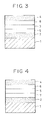
- FIG. 3 is a cross-sectional view of a further embodiment of a luminescent device in accordance with the present invention.
- FIG. 4 is a cross-sectional view of a luminescent device in accordance with Example 7 of the present invention.
- FIG. 5 is an infrared spectrum of an organic compound in accordance with the present invention.
- the present invention is characterized by a novel triarylamine compound represented by the general formula [1] or [2]:
- R 1 and R 2 are each independently a hydrogen atom, a halogen atom, a substituted or unsubstituted alkyl group, a substituted or unsubstituted alkoxy group, or a substituted or unsubstituted aryl group.
- alkyl groups include methyl, ethyl, n-propyl, and isopropyl groups
- examples of alkoxy groups include methoxy, ethoxy, and phenoxy groups
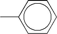
- examples of aryl groups include phenyl, biphenyl, and naphthyl groups.
- substituent groups include halogen atoms, e.g., fluorine, chlorine, bromine, and iodine; alkyl groups, e.g., methyl, ethyl, n-propyl, and iso-propyl groups; alkoxy groups, e.g., methoxy, ethoxy, and phenoxy groups; aralkyl groups, e.g., benzyl, phenetyl, and propylphenyl group; a nitro group; a cyano group; substituted amino groups, e.g., dimethyl amino, dibenzylamino, diphenylamino, and morpholino groups; aryl groups, e.g., phenyl, tolyl, biphenyl, naphthyl, anthryl, and pyrenyl groups; and heterocyclic groups, e.g., pyridyl, thienyl, furyl, quinoly,
- Ar 1 , Ar 2 , Ar 3 , and Ar 4 are each a substituted or unsubstituted aryl or heterocyclic group, which may be the same or different from each other.
- substituted or unsubstituted aryl groups include phenyl, biphenyl, terphenyl, naphthyl, anthryl, and fluorenyl.
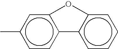
- substituted or unsubstituted heterocyclic groups include pyridyl, furyl, thienyl, and carbazolyl groups.
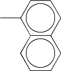
- At least one of Ar 1 , Ar 2 , Ar 3 , and Ar 4 is a fused aromatic ring.
- the fused aromatic rings include naphthyl, anthryl, acenaphthyl, phenanthryl, naphthanyl, and fluoranthenyl rings.
- These fused aromatic rings may have substituent groups.
- the substituent groups include halogen atoms, e.g., fluorine, chlorine, bromine, and iodine; alkyl groups, e.g.
- alkoxy groups e.g., methoxy, ethoxy, and phenoxy groups
- aralkyl groups e.g., benzyl, phenetyl, and propylphenyl group
- a nitro group e.g., a cyano group
- substituted amino groups e.g., dimethyl amino, dibenzylamino, diphenylamino, and morpholino groups
- aryl groups e.g., phenyl, tolyl, biphenyl, naphthyl, anthryl, and pyrenyl groups
- heterocyclic groups e.g., pyridyl, thienyl, furyl, quinolyl, and carbazolyl groups.
- R 3 and R 4 are the same as R 1 and R 2 , respectively, in the general formula [1]
- Ar 5 , Ar 6 , Ar 7 , and Ar 8 are the same as Ar 1 , Ar 2 , Ar 3 , and Ar 4 , respectively, in the general formula [1].
- At least one of Ar 5 , Ar 6 , Ar 7 , and Ar 8 is a ⁇ -conjugated aromatic hydrocarbon having 12 or more carbon atoms.
- Examples of the ⁇ -conjugated aromatic hydrocarbon having 12 or more carbon atoms include polyphenyls, i.e., biphenyl, p-terphenyl, and quaterphenyl; and stilbene derivatives, i.e., styryl and phenylstyryl.
- the luminescent device in accordance with the present invention has a layer or a plurality of layers composed of an organic compound disposed between an anode and a cathode, and at least one layer among the above organic layers contains a compound represented by the general formula [1] or [2].
- the layer of the organic compound represented by the general formula [1] or [2] is formed between the anode and the cathode by a vacuum deposition process or a solution coating process.
- the thickness of the organic layer is preferably 2 ⁇ m or less, and more preferably 0.5 ⁇ m or less, and most preferably 0.05 to 0.5 ⁇ m.
- FIG. 1 is a schematic cross-sectional view of an embodiment of the luminescent device in accordance with the present invention.
- An anode 2 , a luminescent layer 3 and a cathode 4 are formed on a substrate 1 , in that order.
- a usable luminescent layer 3 is generally composed of a single compound having hole transportability, electron transportability and luminescence, or a mixture of compounds each having one of these properties.
- FIG. 2 is a schematic cross-sectional view of another embodiment of the luminescent device in accordance with the present invention.
- An anode 2 , a hole transport layer 5 , an electron transport layer 6 and a cathode 4 are formed on a substrate 1 , in that order.
- the hole transport layer 5 and the electron transport layer 6 function as a luminescent layer 3 .
- a usable hole transport layer 5 is generally composed of a luminescent material having hole transportability or a mixture including such a material and a non-luminescent material having hole transportability.
- the luminescent and non-luminescent materials may also have electron transportability.
- the electron transport layer 6 may be composed of a luminescent material having electron transportability or a mixture including such a material and a non-luminescent material having electron transportability.
- the luminescent and non-luminescent materials may also have hole transportability.
- FIG. 3 is a schematic cross-sectional view of a further embodiment of the luminescent device in accordance with the present invention.
- An anode 2 , a hole transport layer 5 , a luminescent layer 3 , an electron transport layer 6 and a cathode 4 are formed on a substrate 1 in that order.
- carrier transport and luminescence are performed in the individual layers.
- Such a configuration permits a wide variety of combinations of a material having excellent hole transportability, a material having excellent electron transportability and a material having excellent luminescence.
- the configuration permits the use of various compounds emitting light at different wavelengths; hence the hue of the luminescent light can be controlled over a wide range. Effective trap of holes and electrons (or excimers) in the central luminescent layer will increase the luminescent efficiency.
- FIG. 4 is a cross-sectional view of another luminescent device in accordance with the present invention.
- An anode 2 , a hole injection-transport layer 7 , a hole transport layer 5 , an electron transport layer 6 , and a cathode 4 are formed on a substrate 1 , in that order.
- the hole injection-transport layer 7 facilitates hole injection from the anode 2 .
- the luminescent device can maintain high efficiency for long driving times.
- the hole transport layer 5 and/or the electron transport layer 6 function as a luminescent layer.
- the compounds represented by the general formulae [1] and [2] have significantly superior luminescent characteristics to conventional compounds and can be used in all the electric field luminescent devices shown in FIGS. 1 to 4 .
- the compounds represented by the general formulae [1] and [2] have hole transportability and/or electron transportability depending on the structures thereof.
- the compounds represented by the general formula [1] may be used alone or in combination, and the compounds represented by the general formula [2] may also be used alone or in combination.
- the compounds represented by the general formulae [1] and [2] may be used in combination.
- hole transport materials studied in the field of electrophotographic photosensitive members and known luminescent hole transport compounds as shown in Tables 1 to 5 or electron transport compounds and known luminescent electron transport materials as shown in Table 6 to 9 can be used with the compounds represented by the general formulae [1] and [2]. These compounds are used alone or in combination.
- Table 10 illustrates examples of dopant dyes. The addition of a trace amount of dopant dye in the luminescent layer will significantly increase the luminescent efficiency or will change the luminescent color.
- Electron Transport Compounds M Al, Ga M: Zn, Mg, Be M: Zn, Mg, Be M: Zn, Mg, Be M: Zn, Mg, Be
- the luminescent layer containing the compounds represented by the general formulae [1] and [2] and the other organic layer are generally formed by a vacuum deposition process or using a binding resin.
- Non-limiting examples of the binding resins include polyvinyl carbazole resins, polycarbonate resins, polyester resins, polyarylate resins, butyral resins, polystyrene resins, polyvinyl acetal resins, diallyl phthalate resins, acrylic resins, methacrylic resins, phenol resins, epoxy resins, silicon resins, polysulfone resins, and urea resins. These binding resins can be used alone or in combination.
- Preferable anode materials have large work functions. Examples of such materials include nickel, gold, platinum, palladium, selenium, rhenium, and iridium; alloys thereof; and tin oxide, indium tin oxide, and copper iodide.
- Conductive polymers such as poly(3-methylthiophene), polyphenylene sulfide and polypyrrole are also usable.
- preferable cathode materials have small work functions.
- examples of such materials include silver, lead, tin, magnesium, aluminum, calcium, manganese, indium and chromium, and alloys thereof.
- At least one electrode of the anode and cathode transmits 50% or more of incident light over the wavelength region of the luminescent light.
- transparent substrate glass and plastic films are used in the present invention.
- FIG. 5 is an IR spectrum of the compound by a KBr tablet method using an FT-IR spectrophotometer (FT-IR-420) by JASCO.
- ITO indium tin oxide
- a layer of Compound 12 with a thickness of 65 nm was deposited thereon at a deposition rate of 0.2 to 0.3 nm/sec.
- a 65 nm thick aluminum quinolinol film was formed.
- a direct current of 10 V was applied between the ITO anode and the Mg—Ag cathode of the luminescent device.
- a current flow of 175 mA/cm 2 and a green luminescence with a luminance of 5,300 cd/m 2 were observed.
- a voltage with a current density of 3.0 mA/cm 2 was applied to the sample for 100 hours. The luminance was 160 cd/m 2 at the start and changed to 140 cd/m 2 at the end.
- Luminescent devices were prepared as in EXAMPLE 1 using Compounds 21, 36, 47, 72 and 88 instead of Compound 12. Table 11 shows the characteristics of these luminescent devices.
- a luminescent device was prepared as in EXAMPLE 1 using the following compound instead of Compound 12.
- a direct current of 15 V was applied between the ITO anode and the Mg—Ag cathode of the luminescent device.
- a current flow of 15 mA/cm 2 and a green luminescence with a luminance of 35 cd/m 2 were observed.
- a voltage with a current density of 27 mA/cm 2 was applied to the sample for 100 hours. The luminance was 100 cd/m 2 at the start and decreased to 8 cd/m 2 at the end.
- a luminescent device shown in FIG. 4 was prepared as follows.
- An indium tin oxide (ITO) anode 2 with a thickness of 100 nm was formed on a glass substrate by a sputtering process.
- a m-MTDATA hole injection-transport layer 7 with a thickness of 20 nm was formed thereon, and a layer of Compound 32 with a thickness of 50 nm was deposited thereon as a hole transport layer 5 .
- an electron transport layer of an electron transport compound (Alq 3 ) with a thickness of 65 nm was formed thereon, and then an aluminum cathode 4 with a thickness of 140 nm was formed thereon.
- a direct current of 5 V was applied between the ITO anode and the aluminum cathode of the luminescent device.
- a current flow of 10 mA/cm 2 and a green luminescence with a luminance of 576 cd/m 2 were observed.
- a voltage with a current density of 3.0 mA/cm 2 was applied to the sample for 100 hours. The luminance was 265 cd/m 2 at the start and slightly changed to 250 cd/m 2 at the end.
- luminescent devices using compounds represented by the general formulae [1] and [2] in accordance with the present invention have significantly high luminance for a low applied-voltage, and high durability.
- a large device can be readily formed by a vacuum deposition process or a casting process with relatively low production costs.
Abstract
A luminescent device having a pair of electrodes and a luminescent layer disposed between the electrodes. The luminescent layer comprises a compound represented by the following general formula: 
Description
This application is a continuation-in-part of application Ser. No. 09/299,632, filed on Apr. 27, 1999, now abandoned, which is incorporated by reference herein.
1. Field of the Invention
The present invention relates to a novel triarylamine compound and to a charge-injection-type luminescent device using the same. In particular, the present invention relates to a triarylamine compound applicable to a charge-injection-type luminescent device which directly converts injected charges into optical energy by an applied electric field, and relates to a luminescent device using the same.
2. Description of the Related Art
Pope et al., first discovered electroluminescence (EL) in an organic material, that is, single-crystal anthracene in 1963 (J. Chem. Phys., 38, 2042 (1963)). Subsequently, Helfinch and Schneider observed relatively strong EL in an injection EL material containing a solution system having a high injection efficiency in 1965 (Phys. Rev. Lett., 14, 229 (1965)).
Many studies of organic luminescent materials containing conjugated organic hosts and conjugated organic activators having condensed benzene rings have been disclosed in U.S. Pat. Nos. 3,172,862, 3,173,050, and 3,710,167; J. Chem. Phys., 44, 2902 (1966); J. Chem. Phys., 58, 1542 (1973); and Chem. Phys. Lett., 36, 345 (1975). Examples of disclosed organic hosts include naphthalene, anthracene, phenanthrene, tetracene, pyrene, benzpyrene, chrysene, picene, carbazole, fluorene, biphenyl, terphenyl, triphenylene oxide, dihalobiphenyl, trans-stilbene, and 1,4-diphenylbutadiene. Examples of disclosed activators include anthracene, tetracene and pentacene. Since these organic luminescent materials are provided as single layers having a thickness of more than 1 μm, a high electric field is required for luminescence. Under these circumstances, thin film devices formed by a vacuum deposition process have been proposed (for example, “Thin Solid Films” p. 94 (1982); Polymer, 24, 748 (1983); and J. Appl. Phys., 25, L773 (1986)). Although the thin film devices are effective for reducing the driving voltage, their luminance is far from levels for practical use.
In recent years, Tang, et al., have developed an EL device having a high luminance at a low driving voltage (Appl. Phys. Lett., 51, 913 (1987) and U.S. Pat. No. 4,356,429). The EL device is fabricated by depositing two significantly thin layers, that is, a charge transport layer and a luminescent layer, between the anode and the cathode by a vacuum deposition process. Such layered organic EL devices are disclosed in, for example, Japanese Patent Application Laid-Open Nos. 59-194393, 59-194393, 63-264692, and 3-163188, U.S. Pat. Nos. 4,539,507 and 4,720,432, and Appl. Phys. Lett., 55, 1467 (1989).
Also, an EL device of a triple-layered structure having independently a carrier transport function and a luminescent ability was disclosed in Jpn. J. Apply. Phys., 27, L269 and L713 (1988). Since the carrier transportability is improved in such an EL device, the versatility of possible dyes in the luminescent layer is considerably increased. Further, the device configuration suggests feasibility of improved luminescence by effectively trapping holes and electrons (or excimers) in the central luminescent layer.
Layered organic EL devices are generally formed by vacuum deposition processes. EL devices having considerable luminance are also formed by casting processes (as described in, for example, Extended Abstracts (The 50th Autumn Meeting (1989), p. 1006 and The 51st Autumn Meeting (1990), p. 1041; The Japan Society of Applied Physics). Considerably high luminance is also achieved by a single-layered mixture-type EL device, in which the layer is formed by immersion-coating a solution containing polyvinyl carbazole as a hole transport compound, an oxadiazole derivative as an electron transport compound and coumarin-6 as a luminescent material, as described in Extended Abstracts of the 38th Spring Meeting 1991, p. 1086; The Japan Society of Applied Physics and Related Societies.
As described above, the organic EL devices have been significantly improved and have suggested the feasibility of a wide variety of applications; however, these EL devices have some problems in practical use, for example, insufficient luminance, changes in luminance during prolonged use, and deterioration by atmospheric gas containing oxygen and humidity. Further, the EL devices do not sufficiently satisfy needs for diverse wavelengths of luminescent light for precisely determining luminescent hues of blue, green and red colors in full-color displays, etc.
It is an object of the present invention to provide an organic compound applicable to a luminescent device having an optical output with significantly high efficiency and luminance.
It is another object of the present invention to provide an organic compound applicable to a luminescent device, which has diverse luminescent wavelengths, a variety of luminescent hues, and significantly high durability.
It is a further object of the present invention to provide a luminescent device easily produced at relatively low production cost and is highly safe.
An aspect of the present invention is a triarylamine compound represented by the following general formula [1]: 
wherein R1 and R2 are each independently a hydrogen atom, a halogen atom, a substituted or unsubstituted alkyl group, a substituted or unsubstituted alkoxy group, or a substituted or unsubstituted aryl group; Ar1, Ar2, Ar3, and Ar4 are each a substituted or unsubstituted aryl or heterocyclic group, which may be the same or different from each other; and at least one of Ar1, Ar2, Ar3, and Ar4 is a fused aromatic ring.
Another aspect of the present invention is a triarylamine compound represented by the following general formula [2]: 
wherein R3 and R4 are each independently a hydrogen atom, a halogen atom, a substituted or unsubstituted alkyl group, a substituted or unsubstituted alkoxy group, or a substituted or unsubstituted aryl group; Ar5, Ar6, Ar7, and Ar8 are each a substituted or unsubstituted aryl or heterocyclic group, which may be the same or different from each other; and at least one of Ar5, Ar6, Ar7, and Ar8 is a π-conjugated aromatic hydrocarbon having 12 or more carbon atoms.
A further aspect of the present invention is a luminescent device comprising a pair of electrodes, and at least one compound among the compounds represented by the general formulae [1] or [2] disposed therebetween.
The organic luminescent device in accordance with the present invention is a thin lightweight solid device having a large area and high resolution and capable of high-speed operation, unlike conventional incandescent lamps, fluorescent lamps, and inorganic luminescent diodes, and thus satisfies advanced requirements.
FIG. 1 is a cross-sectional view of an embodiment of a luminescent device in accordance with the present invention;
FIG. 2 is a cross-sectional view of another embodiment of a luminescent device in accordance with the present invention;
FIG. 3 is a cross-sectional view of a further embodiment of a luminescent device in accordance with the present invention;
FIG. 4 is a cross-sectional view of a luminescent device in accordance with Example 7 of the present invention; and
FIG. 5 is an infrared spectrum of an organic compound in accordance with the present invention.
The present invention is characterized by a novel triarylamine compound represented by the general formula [1] or [2]: 
In the general formula [1], R1 and R2 are each independently a hydrogen atom, a halogen atom, a substituted or unsubstituted alkyl group, a substituted or unsubstituted alkoxy group, or a substituted or unsubstituted aryl group.
Examples of alkyl groups include methyl, ethyl, n-propyl, and isopropyl groups; examples of alkoxy groups include methoxy, ethoxy, and phenoxy groups; and examples of aryl groups include phenyl, biphenyl, and naphthyl groups.
Examples of the substituent groups include halogen atoms, e.g., fluorine, chlorine, bromine, and iodine; alkyl groups, e.g., methyl, ethyl, n-propyl, and iso-propyl groups; alkoxy groups, e.g., methoxy, ethoxy, and phenoxy groups; aralkyl groups, e.g., benzyl, phenetyl, and propylphenyl group; a nitro group; a cyano group; substituted amino groups, e.g., dimethyl amino, dibenzylamino, diphenylamino, and morpholino groups; aryl groups, e.g., phenyl, tolyl, biphenyl, naphthyl, anthryl, and pyrenyl groups; and heterocyclic groups, e.g., pyridyl, thienyl, furyl, quinolyl, and carbazolyl groups.
In the general formula [1], Ar1, Ar2, Ar3, and Ar4 are each a substituted or unsubstituted aryl or heterocyclic group, which may be the same or different from each other. Examples of the substituted or unsubstituted aryl groups include phenyl, biphenyl, terphenyl, naphthyl, anthryl, and fluorenyl. Examples of the substituted or unsubstituted heterocyclic groups include pyridyl, furyl, thienyl, and carbazolyl groups.
At least one of Ar1, Ar2, Ar3, and Ar4 is a fused aromatic ring. Examples of the fused aromatic rings include naphthyl, anthryl, acenaphthyl, phenanthryl, naphthanyl, and fluoranthenyl rings. These fused aromatic rings may have substituent groups. Examples of the substituent groups include halogen atoms, e.g., fluorine, chlorine, bromine, and iodine; alkyl groups, e.g. methyl, ethyl, n-propyl, and iso-propyl groups; alkoxy groups, e.g., methoxy, ethoxy, and phenoxy groups; aralkyl groups, e.g., benzyl, phenetyl, and propylphenyl group; a nitro group; a cyano group; substituted amino groups, e.g., dimethyl amino, dibenzylamino, diphenylamino, and morpholino groups; aryl groups, e.g., phenyl, tolyl, biphenyl, naphthyl, anthryl, and pyrenyl groups; and heterocyclic groups, e.g., pyridyl, thienyl, furyl, quinolyl, and carbazolyl groups. 
In the general formula [2], R3 and R4 are the same as R1 and R2, respectively, in the general formula [1], and Ar5, Ar6, Ar7, and Ar8 are the same as Ar1, Ar2, Ar3, and Ar4, respectively, in the general formula [1]. At least one of Ar5, Ar6, Ar7, and Ar8 is a π-conjugated aromatic hydrocarbon having 12 or more carbon atoms. Examples of the π-conjugated aromatic hydrocarbon having 12 or more carbon atoms include polyphenyls, i.e., biphenyl, p-terphenyl, and quaterphenyl; and stilbene derivatives, i.e., styryl and phenylstyryl.
The following are typical non-limiting examples of the compounds represented by the general formula [1] or [2].
Compounds represented by the general formula [1]
| Compound | Ar1 | Ar2 | ||
| No. | R1 | R2 | Ar3 | Ar4 |
| 1 | —H | —H |
 |
 |
 |
 |
|||
| 2 | —H | —H |
 |
 |
 |
 |
|||
| 3 | —H | —H |
 |
 |
 |
 |
|||
| 4 | —H | —H |
 |
 |
 |
 |
|||
| 5 | —H | —H |
 |
 |
 |
 |
|||
| 6 | —H | —H |
 |
 |
 |
 |
|||
| 7 | —H | —H |
 |
 |
 |
 |
|||
| 8 | —H | —CH3 |
 |
 |
 |
 |
|||
| 9 | —H |
 |
 |
 |
 |
 |
|||
| 10 | —H | —Br |
 |
 |
 |
 |
|||
| 11 | —CH3 | —CH3 |
 |
 |
 |
 |
|||
| 12 | —CH3 | —CH3 |
 |
 |
 |
 |
|||
| 13 | —CH3 | —CH3 |
 |
 |
 |
 |
|||
| 14 | —CH3 | —CH3 |
 |
 |
 |
 |
|||
| 15 | —CH3 | —CH3 |
 |
 |
 |
 |
|||
| 16 | —CH3 | —CH3 |
 |
 |
 |
 |
|||
| 17 | —CH3 | —CH3 |
 |
 |
 |
 |
|||
| 18 | —CH3 | —CH3 |
 |
 |
 |
 |
|||
| 19 | —CH3 | —CH3 |
 |
 |
 |
 |
|||
| 20 | —CH3 | —CH3 |
 |
 |
 |
 |
|||
| 21 | —CH3 | —CH3 |
 |
 |
 |
 |
|||
| 22 | —CH3 | —CH3 |
 |
 |
 |
 |
|||
| 23 | —CH3 | —CH3 |
 |
 |
 |
 |
|||
| 24 | —CH3 | —CH3 |
 |
 |
 |
 |
|||
| 25 | —CH3 | —CH3 |
 |
 |
 |
 |
|||
| 26 | —CH3 | —CH3 |
 |
 |
 |
 |
|||
| 27 | —CH3 | —CH3 |
 |
 |
 |
 |
|||
| 28 | —CH3 | —CH3 |
 |
 |
 |
 |
|||
| 29 | —CH3 | —CH3 |
 |
 |
 |
 |
|||
| 30 | —CH3 | —CH3 |
 |
 |
 |
 |
|||
| 31 | —C2H5 | —C2H5 |
 |
 |
 |
 |
|||
| 32 | —C2H5 | —C2H5 |
 |
 |
 |
 |
|||
| 33 | —C2H5 | —C2H5 |
 |
 |
 |
 |
|||
| 34 | —C2H5 | —C2H5 |
 |
 |
 |
 |
|||
| 35 | —C2H5 | —C2H5 |
 |
 |
 |
 |
|||
| 36 | —C3H7 | —C3H7 |
 |
 |
 |
 |
|||
| 37 | —C3H7 | —CH3 |
 |
 |
 |
 |
|||
| 38 | —C3H7 |
 |
 |
 |
 |
 |
|||
| 39 | —C4H9 | —C4H9 |
 |
 |
 |
 |
|||
| 40 | —C4H9 | —C4H9 |
 |
 |
 |
 |
|||
| 41 | —C4H8 | —C4H8 |
 |
 |
| OCH3 | OCH3 |
 |
 |
|
| 42 | —C8H17 | —C8H17 |
 |
 |
 |
 |
|||
| 43 | —C8H17 | —C8H17 |
 |
 |
 |
 |
|||
| 44 | —C8H17 | —C8H17 |
 |
 |
 |
 |
|||
| 45 | —C18H37 | —C18H37 |
 |
 |
 |
 |
|||
Compounds represented by the general formula [2]
| Com- | ||||
| pound | Ar5 | Ar6 | ||
| No. | R3 | R4 | Ar7 | Ar8 |
| 46 | —C2H5 | —C2H5 |
 |
 |
 |
 |
|||
| 47 | —C2H5 | —C2H5 |
 |
 |
 |
 |
|||
| 48 | —C2H5 | —C2H5 |
 |
 |
 |
 |
|||
| 49 | —C2H5 | —C2H5 |
 |
 |
 |
 |
|||
| 50 | —C2H5 | —C2H5 |
 |
 |
 |
 |
|||
| 51 | —C3H7 | —C3H7 |
 |
 |
 |
 |
|||
| 52 | —CH3 | —C3H7 |
 |
 |
 |
 |
|||
| 53 | —C3H7 |
 |
 |
 |
 |
 |
|||
| 54 | —C4H9 | —C4H9 |
 |
 |
 |
 |
|||
| 55 | —C4H9 | —C4H9 |
 |
 |
 |
 |
|||
| 56 |
 |
 |
 |
 |
 |
 |
|||
| 57 | —C8H17 | —C8H17 |
 |
 |
 |
 |
|||
| 58 | —C8H17 | —C8H17 |
 |
 |
 |
 |
|||
| 59 | —C8H17 | —C8H17 |
 |
 |
 |
 |
|||
| 60 | —C18H37 | —C18H37 |
 |
 |
 |
 |
|||
| 61 | —CH3 | —CH3 |
 |
 |
 |
 |
|||
| 62 | —CH3 | —CH3 |
 |
 |
 |
 |
|||
| 63 | —CH3 | —CH3 |
 |
 |
 |
 |
|||
| 64 | —CH3 | —CH3 |
 |
 |
 |
 |
|||
| 65 | —CH3 | —CH3 |
 |
 |
 |
 |
|||
| 66 | —CH3 | —CH3 |
 |
 |
 |
 |
|||
| 67 | —CH3 | —CH3 |
 |
 |
 |
 |
|||
| 68 | —CH3 | —CH3 |
 |
 |
 |
 |
|||
| 69 | —CH3 | —CH3 |
 |
 |
 |
 |
|||
| 70 | —CH3 | —CH3 |
 |
 |
 |
 |
|||
| 71 | —CH3 | —CH3 |
 |
 |
 |
 |
|||
| 72 | —CH3 | —CH3 |
 |
 |
 |
 |
|||
| 73 | —CH3 | —CH3 |
 |
 |
 |
 |
|||
| 74 | —CH3 | —CH3 |
 |
 |
 |
 |
|||
| 75 | —CH3 | —CH3 |
 |
 |
 |
 |
|||
| 76 | —H | —H |
 |
 |
 |
 |
|||
| 77 | —H | —H |
 |
 |
 |
 |
|||
| 78 | —H | —H |
 |
 |
 |
 |
|||
| 79 | —H | —H |
 |
 |
 |
 |
|||
| 80 | —H | —H |
 |
 |
 |
 |
|||
| 81 | —H | —H |
 |
 |
 |
 |
|||
| 82 | —H | —CH3 |
 |
 |
 |
 |
|||
| 83 | —H | —C3H7 |
 |
 |
 |
 |
|||
| 84 | —H |
 |
 |
 |
 |
 |
|||
| 85 | —H | —Br |
 |
 |
 |
 |
|||
| 86 | —CH3 | —CH3 |
 |
 |
 |
 |
|||
| 87 | —CH3 | —CH3 |
 |
 |
 |
 |
|||
| 88 | —CH3 | —CH3 |
 |
 |
 |
 |
|||
| 89 | —CH3 | —C3H7 |
 |
 |
 |
 |
|||
| 90 | —CH3 | —C3H7 |
 |
 |
 |
 |
|||
The luminescent device in accordance with the present invention has a layer or a plurality of layers composed of an organic compound disposed between an anode and a cathode, and at least one layer among the above organic layers contains a compound represented by the general formula [1] or [2].
The layer of the organic compound represented by the general formula [1] or [2] is formed between the anode and the cathode by a vacuum deposition process or a solution coating process. The thickness of the organic layer is preferably 2 μm or less, and more preferably 0.5 μm or less, and most preferably 0.05 to 0.5 μm.
The present invention will now be described in further detail with reference to the drawings.
FIG. 1 is a schematic cross-sectional view of an embodiment of the luminescent device in accordance with the present invention. An anode 2, a luminescent layer 3 and a cathode 4 are formed on a substrate 1, in that order. In such a configuration, a usable luminescent layer 3 is generally composed of a single compound having hole transportability, electron transportability and luminescence, or a mixture of compounds each having one of these properties.
FIG. 2 is a schematic cross-sectional view of another embodiment of the luminescent device in accordance with the present invention. An anode 2, a hole transport layer 5, an electron transport layer 6 and a cathode 4 are formed on a substrate 1, in that order. The hole transport layer 5 and the electron transport layer 6 function as a luminescent layer 3. In such a configuration, a usable hole transport layer 5 is generally composed of a luminescent material having hole transportability or a mixture including such a material and a non-luminescent material having hole transportability. The luminescent and non-luminescent materials may also have electron transportability. The electron transport layer 6 may be composed of a luminescent material having electron transportability or a mixture including such a material and a non-luminescent material having electron transportability. The luminescent and non-luminescent materials may also have hole transportability.
FIG. 3 is a schematic cross-sectional view of a further embodiment of the luminescent device in accordance with the present invention. An anode 2, a hole transport layer 5, a luminescent layer 3, an electron transport layer 6 and a cathode 4 are formed on a substrate 1 in that order. In this configuration, carrier transport and luminescence are performed in the individual layers. Such a configuration permits a wide variety of combinations of a material having excellent hole transportability, a material having excellent electron transportability and a material having excellent luminescence. Further, the configuration permits the use of various compounds emitting light at different wavelengths; hence the hue of the luminescent light can be controlled over a wide range. Effective trap of holes and electrons (or excimers) in the central luminescent layer will increase the luminescent efficiency.
FIG. 4 is a cross-sectional view of another luminescent device in accordance with the present invention. An anode 2, a hole injection-transport layer 7, a hole transport layer 5, an electron transport layer 6, and a cathode 4 are formed on a substrate 1, in that order. The hole injection-transport layer 7 facilitates hole injection from the anode 2. Thus, the luminescent device can maintain high efficiency for long driving times. In such a configuration, the hole transport layer 5 and/or the electron transport layer 6 function as a luminescent layer.
The compounds represented by the general formulae [1] and [2] have significantly superior luminescent characteristics to conventional compounds and can be used in all the electric field luminescent devices shown in FIGS. 1 to 4.
The compounds represented by the general formulae [1] and [2] have hole transportability and/or electron transportability depending on the structures thereof. In all the embodiments shown in FIGS. 1 to 4, the compounds represented by the general formula [1] may be used alone or in combination, and the compounds represented by the general formula [2] may also be used alone or in combination. Alternatively, the compounds represented by the general formulae [1] and [2] may be used in combination.
As components of the luminescent layer in the luminescent device in accordance with the present invention, hole transport materials studied in the field of electrophotographic photosensitive members and known luminescent hole transport compounds as shown in Tables 1 to 5 or electron transport compounds and known luminescent electron transport materials as shown in Table 6 to 9 can be used with the compounds represented by the general formulae [1] and [2]. These compounds are used alone or in combination.
Table 10 illustrates examples of dopant dyes. The addition of a trace amount of dopant dye in the luminescent layer will significantly increase the luminescent efficiency or will change the luminescent color.
| TABLE 1 |
| Hole Transport Compounds |
 |
 |
 |
 |
 |
 |
| TABLE 2 |
| Hole Transport Compounds |
 |
 |
 |
 |
 |
| TABLE 3 |
| Hole Transport Compounds |
 |
| TABLE 4 |
| Hole Transport Compounds |
 |
 |
 |
 |
 |
||
 |
 |
||
| TABLE 5 |
| Hole Transport Compounds |
 |
 |
| TABLE 6 |
| Electron Transport Compounds |
 |
 |
| M: Al, Ga | M: Zn, Mg, Be |
 |
 |
| M: Zn, Mg, Be | M: Zn, Mg, Be |
| TABLE 7 |
| Electron Transport Compounds |
 |
 |
 |
 |
| TABLE 8 |
| Electron Transport Compounds |
 |
 |
 |
 |
| TABLE 9 |
| Electron Transport Compounds |
 |
 |
 |
 |
 |
 |
| TABLE 10 |
| Dopant Dyes |
 |
 |
 |
 |
 |
 |
 |
|
In the luminescent device in accordance with the present invention, the luminescent layer containing the compounds represented by the general formulae [1] and [2] and the other organic layer are generally formed by a vacuum deposition process or using a binding resin.
Non-limiting examples of the binding resins include polyvinyl carbazole resins, polycarbonate resins, polyester resins, polyarylate resins, butyral resins, polystyrene resins, polyvinyl acetal resins, diallyl phthalate resins, acrylic resins, methacrylic resins, phenol resins, epoxy resins, silicon resins, polysulfone resins, and urea resins. These binding resins can be used alone or in combination.
Preferable anode materials have large work functions. Examples of such materials include nickel, gold, platinum, palladium, selenium, rhenium, and iridium; alloys thereof; and tin oxide, indium tin oxide, and copper iodide. Conductive polymers, such as poly(3-methylthiophene), polyphenylene sulfide and polypyrrole are also usable.
In contrast, preferable cathode materials have small work functions. Examples of such materials include silver, lead, tin, magnesium, aluminum, calcium, manganese, indium and chromium, and alloys thereof.
It is preferable that at least one electrode of the anode and cathode transmits 50% or more of incident light over the wavelength region of the luminescent light.
As the transparent substrate, glass and plastic films are used in the present invention.
The present invention is described in further detail with reference to the following examples.
Synthesis of N,N,N′,N′-tetra-(1-naphthyl)-2,7-diamino-9,9-dimethylfluorene (Compound 13)
Into a 100-ml egg-plant type flask, 2.24 g (10 mmol) of 2,7-diamino-9,9-dimethylfluorene, 15.22 g (160 mmol) of 1-iodonaphthalene, 6.91 g(50 mmol) of potassium carbonate, 12.71 g (200 mmol) of powdered copper, and 50 ml of o-dichlorobenzene were fed, and the mixture was refluxed with stirring for 24 hours.
The reactant solution was cooled and then filtered, and the filtrate was concentrated under reduced pressure. Into the concentrated solution, 35 ml of acetone was added and then filtered to collect precipitated crude crystal. The crude crystal was purified through a silica gel column using a toluene-hexane mixture, and 6.13 g (yield: 84.1%) of pale yellow fine crystal N,N,N′,N′-tetra-(1-naphthyl)-2,7-diamino-9,9-dimethylfluorene (Compound 13) was prepared.
The melting point (Tm) and the glass transition temperature (Tg) of the resulting compound were 331.0 to 332.7° C. and 169° C., respectively, according to differential scanning calorimetry using Pyris 1 by Perkin Elmer Corporation. FIG. 5 is an IR spectrum of the compound by a KBr tablet method using an FT-IR spectrophotometer (FT-IR-420) by JASCO.
An indium tin oxide (ITO) film with a thickness of 100 nm was formed on a glass substrate by a sputtering process. After the transparent substrate was cleaned, a layer of Compound 12 with a thickness of 65 nm was deposited thereon at a deposition rate of 0.2 to 0.3 nm/sec. Then, a 65 nm thick aluminum quinolinol film was formed. Thereafter, a Mg—Ag metallic electrode having an atomic ratio of Mg:Ag=10:1 was formed by a vacuum deposition process at a deposition rate of 2.0 nm/sec under a vacuum pressure of 3 to 4×10⁻⁶ torr. A luminescent device was thereby formed.
A direct current of 10 V was applied between the ITO anode and the Mg—Ag cathode of the luminescent device. A current flow of 175 mA/cm2 and a green luminescence with a luminance of 5,300 cd/m2 were observed. A voltage with a current density of 3.0 mA/cm2 was applied to the sample for 100 hours. The luminance was 160 cd/m2 at the start and changed to 140 cd/m2 at the end.
Luminescent devices were prepared as in EXAMPLE 1 using Compounds 21, 36, 47, 72 and 88 instead of Compound 12. Table 11 shows the characteristics of these luminescent devices.
| TABLE 11 | |||
| Initial | After 100 hours | ||
| Applied | Applied | ||||
| Com- | Voltage | Luminance | Voltage | Luminance | |
| EXAMPLE | pound | (V) | (cd/m2) | (V) | (cd/m2) |
| 2 | 21 | 5.3 | 350 | 5.9 | 345 |
| 3 | 36 | 6.7 | 275 | 7.8 | 280 |
| 4 | 47 | 4.8 | 345 | 5.7 | 330 |
| 5 | 72 | 4.9 | 550 | 5.5 | 530 |
| 6 | 88 | 5.7 | 450 | 3.8 | 450 |
A luminescent device was prepared as in EXAMPLE 1 using the following compound instead of Compound 12. 
A direct current of 15 V was applied between the ITO anode and the Mg—Ag cathode of the luminescent device. A current flow of 15 mA/cm2 and a green luminescence with a luminance of 35 cd/m2 were observed. A voltage with a current density of 27 mA/cm2 was applied to the sample for 100 hours. The luminance was 100 cd/m2 at the start and decreased to 8 cd/m2 at the end.
The results of EXAMPLES 1 to 6 and COMPARATIVE EXAMPLE 1 show that the compounds in accordance with the present invention have high luminance and prolonged life compared to the comparative amine compound.
A luminescent device shown in FIG. 4 was prepared as follows. An indium tin oxide (ITO) anode 2 with a thickness of 100 nm was formed on a glass substrate by a sputtering process. After the transparent substrate was cleaned, a m-MTDATA hole injection-transport layer 7 with a thickness of 20 nm was formed thereon, and a layer of Compound 32 with a thickness of 50 nm was deposited thereon as a hole transport layer 5. Furthermore, an electron transport layer of an electron transport compound (Alq3) with a thickness of 65 nm was formed thereon, and then an aluminum cathode 4 with a thickness of 140 nm was formed thereon. 
A direct current of 5 V was applied between the ITO anode and the aluminum cathode of the luminescent device. A current flow of 10 mA/cm2 and a green luminescence with a luminance of 576 cd/m2 were observed. A voltage with a current density of 3.0 mA/cm2 was applied to the sample for 100 hours. The luminance was 265 cd/m2 at the start and slightly changed to 250 cd/m2 at the end.
As described above, luminescent devices using compounds represented by the general formulae [1] and [2] in accordance with the present invention have significantly high luminance for a low applied-voltage, and high durability. A large device can be readily formed by a vacuum deposition process or a casting process with relatively low production costs.
While the present invention has been described with reference to what are presently considered to be the preferred embodiments, it is to be understood that the invention is not limited to the disclosed embodiments. On the contrary, the invention is intended to cover various modifications and equivalent arrangements included within the spirit and scope of the appended claims. The scope of the following claims is to be accorded the broadest interpretation so as to encompass all such modifications and equivalent structures and functions.
Claims (3)
1. A luminescent device comprising a pair of electrodes and a luminescent layer disposed therebetween, wherein the luminescent layer comprises a compound of formula (12): 
2. A luminescent device comprising a pair of electrodes and a luminescent layer disposed therebetween, wherein the luminescent layer comprises a compound of formula (13): 
3. A luminescent device comprising a pair of electrodes and a luminescent layer disposed therebetween, the luminescent layer comprises a compound represented by the following general formula (1) and a compound represented by the following general formula (2): 
wherein R1 and R2 are each independently a hydrogen atom, a halogen atom, substituted or unsubstituted alkyl group, a substituted or unsubstituted alkoxy group, or a substituted or unsubstituted aryl group; Ar1, Ar2, Ar3, and Ar4 are each a substituted or unsubstituted aryl or heterocyclic group, which may be the same or different from each other; both Ar1 and Ar3 are fused aromatic rings; and at least one of R1 and R2 is a hydrogen, a halogen, a substituted or unsubstituted alkyl group, or a substituted or unsubstituted alkoxy group; and 
wherein R3 and R4 are each independently a hydrogen atom, a halogen atom, a substituted or unsubstituted alkyl group, a substituted or unsubstituted alkoxy group, or a substituted or unsubstituted aryl group; Ar5, Ar6, Ar7, and Ar8 are each a substituted or unsubstituted aryl or heterocyclic group, which may be the same or different from each other; at least one of Ar5, Ar6, Ar7, and Ar8 is a π-conjugated aromatic hydrocarbon having 12 or more carbon atoms selected from the group consisting of a polyphenyl and a stilbene; and at least one of R3 and R4 is a halogen, a substituted or unsubstituted alkyl group, or a substituted or unsubstituted alkoxy group.
Priority Applications (2)
| Application Number | Priority Date | Filing Date | Title |
|---|---|---|---|
| US10/348,990 US6833200B2 (en) | 1998-04-28 | 2003-01-23 | Luminescent device with a triarylamine compound |
| US10/921,918 US20050025997A1 (en) | 1998-04-28 | 2004-08-20 | Luminescent device with a triarylamine compound |
Applications Claiming Priority (5)
| Application Number | Priority Date | Filing Date | Title |
|---|---|---|---|
| JP132636/1998 | 1998-04-28 | ||
| JP13263698 | 1998-04-28 | ||
| JP10-132636 | 1998-04-28 | ||
| US29963299A | 1999-04-27 | 1999-04-27 | |
| US10/348,990 US6833200B2 (en) | 1998-04-28 | 2003-01-23 | Luminescent device with a triarylamine compound |
Related Parent Applications (1)
| Application Number | Title | Priority Date | Filing Date |
|---|---|---|---|
| US29963299A Continuation-In-Part | 1998-04-28 | 1999-04-27 |
Related Child Applications (1)
| Application Number | Title | Priority Date | Filing Date |
|---|---|---|---|
| US10/921,918 Division US20050025997A1 (en) | 1998-04-28 | 2004-08-20 | Luminescent device with a triarylamine compound |
Publications (2)
| Publication Number | Publication Date |
|---|---|
| US20030207153A1 US20030207153A1 (en) | 2003-11-06 |
| US6833200B2 true US6833200B2 (en) | 2004-12-21 |
Family
ID=29272132
Family Applications (2)
| Application Number | Title | Priority Date | Filing Date |
|---|---|---|---|
| US10/348,990 Expired - Fee Related US6833200B2 (en) | 1998-04-28 | 2003-01-23 | Luminescent device with a triarylamine compound |
| US10/921,918 Abandoned US20050025997A1 (en) | 1998-04-28 | 2004-08-20 | Luminescent device with a triarylamine compound |
Family Applications After (1)
| Application Number | Title | Priority Date | Filing Date |
|---|---|---|---|
| US10/921,918 Abandoned US20050025997A1 (en) | 1998-04-28 | 2004-08-20 | Luminescent device with a triarylamine compound |
Country Status (1)
| Country | Link |
|---|---|
| US (2) | US6833200B2 (en) |
Cited By (8)
| Publication number | Priority date | Publication date | Assignee | Title |
|---|---|---|---|---|
| US20050025997A1 (en) * | 1998-04-28 | 2005-02-03 | Canon Kabushiki Kaisha | Luminescent device with a triarylamine compound |
| US20050221125A1 (en) * | 1999-12-15 | 2005-10-06 | Yukiko Morioka | Organic electroluminescence device |
| US20080124573A1 (en) * | 2006-11-28 | 2008-05-29 | Canon Kabushiki Kaisha | Amine compound and organic light-emitting device |
| US20080309229A1 (en) * | 2005-12-22 | 2008-12-18 | Cambridge Display Technology Limited | Arylamine Polymer |
| US20090091244A1 (en) * | 2005-12-20 | 2009-04-09 | Canon Kabushiki Kaisha | Amine compound, organic light-emitting device, and organic blue-light-emitting device |
| US10861903B2 (en) | 2017-08-07 | 2020-12-08 | Canon Kabushiki Kaisha | Organic compound and photoelectric conversion element |
| US10873032B2 (en) | 2016-03-03 | 2020-12-22 | Canon Kabushiki Kaisha | Organic photoelectric conversion element, two-dimensional sensor, image sensor, and imaging apparatus |
| US11895910B2 (en) | 2017-08-23 | 2024-02-06 | Canon Kabushiki Kaisha | Organic compound and photoelectric conversion element |
Families Citing this family (7)
| Publication number | Priority date | Publication date | Assignee | Title |
|---|---|---|---|---|
| US6682832B2 (en) * | 1999-12-20 | 2004-01-27 | Matsushita Electric Industrial Co., Ltd. | Thin film el device |
| KR101217899B1 (en) * | 2003-11-17 | 2013-01-02 | 스미또모 가가꾸 가부시키가이샤 | Crosslinkable substituted fluorene compounds and conjugated oligomers or polymers based thereon |
| JP4734836B2 (en) * | 2004-03-19 | 2011-07-27 | 富士ゼロックス株式会社 | Electroluminescent device |
| US20080304771A1 (en) * | 2007-06-05 | 2008-12-11 | Charles Harder | Vacuum storage bag with zipper |
| KR101782660B1 (en) * | 2009-10-19 | 2017-09-27 | 이 아이 듀폰 디 네모아 앤드 캄파니 | Triarylamine compounds for electronic applications |
| KR102340532B1 (en) * | 2014-03-28 | 2021-12-20 | 닛산 가가쿠 가부시키가이샤 | Fluorene derivative and use thereof |
| CN106674026B (en) * | 2016-12-28 | 2019-06-21 | 上海天马有机发光显示技术有限公司 | A kind of hole mobile material, OLED display panel and electronic equipment comprising it |
Citations (25)
| Publication number | Priority date | Publication date | Assignee | Title |
|---|---|---|---|---|
| US3172862A (en) | 1960-09-29 | 1965-03-09 | Dow Chemical Co | Organic electroluminescent phosphors |
| US3173050A (en) | 1962-09-19 | 1965-03-09 | Dow Chemical Co | Electroluminescent cell |
| US3710167A (en) | 1970-07-02 | 1973-01-09 | Rca Corp | Organic electroluminescent cells having a tunnel injection cathode |
| US4356429A (en) | 1980-07-17 | 1982-10-26 | Eastman Kodak Company | Organic electroluminescent cell |
| JPS59194393A (en) | 1983-03-25 | 1984-11-05 | イ−ストマン コダツク カンパニ− | Organic electroluminescent device having inproved power conversion efficiency |
| US4720432A (en) | 1987-02-11 | 1988-01-19 | Eastman Kodak Company | Electroluminescent device with organic luminescent medium |
| JPS63264692A (en) | 1987-03-02 | 1988-11-01 | イーストマン・コダック・カンパニー | Electric field light emitting device having improved membrane light emitting band |
| US4853308A (en) | 1987-11-09 | 1989-08-01 | Xerox Corporation | Photoresponsive imaging members with fluorene hole transporting layers |
| US4963196A (en) | 1988-02-18 | 1990-10-16 | Canon Kabushiki Kaisha | Organic solar cell |
| US5011969A (en) | 1988-11-16 | 1991-04-30 | Fuji Xerox Co., Ltd. | Fluorene derivative and process for preparation thereof |
| JPH03163188A (en) | 1989-08-18 | 1991-07-15 | Ricoh Co Ltd | Electroluminescent element |
| US5061569A (en) | 1990-07-26 | 1991-10-29 | Eastman Kodak Company | Electroluminescent device with organic electroluminescent medium |
| JPH0525473A (en) | 1991-07-22 | 1993-02-02 | Mitsui Toatsu Chem Inc | Organic electroluminescent element |
| US5344501A (en) | 1992-03-23 | 1994-09-06 | Canon Kabushiki Kaisha | Solar cell |
| JPH0753950A (en) | 1993-08-10 | 1995-02-28 | Toyo Ink Mfg Co Ltd | Organic electroluminescent element material and organic electroluminescent element made using the same |
| US5415962A (en) | 1992-04-23 | 1995-05-16 | Canon Kabushiki Kaisha | Electrophotographic photosensitive member, electrophotographic apparatus using same and device unit using same |
| US5631404A (en) | 1993-10-20 | 1997-05-20 | Ricoh Company, Ltd. | Diamine compounds for use in electrophotographic photoconductors |
| JPH09268284A (en) | 1996-04-01 | 1997-10-14 | Toyo Ink Mfg Co Ltd | Luminescent material for organic electroluminescence element and organic electroluminescent element using the same |
| JPH1095972A (en) | 1996-08-02 | 1998-04-14 | Mitsui Petrochem Ind Ltd | Organic electroluminescent element |
| US5759444A (en) | 1995-09-25 | 1998-06-02 | Toyo Ink Manufacturing Co., Ltd. | Light-emitting material for organic electroluminescence device, and organic electroluminescence device for which the light-emitting material is adapted |
| EP0879868A2 (en) | 1997-05-19 | 1998-11-25 | Canon Kabushiki Kaisha | Organic compound and electroluminescent device using the same |
| US6150043A (en) | 1998-04-10 | 2000-11-21 | The Trustees Of Princeton University | OLEDs containing thermally stable glassy organic hole transporting materials |
| JP3163188B2 (en) | 1991-12-23 | 2001-05-08 | ハーキュリーズ・インコーポレーテッド | Paper manufacturing methods to increase the normal strength of paper. |
| US20020048688A1 (en) | 2000-03-30 | 2002-04-25 | Idemitsu Kosan Co., Ltd. | Organic electroluminescence device and organic light emitting medium |
| US6387544B1 (en) | 1998-04-10 | 2002-05-14 | The Trustees Of Princeton University | OLEDS containing thermally stable glassy organic hole transporting materials |
Family Cites Families (1)
| Publication number | Priority date | Publication date | Assignee | Title |
|---|---|---|---|---|
| US6833200B2 (en) * | 1998-04-28 | 2004-12-21 | Canon Kabushiki Kaisha | Luminescent device with a triarylamine compound |
-
2003
- 2003-01-23 US US10/348,990 patent/US6833200B2/en not_active Expired - Fee Related
-
2004
- 2004-08-20 US US10/921,918 patent/US20050025997A1/en not_active Abandoned
Patent Citations (26)
| Publication number | Priority date | Publication date | Assignee | Title |
|---|---|---|---|---|
| US3172862A (en) | 1960-09-29 | 1965-03-09 | Dow Chemical Co | Organic electroluminescent phosphors |
| US3173050A (en) | 1962-09-19 | 1965-03-09 | Dow Chemical Co | Electroluminescent cell |
| US3710167A (en) | 1970-07-02 | 1973-01-09 | Rca Corp | Organic electroluminescent cells having a tunnel injection cathode |
| US4356429A (en) | 1980-07-17 | 1982-10-26 | Eastman Kodak Company | Organic electroluminescent cell |
| JPS59194393A (en) | 1983-03-25 | 1984-11-05 | イ−ストマン コダツク カンパニ− | Organic electroluminescent device having inproved power conversion efficiency |
| US4539507A (en) | 1983-03-25 | 1985-09-03 | Eastman Kodak Company | Organic electroluminescent devices having improved power conversion efficiencies |
| US4720432A (en) | 1987-02-11 | 1988-01-19 | Eastman Kodak Company | Electroluminescent device with organic luminescent medium |
| JPS63264692A (en) | 1987-03-02 | 1988-11-01 | イーストマン・コダック・カンパニー | Electric field light emitting device having improved membrane light emitting band |
| US4853308A (en) | 1987-11-09 | 1989-08-01 | Xerox Corporation | Photoresponsive imaging members with fluorene hole transporting layers |
| US4963196A (en) | 1988-02-18 | 1990-10-16 | Canon Kabushiki Kaisha | Organic solar cell |
| US5011969A (en) | 1988-11-16 | 1991-04-30 | Fuji Xerox Co., Ltd. | Fluorene derivative and process for preparation thereof |
| JPH03163188A (en) | 1989-08-18 | 1991-07-15 | Ricoh Co Ltd | Electroluminescent element |
| US5061569A (en) | 1990-07-26 | 1991-10-29 | Eastman Kodak Company | Electroluminescent device with organic electroluminescent medium |
| JPH0525473A (en) | 1991-07-22 | 1993-02-02 | Mitsui Toatsu Chem Inc | Organic electroluminescent element |
| JP3163188B2 (en) | 1991-12-23 | 2001-05-08 | ハーキュリーズ・インコーポレーテッド | Paper manufacturing methods to increase the normal strength of paper. |
| US5344501A (en) | 1992-03-23 | 1994-09-06 | Canon Kabushiki Kaisha | Solar cell |
| US5415962A (en) | 1992-04-23 | 1995-05-16 | Canon Kabushiki Kaisha | Electrophotographic photosensitive member, electrophotographic apparatus using same and device unit using same |
| JPH0753950A (en) | 1993-08-10 | 1995-02-28 | Toyo Ink Mfg Co Ltd | Organic electroluminescent element material and organic electroluminescent element made using the same |
| US5631404A (en) | 1993-10-20 | 1997-05-20 | Ricoh Company, Ltd. | Diamine compounds for use in electrophotographic photoconductors |
| US5759444A (en) | 1995-09-25 | 1998-06-02 | Toyo Ink Manufacturing Co., Ltd. | Light-emitting material for organic electroluminescence device, and organic electroluminescence device for which the light-emitting material is adapted |
| JPH09268284A (en) | 1996-04-01 | 1997-10-14 | Toyo Ink Mfg Co Ltd | Luminescent material for organic electroluminescence element and organic electroluminescent element using the same |
| JPH1095972A (en) | 1996-08-02 | 1998-04-14 | Mitsui Petrochem Ind Ltd | Organic electroluminescent element |
| EP0879868A2 (en) | 1997-05-19 | 1998-11-25 | Canon Kabushiki Kaisha | Organic compound and electroluminescent device using the same |
| US6150043A (en) | 1998-04-10 | 2000-11-21 | The Trustees Of Princeton University | OLEDs containing thermally stable glassy organic hole transporting materials |
| US6387544B1 (en) | 1998-04-10 | 2002-05-14 | The Trustees Of Princeton University | OLEDS containing thermally stable glassy organic hole transporting materials |
| US20020048688A1 (en) | 2000-03-30 | 2002-04-25 | Idemitsu Kosan Co., Ltd. | Organic electroluminescence device and organic light emitting medium |
Non-Patent Citations (15)
| Title |
|---|
| Adachi, C. Tokito, S., Tsutsui, T., and Saito, S., "Organic Electroluminescent Device with a Three-Layer Structure", Japanese Journal of Applied Physics, vol. 27, No. 4, Apr. 1988, pp. L713-L715. |
| Adachi, C., Tokito, S., Tsutsui, T. and Saito, S., "Electroluminescence in Organic Films with Three-Layer Structure", Japanese Journal of Applied Physics, vol. 27, No. 2, Feb., 1988, pp. L269-L271. |
| Chemical Abstracts, vol. 128, No. 26, Jun. 29, 1998 (Abstract No. 328604). |
| Chen, L.J. Mayer, J.W., Tu, K.N., and Sheng, T.T., "Lattice Imaging of Silicide-Silicon Interfaces", Thin Solid Films, International Journal on the Science and Technology of Thin and Thick Films, vol. 93, No. ½, Jul. 9, 1982, pp. 91-97. |
| Hayashi, S., Etoh, H. and Saito, S, "Electroluminescence of Perylene Films with a Conducting Polymer as an Anode", Japanese Journal of Applied Physics, vol. 25, No. 9, Sep. 1986, pp. L773-L775. |
| Helfrich, W. and Schneider, W.G., "Recombination Radiation in Anthracene Crystals", Physical Review Letters, vol. 14, No. 7, Feb. 15, 1965, pp. 229-231. |
| Helfrich, W. et al., "Transients of Volume-Controlled Current and of Recombination Radiation in Anthracene", The Journal of Chemical Physics, vol. 44, No. 8, Apr. 15, 1966, pp. 2902-2909. |
| Kalinowski, J. et al., "Magnetic Field Effects on Recombination Radiation in Tetracene Crystal", Chemical Physics Letter, vol. 36, No. 3, Nov. 15, 1975, pp. 345-348. |
| Moon, B.M., et al, "High-density Bi-Pb-Sr-Ca-Cu-O superconductor prepared by rapid thermal melt processing", Appl. Phys. Lett., vol. 55, No. 14, Oct. 2, 1989, pp. 1466-1468. |
| Ogawa, T., Wakemoto, H., and Takezawa, H., "Degradation of Sub-Threshold Characteristics in a-Si TFT with Polyimide Passivation", Extended Abstracts of the 22<nd >Conference on Solid State Devices and Materials, Aug. 22-24, 1990, pp. 1039-1042. |
| Ogawa, T., Wakemoto, H., and Takezawa, H., "Degradation of Sub-Threshold Characteristics in a-Si TFT with Polyimide Passivation", Extended Abstracts of the 22nd Conference on Solid State Devices and Materials, Aug. 22-24, 1990, pp. 1039-1042. |
| Partridge, R.H., "Electroluminescence from polyvinylcarbazole films: 3. Electroluminescent devices", Polymer, vol. 24, No. 6, Jun. 1983, pp. 748-754. |
| Pope, M., Kallmann, H.P., and Magnante, P., "Electroluminescence in Organic Crystals", Journal of Chemical Physics, Letters to the Editor, vol. 38, 1963, pp. 2042-2043, no month. |
| Schwob, H.P. and Williams, D.F., "Charge transfer exciton fission in anthracene crystals", Th Journal of Chemical Physics, vol. 58, No. 4, Feb. 15, 1973, pp. 1542-1547. |
| Tang, C.W. and S.A. VanSlyke, "Organic electroluminscent diodes", Appl. Phys. Lett. 51 (12), Sep. 21, 1987, pp. 913-915. |
Cited By (11)
| Publication number | Priority date | Publication date | Assignee | Title |
|---|---|---|---|---|
| US20050025997A1 (en) * | 1998-04-28 | 2005-02-03 | Canon Kabushiki Kaisha | Luminescent device with a triarylamine compound |
| US20050221125A1 (en) * | 1999-12-15 | 2005-10-06 | Yukiko Morioka | Organic electroluminescence device |
| US8349472B2 (en) * | 1999-12-15 | 2013-01-08 | Samsung Display Co., Ltd. | Organic electroluminescence device |
| US20090091244A1 (en) * | 2005-12-20 | 2009-04-09 | Canon Kabushiki Kaisha | Amine compound, organic light-emitting device, and organic blue-light-emitting device |
| US20080309229A1 (en) * | 2005-12-22 | 2008-12-18 | Cambridge Display Technology Limited | Arylamine Polymer |
| US8399605B2 (en) * | 2005-12-22 | 2013-03-19 | Cambridge Display Technology Limited | Arylamine polymer |
| US20080124573A1 (en) * | 2006-11-28 | 2008-05-29 | Canon Kabushiki Kaisha | Amine compound and organic light-emitting device |
| US7807277B2 (en) | 2006-11-28 | 2010-10-05 | Canon Kabushiki Kaisha | Amine compound and organic light-emitting device |
| US10873032B2 (en) | 2016-03-03 | 2020-12-22 | Canon Kabushiki Kaisha | Organic photoelectric conversion element, two-dimensional sensor, image sensor, and imaging apparatus |
| US10861903B2 (en) | 2017-08-07 | 2020-12-08 | Canon Kabushiki Kaisha | Organic compound and photoelectric conversion element |
| US11895910B2 (en) | 2017-08-23 | 2024-02-06 | Canon Kabushiki Kaisha | Organic compound and photoelectric conversion element |
Also Published As
| Publication number | Publication date |
|---|---|
| US20030207153A1 (en) | 2003-11-06 |
| US20050025997A1 (en) | 2005-02-03 |
Similar Documents
| Publication | Publication Date | Title |
|---|---|---|
| US6517957B1 (en) | Organic compound and electroluminescent device using the same | |
| JP3508984B2 (en) | Organic compound and light emitting device using the organic compound | |
| JP3816969B2 (en) | Organic EL device | |
| US6406804B1 (en) | Organic electroluminescent device | |
| EP0666298A2 (en) | Organic EL element and compound used therein | |
| US6646164B2 (en) | Triphenylamine derivative and organic electroluminescence device comprising the same | |
| EP0953624B1 (en) | Triarylamine compound and luminescent device | |
| US6936189B2 (en) | Cyclic tertiary amine compound and organic electroluminescent device containing the compound | |
| JP3965800B2 (en) | Organic electroluminescent device using triarylamine derivative | |
| US6833200B2 (en) | Luminescent device with a triarylamine compound | |
| JPH1017860A (en) | Electroluminescent element characterized in using cyclopentadiene derivative | |
| JPH0848656A (en) | Compound for organic el element and organic el element | |
| JP4545243B2 (en) | Diaminonaphthalene derivative and organic electroluminescence device using the same | |
| US6534198B1 (en) | Silicon compound, method for making the same, and electroluminescent device using the same | |
| JP2000016973A (en) | New triarylamine compound and light emission element using the same | |
| JP3642606B2 (en) | Organic EL device | |
| JP4069505B2 (en) | Trinaphthylbenzene derivative and organic electroluminescence device using the same | |
| JP2001196179A (en) | Organic el element | |
| JP2939052B2 (en) | EL device | |
| CN114940650A (en) | Aromatic amine compound containing phenylfluorene and organic electroluminescent device thereof | |
| JP3726316B2 (en) | Electroluminescent device | |
| JP4190542B2 (en) | Phenylanthracene derivative | |
| KR20030012933A (en) | Charge-transporting material containing diazapentacene derivative, luminescent material, and organic electroluminescent element employing these | |
| JPH10321370A (en) | Electroluminescent element |
Legal Events
| Date | Code | Title | Description |
|---|---|---|---|
| AS | Assignment |
Owner name: CANON KABUSHIKI KAISHA, JAPAN Free format text: ASSIGNMENT OF ASSIGNORS INTEREST;ASSIGNORS:SENOO, AKIHIRO;HASHIMOTO, YUICHI;UENO, KAZUNORI;AND OTHERS;REEL/FRAME:014013/0138;SIGNING DATES FROM 20030418 TO 20030423 |
|
| FEPP | Fee payment procedure |
Free format text: PAYOR NUMBER ASSIGNED (ORIGINAL EVENT CODE: ASPN); ENTITY STATUS OF PATENT OWNER: LARGE ENTITY |
|
| FPAY | Fee payment |
Year of fee payment: 4 |
|
| REMI | Maintenance fee reminder mailed | ||
| LAPS | Lapse for failure to pay maintenance fees | ||
| STCH | Information on status: patent discontinuation |
Free format text: PATENT EXPIRED DUE TO NONPAYMENT OF MAINTENANCE FEES UNDER 37 CFR 1.362 |
|
| FP | Lapsed due to failure to pay maintenance fee |
Effective date: 20121221 |