US6820048B1 - 4 point derating scheme for propagation delay and setup/hold time computation - Google Patents
4 point derating scheme for propagation delay and setup/hold time computation Download PDFInfo
- Publication number
- US6820048B1 US6820048B1 US09/515,376 US51537600A US6820048B1 US 6820048 B1 US6820048 B1 US 6820048B1 US 51537600 A US51537600 A US 51537600A US 6820048 B1 US6820048 B1 US 6820048B1
- Authority
- US
- United States
- Prior art keywords
- delays
- cell
- temperature
- supply voltage
- output load
- Prior art date
- Legal status (The legal status is an assumption and is not a legal conclusion. Google has not performed a legal analysis and makes no representation as to the accuracy of the status listed.)
- Expired - Fee Related
Links
Images


Classifications
-
- G—PHYSICS
- G06—COMPUTING; CALCULATING OR COUNTING
- G06F—ELECTRIC DIGITAL DATA PROCESSING
- G06F30/00—Computer-aided design [CAD]
- G06F30/30—Circuit design
- G06F30/32—Circuit design at the digital level
- G06F30/33—Design verification, e.g. functional simulation or model checking
Definitions
- the present invention generally relates to the art of microelectronic integrated circuits.
- the present invention relates to the art of computing delays for cells in ASICs.
- An integrated circuit chip (hereafter referred to as an “IC” or a “chip”) comprises cells and connections between the cells formed on a surface of a semiconductor substrate.
- the IC may include a large number of cells and require complex connections between the cells.
- a cell is a group of one or more circuit elements such as transistors, capacitors, and other basic circuit elements grouped to perform a function.
- Each of the cells of an IC may have one or more pins, each of which, in turn, may be connected to one or more other pins of the IC by wires.
- the wires connecting the pins of the IC are also formed on the surface of the chip.
- a net is a set of two or more pins which must be connected. Because a typical chip has thousands, tens of thousands, or hundreds of thousands of pins which must be connected in various combinations, the chip also includes definitions of thousands, tens of thousands, or hundreds of thousands of nets, or sets of pins. All the pins of a net must be connected. The number of the nets for a chip is typically in the same order as the order of the number of cells on that chip. Commonly, a majority of the nets include only two pins to be connected; however, many nets comprise three or more pins. Some nets may include hundreds of pins to be connected.
- a netlist is a list of nets for a chip.
- Microelectronic integrated circuits consist of a large number of electronic components that are fabricated by layering several different materials on a silicon base or wafer.
- the design of an integrated circuit transforms a circuit description into a geometric description which is known as a layout.
- a layout consists of a set of planar geometric shapes in several layers.
- the layout is then checked to ensure that it meets all of the design requirements.
- the result is a set of design files in a particular unambiguous representation known as an intermediate form that describes the layout.
- the design files are then converted into pattern generator files that are used to produce patterns called masks by an optical or electron beam pattern generator.
- the minimum geometric feature size of a component is on the order of 0.2 microns. However, it is expected that the feature size can be reduced to 0.1 micron within the next few years. This small feature size allows fabrication of as many as 4.5 million transistors or 1 million gates of logic on a 25 millimeter by 25 millimeter chip. This trend is expected to continue, with even smaller feature geometries and more circuit elements on an integrated circuit, and of course, larger die (or chip) sizes will allow far greater numbers of circuit elements.
- the objective of physical design is to determine an optimal arrangement of devices in a plane or in a three dimensional space, and an efficient interconnection or routing scheme between the devices to obtain the desired functionality.
- FIG. 1 An exemplary integrated circuit chip is illustrated in FIG. 1 and generally designated by the reference numeral 26 .
- the circuit 26 includes a semiconductor substrate 26 A on which are formed a number of functional circuit blocks that can have different sizes and shapes. Some are relatively large, such as a central processing unit (CPU) 27 , a read-only memory (ROM) 28 , a clock/timing unit 29 , one or more random access memories (RAM) 30 and an input/output (I/O) interface unit 31 .
- CPU central processing unit
- ROM read-only memory
- RAM random access memories
- I/O input/output
- These blocks commonly known as macroblocks, can be considered as modules for use in various circuit designs, and are represented as standard designs in circuit libraries.
- the integrated circuit 26 further comprises a large number, which can be tens of thousands, hundreds of thousands or even millions or more of small cells 32 .
- Each cell 32 represents a single logic element, such as a gate, or several logic elements interconnected in a standardized manner to perform a specific function. Cells that consist of two or more interconnected gates or logic elements are also available as standard modules in circuit libraries.
- the cells 32 and the other elements of the circuit 26 described above are interconnected or routed in accordance with the logical design of the circuit to provide the desired functionality.
- the various elements of the circuit 26 are interconnected by electrically conductive lines or traces that are routed, for example, through vertical channels 33 and horizontal channels 34 that run between the cells 32 .
- the input to the physical design problem is a circuit diagram, and the output is the layout of the circuit. This is accomplished in several stages including partitioning, floor planning, placement, routing and compaction.
- a chip may contain several million transistors. Layout of the entire circuit cannot be handled due to the limitation of memory space as well as the computation power available. Therefore, the layout is normally partitioned by grouping the components into blocks such as subcircuits and modules. The actual partitioning process considers many factors such as the size of the blocks, number of blocks and number of interconnections between the blocks.
- the output of partitioning is a set of blocks, along with the interconnections required between blocks.
- the set of interconnections required is the netlist.
- the partitioning process is often hierarchical, although non-hierarchical (e.g. flat) processes can be used, and at the topmost level a circuit can have between 5 to 25 blocks. However, greater numbers of blocks are possible and contemplated. Each block is then partitioned recursively into smaller blocks.
- This step is concerned with selecting good layout alternatives for each block of the entire chip, as well as between blocks and to the edges.
- Floor planning is a critical step as it sets up the ground work for a good layout. During placement, the blocks are exactly positioned on the chip. The goal of placement is to find a minimum area arrangement for the blocks that allows completion of interconnections between the blocks. Placement is typically done in two phases. In the first phase, an initial placement is created. In the second phase, the initial placement is evaluated and iterative improvements are made until the layout has minimum area and conforms to design specifications.
- the objective of the routing phase is to complete the interconnections between blocks according to the specified netlist.
- the space not occupied by blocks which is called the routing space, is partitioned into rectangular regions called channels.
- the goal of a router is to complete all circuit connections using the shortest possible wire length and using only the channel.
- Routing is usually done in two phases referred to as the global routing and detailed routing phases.
- global routing connections are completed between the proper blocks of the circuit disregarding the exact geometric details of each wire and terminal.
- a global router finds a list of channels that are to be used as a passageway for that wire. In other words, global routing specifies the loose route of a wire through different regions of the routing space.
- Loose routing is converted into exact routing by specifying the geometric information such as width of wires and their layer assignments. Detailed routing includes the exact channel routing of wires.
- the first type of delay is the propagation delay of a cell.
- a propagation delay of a cell is defined as the time duration a signal takes to travel from the input to the output of a cell.
- the measurement point at the input is called the switching threshold.
- the measurement point at the output is usually the 0.5*Vdd (the power supply).
- a propagation delay of a cell is defined for every input to output pin combination of a cell under both the ill rising and falling input conditions.
- the propagation delay is also affected by a given process (P), voltage (A) and temperature (T).
- the second type of delay is the setup/hold time delay which is an input constraint for sequential cells.
- the setup time is defined as the time duration a data signal is required to be available at the input of a cell before the clock signal transition
- the hold time is defined as the time duration a data signal is required to be stable after the clock signal transition.
- delay both propagation delay and setup/hold time, henceforth, will be referred as ‘delay’.
- D case delay for a given P, V and T;
- K (1+Kp)*((1+Kv (V case ⁇ V nom ))*((1+Kt(T case ⁇ T nom ));
- Kp (D case ⁇ D nom )/D nom ;
- the above equation is inaccurate because the equation is based on data sampling at a single point and uses linear curve fitting scheme to find the new delay. Fourth, the above equation is not suitable for derating setup and hold times. Finally, the above equation does not capture the dependancy of the delay on the fanout and the input ramptime (defined as the time duration an input signal takes to switch between two logic levels completely) of the cells.
- the delays are computed by considering not only the process (P), voltage (V), temperature (T) but also input ramptime (R) and output load or fanout (F) of the cells by fitting the delay at four corner points for derated PVT condition into a non-linear equation which is a function of P, V, T, R and F.
- the delay characterization is a five dimensional characterization process, and this characterization space is split into (P,V,T) characterization and (R,T) characterization to reduce the characterization time and resources.
- the present invention provides for accurate calculation of delays for cells in ASICs.
- FIG. 1 is a simplified illustration of an integrated circuit chip on semiconductor material.
- FIG. 2 is a flow chart outlining the method for computing delays of ASIC cells in accordance with embodiments of the present invention.
- FIG. 3 is a block diagram of a general-purpose computer system, representing one suitable computer platform for Implementing the methods of the invention.
- delays are computed by considering not only the process (P), voltage (V), temperature (T) but also input ramptime (R) and output load or fanout (F) of the cells.
- the delay is a five dimensional characterization, and the characterization is split into (P,V,T) characterization and (R,F) characterization to reduce the characterization time and resources.
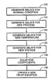
- FIG. 2 illustrates a process for computing the delay of an ASIC cell in accordance with embodiments of the present invention.
- step 100 data points for delays under the nominal condition (Dnom) for a cell are generated.
- the present invention generates the delay data points (Dnom) by conducting SPICE simulation on the cell by using the parameters for the nominal condition (i.e., nominal P, V and T) and the transistor level netlist of the cell.
- the input ramptime (R) and the output load (F) of the cell are varied within a respective range.
- R is varied from Rmin (the minimum value for R) to Rmax (the maximum value for R)
- F is varied from Fmin (the minimum value for F) to Fmax (the maximum value for F) while P, V and T remain unchanged at their nominal values.
- approximately sixty values for Dnom are generated by varying the values of R and F
- Dnom1, Dnom2, Dnom3 and Dnom4 are considered to be most significant in calculating delays for the cell for the purpose of delay derating:
- step 110 the value for P is changed from Pnom to another type of process such as WNWP (weak N and weak P) process or SNSP (strong N or strong P) process while V and T remain unchanged.
- WNWP weak N and weak P
- SNSP strong N or strong P
- a SPICE simulation is conducted with the new P value.
- the R and F are varied as described above.
- the following new delays (Dp1, Dp2, Dp3 and Dp4) are generated with the SPICE simulation:
- step 120 the value for T is changed from Tnom to another temperature value within the operating range of the cell while V and P remain at their nominal values.
- a SPICE simulation is conducted with the new T value.
- the R and F are varied as described above.
- the following new delays (Dt1, Dt2, Dt3 and Dt4) are generated with the SPICE simulation:
- step 130 the value for V is changed from Vnom to another voltage value within the operating range of the cell (e.g., 95% of Vnom or 105% of Vnom) while T and P remain at their nominal values.
- a SPICE simulation is conducted with the new V value.
- the R and F are varied as described above.
- the following new delays (Dv1, Dv2, Dv3 and Dv4) are generated with the SPICE simulation:
- step 140 the following equations are created for the process variation:
- step 150 after solving for m1p, m2p, Ap, Cp, m1t, m2t, At, Ct, m1v, m2v, Av and Cv, the coefficients are applied to the following equation to solve for any new delays for the cell:
- Dnew Dnom +( m 1 p*R+m 2 p*F+Ap*R*F+Cp )+( m 1 v*R+m 2 v*F+Av*R*F+Cv )*( Vnew ⁇ Vnom )+( m 1 t*R+m 2 t*F+At *R*F+Ct )*( Tnew ⁇ Tnom ).
- a new delay can be solved for any given new P, V, T, R and F by using the above equation.
- the value for Dnom may be retrieved from a table which has various values for Dnom at various R and F.
- FIG. 3 is block diagram of a general purpose computer system, representing one of many suitable computer platforms for implementing the methods described above.
- FIG. 3 shows a general purpose computer system 151 in accordance with the present invention.
- computer system 151 includes a central processing unit (CPU) 152 , read-only memory (ROM) 154 , random access memory (RAM) 156 , expansion RAM 158 , input/output (I/O) circuitry 160 , display assembly 162 , input device 164 , and expansion bus 166 .
- Computer system 151 may also optionally include a mass storage unit 168 such as a disk drive unit or nonvolatile memory such as flash memory and a real-time clock 170 .
- CPU 152 is coupled to ROM 154 by a data bus 172 , control bus 174 , and address bus 176 .
- ROM 154 contains the basic operating system for the computer system 151 .
- CPU 152 is also connected to RAM 156 by busses 172 , 174 , and 176 .
- Expansion RAM 158 is optionally coupled to RAM 156 for use by CPU 152 .
- CPU 152 is also coupled to the I/O circuitry 160 by data bus 172 , control bus 174 , and address bus 176 to permit data transfers with peripheral devices.
- I/O circuitry 160 typically includes a number of latches, registers and direct memory access (DMA) controllers. The purpose of I/O circuitry 160 is to provide an interface between CPU 152 and such peripheral devices as display assembly 162 , input device 164 , and mass storage 168 .
- DMA direct memory access
- Display assembly 162 of computer system 151 is an output device coupled to I/O circuitry 160 by a data bus 178 .
- Display assembly 162 receives data from I/O circuitry 160 via bus 178 and displays that data on a suitable screen.
- the screen for display assembly 162 can be a device that uses a cathode-ray tube (CRT), liquid crystal display (LCD), or the like, of the types commercially available from a variety of manufacturers.
- Input device 164 can be a keyboard, a mouse, a stylus working in cooperation with a position-sensing display, or the like.
- the aforementioned input devices are available from a variety of vendors and are well known in the art.
- mass storage 168 is generally considered desirable. However, mass storage 168 can be eliminated by providing a sufficient mount of RAM 156 and expansion RAM 158 to store user application programs and data. In that case, RAMs 156 and 158 can optionally be provided with a backup battery to prevent the loss of data even when computer system 151 is turned off. However, it is generally desirable to have some type of long term mass storage 168 such as a commercially available hard disk drive, nonvolatile memory such as flash memory, battery backed RAM, PC-data cards, or the like.
- a removable storage read/write device 169 may be coupled to I/O circuitry 160 to read from and to write to a removable storage media 171 .
- Removable storage media 171 may represent, for example, a magnetic disk, a magnetic tape, an opto-magnetic disk, an optical disk, or the like. Instructions for implementing the inventive method may be provided, in one embodiment, to a network via such a removable storage media.
- CPU 152 In operation, information is input into the computer system 151 by typing on a keyboard, manipulating a mouse or trackball, or “writing” on a tablet or on position-sensing screen of display assembly 162 .
- CPU 152 then processes the data under control of an operating system and an application program, such as a program to perform steps of the inventive method described above, stored in ROM 154 and/or RAM 116 .
- CPU 152 then typically produces data which is output to the display assembly 162 to produce appropriate images on its screen.
- Expansion bus 166 is coupled to data bus 172 , control bus 174 , and address bus 176 . Expansion bus 166 provides extra ports to couple devices such as network interface circuits, modems, display switches, microphones, speakers, etc. to CPU 152 . Network communication is accomplished through the network interface circuit and an appropriate network.
- Suitable computers for use in implementing the present invention may be obtained from various vendors. Various computers, however, may be used depending upon the size and complexity of the OPC tasks. Suitable computers include mainframe computers, multiprocessor computers, workstations or personal computers. In addition, although a general purpose computer system has been described above, a special-purpose computer may also be used.
- the present invention also relates to machine readable media on which are stored program instructions for performing the methods of this invention.
- Such media includes, by way of example, magnetic disks, magnetic tape, optically readable media such as CD ROMs, semiconductor memory such as PCMCIA cards, etc.
- the medium may take the form of a portable item such as a small disk, diskette, cassette, etc., or it may take the form of a relatively larger or immobile item such as a hard disk drive or RAM provided in a computer.
Abstract
Description
Claims (22)
Priority Applications (1)
| Application Number | Priority Date | Filing Date | Title |
|---|---|---|---|
| US09/515,376 US6820048B1 (en) | 2000-02-29 | 2000-02-29 | 4 point derating scheme for propagation delay and setup/hold time computation |
Applications Claiming Priority (1)
| Application Number | Priority Date | Filing Date | Title |
|---|---|---|---|
| US09/515,376 US6820048B1 (en) | 2000-02-29 | 2000-02-29 | 4 point derating scheme for propagation delay and setup/hold time computation |
Publications (1)
| Publication Number | Publication Date |
|---|---|
| US6820048B1 true US6820048B1 (en) | 2004-11-16 |
Family
ID=33418517
Family Applications (1)
| Application Number | Title | Priority Date | Filing Date |
|---|---|---|---|
| US09/515,376 Expired - Fee Related US6820048B1 (en) | 2000-02-29 | 2000-02-29 | 4 point derating scheme for propagation delay and setup/hold time computation |
Country Status (1)
| Country | Link |
|---|---|
| US (1) | US6820048B1 (en) |
Cited By (11)
| Publication number | Priority date | Publication date | Assignee | Title |
|---|---|---|---|---|
| US20050276135A1 (en) * | 2004-06-10 | 2005-12-15 | Matsushita Electric Industrial Co., Ltd. | Timing analysis method and apparatus |
| US20050289491A1 (en) * | 2004-06-28 | 2005-12-29 | Brad Wright | Method and computer program for estimating cell delay from a table with added voltage swing |
| US20060123369A1 (en) * | 2004-12-03 | 2006-06-08 | Lsi Logic Corporation | Ramptime propagation on designs with cycles |
| US20060190862A1 (en) * | 2005-01-26 | 2006-08-24 | Lee Seuk-Whan | Event driven switch level simulation method and simulator |
| EP1920262A1 (en) * | 2005-08-31 | 2008-05-14 | International Business Machines Corporation | Process and apparatus for estimating circuit delay |
| US20090217226A1 (en) * | 2008-02-26 | 2009-08-27 | Qian Cui | Multiple derating factor sets for delay calculation and library generation in multi-corner STA sign-off flow |
| US20100023904A1 (en) * | 2005-12-09 | 2010-01-28 | Lsi Corporation | Method and Apparatus for Generating Memory Models and Timing Database |
| US20110276933A1 (en) * | 2010-05-06 | 2011-11-10 | International Business Machines Corporation | Method for Supporting Multiple Libraries Characterized at Different Process, Voltage, and Temperature Points |
| US20180137225A1 (en) * | 2016-11-15 | 2018-05-17 | Byungha Joo | Method and system for building a cell library with segmented timing arc delay model |
| US10349172B1 (en) * | 2018-08-08 | 2019-07-09 | Fortemedia, Inc. | Microphone apparatus and method of adjusting directivity thereof |
| US11210444B1 (en) * | 2018-06-22 | 2021-12-28 | Ansys, Inc. | Timing assistant for dynamic voltage drop impact on setup/hold constraints |
Citations (8)
| Publication number | Priority date | Publication date | Assignee | Title |
|---|---|---|---|---|
| US5274568A (en) * | 1990-12-05 | 1993-12-28 | Ncr Corporation | Method of estimating logic cell delay time |
| US5692160A (en) * | 1994-12-14 | 1997-11-25 | Vlsi Technology, Inc. | Temperature, process and voltage variant slew rate based power usage simulation and method |
| US5802349A (en) * | 1996-01-22 | 1998-09-01 | Motorola, Inc. | Method for generating an optimized integrated circuit cell library |
| US5896299A (en) * | 1995-10-13 | 1999-04-20 | Vlsi Technology, Inc. | Method and a system for fixing hold time violations in hierarchical designs |
| US6028995A (en) * | 1998-03-31 | 2000-02-22 | Lsi Logic Corporation | Method of determining delay in logic cell models |
| US6038384A (en) * | 1997-12-12 | 2000-03-14 | Vlsi Technology, Inc. | Input slope timing analysis and non-linear delay table optimization |
| US6090152A (en) * | 1997-03-20 | 2000-07-18 | International Business Machines Corporation | Method and system for using voltage and temperature adders to account for variations in operating conditions during timing simulation |
| US6484297B1 (en) * | 2000-02-29 | 2002-11-19 | Lsi Logic Corporation | 4K derating scheme for propagation delay and setup/hold time computation |
-
2000
- 2000-02-29 US US09/515,376 patent/US6820048B1/en not_active Expired - Fee Related
Patent Citations (8)
| Publication number | Priority date | Publication date | Assignee | Title |
|---|---|---|---|---|
| US5274568A (en) * | 1990-12-05 | 1993-12-28 | Ncr Corporation | Method of estimating logic cell delay time |
| US5692160A (en) * | 1994-12-14 | 1997-11-25 | Vlsi Technology, Inc. | Temperature, process and voltage variant slew rate based power usage simulation and method |
| US5896299A (en) * | 1995-10-13 | 1999-04-20 | Vlsi Technology, Inc. | Method and a system for fixing hold time violations in hierarchical designs |
| US5802349A (en) * | 1996-01-22 | 1998-09-01 | Motorola, Inc. | Method for generating an optimized integrated circuit cell library |
| US6090152A (en) * | 1997-03-20 | 2000-07-18 | International Business Machines Corporation | Method and system for using voltage and temperature adders to account for variations in operating conditions during timing simulation |
| US6038384A (en) * | 1997-12-12 | 2000-03-14 | Vlsi Technology, Inc. | Input slope timing analysis and non-linear delay table optimization |
| US6028995A (en) * | 1998-03-31 | 2000-02-22 | Lsi Logic Corporation | Method of determining delay in logic cell models |
| US6484297B1 (en) * | 2000-02-29 | 2002-11-19 | Lsi Logic Corporation | 4K derating scheme for propagation delay and setup/hold time computation |
Cited By (23)
| Publication number | Priority date | Publication date | Assignee | Title |
|---|---|---|---|---|
| US20050276135A1 (en) * | 2004-06-10 | 2005-12-15 | Matsushita Electric Industrial Co., Ltd. | Timing analysis method and apparatus |
| US7222319B2 (en) * | 2004-06-10 | 2007-05-22 | Matsushita Electric Industrial Co., Ltd. | Timing analysis method and apparatus |
| US7181710B2 (en) * | 2004-06-28 | 2007-02-20 | Lsi Logic Corporation | Device for estimating cell delay from a table with added voltage swing |
| US20050289491A1 (en) * | 2004-06-28 | 2005-12-29 | Brad Wright | Method and computer program for estimating cell delay from a table with added voltage swing |
| US7568175B2 (en) | 2004-12-03 | 2009-07-28 | Lsi Corporation | Ramptime propagation on designs with cycles |
| US20060123369A1 (en) * | 2004-12-03 | 2006-06-08 | Lsi Logic Corporation | Ramptime propagation on designs with cycles |
| US7246336B2 (en) * | 2004-12-03 | 2007-07-17 | Lsi Corporation | Ramptime propagation on designs with cycles |
| US20070234255A1 (en) * | 2004-12-03 | 2007-10-04 | Lsi Logic Corporation | Ramptime propagation on designs with cycles |
| US20060190862A1 (en) * | 2005-01-26 | 2006-08-24 | Lee Seuk-Whan | Event driven switch level simulation method and simulator |
| US7506284B2 (en) * | 2005-01-26 | 2009-03-17 | Samsung Electronics Co., Ltd. | Event driven switch level simulation method and simulator |
| EP1920262A4 (en) * | 2005-08-31 | 2010-11-10 | Ibm | Process and apparatus for estimating circuit delay |
| EP1920262A1 (en) * | 2005-08-31 | 2008-05-14 | International Business Machines Corporation | Process and apparatus for estimating circuit delay |
| US20100023904A1 (en) * | 2005-12-09 | 2010-01-28 | Lsi Corporation | Method and Apparatus for Generating Memory Models and Timing Database |
| US8245168B2 (en) * | 2005-12-09 | 2012-08-14 | Lsi Corporation | Method and apparatus for generating memory models and timing database |
| US20120278775A1 (en) * | 2005-12-09 | 2012-11-01 | Lsi Corporation | Method and Apparatus for Generating Memory Models and Timing Database |
| US8566769B2 (en) * | 2005-12-09 | 2013-10-22 | Lsi Corporation | Method and apparatus for generating memory models and timing database |
| US20090217226A1 (en) * | 2008-02-26 | 2009-08-27 | Qian Cui | Multiple derating factor sets for delay calculation and library generation in multi-corner STA sign-off flow |
| US8539411B2 (en) | 2008-02-26 | 2013-09-17 | Lsi Corporation | Multiple derating factor sets for delay calculation and library generation in multi-corner STA sign-off flow |
| US20110276933A1 (en) * | 2010-05-06 | 2011-11-10 | International Business Machines Corporation | Method for Supporting Multiple Libraries Characterized at Different Process, Voltage, and Temperature Points |
| US8549452B2 (en) * | 2010-05-06 | 2013-10-01 | International Business Machines Corporation | Method for supporting multiple libraries characterized at different process, voltage and temperature points |
| US20180137225A1 (en) * | 2016-11-15 | 2018-05-17 | Byungha Joo | Method and system for building a cell library with segmented timing arc delay model |
| US11210444B1 (en) * | 2018-06-22 | 2021-12-28 | Ansys, Inc. | Timing assistant for dynamic voltage drop impact on setup/hold constraints |
| US10349172B1 (en) * | 2018-08-08 | 2019-07-09 | Fortemedia, Inc. | Microphone apparatus and method of adjusting directivity thereof |
Similar Documents
| Publication | Publication Date | Title |
|---|---|---|
| US6240542B1 (en) | Poly routing for chip interconnects with minimal impact on chip performance | |
| US6714903B1 (en) | Placement and routing of circuits using a combined processing/buffer cell | |
| US10418354B2 (en) | Integrated circuit and computer-implemented method of manufacturing the same | |
| US6675139B1 (en) | Floor plan-based power bus analysis and design tool for integrated circuits | |
| US6415422B1 (en) | Method and system for performing capacitance estimations on an integrated circuit design routed by a global routing tool | |
| US8103996B2 (en) | Method and apparatus for thermal analysis of through-silicon via (TSV) | |
| US5754826A (en) | CAD and simulation system for targeting IC designs to multiple fabrication processes | |
| US6446248B1 (en) | Spare cells placement methodology | |
| US20070094622A1 (en) | Methods, Apparatus and Computer Program Products for Generating Selective Netlists that Include Interconnection Influences at Pre-Layout and Post-Layout Design Stages | |
| US10713410B2 (en) | Method for legalizing mixed-cell height standard cells of IC | |
| US6360350B1 (en) | Method and system for performing circuit analysis on an integrated-circuit design having design data available in different forms | |
| US20200285798A1 (en) | Integrated device and method of forming the same | |
| US6820048B1 (en) | 4 point derating scheme for propagation delay and setup/hold time computation | |
| US6484297B1 (en) | 4K derating scheme for propagation delay and setup/hold time computation | |
| US8539411B2 (en) | Multiple derating factor sets for delay calculation and library generation in multi-corner STA sign-off flow | |
| TW202219807A (en) | System, method and storage medium for capacitance extraction | |
| US6671867B2 (en) | Analytical constraint generation for cut-based global placement | |
| US6327696B1 (en) | Method and apparatus for zero skew routing from a fixed H trunk | |
| US6542834B1 (en) | Capacitance estimation | |
| US6243849B1 (en) | Method and apparatus for netlist filtering and cell placement | |
| TW201935289A (en) | Method for cell swapping | |
| US6519746B1 (en) | Method and apparatus for minimization of net delay by optimal buffer insertion | |
| US11092885B2 (en) | Manufacturing methods of semiconductor devices | |
| US20230267261A1 (en) | Design system, design method and method of manufacture of semiconductor device | |
| JPH09232436A (en) | Method and apparatus for logic synthesis, and method for designing semiconductor integrated circuit |
Legal Events
| Date | Code | Title | Description |
|---|---|---|---|
| AS | Assignment |
Owner name: LSI LOGIC CORPORATION, CALIFORNIA Free format text: ASSIGNMENT OF ASSIGNORS INTEREST;ASSIGNORS:BHUTANI, SANDEEP;VENKATESWARAN, SUBRAMANIAM;REEL/FRAME:010836/0481;SIGNING DATES FROM 20000331 TO 20000404 |
|
| FEPP | Fee payment procedure |
Free format text: PAYOR NUMBER ASSIGNED (ORIGINAL EVENT CODE: ASPN); ENTITY STATUS OF PATENT OWNER: LARGE ENTITY |
|
| FPAY | Fee payment |
Year of fee payment: 4 |
|
| FPAY | Fee payment |
Year of fee payment: 8 |
|
| AS | Assignment |
Owner name: DEUTSCHE BANK AG NEW YORK BRANCH, AS COLLATERAL AG Free format text: PATENT SECURITY AGREEMENT;ASSIGNORS:LSI CORPORATION;AGERE SYSTEMS LLC;REEL/FRAME:032856/0031 Effective date: 20140506 |
|
| AS | Assignment |
Owner name: LSI CORPORATION, CALIFORNIA Free format text: CHANGE OF NAME;ASSIGNOR:LSI LOGIC CORPORATION;REEL/FRAME:033102/0270 Effective date: 20070406 |
|
| AS | Assignment |
Owner name: AVAGO TECHNOLOGIES GENERAL IP (SINGAPORE) PTE. LTD Free format text: ASSIGNMENT OF ASSIGNORS INTEREST;ASSIGNOR:LSI CORPORATION;REEL/FRAME:035390/0388 Effective date: 20140814 |
|
| AS | Assignment |
Owner name: LSI CORPORATION, CALIFORNIA Free format text: TERMINATION AND RELEASE OF SECURITY INTEREST IN PATENT RIGHTS (RELEASES RF 032856-0031);ASSIGNOR:DEUTSCHE BANK AG NEW YORK BRANCH, AS COLLATERAL AGENT;REEL/FRAME:037684/0039 Effective date: 20160201 Owner name: AGERE SYSTEMS LLC, PENNSYLVANIA Free format text: TERMINATION AND RELEASE OF SECURITY INTEREST IN PATENT RIGHTS (RELEASES RF 032856-0031);ASSIGNOR:DEUTSCHE BANK AG NEW YORK BRANCH, AS COLLATERAL AGENT;REEL/FRAME:037684/0039 Effective date: 20160201 |
|
| AS | Assignment |
Owner name: BANK OF AMERICA, N.A., AS COLLATERAL AGENT, NORTH CAROLINA Free format text: PATENT SECURITY AGREEMENT;ASSIGNOR:AVAGO TECHNOLOGIES GENERAL IP (SINGAPORE) PTE. LTD.;REEL/FRAME:037808/0001 Effective date: 20160201 Owner name: BANK OF AMERICA, N.A., AS COLLATERAL AGENT, NORTH Free format text: PATENT SECURITY AGREEMENT;ASSIGNOR:AVAGO TECHNOLOGIES GENERAL IP (SINGAPORE) PTE. LTD.;REEL/FRAME:037808/0001 Effective date: 20160201 |
|
| REMI | Maintenance fee reminder mailed | ||
| LAPS | Lapse for failure to pay maintenance fees | ||
| STCH | Information on status: patent discontinuation |
Free format text: PATENT EXPIRED DUE TO NONPAYMENT OF MAINTENANCE FEES UNDER 37 CFR 1.362 |
|
| FP | Lapsed due to failure to pay maintenance fee |
Effective date: 20161116 |
|
| AS | Assignment |
Owner name: AVAGO TECHNOLOGIES GENERAL IP (SINGAPORE) PTE. LTD., SINGAPORE Free format text: TERMINATION AND RELEASE OF SECURITY INTEREST IN PATENTS;ASSIGNOR:BANK OF AMERICA, N.A., AS COLLATERAL AGENT;REEL/FRAME:041710/0001 Effective date: 20170119 Owner name: AVAGO TECHNOLOGIES GENERAL IP (SINGAPORE) PTE. LTD Free format text: TERMINATION AND RELEASE OF SECURITY INTEREST IN PATENTS;ASSIGNOR:BANK OF AMERICA, N.A., AS COLLATERAL AGENT;REEL/FRAME:041710/0001 Effective date: 20170119 |
|
| AS | Assignment |
Owner name: BELL SEMICONDUCTOR, LLC, ILLINOIS Free format text: ASSIGNMENT OF ASSIGNORS INTEREST;ASSIGNORS:AVAGO TECHNOLOGIES GENERAL IP (SINGAPORE) PTE. LTD.;BROADCOM CORPORATION;REEL/FRAME:044887/0109 Effective date: 20171208 |
|
| AS | Assignment |
Owner name: CORTLAND CAPITAL MARKET SERVICES LLC, AS COLLATERA Free format text: SECURITY INTEREST;ASSIGNORS:HILCO PATENT ACQUISITION 56, LLC;BELL SEMICONDUCTOR, LLC;BELL NORTHERN RESEARCH, LLC;REEL/FRAME:045216/0020 Effective date: 20180124 |
|
| AS | Assignment |
Owner name: BELL NORTHERN RESEARCH, LLC, ILLINOIS Free format text: RELEASE BY SECURED PARTY;ASSIGNOR:CORTLAND CAPITAL MARKET SERVICES LLC;REEL/FRAME:059720/0223 Effective date: 20220401 Owner name: BELL SEMICONDUCTOR, LLC, ILLINOIS Free format text: RELEASE BY SECURED PARTY;ASSIGNOR:CORTLAND CAPITAL MARKET SERVICES LLC;REEL/FRAME:059720/0223 Effective date: 20220401 Owner name: HILCO PATENT ACQUISITION 56, LLC, ILLINOIS Free format text: RELEASE BY SECURED PARTY;ASSIGNOR:CORTLAND CAPITAL MARKET SERVICES LLC;REEL/FRAME:059720/0223 Effective date: 20220401 |