US6771868B2 - Use of deuterated gases for the vapor deposition of thin films for low-loss optical devices and waveguides - Google Patents
Use of deuterated gases for the vapor deposition of thin films for low-loss optical devices and waveguides Download PDFInfo
- Publication number
- US6771868B2 US6771868B2 US10/465,881 US46588103A US6771868B2 US 6771868 B2 US6771868 B2 US 6771868B2 US 46588103 A US46588103 A US 46588103A US 6771868 B2 US6771868 B2 US 6771868B2
- Authority
- US
- United States
- Prior art keywords
- thin film
- deuterium
- vapor deposition
- atomic density
- polymeric
- Prior art date
- Legal status (The legal status is an assumption and is not a legal conclusion. Google has not performed a legal analysis and makes no representation as to the accuracy of the status listed.)
- Expired - Lifetime
Links
Images


Classifications
-
- C—CHEMISTRY; METALLURGY
- C03—GLASS; MINERAL OR SLAG WOOL
- C03C—CHEMICAL COMPOSITION OF GLASSES, GLAZES OR VITREOUS ENAMELS; SURFACE TREATMENT OF GLASS; SURFACE TREATMENT OF FIBRES OR FILAMENTS MADE FROM GLASS, MINERALS OR SLAGS; JOINING GLASS TO GLASS OR OTHER MATERIALS
- C03C4/00—Compositions for glass with special properties
- C03C4/0042—Compositions for glass with special properties for glass comprising or including particular isotopes
-
- C—CHEMISTRY; METALLURGY
- C03—GLASS; MINERAL OR SLAG WOOL
- C03C—CHEMICAL COMPOSITION OF GLASSES, GLAZES OR VITREOUS ENAMELS; SURFACE TREATMENT OF GLASS; SURFACE TREATMENT OF FIBRES OR FILAMENTS MADE FROM GLASS, MINERALS OR SLAGS; JOINING GLASS TO GLASS OR OTHER MATERIALS
- C03C17/00—Surface treatment of glass, not in the form of fibres or filaments, by coating
- C03C17/34—Surface treatment of glass, not in the form of fibres or filaments, by coating with at least two coatings having different compositions
- C03C17/3411—Surface treatment of glass, not in the form of fibres or filaments, by coating with at least two coatings having different compositions with at least two coatings of inorganic materials
- C03C17/3429—Surface treatment of glass, not in the form of fibres or filaments, by coating with at least two coatings having different compositions with at least two coatings of inorganic materials at least one of the coatings being a non-oxide coating
- C03C17/3435—Surface treatment of glass, not in the form of fibres or filaments, by coating with at least two coatings having different compositions with at least two coatings of inorganic materials at least one of the coatings being a non-oxide coating comprising a nitride, oxynitride, boronitride or carbonitride
-
- C—CHEMISTRY; METALLURGY
- C03—GLASS; MINERAL OR SLAG WOOL
- C03C—CHEMICAL COMPOSITION OF GLASSES, GLAZES OR VITREOUS ENAMELS; SURFACE TREATMENT OF GLASS; SURFACE TREATMENT OF FIBRES OR FILAMENTS MADE FROM GLASS, MINERALS OR SLAGS; JOINING GLASS TO GLASS OR OTHER MATERIALS
- C03C17/00—Surface treatment of glass, not in the form of fibres or filaments, by coating
- C03C17/34—Surface treatment of glass, not in the form of fibres or filaments, by coating with at least two coatings having different compositions
- C03C17/3411—Surface treatment of glass, not in the form of fibres or filaments, by coating with at least two coatings having different compositions with at least two coatings of inorganic materials
- C03C17/3429—Surface treatment of glass, not in the form of fibres or filaments, by coating with at least two coatings having different compositions with at least two coatings of inorganic materials at least one of the coatings being a non-oxide coating
- C03C17/3482—Surface treatment of glass, not in the form of fibres or filaments, by coating with at least two coatings having different compositions with at least two coatings of inorganic materials at least one of the coatings being a non-oxide coating comprising silicon, hydrogenated silicon or a silicide
-
- C—CHEMISTRY; METALLURGY
- C23—COATING METALLIC MATERIAL; COATING MATERIAL WITH METALLIC MATERIAL; CHEMICAL SURFACE TREATMENT; DIFFUSION TREATMENT OF METALLIC MATERIAL; COATING BY VACUUM EVAPORATION, BY SPUTTERING, BY ION IMPLANTATION OR BY CHEMICAL VAPOUR DEPOSITION, IN GENERAL; INHIBITING CORROSION OF METALLIC MATERIAL OR INCRUSTATION IN GENERAL
- C23C—COATING METALLIC MATERIAL; COATING MATERIAL WITH METALLIC MATERIAL; SURFACE TREATMENT OF METALLIC MATERIAL BY DIFFUSION INTO THE SURFACE, BY CHEMICAL CONVERSION OR SUBSTITUTION; COATING BY VACUUM EVAPORATION, BY SPUTTERING, BY ION IMPLANTATION OR BY CHEMICAL VAPOUR DEPOSITION, IN GENERAL
- C23C16/00—Chemical coating by decomposition of gaseous compounds, without leaving reaction products of surface material in the coating, i.e. chemical vapour deposition [CVD] processes
- C23C16/22—Chemical coating by decomposition of gaseous compounds, without leaving reaction products of surface material in the coating, i.e. chemical vapour deposition [CVD] processes characterised by the deposition of inorganic material, other than metallic material
- C23C16/30—Deposition of compounds, mixtures or solid solutions, e.g. borides, carbides, nitrides
- C23C16/308—Oxynitrides
-
- C—CHEMISTRY; METALLURGY
- C23—COATING METALLIC MATERIAL; COATING MATERIAL WITH METALLIC MATERIAL; CHEMICAL SURFACE TREATMENT; DIFFUSION TREATMENT OF METALLIC MATERIAL; COATING BY VACUUM EVAPORATION, BY SPUTTERING, BY ION IMPLANTATION OR BY CHEMICAL VAPOUR DEPOSITION, IN GENERAL; INHIBITING CORROSION OF METALLIC MATERIAL OR INCRUSTATION IN GENERAL
- C23C—COATING METALLIC MATERIAL; COATING MATERIAL WITH METALLIC MATERIAL; SURFACE TREATMENT OF METALLIC MATERIAL BY DIFFUSION INTO THE SURFACE, BY CHEMICAL CONVERSION OR SUBSTITUTION; COATING BY VACUUM EVAPORATION, BY SPUTTERING, BY ION IMPLANTATION OR BY CHEMICAL VAPOUR DEPOSITION, IN GENERAL
- C23C16/00—Chemical coating by decomposition of gaseous compounds, without leaving reaction products of surface material in the coating, i.e. chemical vapour deposition [CVD] processes
- C23C16/22—Chemical coating by decomposition of gaseous compounds, without leaving reaction products of surface material in the coating, i.e. chemical vapour deposition [CVD] processes characterised by the deposition of inorganic material, other than metallic material
- C23C16/30—Deposition of compounds, mixtures or solid solutions, e.g. borides, carbides, nitrides
- C23C16/40—Oxides
- C23C16/401—Oxides containing silicon
-
- G—PHYSICS
- G02—OPTICS
- G02B—OPTICAL ELEMENTS, SYSTEMS OR APPARATUS
- G02B6/00—Light guides; Structural details of arrangements comprising light guides and other optical elements, e.g. couplings
- G02B6/10—Light guides; Structural details of arrangements comprising light guides and other optical elements, e.g. couplings of the optical waveguide type
- G02B6/12—Light guides; Structural details of arrangements comprising light guides and other optical elements, e.g. couplings of the optical waveguide type of the integrated circuit kind
- G02B6/13—Integrated optical circuits characterised by the manufacturing method
- G02B6/132—Integrated optical circuits characterised by the manufacturing method by deposition of thin films
-
- C—CHEMISTRY; METALLURGY
- C03—GLASS; MINERAL OR SLAG WOOL
- C03C—CHEMICAL COMPOSITION OF GLASSES, GLAZES OR VITREOUS ENAMELS; SURFACE TREATMENT OF GLASS; SURFACE TREATMENT OF FIBRES OR FILAMENTS MADE FROM GLASS, MINERALS OR SLAGS; JOINING GLASS TO GLASS OR OTHER MATERIALS
- C03C2218/00—Methods for coating glass
- C03C2218/10—Deposition methods
- C03C2218/15—Deposition methods from the vapour phase
- C03C2218/152—Deposition methods from the vapour phase by cvd
-
- C—CHEMISTRY; METALLURGY
- C03—GLASS; MINERAL OR SLAG WOOL
- C03C—CHEMICAL COMPOSITION OF GLASSES, GLAZES OR VITREOUS ENAMELS; SURFACE TREATMENT OF GLASS; SURFACE TREATMENT OF FIBRES OR FILAMENTS MADE FROM GLASS, MINERALS OR SLAGS; JOINING GLASS TO GLASS OR OTHER MATERIALS
- C03C2218/00—Methods for coating glass
- C03C2218/30—Aspects of methods for coating glass not covered above
- C03C2218/32—After-treatment
- C03C2218/328—Partly or completely removing a coating
- C03C2218/33—Partly or completely removing a coating by etching
-
- G—PHYSICS
- G02—OPTICS
- G02B—OPTICAL ELEMENTS, SYSTEMS OR APPARATUS
- G02B6/00—Light guides; Structural details of arrangements comprising light guides and other optical elements, e.g. couplings
- G02B6/10—Light guides; Structural details of arrangements comprising light guides and other optical elements, e.g. couplings of the optical waveguide type
- G02B6/12—Light guides; Structural details of arrangements comprising light guides and other optical elements, e.g. couplings of the optical waveguide type of the integrated circuit kind
- G02B2006/12083—Constructional arrangements
- G02B2006/12097—Ridge, rib or the like
-
- G—PHYSICS
- G02—OPTICS
- G02B—OPTICAL ELEMENTS, SYSTEMS OR APPARATUS
- G02B6/00—Light guides; Structural details of arrangements comprising light guides and other optical elements, e.g. couplings
- G02B6/10—Light guides; Structural details of arrangements comprising light guides and other optical elements, e.g. couplings of the optical waveguide type
- G02B6/12—Light guides; Structural details of arrangements comprising light guides and other optical elements, e.g. couplings of the optical waveguide type of the integrated circuit kind
- G02B2006/12083—Constructional arrangements
- G02B2006/121—Channel; buried or the like
Definitions
- the present invention relates to the vapor deposition of silicon-containing, amorphous thin films, and in particular to vapor deposition of silicon-containing, non-polymeric amorphous thin films with significantly reduced optical absorption (reduced optical loss) in the near-infrared optical communications wavelength region of about 1.45 to 1.65 microns for such uses as in the fabrication of optical devices, such as optical waveguides, ring resonators, arrayed waveguide grating multiplexers/demultiplexers, optical add/drop multiplexers, optical switches, variable attenuators, and dispersion compensators.
- optical devices such as optical waveguides, ring resonators, arrayed waveguide grating multiplexers/demultiplexers, optical add/drop multiplexers, optical switches, variable attenuators, and dispersion compensators.
- silicon-oxide (SiO 2 ) 1 or silicon-oxynitride (SiO x N y ) 2 thin films are grown on a substrate 3 using low pressure chemical vapor deposition (LPCVD) (see, e.g., J. Yota, J. Hander, and A. A. Saleh, “A comparative study on inductively-coupled plasma high-density plasma, plasma-enhanced, and low pressure chemical vapor deposition silicon nitride films,” J. Vac. Sci. Technol.
- LPCVD low pressure chemical vapor deposition
- optical absorption, or loss in the near-infrared optical communication wavelength region from 1.45 to 1.65 microns.
- the absorption occurs at least partially due to an effect commonly referred to as “stretching mode”—the motion of atoms that occurs in perpendicular directions on the same axis, away from each other.
- simple optical waveguides having a waveguide core consisting of vapor deposited SiO x N y show optical losses of 10 dB/cm and higher for optical wavelengths near 1.51 microns, which results from optical absorption by the overtones of the vibrational stretching modes of Si—H and N—H bonds (see, e.g., G. Grand, J. P.
- One way to eliminate this effect is to remove the hydrogen from the substance through which the light is being transmitted.
- a technique commonly used to accomplish this removal is to anneal the films at high temperatures ( ⁇ 1140° C.), driving as much of the hydrogen from the film as possible (see, e.g., R. Germann, H. W. M. Salemink, R. Beyeler, G. L. Bona, F. Horst, I Massarek, and B. J. Offrein, “Silicon oxynitride layers for optical waveguide applications,” Journal of the Electrochemical Society 147 (6), 2237 (2000)).
- This technique can substantially reduce the optical loss in the wavelength region of interest to below 1 dB/cm, but at the expense of an additional process step that can cause shrinkage of the film and introduce significant tensile stress in the film. These effects can create cracks in the film and bowing of the wafers.
- the annealing temperature is high enough to drive hydrogen atoms out of the film, but not high enough to melt the film and allow it to flow and reshape.
- the resulting stretch or bending of the wafer makes the wafer difficult to process using lithography and standard semiconductor processing techniques.
- this process results in a number of dangling bonds of silicon atoms remaining in the film, and if the film is later exposed to sources of hydrogen, such as water vapor from humidity, the hydrogen can react and reattach to the silicon, eventually resulting in the same problem with absorption that was present absent annealing.
- optical devices including non-polymeric passive optical devices and integrated optical devices that have low optical losses at selected wavelengths.
- devices and methods of making devices for use with waveguides on wafers such as planar lightwave circuits, including circuits with multiple devices connected by waveguides on a single wafer, that incorporate other processes than annealing and overcome the problems with this technique.
- the present invention relates to optical devices, including integrated optical devices, and methods for fabrication via vapor deposition of non-polymeric, silicon-containing thin films using vapor sources, such as deuterated liquids, comprised of deuterated species.
- vapor sources such as deuterated liquids, comprised of deuterated species.
- thin films are grown on a substrate to form optical devices or portions thereof that have at least one deuterium containing layer. These devices have significantly reduced optical absorption or loss in the near-infrared optical spectrum, which is the spectrum commonly used for optical communications, compared to the loss in waveguides formed in thin films grown using conventional vapor deposition techniques and hydrogen containing precursors.
- the devices produced in accordance with embodiments of the present invention have deuterium in place of hydrogen within bonds for the formed films.
- Deuterium which is an isotope of hydrogen that has a neutron in its nucleus, vibrates within bonds with other atoms at frequencies different from hydrogen in the same bonds. This difference in frequency results from the increased mass of deuterium over hydrogen. Because of the different frequency of vibration of the deuterium in these bonds, relative to hydrogen, different wavelengths of energy, including light, are absorbed within the materials formed using deuterium than the wavelengths absorbed by the same materials when hydrogen is present.
- Deuterium used in the formation of optical devices in accordance with the present invention results in shifts of energy peaks for these materials, such that the primary band of wavelengths to be transmitted, in the 1.45 to 1.65 micron range, are no longer absorbed by the material of these devices.
- deuterated gases such as SiD 4 and ND 3 (D being deuterium), serving as precursors, along with a gaseous source of oxygen, such as nitrous-oxide (N 2 O) or oxygen (O 2 ), are used for the chemical vapor deposition of silicon-oxynitride (SiO x N y :D) or other non-polymeric thin films on a cladding.
- the cladding is composed, for example, of silicon oxide (SiO 2 ), phosphosilicate glass, fluorinated silicon oxide, or SiO x N y :D having an index of refraction less than that of the thin film.
- the cladding is formed on a substrate, such as silicon, quartz, glass, or other material containing germanium, fused silica, quartz, glass, sapphire, SiC, GaAs, InP, or silicon.
- the thin film and the cladding formed on the substrate can vary in thickness and width, depending, for example, on the device being formed.
- the cladding is formed with a thickness varying from 2 to 20 microns, and the thin film is formed with a thickness varying from about 0.5 to 5 microns. Other thicknesses of the cladding and the thin film are also usable in accordance with the present invention.
- Embodiments of the present invention include formation of the integrated or other optical devices on substrates that include or have formed upon them other electronic or optical devices, or formed portions thereof, referred to herein as “preformed devices.”
- preformed devices can include, for example, field-effect transistors (FETs), such as metal-oxide-semiconductor FETs (MOSFETs), electronic amplifiers, preamplifiers, devices containing pn junctions, transformers, capacitors, diodes, laser drivers, lasers, optical amplifiers, optical detectors, optical waveguides, modulators, optical switches, or other electronic or optical devices.
- FETs field-effect transistors
- MOSFETs metal-oxide-semiconductor FETs
- electronic amplifiers preamplifiers
- devices containing pn junctions transformers, capacitors, diodes
- laser drivers lasers
- optical amplifiers optical detectors
- optical waveguides optical waveguides
- modulators optical switches, or other electronic or optical devices.
- silicon nitride (Si 3 N 4 ) or silicon-oxide (SiO 2 ) films are grown using the techniques of the present invention to eliminate either the oxygen bearing gas or the deuterated ammonia gas, respectively.
- silicon-oxynitride by using deuterated gases instead of the hydrogenated versions of silane and ammonia (SiH 4 and NH 3 ), the resulting thin films have virtually zero hydrogen content and instead contain some deuterium.
- deuterated liquids usable to produce the deuterated gases include deuterated tetraethoxysilane, deuterated tetraethylorthosilicate, deuterated hexamethyldisiloxane, deuterated hexamethyldisilazane, deuterated tetramethoxysilane, and deuterated tetramethyldisiloxane.
- precursors containing deuterium include SiD 4 , Si 2 D 6 , SiDCl 3 , SiCl 2 D 2 , ND 3 , GeD 4 , PD 3 , AsD 3 , CD 4 , and D 2 S.
- Layers may be formed on substrates using deuterated gases, in accordance with embodiments of the present invention, via any of a number of chemical vapor deposition and other techniques known in the art for forming thin layers on integrated components, including plasma enhanced chemical vapor deposition (PECVD), high density plasma chemical vapor deposition (HDPCVD), low pressure chemical vapor deposition (LPCVD), atmospheric pressure chemical vapor deposition (APCVD), jet vapor deposition (JVD), flame hydrolysis, and electron cyclotron resonance (ECR) chemical vapor deposition.
- PECVD plasma enhanced chemical vapor deposition
- HDPCVD high density plasma chemical vapor deposition
- LPCVD low pressure chemical vapor deposition
- APCVD atmospheric pressure chemical vapor deposition
- JVD jet vapor deposition
- ECR electron cyclotron resonance
- Embodiments of the present invention include replacing hydrogen atoms and/or molecules in the source gas species with deuterium in order to virtually eliminate the population of hydrogen in the growth chamber, and the resulting films grown by this method demonstrate complete replacement of incorporated hydrogen with deuterium atoms.
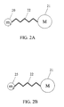
- FIG. 2A is a diagram showing a single bond between two atoms of mass m 1 and M modeled as a simple harmonic oscillator, in accordance with an embodiment of the present invention
- FIG. 2B is a diagram showing a single bond between two atoms of mass m 2 and M modeled as a simple harmonic oscillator, in accordance with an embodiment of the present invention
- FIG. 3A shows a diagram of a 2 ⁇ m thick and 3 ⁇ m wide optical waveguide core formed from a SiO x N y :D film with air and SiO 2 cladding regions and grown on a substrate, such as a silicon substrate, in accordance with an embodiment of the present invention
- FIG. 3B shows a diagram of a 2 ⁇ m thick and 3 ⁇ m wide optical waveguide core formed from a SiO x N y :D film with SiO 2 and other cladding regions and grown on a substrate, such as a silicon substrate, in accordance with an embodiment of the present invention.
- FIG. 4 presents a graph of propagation loss in dB/cm for the waveguide structure shown in FIG. 3, formed from unannealed PECVD grown SiON:D with an index of refraction of 1.59, in accordance with an embodiment of the present invention.
- Embodiments of the present invention include use of one or more deuterated gases or vapors for the chemical vapor deposition of thin, inorganic, glassy films for low-loss near-infrared optical waveguides in the fields of optics and photonics.
- Formed optical layers such as PECVD grown SiO x N y using conventional silane and ammonia, normally contain between 5% and 25% atomic content of hydrogen. This hydrogen exists as Si—H, O—H, and N—H bonds within the film.
- SiO x N y the stretching vibrational modes of Si—H bonds exist in a band around 2200 cm ⁇ 1
- the stretching vibrational modes of N—H bonds exist in a band around 3350 cm ⁇ 1 (see, e.g., J. Yeh and S. C. Lee, “Structural and optical properties of amorphous silcon oxynitride,” J. Appl. Phys. 79 (2), 656 (1996)).
- the resulting mid-infrared absorption data show strong peaks at these energies. More importantly, however, the second overtone of the Si—H vibration and the first overtone of the N—H vibration are in the near-infrared spectral region of interest for optical communication applications, around 1.51 microns.
- the stretching vibrational mode associated with the O—H bond also displays significant absorption around 1.4 micron wavelengths.
- FIG. 2A two atoms 20 , 21 , are linked by bond 22 .
- the first atom 20 represented by a lower case m 1
- the second atom 21 represented by an upper case M
- the first atom 25 is a deuterium atom.
- the vibrational energy associated with the bond 22 can be shown to be as follows:
- ⁇ o ( 1 / 2 ⁇ ⁇ ⁇ ⁇ ⁇ c ) ⁇ ⁇ k ⁇ ( 1 / m + 1 / M ) ( 2 )
- the hydrogen atom consisting of one proton and one electron and having an atomic mass of one
- deuterium consisting of one proton, one neutron, and one electron and having a mass of approximately two times the mass of the hydrogen atom.
- One overall result from applying the methods of the present invention is a much reduced optical absorption loss in these types of waveguides at wavelengths near 1.5 microns, from a value over 10 dB/cm for substances such as SiON:H to below 1 dB/cm for substances such as SiON:D, which is accomplished without the need for an annealing process step as required in the prior art.
- More complex integrated optical devices also benefit greatly when made from deuterium containing glassy films and similarly have a much reduced insertion loss in the spectral range near 1.5 micron wavelengths.
- FIGS. 3A, 3 B, and 4 An example of formation of a device 30 in accordance with the present invention and the results produced will now be described in conjunction with FIGS. 3A, 3 B, and 4 .
- a parallel plate PECVD system was used to deposit a 2 ⁇ m thin film of SiON:D 31 with a nominal index of refraction of 1.59 at a wavelength of 1.55 microns.
- the film is grown on a cladding 33 , such as a 4 ⁇ m thick layer of silicon oxide (SiO 2 ), which is formed on the surface of a substrate 32 , such as a silicon substrate.
- Embodiments of the present invention include formation of the film on a variety of optical cladding materials, and other use of optical cladding with the film of the present invention.
- the optical cladding can include any of a number of materials having a lower index of refraction than the thin film forming the optical component.
- Other example materials include silicon oxide, phosphosilicate glass, fluorinated silicon oxide, and SiO x N y having a lower index of refraction than the SiO x N y :D forming the thin film.
- cladding covers the surface of the thin film 31 .
- This cover cladding in one embodiment, as shown in FIG. 3A is air 35 , which has a lower index of refraction than the thin film 31 .
- the cover cladding 36 is another material, such as the same material as the cladding 33 on the substrate 32 , or alternatively another material having a index of refraction less than that of the thin film 31 , such as a polymer.
- the deposition conditions for the example shown in FIGS. 3A and 3B are as follows: gas flows of 12 sccm N 2 O, 7.2 sccm ND 3 , and 64 sccm of 2% SiD 4 in an N 2 carrier gas with 10 W of 13.5 MHz radiofrequency (RF), a substrate temperature of 300° C., and a chamber pressure of about 300 mTorr.
- the growth rate for this example was approximately 8 nm/min.
- the wafer is processed to create ridge optical waveguides similar in cross-sectional structure to that of the film 31 shown in FIGS. 3A and 3B.
- Another embodiment of the present invention includes formation of the integrated or other optical devices on other electronic or optical devices or formed portions thereof, these preformed devices including, for example, field-effect transistors (FETs), such as metal-oxide-semiconductor FETs (MOSFETs), electronic amplifiers, preamplifiers, devices containing pn junctions, transformers, capacitors, diodes, laser drivers, lasers, optical amplifiers, optical detectors, optical waveguides, modulators, optical switches, or other electronic or optical components.
- FETs field-effect transistors
- MOSFETs metal-oxide-semiconductor FETs
- electronic amplifiers preamplifiers
- devices containing pn junctions transformers, capacitors, diodes, laser drivers, lasers, optical amplifiers, optical detectors, optical waveguides, modulators, optical switches, or other electronic or optical components.
Abstract
Description


Claims (40)
Priority Applications (2)
| Application Number | Priority Date | Filing Date | Title |
|---|---|---|---|
| US10/465,881 US6771868B2 (en) | 2001-07-12 | 2003-06-20 | Use of deuterated gases for the vapor deposition of thin films for low-loss optical devices and waveguides |
| US10/864,511 US7043133B2 (en) | 2001-07-12 | 2004-06-10 | Silicon-oxycarbide high index contrast, low-loss optical waveguides and integrated thermo-optic devices |
Applications Claiming Priority (3)
| Application Number | Priority Date | Filing Date | Title |
|---|---|---|---|
| US30481101P | 2001-07-12 | 2001-07-12 | |
| US09/944,207 US6614977B2 (en) | 2001-07-12 | 2001-09-04 | Use of deuterated gases for the vapor deposition of thin films for low-loss optical devices and waveguides |
| US10/465,881 US6771868B2 (en) | 2001-07-12 | 2003-06-20 | Use of deuterated gases for the vapor deposition of thin films for low-loss optical devices and waveguides |
Related Parent Applications (1)
| Application Number | Title | Priority Date | Filing Date |
|---|---|---|---|
| US09/944,207 Continuation US6614977B2 (en) | 2001-07-12 | 2001-09-04 | Use of deuterated gases for the vapor deposition of thin films for low-loss optical devices and waveguides |
Related Child Applications (1)
| Application Number | Title | Priority Date | Filing Date |
|---|---|---|---|
| US10/864,511 Continuation-In-Part US7043133B2 (en) | 2001-07-12 | 2004-06-10 | Silicon-oxycarbide high index contrast, low-loss optical waveguides and integrated thermo-optic devices |
Publications (2)
| Publication Number | Publication Date |
|---|---|
| US20030210880A1 US20030210880A1 (en) | 2003-11-13 |
| US6771868B2 true US6771868B2 (en) | 2004-08-03 |
Family
ID=26974244
Family Applications (2)
| Application Number | Title | Priority Date | Filing Date |
|---|---|---|---|
| US09/944,207 Expired - Lifetime US6614977B2 (en) | 2001-07-12 | 2001-09-04 | Use of deuterated gases for the vapor deposition of thin films for low-loss optical devices and waveguides |
| US10/465,881 Expired - Lifetime US6771868B2 (en) | 2001-07-12 | 2003-06-20 | Use of deuterated gases for the vapor deposition of thin films for low-loss optical devices and waveguides |
Family Applications Before (1)
| Application Number | Title | Priority Date | Filing Date |
|---|---|---|---|
| US09/944,207 Expired - Lifetime US6614977B2 (en) | 2001-07-12 | 2001-09-04 | Use of deuterated gases for the vapor deposition of thin films for low-loss optical devices and waveguides |
Country Status (4)
| Country | Link |
|---|---|
| US (2) | US6614977B2 (en) |
| EP (1) | EP1425615B1 (en) |
| AU (1) | AU2002322480A1 (en) |
| WO (1) | WO2003007339A2 (en) |
Cited By (4)
| Publication number | Priority date | Publication date | Assignee | Title |
|---|---|---|---|---|
| US20040240820A1 (en) * | 2001-07-12 | 2004-12-02 | Johnson Frederick G. | Silicon-oxycarbide high index contrast, low-loss optical waveguides and integrated thermo-optic devices |
| US20050064729A1 (en) * | 2003-09-23 | 2005-03-24 | Rueger Neal R. | Methods of filling gaps and methods of depositing materials using high density plasma chemical vapor deposition |
| US20070297715A1 (en) * | 2004-08-19 | 2007-12-27 | Infinera Corporation | Integrated optical circuits having drop-in locations for optical circuit elements |
| CN109324369A (en) * | 2018-12-12 | 2019-02-12 | 科新网通科技有限公司 | A kind of production technology of plane waveguiding device |
Families Citing this family (37)
| Publication number | Priority date | Publication date | Assignee | Title |
|---|---|---|---|---|
| US6705124B2 (en) * | 2001-06-04 | 2004-03-16 | Lightwave Microsystems Corporation | High-density plasma deposition process for fabricating a top clad for planar lightwave circuit devices |
| US6614977B2 (en) * | 2001-07-12 | 2003-09-02 | Little Optics, Inc. | Use of deuterated gases for the vapor deposition of thin films for low-loss optical devices and waveguides |
| US6839488B2 (en) * | 2001-09-10 | 2005-01-04 | California Institute Of Technology | Tunable resonant cavity based on the field effect in semiconductors |
| US6990257B2 (en) * | 2001-09-10 | 2006-01-24 | California Institute Of Technology | Electronically biased strip loaded waveguide |
| US7082235B2 (en) * | 2001-09-10 | 2006-07-25 | California Institute Of Technology | Structure and method for coupling light between dissimilar waveguides |
| US20030113085A1 (en) * | 2001-12-14 | 2003-06-19 | Applied Materials, Inc., A Delaware Corporation | HDP-CVD film for uppercladding application in optical waveguides |
| US20030110808A1 (en) * | 2001-12-14 | 2003-06-19 | Applied Materials Inc., A Delaware Corporation | Method of manufacturing an optical core |
| US6730615B2 (en) * | 2002-02-19 | 2004-05-04 | Intel Corporation | High reflector tunable stress coating, such as for a MEMS mirror |
| US6799440B2 (en) * | 2002-02-22 | 2004-10-05 | General Electric Company | Optical fiber deposition tube fused in deuterium atmosphere for attenuation improvement |
| US7010208B1 (en) | 2002-06-24 | 2006-03-07 | Luxtera, Inc. | CMOS process silicon waveguides |
| US6920272B2 (en) * | 2002-10-09 | 2005-07-19 | Nanoopto Corporation | Monolithic tunable lasers and reflectors |
| US7080528B2 (en) * | 2002-10-23 | 2006-07-25 | Applied Materials, Inc. | Method of forming a phosphorus doped optical core using a PECVD process |
| US6943126B1 (en) * | 2002-12-06 | 2005-09-13 | Cypress Semiconductor Corporation | Deuterium incorporated nitride |
| US7723242B2 (en) * | 2004-03-15 | 2010-05-25 | Sharp Laboratories Of America, Inc. | Enhanced thin-film oxidation process |
| KR20060003051A (en) * | 2003-04-23 | 2006-01-09 | 두일전자통신 주식회사 | Method and system for coupling waveguides |
| US7315679B2 (en) * | 2004-06-07 | 2008-01-01 | California Institute Of Technology | Segmented waveguide structures |
| US6865308B1 (en) * | 2004-07-23 | 2005-03-08 | Bae Systems Information And Electronic Systems Integration Inc. | Backside deposition for relieving stress and decreasing warping in optical waveguide production |
| WO2007044554A2 (en) * | 2005-10-07 | 2007-04-19 | Lee, Michael, J. | Amorphous silicon waveguides on iii/v substrates with a barrier layer |
| US7546011B2 (en) * | 2005-10-07 | 2009-06-09 | Novatronix Corporation | Monolithically integrated optical devices with amorphous silicon arrayed waveguide gratings and InGaAsP gain |
| WO2007044514A2 (en) * | 2005-10-07 | 2007-04-19 | Lee, Michael, J. | Method for improving refractive index control in pecvd deposited a-siny films |
| WO2007044543A2 (en) | 2005-10-07 | 2007-04-19 | Lee, Michael, J. | Interface for a-si waveguides and iii/v waveguides |
| US7826688B1 (en) | 2005-10-21 | 2010-11-02 | Luxtera, Inc. | Enhancing the sensitivity of resonant optical modulating and switching devices |
| US20080127313A1 (en) * | 2006-11-29 | 2008-05-29 | Cingular Wireless Ii, Llc | System and method for providing handset insurance in a wireless environment |
| US7526151B1 (en) | 2007-07-16 | 2009-04-28 | Infinera Corporation | Highly symmetric optical structures |
| FR2980394B1 (en) * | 2011-09-26 | 2013-10-18 | Commissariat Energie Atomique | MULTILAYER STRUCTURE PROVIDING IMPROVED GAS SEALING |
| FR2988520B1 (en) * | 2012-03-23 | 2014-03-14 | Arkema France | USE OF A MULTILAYER STRUCTURE BASED ON HALOGEN POLYMER AS A PROTECTIVE SHEET OF PHOTOVOLTAIC MODULE |
| US9018108B2 (en) | 2013-01-25 | 2015-04-28 | Applied Materials, Inc. | Low shrinkage dielectric films |
| JP2016156933A (en) * | 2015-02-24 | 2016-09-01 | 日本電信電話株式会社 | Integrated optical circuit and manufacturing method |
| EP3411740A1 (en) | 2016-02-04 | 2018-12-12 | CommScope Connectivity Belgium BVBA | Integrated optical switches using deuterated liquids for increased bandwidth |
| JP6560153B2 (en) * | 2016-04-12 | 2019-08-14 | 日本電信電話株式会社 | Optical module and manufacturing method thereof |
| JP6930378B2 (en) * | 2017-10-31 | 2021-09-01 | 日本電信電話株式会社 | Semiconductor laser |
| JP6946936B2 (en) * | 2017-10-31 | 2021-10-13 | 日本電信電話株式会社 | Optical waveguide and its manufacturing method |
| JP2019203915A (en) * | 2018-05-21 | 2019-11-28 | 日本電信電話株式会社 | Optical integrated device and method for manufacturing the same |
| JP7071646B2 (en) * | 2019-02-01 | 2022-05-19 | 日本電信電話株式会社 | Tunable laser |
| US11508584B2 (en) | 2019-06-17 | 2022-11-22 | Applied Materials, Inc. | Deuterium-containing films |
| WO2022108986A1 (en) * | 2020-11-17 | 2022-05-27 | Applied Materials, Inc. | An optical device having structural and refractive index gradation, and method of fabricating the same |
| WO2023163994A1 (en) * | 2022-02-23 | 2023-08-31 | PsiQuantum Corp. | Ultra low loss silicon nitride based waveguide |
Citations (39)
| Publication number | Priority date | Publication date | Assignee | Title |
|---|---|---|---|---|
| US4138194A (en) | 1977-10-14 | 1979-02-06 | E. I. Du Pont De Nemours And Company | Low attenuation optical fiber of deuterated polymer |
| US4384038A (en) | 1980-11-25 | 1983-05-17 | U.S. Philips Corporation | Method of producing integrated optical waveguide circuits and circuits obtained by this method |
| USRE31868E (en) | 1977-10-14 | 1985-04-16 | Mitsubishi Rayon Co., Ltd. | Low attenuation optical fiber of deuterated polymer |
| US4583997A (en) | 1983-10-25 | 1986-04-22 | Wacker-Chemitronic Gesellschaft Fur Elektronik Grundstoffe Mbh | Process for reducing the hydroxyl content of optical waveguides |
| US4689065A (en) | 1986-02-14 | 1987-08-25 | American Telephone And Telegraph Company, At&T Bell Laboratories | Optical waveguide glass fiber flame processing |
| US4863236A (en) | 1986-03-06 | 1989-09-05 | Hoechst Aktiengesellschaft | Optical waveguide with an essentially fluorine-free polymer core and a fluorine-containing polymer jacket |
| US5053244A (en) | 1987-02-21 | 1991-10-01 | Leybold Aktiengesellschaft | Process for depositing silicon oxide on a substrate |
| US5059475A (en) | 1990-06-29 | 1991-10-22 | Photonic Integration Research, Inc. | Apparatus and method of forming optical waveguides on metalized substrates |
| US5062680A (en) | 1989-09-27 | 1991-11-05 | Nippon Telegraph And Telephone Corporation | Plate plastics optical waveguide |
| US5175790A (en) | 1989-04-13 | 1992-12-29 | Hoechst Aktiengesellschaft | Transparent thermoplastic molding compound made of 2,3-difluoroacrylic acid esters |
| US5196041A (en) | 1991-09-17 | 1993-03-23 | The Charles Stark Draper Laboratory, Inc. | Method of forming an optical channel waveguide by gettering |
| JPH05173043A (en) * | 1991-11-15 | 1993-07-13 | Fujikura Ltd | Optical fiber array |
| US5295220A (en) | 1991-11-15 | 1994-03-15 | Schott Glaswerke | Process for the production of a thin film optical waveguide of TiO2 |
| US5323482A (en) | 1993-05-27 | 1994-06-21 | General Electric Company | Deuterated organic salts useful in nonlinear optical applications |
| US5385594A (en) | 1991-12-06 | 1995-01-31 | Sumitomo Electric Industries, Ltd. | Method for fabricating an optical waveguide |
| US5503650A (en) | 1992-03-17 | 1996-04-02 | Sumitomo Electric Industries, Ltd. | Method for producing a glass thin film with controlloing an oxide vapor of an additive |
| US5547706A (en) | 1994-07-27 | 1996-08-20 | General Electric Company | Optical thin films and method for their production |
| US5588083A (en) | 1993-09-29 | 1996-12-24 | Akzo Nobel N.V. | Non-linear optically active polycarbonate |
| US5593741A (en) | 1992-11-30 | 1997-01-14 | Nec Corporation | Method and apparatus for forming silicon oxide film by chemical vapor deposition |
| US5672672A (en) | 1994-10-26 | 1997-09-30 | Nippon Telegraph And Telephone Corporation | Polymeric optical mixtures, polymeric optical materials and polymeric optical waveguide |
| US5688896A (en) | 1994-09-26 | 1997-11-18 | Akzo Nobel N.V. | Non-linear optically active polycarbonate |
| US5844363A (en) | 1997-01-23 | 1998-12-01 | The Trustees Of Princeton Univ. | Vacuum deposited, non-polymeric flexible organic light emitting devices |
| US5872387A (en) | 1996-01-16 | 1999-02-16 | The Board Of Trustees Of The University Of Illinois | Deuterium-treated semiconductor devices |
| US5949945A (en) | 1996-02-27 | 1999-09-07 | Hitachi Cable, Ltd. | Optical waveguide, optical module and optical system using the same |
| US5972765A (en) | 1997-07-16 | 1999-10-26 | International Business Machines Corporation | Use of deuterated materials in semiconductor processing |
| US5979188A (en) | 1996-06-22 | 1999-11-09 | Northern Telecom Limited | Method of fabricating a planar waveguide structure |
| US6023093A (en) | 1997-04-28 | 2000-02-08 | Lucent Technologies Inc. | Deuterated direlectric and polysilicon film-based semiconductor devices and method of manufacture thereof |
| US6025280A (en) | 1997-04-28 | 2000-02-15 | Lucent Technologies Inc. | Use of SiD4 for deposition of ultra thin and controllable oxides |
| US6077791A (en) | 1996-12-16 | 2000-06-20 | Motorola Inc. | Method of forming passivation layers using deuterium containing reaction gases |
| US6122934A (en) | 1997-10-22 | 2000-09-26 | Nhk Spring Co., Ltd. | Hot Isostatic pressing of a planar optical waveguide |
| US6144795A (en) | 1996-12-13 | 2000-11-07 | Corning Incorporated | Hybrid organic-inorganic planar optical waveguide device |
| US6154582A (en) | 1995-04-21 | 2000-11-28 | Unisearch Limited | Fabrication method of making silica-based optical devices and opto-electronic devices |
| US6160945A (en) | 1997-09-12 | 2000-12-12 | Samsung Electronics Co., Ltd. | Optical waveguide device for loss absorption and fabrication method thereof |
| US6192712B1 (en) | 1997-03-05 | 2001-02-27 | Nec Corporation | Optical waveguide fabrication method |
| US6211065B1 (en) | 1997-10-10 | 2001-04-03 | Applied Materials, Inc. | Method of depositing and amorphous fluorocarbon film using HDP-CVD |
| US6233381B1 (en) | 1997-07-25 | 2001-05-15 | Corning Incorporated | Photoinduced grating in oxynitride glass |
| WO2001064594A1 (en) | 2000-02-29 | 2001-09-07 | International Business Machines Corporation | MATERIAL FOR SiON-OPTICAL WAVEGUIDES AND METHOD FOR FABRICATING SUCH WAVEGUIDES |
| WO2002035265A2 (en) | 2000-10-20 | 2002-05-02 | Corning Incorporated | Using deuterated source gases to fabricate low loss germanium-doped silicon oxy nitride (gestion-sion) |
| US6614977B2 (en) * | 2001-07-12 | 2003-09-02 | Little Optics, Inc. | Use of deuterated gases for the vapor deposition of thin films for low-loss optical devices and waveguides |
Family Cites Families (2)
| Publication number | Priority date | Publication date | Assignee | Title |
|---|---|---|---|---|
| US6156653A (en) * | 1997-11-03 | 2000-12-05 | Zilog, Inc. | Method of fabricating a MOS device |
| US6768856B2 (en) * | 2001-02-09 | 2004-07-27 | Corning Incorporated | High germanium content waveguide materials |
-
2001
- 2001-09-04 US US09/944,207 patent/US6614977B2/en not_active Expired - Lifetime
-
2002
- 2002-07-12 EP EP02756472.3A patent/EP1425615B1/en not_active Expired - Lifetime
- 2002-07-12 WO PCT/US2002/022283 patent/WO2003007339A2/en not_active Application Discontinuation
- 2002-07-12 AU AU2002322480A patent/AU2002322480A1/en not_active Abandoned
-
2003
- 2003-06-20 US US10/465,881 patent/US6771868B2/en not_active Expired - Lifetime
Patent Citations (40)
| Publication number | Priority date | Publication date | Assignee | Title |
|---|---|---|---|---|
| US4138194A (en) | 1977-10-14 | 1979-02-06 | E. I. Du Pont De Nemours And Company | Low attenuation optical fiber of deuterated polymer |
| USRE31868E (en) | 1977-10-14 | 1985-04-16 | Mitsubishi Rayon Co., Ltd. | Low attenuation optical fiber of deuterated polymer |
| US4384038A (en) | 1980-11-25 | 1983-05-17 | U.S. Philips Corporation | Method of producing integrated optical waveguide circuits and circuits obtained by this method |
| US4583997A (en) | 1983-10-25 | 1986-04-22 | Wacker-Chemitronic Gesellschaft Fur Elektronik Grundstoffe Mbh | Process for reducing the hydroxyl content of optical waveguides |
| US4689065A (en) | 1986-02-14 | 1987-08-25 | American Telephone And Telegraph Company, At&T Bell Laboratories | Optical waveguide glass fiber flame processing |
| US4863236A (en) | 1986-03-06 | 1989-09-05 | Hoechst Aktiengesellschaft | Optical waveguide with an essentially fluorine-free polymer core and a fluorine-containing polymer jacket |
| US5053244A (en) | 1987-02-21 | 1991-10-01 | Leybold Aktiengesellschaft | Process for depositing silicon oxide on a substrate |
| US5175790A (en) | 1989-04-13 | 1992-12-29 | Hoechst Aktiengesellschaft | Transparent thermoplastic molding compound made of 2,3-difluoroacrylic acid esters |
| US5062680A (en) | 1989-09-27 | 1991-11-05 | Nippon Telegraph And Telephone Corporation | Plate plastics optical waveguide |
| US5059475A (en) | 1990-06-29 | 1991-10-22 | Photonic Integration Research, Inc. | Apparatus and method of forming optical waveguides on metalized substrates |
| US5196041A (en) | 1991-09-17 | 1993-03-23 | The Charles Stark Draper Laboratory, Inc. | Method of forming an optical channel waveguide by gettering |
| JPH05173043A (en) * | 1991-11-15 | 1993-07-13 | Fujikura Ltd | Optical fiber array |
| US5295220A (en) | 1991-11-15 | 1994-03-15 | Schott Glaswerke | Process for the production of a thin film optical waveguide of TiO2 |
| US5385594A (en) | 1991-12-06 | 1995-01-31 | Sumitomo Electric Industries, Ltd. | Method for fabricating an optical waveguide |
| US5503650A (en) | 1992-03-17 | 1996-04-02 | Sumitomo Electric Industries, Ltd. | Method for producing a glass thin film with controlloing an oxide vapor of an additive |
| US5593741A (en) | 1992-11-30 | 1997-01-14 | Nec Corporation | Method and apparatus for forming silicon oxide film by chemical vapor deposition |
| US5323482A (en) | 1993-05-27 | 1994-06-21 | General Electric Company | Deuterated organic salts useful in nonlinear optical applications |
| US5332827A (en) | 1993-05-27 | 1994-07-26 | General Electric Company | Deuterated organic salts useful in nonlinear optical applications |
| US5588083A (en) | 1993-09-29 | 1996-12-24 | Akzo Nobel N.V. | Non-linear optically active polycarbonate |
| US5547706A (en) | 1994-07-27 | 1996-08-20 | General Electric Company | Optical thin films and method for their production |
| US5688896A (en) | 1994-09-26 | 1997-11-18 | Akzo Nobel N.V. | Non-linear optically active polycarbonate |
| US5672672A (en) | 1994-10-26 | 1997-09-30 | Nippon Telegraph And Telephone Corporation | Polymeric optical mixtures, polymeric optical materials and polymeric optical waveguide |
| US6154582A (en) | 1995-04-21 | 2000-11-28 | Unisearch Limited | Fabrication method of making silica-based optical devices and opto-electronic devices |
| US5872387A (en) | 1996-01-16 | 1999-02-16 | The Board Of Trustees Of The University Of Illinois | Deuterium-treated semiconductor devices |
| US5949945A (en) | 1996-02-27 | 1999-09-07 | Hitachi Cable, Ltd. | Optical waveguide, optical module and optical system using the same |
| US5979188A (en) | 1996-06-22 | 1999-11-09 | Northern Telecom Limited | Method of fabricating a planar waveguide structure |
| US6144795A (en) | 1996-12-13 | 2000-11-07 | Corning Incorporated | Hybrid organic-inorganic planar optical waveguide device |
| US6077791A (en) | 1996-12-16 | 2000-06-20 | Motorola Inc. | Method of forming passivation layers using deuterium containing reaction gases |
| US5844363A (en) | 1997-01-23 | 1998-12-01 | The Trustees Of Princeton Univ. | Vacuum deposited, non-polymeric flexible organic light emitting devices |
| US6192712B1 (en) | 1997-03-05 | 2001-02-27 | Nec Corporation | Optical waveguide fabrication method |
| US6025280A (en) | 1997-04-28 | 2000-02-15 | Lucent Technologies Inc. | Use of SiD4 for deposition of ultra thin and controllable oxides |
| US6023093A (en) | 1997-04-28 | 2000-02-08 | Lucent Technologies Inc. | Deuterated direlectric and polysilicon film-based semiconductor devices and method of manufacture thereof |
| US5972765A (en) | 1997-07-16 | 1999-10-26 | International Business Machines Corporation | Use of deuterated materials in semiconductor processing |
| US6233381B1 (en) | 1997-07-25 | 2001-05-15 | Corning Incorporated | Photoinduced grating in oxynitride glass |
| US6160945A (en) | 1997-09-12 | 2000-12-12 | Samsung Electronics Co., Ltd. | Optical waveguide device for loss absorption and fabrication method thereof |
| US6211065B1 (en) | 1997-10-10 | 2001-04-03 | Applied Materials, Inc. | Method of depositing and amorphous fluorocarbon film using HDP-CVD |
| US6122934A (en) | 1997-10-22 | 2000-09-26 | Nhk Spring Co., Ltd. | Hot Isostatic pressing of a planar optical waveguide |
| WO2001064594A1 (en) | 2000-02-29 | 2001-09-07 | International Business Machines Corporation | MATERIAL FOR SiON-OPTICAL WAVEGUIDES AND METHOD FOR FABRICATING SUCH WAVEGUIDES |
| WO2002035265A2 (en) | 2000-10-20 | 2002-05-02 | Corning Incorporated | Using deuterated source gases to fabricate low loss germanium-doped silicon oxy nitride (gestion-sion) |
| US6614977B2 (en) * | 2001-07-12 | 2003-09-02 | Little Optics, Inc. | Use of deuterated gases for the vapor deposition of thin films for low-loss optical devices and waveguides |
Non-Patent Citations (9)
| Title |
|---|
| A. Shih, J. Yeh, S. Lee, and T.R. Yang, "Structural and Electronic Differences Between Deuterated and Hydrogenated Amorphous Silicon", J. Appl. Phys. vol. 88, No. 3, pp. 1684-1687, Aug., 1, 2000. |
| Akwani et al, 20020154878 A1, Oct. 2002. |
| G. Grand, J.P. Jadot, H. Denis, S. Valette, A. Fournier, and A.M. Grouillet, "Low-Loss PECVD Silica Chanel Waveguides For Optical Communications", Electronic Letters, vol. 26, No. 25, pp. 2135-2137, Dec. 6<th >1990. |
| G. Grand, J.P. Jadot, H. Denis, S. Valette, A. Fournier, and A.M. Grouillet, "Low-Loss PECVD Silica Chanel Waveguides For Optical Communications", Electronic Letters, vol. 26, No. 25, pp. 2135-2137, Dec. 6th 1990. |
| J. Yeh, and S. Lee, "Structural and Optical Properties of Amorphous Silicon Oxynitride", J. Appl. Phys. vol. 79, No. 2, pp. 656-663, Jan. 15, 1996. |
| J. Yota, J. Hander, and A.A. Saleh, "A Comparative Study on Inductively-Coupled Plasma High-Density Plasma, Plasma-Enhanced, and Low-Pressure Chemical Vapor Deposition Silicon Nitride Films", J. Vac. Sci. Technol. A Vol. 18, No. 2, pp. 372-376, Mar./Apr. 2000. |
| L. Martinu, and D. Poitras, "Plasma Deposition of Optical Films and Coatings: A Review", J. Vac. Sci. Technol. A vol. 18, No. 6, pp. 2619-2645, Nov./Dec. 2000. |
| R. Germann, H.W.M. Salemink, R. Beyeler, G.L.Bona, F. Horst, I. Massarek, and B.J. Offrein, "Silicon Oxynitride Layers for Optical Waveguide Applications", J. Electrochemical Society, vol. 147, No. 6 pp. 2237-2241, 2000. |
| T. Watanabe, N. Ooba, S. Hayashida, T. Kurihara, and S. Imamura, "Polymeric Optical Waveguide Circuits Formed Using Silicone Resin", J. Lightwave Technology, vol. 16, No. 6, pp. 1049-1055, Jun. 1998. |
Cited By (10)
| Publication number | Priority date | Publication date | Assignee | Title |
|---|---|---|---|---|
| US20040240820A1 (en) * | 2001-07-12 | 2004-12-02 | Johnson Frederick G. | Silicon-oxycarbide high index contrast, low-loss optical waveguides and integrated thermo-optic devices |
| US7043133B2 (en) | 2001-07-12 | 2006-05-09 | Little Optics, Inc. | Silicon-oxycarbide high index contrast, low-loss optical waveguides and integrated thermo-optic devices |
| US20050064729A1 (en) * | 2003-09-23 | 2005-03-24 | Rueger Neal R. | Methods of filling gaps and methods of depositing materials using high density plasma chemical vapor deposition |
| US20050196976A1 (en) * | 2003-09-23 | 2005-09-08 | Rueger Neal R. | Methods of filling gaps using high density plasma chemical vapor deposition |
| US7056833B2 (en) | 2003-09-23 | 2006-06-06 | Micron Technology, Inc. | Methods of filling gaps and methods of depositing materials using high density plasma chemical vapor deposition |
| US7202183B2 (en) | 2003-09-23 | 2007-04-10 | Micron Technology, Inc. | Method of filling gaps and methods of depositing materials using high density plasma chemical vapor deposition |
| US7273793B2 (en) | 2003-09-23 | 2007-09-25 | Micron Technology, Inc. | Methods of filling gaps using high density plasma chemical vapor deposition |
| US20070297715A1 (en) * | 2004-08-19 | 2007-12-27 | Infinera Corporation | Integrated optical circuits having drop-in locations for optical circuit elements |
| US7468237B2 (en) | 2004-08-19 | 2008-12-23 | Infinera Corporation | Integrated optical circuits having drop-in locations for optical circuit elements |
| CN109324369A (en) * | 2018-12-12 | 2019-02-12 | 科新网通科技有限公司 | A kind of production technology of plane waveguiding device |
Also Published As
| Publication number | Publication date |
|---|---|
| EP1425615A2 (en) | 2004-06-09 |
| US6614977B2 (en) | 2003-09-02 |
| WO2003007339A2 (en) | 2003-01-23 |
| AU2002322480A1 (en) | 2003-01-29 |
| EP1425615A4 (en) | 2009-09-16 |
| US20030012538A1 (en) | 2003-01-16 |
| US20030210880A1 (en) | 2003-11-13 |
| WO2003007339A3 (en) | 2003-11-06 |
| EP1425615B1 (en) | 2017-03-29 |
Similar Documents
| Publication | Publication Date | Title |
|---|---|---|
| US6771868B2 (en) | Use of deuterated gases for the vapor deposition of thin films for low-loss optical devices and waveguides | |
| US7657143B2 (en) | Method for improving refractive index control in PECVD deposited a-SiNy films | |
| US6449420B1 (en) | Germanium silicon oxynitride high index films for planar waveguides | |
| Gorecki | Optimization of plasma-deposited silicon oxinitride films for optical channel waveguides | |
| Sahu et al. | Influence of hydrogen on losses in silicon oxynitride planar optical waveguides | |
| EP1261554B1 (en) | Method for fabricating SiON-waveguides | |
| DE60211597T2 (en) | PECVD of optical quality silica films | |
| Kim et al. | Influence of hydrogen on SiO2 thick film deposited by PECVD and FHD for silica optical waveguide | |
| US6716476B2 (en) | Method of depositing an optical quality silica film by PECVD | |
| Bazylenko et al. | Fabrication of low-temperature PECVD channel waveguides with significantly improved loss in the 1.50-1.55-μm wavelength range | |
| US6749893B2 (en) | Method of preventing cracking in optical quality silica layers | |
| EP1404892B1 (en) | Manufacture of silica waveguides with minimal absorption | |
| Lee et al. | Ge-doped SiO2 glass films prepared by plasma enhanced chemical vapor deposition for planar waveguides | |
| EP1273677A2 (en) | Method of depositing optical films | |
| Wong et al. | Silicon oxynitride integrated waveguide for on-chip optical interconnects applications | |
| US20030207485A1 (en) | Optical waveguide with layered core and methods of manufacture thereof | |
| Ay | Silicon oxynitride layers for applications in optical waveguides | |
| Wosinski et al. | PECVD technology for low-temperature fabrication of silica-on-silicon-based channel waveguides and devices | |
| Pernas et al. | Silicon oxynitride ECR-PECVD films for integrated optics | |
| Yun et al. | Effects of Annealing Atmosphere on the Characteristics and Optical Properties of SiON Films Prepared Plasma Enhanced Chemical Vapor Deposition | |
| Boswell et al. | Deposition of silicon dioxide films using the helicon diffusion reactor for integrated optics applications | |
| Liu et al. | Simulation and fabrication of amorphous silicon rib-type arrayed waveguide grating | |
| Kim et al. | Asymmetrical single-mode silica waveguide deposited by PECVD |
Legal Events
| Date | Code | Title | Description |
|---|---|---|---|
| STCF | Information on status: patent grant |
Free format text: PATENTED CASE |
|
| AS | Assignment |
Owner name: INFINERA CORPORATION, CALIFORNIA Free format text: ASSIGNMENT OF ASSIGNORS INTEREST;ASSIGNOR:NOMADICS, INC.;REEL/FRAME:018545/0505 Effective date: 20060816 |
|
| AS | Assignment |
Owner name: INFINERA CORPORATION, CALIFORNIA Free format text: ASSIGNMENT OF ASSIGNORS INTEREST;ASSIGNORS:LITTLE OPTICS, INC.;NOMADICS, INC.;REEL/FRAME:018923/0929 Effective date: 20070209 |
|
| FEPP | Fee payment procedure |
Free format text: PAT HOLDER NO LONGER CLAIMS SMALL ENTITY STATUS, ENTITY STATUS SET TO UNDISCOUNTED (ORIGINAL EVENT CODE: STOL); ENTITY STATUS OF PATENT OWNER: LARGE ENTITY |
|
| REFU | Refund |
Free format text: REFUND - SURCHARGE, PETITION TO ACCEPT PYMT AFTER EXP, UNINTENTIONAL (ORIGINAL EVENT CODE: R2551); ENTITY STATUS OF PATENT OWNER: LARGE ENTITY |
|
| FPAY | Fee payment |
Year of fee payment: 4 |
|
| SULP | Surcharge for late payment | ||
| FPAY | Fee payment |
Year of fee payment: 8 |
|
| FPAY | Fee payment |
Year of fee payment: 12 |