US6643151B1 - Multiple output dynamically regulated charge pump power converter - Google Patents

Multiple output dynamically regulated charge pump power converter Download PDF

Info

Publication number
US6643151B1
US6643151B1 US09/652,849 US65284901A US6643151B1 US 6643151 B1 US6643151 B1 US 6643151B1 US 65284901 A US65284901 A US 65284901A US 6643151 B1 US6643151 B1 US 6643151B1
Authority
US
United States
Prior art keywords
voltage
power
capacitor
power converter
output
Prior art date
Legal status (The legal status is an assumption and is not a legal conclusion. Google has not performed a legal analysis and makes no representation as to the accuracy of the status listed.)
Expired - Fee Related, expires
Application number
US09/652,849
Inventor
Dragan Danilo Nebrigic
Milan Marcel Jevtitch
Vladimir Gartstein
William Thomas Milam
James Vig Sherrill
Nicholas Busko
Peter Hansen
Current Assignee (The listed assignees may be inaccurate. Google has not performed a legal analysis and makes no representation or warranty as to the accuracy of the list.)
University of Illinois
Nokia of America Corp
Original Assignee
University of Illinois
Priority date (The priority date is an assumption and is not a legal conclusion. Google has not performed a legal analysis and makes no representation as to the accuracy of the date listed.)
Filing date
Publication date
Assigned to LUCENT TECHNOLOGIES INC. reassignment LUCENT TECHNOLOGIES INC. ASSIGNMENT OF ASSIGNORS INTEREST (SEE DOCUMENT FOR DETAILS). Assignors: KUMAR, SARATH, MONOGIOUDIS, PANTELIS, REGE, KIRAN M., SAMPATH, ASHWIN
Assigned to PROCTER & GAMBLE COMPANY, THE reassignment PROCTER & GAMBLE COMPANY, THE ASSIGNMENT OF ASSIGNORS INTEREST (SEE DOCUMENT FOR DETAILS). Assignors: BUSKO, NICHOLAS, GARTSTEIN, VLADMIR, HANSEN, PETER, JEVTITCH, MILAN MARCEI, MILAM, WILLIAM THOMAS, NEBRIGIC, DRAGAN DANILO, SHERRILL, JAMES VIG
Application filed by University of Illinois filed Critical University of Illinois
Priority to US09/652,849 priority Critical patent/US6643151B1/en
Assigned to BOARD OF TRUSTEES OF THE UNIVERSITY OF ILLINOIS, THE reassignment BOARD OF TRUSTEES OF THE UNIVERSITY OF ILLINOIS, THE ASSIGNMENT OF ASSIGNORS INTEREST (SEE DOCUMENT FOR DETAILS). Assignors: PROCTER & GAMBLE COMPANY, THE
Application granted granted Critical
Publication of US6643151B1 publication Critical patent/US6643151B1/en
Adjusted expiration legal-status Critical
Expired - Fee Related legal-status Critical Current

Links

Images

Classifications

    • HELECTRICITY
    • H02GENERATION; CONVERSION OR DISTRIBUTION OF ELECTRIC POWER
    • H02JCIRCUIT ARRANGEMENTS OR SYSTEMS FOR SUPPLYING OR DISTRIBUTING ELECTRIC POWER; SYSTEMS FOR STORING ELECTRIC ENERGY
    • H02J7/00Circuit arrangements for charging or depolarising batteries or for supplying loads from batteries
    • HELECTRICITY
    • H01ELECTRIC ELEMENTS
    • H01MPROCESSES OR MEANS, e.g. BATTERIES, FOR THE DIRECT CONVERSION OF CHEMICAL ENERGY INTO ELECTRICAL ENERGY
    • H01M6/00Primary cells; Manufacture thereof
    • H01M6/50Methods or arrangements for servicing or maintenance, e.g. for maintaining operating temperature
    • H01M6/5044Cells or batteries structurally combined with cell condition indicating means
    • HELECTRICITY
    • H01ELECTRIC ELEMENTS
    • H01MPROCESSES OR MEANS, e.g. BATTERIES, FOR THE DIRECT CONVERSION OF CHEMICAL ENERGY INTO ELECTRICAL ENERGY
    • H01M10/00Secondary cells; Manufacture thereof
    • H01M10/42Methods or arrangements for servicing or maintenance of secondary cells or secondary half-cells
    • H01M10/48Accumulators combined with arrangements for measuring, testing or indicating the condition of cells, e.g. the level or density of the electrolyte
    • H01M10/488Cells or batteries combined with indicating means for external visualization of the condition, e.g. by change of colour or of light density
    • HELECTRICITY
    • H02GENERATION; CONVERSION OR DISTRIBUTION OF ELECTRIC POWER
    • H02MAPPARATUS FOR CONVERSION BETWEEN AC AND AC, BETWEEN AC AND DC, OR BETWEEN DC AND DC, AND FOR USE WITH MAINS OR SIMILAR POWER SUPPLY SYSTEMS; CONVERSION OF DC OR AC INPUT POWER INTO SURGE OUTPUT POWER; CONTROL OR REGULATION THEREOF
    • H02M3/00Conversion of dc power input into dc power output
    • H02M3/02Conversion of dc power input into dc power output without intermediate conversion into ac
    • H02M3/04Conversion of dc power input into dc power output without intermediate conversion into ac by static converters
    • H02M3/06Conversion of dc power input into dc power output without intermediate conversion into ac by static converters using resistors or capacitors, e.g. potential divider
    • H02M3/07Conversion of dc power input into dc power output without intermediate conversion into ac by static converters using resistors or capacitors, e.g. potential divider using capacitors charged and discharged alternately by semiconductor devices with control electrode, e.g. charge pumps
    • HELECTRICITY
    • H02GENERATION; CONVERSION OR DISTRIBUTION OF ELECTRIC POWER
    • H02MAPPARATUS FOR CONVERSION BETWEEN AC AND AC, BETWEEN AC AND DC, OR BETWEEN DC AND DC, AND FOR USE WITH MAINS OR SIMILAR POWER SUPPLY SYSTEMS; CONVERSION OF DC OR AC INPUT POWER INTO SURGE OUTPUT POWER; CONTROL OR REGULATION THEREOF
    • H02M3/00Conversion of dc power input into dc power output
    • H02M3/02Conversion of dc power input into dc power output without intermediate conversion into ac
    • H02M3/04Conversion of dc power input into dc power output without intermediate conversion into ac by static converters
    • H02M3/10Conversion of dc power input into dc power output without intermediate conversion into ac by static converters using discharge tubes with control electrode or semiconductor devices with control electrode
    • H02M3/145Conversion of dc power input into dc power output without intermediate conversion into ac by static converters using discharge tubes with control electrode or semiconductor devices with control electrode using devices of a triode or transistor type requiring continuous application of a control signal
    • H02M3/155Conversion of dc power input into dc power output without intermediate conversion into ac by static converters using discharge tubes with control electrode or semiconductor devices with control electrode using devices of a triode or transistor type requiring continuous application of a control signal using semiconductor devices only
    • H02M3/156Conversion of dc power input into dc power output without intermediate conversion into ac by static converters using discharge tubes with control electrode or semiconductor devices with control electrode using devices of a triode or transistor type requiring continuous application of a control signal using semiconductor devices only with automatic control of output voltage or current, e.g. switching regulators
    • H02M3/158Conversion of dc power input into dc power output without intermediate conversion into ac by static converters using discharge tubes with control electrode or semiconductor devices with control electrode using devices of a triode or transistor type requiring continuous application of a control signal using semiconductor devices only with automatic control of output voltage or current, e.g. switching regulators including plural semiconductor devices as final control devices for a single load
    • H02M3/1588Conversion of dc power input into dc power output without intermediate conversion into ac by static converters using discharge tubes with control electrode or semiconductor devices with control electrode using devices of a triode or transistor type requiring continuous application of a control signal using semiconductor devices only with automatic control of output voltage or current, e.g. switching regulators including plural semiconductor devices as final control devices for a single load comprising at least one synchronous rectifier element
    • HELECTRICITY
    • H02GENERATION; CONVERSION OR DISTRIBUTION OF ELECTRIC POWER
    • H02JCIRCUIT ARRANGEMENTS OR SYSTEMS FOR SUPPLYING OR DISTRIBUTING ELECTRIC POWER; SYSTEMS FOR STORING ELECTRIC ENERGY
    • H02J2207/00Indexing scheme relating to details of circuit arrangements for charging or depolarising batteries or for supplying loads from batteries
    • H02J2207/20Charging or discharging characterised by the power electronics converter
    • YGENERAL TAGGING OF NEW TECHNOLOGICAL DEVELOPMENTS; GENERAL TAGGING OF CROSS-SECTIONAL TECHNOLOGIES SPANNING OVER SEVERAL SECTIONS OF THE IPC; TECHNICAL SUBJECTS COVERED BY FORMER USPC CROSS-REFERENCE ART COLLECTIONS [XRACs] AND DIGESTS
    • Y02TECHNOLOGIES OR APPLICATIONS FOR MITIGATION OR ADAPTATION AGAINST CLIMATE CHANGE
    • Y02BCLIMATE CHANGE MITIGATION TECHNOLOGIES RELATED TO BUILDINGS, e.g. HOUSING, HOUSE APPLIANCES OR RELATED END-USER APPLICATIONS
    • Y02B40/00Technologies aiming at improving the efficiency of home appliances, e.g. induction cooking or efficient technologies for refrigerators, freezers or dish washers
    • YGENERAL TAGGING OF NEW TECHNOLOGICAL DEVELOPMENTS; GENERAL TAGGING OF CROSS-SECTIONAL TECHNOLOGIES SPANNING OVER SEVERAL SECTIONS OF THE IPC; TECHNICAL SUBJECTS COVERED BY FORMER USPC CROSS-REFERENCE ART COLLECTIONS [XRACs] AND DIGESTS
    • Y02TECHNOLOGIES OR APPLICATIONS FOR MITIGATION OR ADAPTATION AGAINST CLIMATE CHANGE
    • Y02BCLIMATE CHANGE MITIGATION TECHNOLOGIES RELATED TO BUILDINGS, e.g. HOUSING, HOUSE APPLIANCES OR RELATED END-USER APPLICATIONS
    • Y02B70/00Technologies for an efficient end-user side electric power management and consumption
    • Y02B70/10Technologies improving the efficiency by using switched-mode power supplies [SMPS], i.e. efficient power electronics conversion e.g. power factor correction or reduction of losses in power supplies or efficient standby modes
    • YGENERAL TAGGING OF NEW TECHNOLOGICAL DEVELOPMENTS; GENERAL TAGGING OF CROSS-SECTIONAL TECHNOLOGIES SPANNING OVER SEVERAL SECTIONS OF THE IPC; TECHNICAL SUBJECTS COVERED BY FORMER USPC CROSS-REFERENCE ART COLLECTIONS [XRACs] AND DIGESTS
    • Y02TECHNOLOGIES OR APPLICATIONS FOR MITIGATION OR ADAPTATION AGAINST CLIMATE CHANGE
    • Y02EREDUCTION OF GREENHOUSE GAS [GHG] EMISSIONS, RELATED TO ENERGY GENERATION, TRANSMISSION OR DISTRIBUTION
    • Y02E60/00Enabling technologies; Technologies with a potential or indirect contribution to GHG emissions mitigation
    • Y02E60/10Energy storage using batteries

Definitions

  • the present invention relates to DC/DC power supply controllers, and more particularly to regulated charge pump power converters for integrated power management systems.
  • portable electronic devices Advances in electronics technology have enabled the design and cost-effective fabrication of portable electronic devices. Thus, usage of portable electronic devices continues to increase both in the number of products available and the types of products. Examples of the broad spectrum of portable electronic devices include pagers, cellular telephones, music players, calculators, laptop computers, and personal digital assistants, as well as others.
  • the electronics in a portable electronic device generally require direct current (DC) electrical power.
  • DC direct current
  • one or more batteries are used as an energy source to provide this DC electrical power.
  • the energy source would be perfectly matched to the energy requirements of the portable electronic device.
  • the voltage and current from the batteries is unsuitable for directly powering the electronics of the portable electronic device.
  • the voltage level from the batteries may differ from the voltage level required by the device.
  • some portions of the electronics may operate at a different voltage level than other portions, requiring different energy source voltage levels.
  • batteries are unable to respond quickly to rapid fluctuations in current demand.
  • FIG. 1 The typical arrangement is shown in FIG. 1 for a portable electronic device 10 that includes an energy source 12 , such as the one or more batteries, and a load device 14 , such as the electronics that require electrical power. Interposed between the energy source 12 and the load device 14 is a power supply 16 that may perform a number of functions.
  • a power converter 20 depicted as integral to the power supply 16 , provides the necessary changes to the power from the energy source 12 to make it suitable for load device 14 .
  • the power supply 16 may also perform functions other than power conversion. For example, protecting the energy source 12 , load device 14 and/or power converter 20 from damage by a sustained high electrical current may require electrically disconnecting the energy source 12 from the rest of the portable electronic device 10 . As another example, the power converter 20 may require assistance during start-up.
  • the power converter 20 may “step up” (i.e., boost) or “step down” the voltage. That is, the converter 20 may increase or decrease the output voltage V OUT provided to the load device 14 with respect to the input voltage Vs from the energy source 12 .
  • the power converter 20 may also store an amount of energy to satisfy a brief spike or increase in demand by the load device 14 that the energy source 12 is unable to provide.
  • the power converter 20 may also regulate the output voltage V OUT , keeping it close to the desired output voltage level and reducing rapid fluctuations that may cause detrimental noise or cause undesirable performance of the load device 14 . Such fluctuations may occur due to changes in demand, induced noise from external electromagnetic sources, characteristics of the energy source 12 , and/or noise from other components in the power supply 16 .
  • power converters 20 provide many benefits, existing power converters 20 also place undesirable performance constraints on portable electronic devices 10 .
  • the specific attributes of generally known power converters 20 are discussed below along with the types of constraints generally encountered.
  • Many generally known power converters 20 are optimized for a specific energy source 12 and a specific load demand from the load device 14 .
  • the power converter 20 may not accommodate, or only accommodate inefficiently, variations in the voltage and current characteristics of the energy source 12 and/or the load device 14 .
  • some types of power converters 20 cannot provide an output voltage V OUT that is higher than the input voltage V S and/or their efficiency is related to how close the input voltage V S is to the required output voltage V OUT .
  • some power converters 20 are incapable of providing medium power levels such as 0.5-1.0 W.
  • generally known power converters 20 have a design that will only operate within a narrow range of input voltages, output voltages and power capacities.
  • some power converters 20 achieve an acceptably regulated output voltage V OUT only through inefficient voltage regulators.
  • voltage regulation by the power converter 20 is inadequate for the needs of the load device 14 .
  • the nominal output voltage V OUT may vary due to variations in the input voltage V S , variations in the temperature of the power converter or the output current drawn by the load device 14 .
  • the power converter 20 may undesirably oscillate about the nominal output voltage V OUT .
  • This voltage ripple V RIP is defined as the range of the oscillations about the nominal output voltage V OUT and may impair or preclude proper operation of the load device 14 .
  • existing power converters 20 do not efficiently provide on demand the required power to a load device, nor adjust to variations in the energy source and load device to provide a stable V OUT .
  • existing power converters 20 do not operate with low input voltage levels, such as a sub-one volt input voltage V S .
  • the existing power converters 20 usually require an operational bias voltage that is typically comparable to the output voltage demands of the load device 14 , which are generally greater than one volt.
  • a certain amount of noise is superimposed on the input voltage V S by external and internal sources. When the input voltage level V S is low, this noise may become relatively significant, degrading or precluding operation of the power converter 20 .
  • an otherwise desirable single cell battery, or an alternative source of power may be inappropriate as an energy source 12 for the device 10 .
  • the nominal voltage supplied by certain electrochemical batteries or alternative sources of power may be below one volt, or have a voltage characteristic that decreases as their stored charge decreases.
  • Such batteries have a significant amount, and perhaps a majority of, their stored energy, which is retrievable only at a sub-one volt level. Consequently, the service life of the battery in a portable electronic device 10 is limited by the inability of the device to operate with a sub-one volt input voltage V S from the battery. As a result, batteries are discarded with a significant amount of charge or “life” still left in them. Achieving additional service life by incorporating additional batteries into the device 10 increases the size and weight of the device 10 .
  • a power converter 20 can continuously operate at a sub-one volt input voltage V S , generally a higher input voltage level (i.e. over 1 volt) is required to start the power converter 20 . That is, the converter requires a higher input voltage at the start-up phase than is necessary for continuous operation (e.g., 0.4 V higher). Therefore, the power converter 20 must be continuously operated once the minimum start-up input voltage is reached, thus consuming power, in order to enhance the amount of energy that is retrieved from the energy source 12 .
  • an external start-up circuit (such as a Schottky diode) is often added to the existing power converters 20 .
  • the start-up circuit assists in overcoming the additional input voltage requirement at start-up and in shortening the period of time required for the power converter 20 to reach its designed output voltage.
  • generally known start-up circuits are usually not capable of operating at sub-one volt input voltage.
  • having to use an external start-up circuit limits the ability to miniaturize the power converter 20 .
  • external start-up circuits tend to dissipate power even when the power converter 20 is not in a start-up condition, thereby reducing the efficiency of the power converter 20 .
  • existing power converters 20 are generally incapable of starting with a sub-one volt input voltage, nor efficiently provide for start-up with a greater than one volt input voltage.
  • CMOS Complementary Metal Oxide Semiconductor
  • each feature may act as a Radio Frequency (RF) antenna, emitting Electromagnetic Interference (EMI) to adjacent features.
  • RF Radio Frequency
  • EMI Electromagnetic Interference
  • the heat generated by the features is typically proportional to the operating frequency; however, the heat generated is also quadratically related to the operating voltage, that is, reducing the operating voltage by half reduces the heat generated to a quarter.
  • the resultant trend in lower operating voltage can be seen by typical microprocessors using 5 V in 1990, 3.3 V in 1995, 1.8-2.4 V in 1998, 1.2-2.4 V in 2000, and 1 V or less expected thereafter.
  • the distance between features is reduced, and thus the amount of insulating material between the features is reduced. Consequently, a lower operating voltage avoids a breakdown through the thinner insulating material between features that would cause microprocessor failure.
  • Still another drawback to existing power converters 20 is that they are not suitable for the desired level of miniaturization in portable devices and are not appropriate for embedded applications, even considering integrated circuit structures such as Silicon On Insulator (SOI) and Silicon On Metal (SOM).
  • SOI Silicon On Insulator
  • SOM Silicon On Metal
  • miniaturization is not possible due to the number of discrete external components necessary that are not amenable to integrated circuit fabrication. These components thus require a printed circuit board (PCB), hybrid or multi-chip module (MCM) design wherein the size and expense of such fabrication is higher than for an entirely integrated circuit.
  • PCB printed circuit board
  • MCM multi-chip module
  • EMI electromagnetic interference
  • the EMI may be from an inductor incorporated into the power converter 20 , or the result of reducing the feature size of the circuits in the power converter 20 .
  • the energy storage and transfer capability is necessarily also reduced. Therefore, a higher operating frequency is required to transfer an equivalent amount of power.
  • the higher operating frequency also results in EMI that is detrimental to the portable electronic device 10 .
  • the portable electronic device 10 itself generally has federally mandated limits on RF emissions that may be exceeded by a sufficiently high operating frequency.
  • the power converter 20 should advantageously generate minimal amounts of heat or radiated energy (EMI) to the load device 14 , and thus be suitable for being embedded on the same integrated circuit or module.
  • EMI radiated energy
  • portable wireless telecommunication devices include processing, memory, transmission, and display functions that by necessity operate at different voltages. Many of these elements require voltage regulation and low EMI in order to perform satisfactorily. Moreover, it is typically desirable to extend battery life and to provide for small device size.
  • the invention overcomes the above-noted and other deficiencies of the prior art by providing an apparatus and method for a dynamically controlled, intrinsically regulated power converter that efficiently transfers power from an energy source as demanded by a load device.
  • a dynamic controller operates a capacitive power output stage to pump charge at a rate to maintain an output voltage V OUT across a load capacitor C L . More particularly, the dynamic controller discharges a fly capacitor C F into the load capacitor C L when the output voltage V OUT drops below a reference voltage V REF . Therefore, operating at a level corresponding to the demand of the load enhances the efficiency of the power converter. Furthermore, the output voltage V OUT is intrinsically regulated in that charge is transferred at a rate to maintain a predetermined voltage level. Therefore, an inefficient downstream voltage regulator is not needed.
  • a power converter is operable with a sub-one volt input voltage V S by advantageously incorporating low control threshold switches in the dynamic controller and the capacitive power output stage.
  • a power converter is operable with a sub-one volt input voltage from a discharged condition by utilizing a progressive startup switch that charges a startup capacitor when the dynamic controller is off. Once charged, the startup capacitor in turn closes a power is switch in the output stage to provide charge to the load capacitor C L until the load capacitor C L is sufficiently charged for the dynamic controller to assume control of the power output stage.
  • a power converter provides a predetermined output voltage, either increased or decreased (stepped up or down) with respect to the input voltage.
  • the power converter may flexibly provide an output voltage with intrinsic regulation insensitive to factors such as the input voltage and temperature so that a predetermined low output voltages, for example 0.8-1.6 V or lower, are efficiently provided.
  • an integrated power converter provides efficient and regulated power conversation, and thus generates little heat.
  • the integrated power converter has inherently low EMI emission by being capacitance only, without an inductor.
  • the integrated power converter mitigates EMI emissions during low capacity demand by switching more slowly.
  • the lack of an inductor enables some applications to be further miniaturized by having no external components by incorporating integrated circuit capacitors.
  • the integrated power converter may advantageously be embedded in an integrated circuit with a load device.
  • the integrated power converter is adapted for low input and/or low output voltage.
  • FIG. 1 is a top-level block diagram of a portable electronic device incorporating a power supply with a power converter.
  • FIG. 2 is a top-level block diagram of an oscillator-controlled power converter (open-loop charge pump).
  • FIG. 3 is a top-level block diagram of a dynamically controlled, intrinsically regulated power converter.
  • FIG. 4 is one embodiment of a circuit for a power output stage for the power converter of FIG. 3 .
  • FIG. 5 is another embodiment of a circuit for a power output stage for the power converter of FIG. 3 .
  • FIG. 6 is a voltage plot of boundary conditions for the maximum load condition for the power output stage of FIG. 5 .
  • FIG. 7 is a top-level block diagram of an embodiment of a dynamically controlled power converter.
  • FIG. 8 is a flow diagram for the operation of the power converter of FIG. 7 .
  • FIG. 9 is a flow diagram for the start-up operation of FIG. 8 .
  • FIG. 10 is a flow diagram for the dynamic operation of FIG. 8 .
  • FIG. 11 is an embodiment of a circuit for a power output stage for the power converter of FIG. 7 .
  • FIG. 12 is an embodiment of a power controller circuit for the power converter of FIG. 7 .
  • FIG. 13 is an embodiment of a voltage reference circuit for the power controller of FIG. 12 .
  • FIG. 14 is an embodiment of a comparator circuit for the power controller of FIG. 12 .
  • FIG. 15 is a more detailed circuit for the comparator circuit of FIG. 14 .
  • FIG. 16 is an embodiment of a timing controller circuit for the power controller of FIG. 12 .
  • FIG. 17 is an illustrative timing diagram for the timing control circuit of FIG. 16 .
  • FIG. 18 is an embodiment of a multiple-output power converter integrated circuit component including integral capacitive elements.
  • FIG. 19 is a block diagram of the multi-output power converter of FIG. 18 .
  • FIG. 20 is an embodiment of one of the power output stages of the multi-output power converter of FIG. 19 .
  • FIG. 21 is an embodiment of an output controller of the multi-output controller of FIG. 19 .
  • FIG. 22 is a circuit diagram for the output controller of FIG. 22 .
  • FIG. 23 is a circuit for the power up signal referenced in FIG. 22 .
  • FIG. 24 is a pin-out diagram for the multi-output power converter of FIGS. 19-23.
  • a linear regulator is one type of existing power converter.
  • Linear regulators have an efficiency that is directly proportional to the ratio of the input voltage V S to the output voltage V OUT .
  • an input voltage V S that is twice the required output voltage V OUT would result in about half of the power from an energy source 12 being inefficiently consumed by the power converter 20 .
  • Due to the lower efficiency and resulting heat generation, linear regulators require a heat sink that often complicates or precludes integration into low profile packages such as those complying with the PCMCIA specification standard.
  • linear regulators generally require two discrete capacitors, further limiting reductions in size.
  • linear regulators cannot step-up the input voltage V S and thus are inappropriate for certain applications.
  • a small portable electronic device 10 such as a hearing aid may benefit from an inexpensive, single-cell alkaline battery that provides a voltage of 0.8-1.4 V.
  • the load device 14 in this case the electronics of the hearing aid, may require 3.0 V. Linear regulators are unsuitable for such an application.
  • Inductor-based power converters and capacitance-only (“charge pump”) power converters are each capable of stepping up or stepping down an input voltage V S .
  • Such designs generally require 1.5-3.3 V input voltage V S and provide an output voltage V OUT from 1.8-5.0 V, with the delivered current between 10-200 mA continuous.
  • sub-one volt input voltages or output voltages are generally not possible.
  • output power in the 200-500 mW range are also generally not available, except through approaches such as placing multiple power converters 20 in parallel to combine their respective outputs, and thus the power consumed by the combination increases.
  • Inductor-based power converters are typically chosen over capacitance-only charge pump power converters for low power applications (e.g., up to 200 mW) since they are relatively efficient compared to a charge pump design. Also, the desired output voltage V OUT is easier to achieve than with charge pumps. Specifically, the output voltage V OUT is proportional to the inductance value of the inductor multiplied by the derivative of the electrical current (di/dt). Consequently, higher operating frequency and/or higher electrical current levels at the input generally do not directly affect the achieved output voltage.
  • inductor-based power converters generally require a non-linear ferrite coil or ferrite bead for the inductor, and also require external resistors and capacitors. Thus, inductor-based power converters are not readily further miniaturized.
  • the inductor is also a “noisy” component that generates undesirable EMI.
  • one generally known capacitance-only power supply 16 is shown incorporating an oscillator-controlled power converter 20 (or “open loop charge pump”) and a downstream voltage regulator 22 .
  • the energy source 12 such as a battery, is shown as part of supply 16 for illustrative purposes.
  • Such a design does have an advantage of avoiding the integration problems and EMI problems of using an inductor.
  • Open-loop control indicates that the oscillator-controlled power converter 20 does not advantageously use feedback to help adjust its output.
  • Dynamic (or closed-loop) control by contrast is generally used when improved control is needed.
  • cooking by timing is an open-loop control method, requiring periodic checks to avoid under cooking or over cooking.
  • cooking with a temperature probe is an example of dynamic, closed-loop control, insuring that the food reaches the desired temperature, even with variations in weight of the food or in the cooking energy (e.g., oven heat or microwave energy).
  • open-loop charge pumps 20 are inefficient and do not provide output currents above 200 mA except by adding together multiple charge pumps in parallel to achieve the desired output current.
  • the result although capable of providing increased current, is inefficient.
  • This requirement of cascading multiple charge pumps is a result of the power switches M 1 -M 4 used that act as series resistors (“parasitic resistance”) when on.
  • parasitic resistance acts as series resistors (“parasitic resistance”) when on.
  • parasitic resistance makes for very inefficient operation since the power consumed by the circuit is a function of the square of the input current multiplied by the parasitic resistance of the switches.
  • efficiencies are in the range of 30-90%, with the higher efficiencies achieved when the charge pump is operating at its designed maximum capacity to service a maximum demand by the load device.
  • the charge pump further incurs power losses when switching between states unnecessarily.
  • oscillator-based power converters 20 are also disadvantage of oscillator-based power converters 20 because most require about three external capacitors, which prevents integration and miniaturization of the circuit.
  • the power converter 20 of FIG. 2 (or “open-loop charge pump”) includes an output stage 24 and an oscillator controller 26 .
  • the basic principle upon which the open loop charge pump 20 is based is the alternating of the output stage 24 between a charge phase and discharge (or pump) phase in response to the oscillator controller 26 .
  • the timing of the switching between the phases is predetermined and typically based on the anticipated peak demand at the load device.
  • Types of power output stages 24 include inverting and noninverting versions as well as those with various numbers of capacitive components for transferring and storing electrical charge.
  • a noninverting output stage 24 is depicted in FIG. 2 with a switch matrix 28 , one fly capacitor C F , and one load (or storage) capacitor C L .
  • the switch matrix 28 may be an integrated circuit whereas generally known fly and load capacitors C F , C L are discrete components.
  • the switch matrix 28 responsive to the oscillator controller 26 , couples the energy source 12 , fly capacitor C F and load capacitor C L into the charge configuration and the discharge configuration.
  • the switch matrix 28 includes four power switches M-M 4 .
  • the first power switch M 1 closes in response to a charge switch signal S 1 from the oscillator controller 26 , electrically coupling a positive terminal 30 (input voltage V S ) of the energy source 12 to a first terminal 31 of the fly capacitor C F .
  • the second power switch M 2 closes in response to a discharge switch signal S 2 from the oscillator controller 26 , electrically coupling the first terminal 31 of the fly capacitor C F to a first terminal 32 (V INT ) of the load capacitor C L .
  • a third power switch M 3 closes in response to the charge switch signal S 1 , electrically coupling a reference terminal 33 of the energy source 12 to a second terminal 34 of the fly capacitor C F .
  • the fourth power switch M 4 closes in response to the discharge switch signal S 2 , electrically coupling the second terminal 34 of the fly capacitor C F to the positive terminal 30 of the energy source 12 .
  • the oscillator controller 26 turns on the charge switch signal S 1 closing the first and third power switches M 1 , M 3 , while turning off the discharge switch signal S 2 opening the second and fourth power switches M 2 , M 4 .
  • the load capacitor C L provides the unregulated output voltage, (or intermediate voltage V INT ) and is electrically disconnected from the fly capacitor C F and the energy source 12 .
  • the fly capacitor C F is electrically placed in parallel to the energy source 12 and is thus charged to a fly capacitor voltage that is less than or equal to the input voltage V S of the energy source 12 .
  • the amount of charge transferred to the fly capacitor C F will depend on several factors including whether the fly capacitor C F was fully discharged, the amount of time the oscillator controller 26 leaves the fly capacitor C F in the charge configuration, the electrical characteristics of the fly capacitor C F , and the input voltage V S . For simplicity, it will be assumed that the fly capacitor C F achieves a full charge and thus the fly capacitor voltage V F is equal to V S at the end of the charge phase.
  • the oscillator controller 26 will then switch at a predetermined time to a discharge configuration by turning off charge switch signal S 1 , opening the first and third power switches M 1 , M 3 , and turning on discharge switch signal S 2 , closing the second and fourth power switches M 2 , M 4 .
  • the fly capacitor voltage V F (here assumed to be V S ) is added to the input voltage V S of the energy is source 12 by placing the fly capacitor C F in additive electrical series with the energy source 12 .
  • the combination is electrically coupled across the load capacitor C L .
  • the intermediate voltage V INT at the first terminal 31 of the load capacitor C L is charged to approach approximately twice the input voltage V S .
  • the amount of charge transferred to the load capacitor C L will depend on a number of factors such as the predetermined duration of the discharge phase, the electrical characteristics of the load capacitor C L , the amount of charge in the fly capacitor C F and load capacitor C L at the beginning of the discharge phase, the input voltage V S , and the amount of power being drawn from the load capacitor C L by a load device 14 at V OUT .
  • the actual intermediate voltage V INT is typically 1.6 to 1.9 times the input voltage V S for each fly capacitor C F .
  • Achieving greater increases requires multiple fly capacitors C F , each electrically coupled in parallel with the energy source 12 during the charge phase and all electrically coupled in series with the energy source during discharge phase.
  • the resulting achievable intermediate voltage V INT is disadvantageously limited to certain ranges predetermined by the input voltage V S and the number of fly capacitors C F .
  • the downstream voltage regulator 22 is made necessary to limit, typically by stepping down, the unregulated intermediate voltage V INT from the oscillator-based power converter 20 to the desired regulated output voltage V OUT .
  • the voltage regulator 22 compares the unregulated intermediate voltage V INT to a reference voltage V REF from a voltage reference 38 to determine the output V OUT .
  • the voltage regulator 22 is downstream in that it is functionally separate and subsequent to the oscillator-controlled power converter 20 , rather than integral aspect of the power converter 20 .
  • the capacitance-only power supply 16 consumes electrical energy from the switching of the switch matrix 28 , the constantly operating oscillator controller 26 , as well as the power consumed by the voltage regulator 22 .
  • the power consumption by the voltage regulator 22 is especially disadvantageous when using the prior art capacitance-only power supply 16 to step down (decrease) the output voltage V OUT with respect to the input voltage V S .
  • the oscillator-based power converter 20 only steps up the input voltage V S . Consequently, the voltage regulator 22 , in stepping down the intermediate voltage V INT , consumes more power.
  • a power converter 40 is depicted in block diagram form, illustrating dynamic control of power transfer from an energy source 12 to a load device 14 coupled to the output voltage V OUT across output terminals 42 , 43 in accordance with one aspect of the invention.
  • the power converter 40 is dynamically controlled in that it adapts to the demands from the load device 14 , even with variations in the input voltage V S , and the transfer and storage characteristics of the power converter 40 .
  • the power converter 40 is intrinsically voltage regulated in that the amount of charge transferred does not only correspond to the demand, but the rate of charge transfer is controlled so that the output voltage V OUT remains within an accepted range. This is generally referred to as remaining within an acceptable voltage ripple V RIP . Thus, the regulation is not performed at a later stage, thereby eliminating the added complexity and power consumption of a typical separate voltage regulator 22 , as discussed with regard to FIG. 2 .
  • the power converter 40 includes a power output stage 44 that transfers the charge to the load device 14 and a power controller 46 coupled to the power output stage 44 to responsively command the appropriate amount of charge to be transferred.
  • the power output stage 44 is a capacitive charge pump, incorporating a load capacitor C L across the output terminals 42 , 43 .
  • the load capacitor C L stores electrical charge and provides the output voltage V OUT in relation to its stored charge.
  • the power output stage 44 also incorporates a fly capacitor C F for transferring charge from the energy source 12 to the load capacitor C L .
  • Capacitors for the load capacitor C L and fly capacitor C F may advantageously be chosen for low internal resistance so that the power converter 40 may have reduced power consumption.
  • the power output stage 44 includes a switch matrix 48 coupled to the fly capacitor C F , load capacitor C L , and energy source 12 for configuring the power output stage 44 between a charge phase and a discharge (or pump) phase, as is common with charge pumps.
  • the switch matrix 48 is adapted to couple the fly capacitor C F in parallel electrically to the energy source 12 to charge the fly capacitor C F .
  • the load capacitor C L provides power to the load device 14 and is electrically uncoupled from the energy source 12 and the fly capacitor C F .
  • the switch matrix 48 is adapted to discharge the “stacked up” voltages of the energy source 12 and fly capacitor C F placed into electrical series with the load capacitor C L as discussed above.
  • the power output stage 44 may charge the load capacitor to an output voltage V OUT higher than the input voltage V S of the energy source 12 .
  • the power output stage 44 is capable of stepping down (decreasing) the input voltage V S with the same configuration as shown in FIG. 3 .
  • the switch matrix 48 may be switched so that only the fly capacitor C F alone with its fly capacitor voltage V F is coupled across the load capacitor C L during the discharge phase.
  • the fly capacitor C F has a smaller storage capacity than the load capacitor.
  • each discharge phase is insufficient alone to overcharge the load capacitor, especially given the dynamic control to be discussed in more detail below.
  • conventional power converters 20 are configured in advance for stepping up the output is voltage by configuring the fly capacitor C F and energy source 12 to couple in series during the discharge phase. Altering the configuration in advance to step down with only the fly capacitor C F coupling during the discharge phase fails to achieve the flexibility of having a dynamic controller 50 capable of reconfiguring as needed to achieve the desired output voltage V OUT .
  • the power converter 40 is capable of stepping down the input voltage as well as stepping up (increasing) the input voltage, the inefficient downstream voltage regulator 22 , described above in the oscillator-controlled power converter 20 in FIG. 2, is not required.
  • the power output stage 44 may be inverting or noninverting, with respect to whether the output voltage has an opposite algebraic sign to the input voltage V S .
  • V S input voltage
  • V OUT output voltage
  • noninverting embodiments are illustrated below for clarity, although one skilled in the art, having the benefit of the instant disclosure, should recognize application to inverting power converters 40 .
  • Multi-loop power controller 46 comprises a dynamic controller 50 , a voltage reference 52 , and an environmental controller 64 to advantageously control the power output stage 44 .
  • a first control loop 56 is formed by the output voltage V OUT from output terminal 42 being provided as feedback to the dynamic controller 50 .
  • the dynamic controller 50 commands the switch matrix 48 to transfer additional charge from the energy source 12 to the load capacitor C L in response to the output voltage V OUT being below a predetermined value V REF .
  • the dynamic controller 50 makes the determination of whether V OUT is below a predetermined value in comparison to a reference voltage V REF from voltage reference 52 .
  • One suitable V REF may be provided by the energy source 12 if it is sufficiently voltage stable to simplify the voltage reference 52 (e.g., lithium batteries are voltage stable).
  • the voltage reference 52 may then be provided by a voltage divider or multiplier of the input voltage V S to achieve the desired reference voltage V REF .
  • the first control loop 56 alone is sufficient for dynamic control of the power transfer of the power converter 40 to achieve a regulated output voltage V OUT .
  • the multi-loop power controller 46 may further include a second control loop 58 .
  • the charge on the fly capacitor C F is sensed as a fly capacitor voltage V F by the dynamic controller 50 .
  • V F fly capacitor voltage
  • any discharge of the fly capacitor C F upon demand may be predicated upon the fly capacitor C F first reaching an optimum state of charge, approximately 80%.
  • the optimum state of charge exists because undercharging the fly capacitor C F results in unnecessary switching losses and overcharging the fly capacitor C F unnecessarily limits the rate of power transfer.
  • dynamic control of the switch matrix 48 achieves efficiency in part as described with the first control loop by remaining in the discharge phase until more charge is needed (i.e., V OUT drops below V REF ).
  • Oscillator-based charge pumps 20 are switched at a fixed rate even when not necessary. Additional efficiency in the dynamic control of the switch matrix 48 is realized by remaining in the charge phase long enough for the fly capacitor C F to acquire a significant amount of charge. For example, charging to 40% rather than 80% of full charge would require that the operating frequency would double to transfer the same power.
  • Power switches M 1 -M 4 dissipate power in relation to this increased operating frequency. Consequently, the second control loop 58 senses the voltage level of the fly capacitor C F to avoid undercharging during the charge phase, and thus avoid unnecessary switching losses.
  • Optimizing the charge on the fly capacitor C F also includes avoiding overcharging.
  • Capacitors are characterized by their rate of charging as a function of time. Specifically, as capacitors approach a fully charged condition, their rate for accepting additional charge decreases. Thus, the initial amount of charge acquired by the capacitor takes less time than a later similar amount of charge. For example, it would take less time to charge the fly capacitor C F twice to 45% than to charge the fly capacitor C F once to 90%, even though the same amount of charge would be accepted by the fly capacitor C F . Consequently, leaving the switch matrix 48 in the charge phase for a period of time longer than required to achieve the optimum level of charge of the fly capacitor C F misses an opportunity to transfer more power.
  • the power converter 40 may advantageously include a forward control loop 60 whereby one or more parameters of the energy source 12 are provided to the dynamic controller 50 .
  • One use of the forward control loop 60 would include disabling (i.e., interrupting output current to the output terminals 42 , 43 ) and/or bypassing (i.e., directly coupling the energy source 12 to the output terminals 42 , 43 ) the power converter 40 due to unsafe conditions or performance limiting conditions sensed in the energy source 12 .
  • a low input voltage may indicate inadequate remaining charge in the energy source 12 to warrant continued operation of the power converter 40 .
  • the electrical current drawn from the energy source 12 may be too high for sustained operation.
  • a protection circuit may be included in the power converter 40 for interrupting output current to the output terminals 42 , 43 based upon control loop 60 .
  • a large demand by the load device 14 may warrant continued operation of the power converter 40 in parallel to a direct coupling of the energy source 12 to the output terminals 42 , 43 . This may be especially true when the input voltage V S and desired output voltage V OUT are approximately the same.
  • An increased output current I L is achievable by having two paths providing current to output terminals 42 , 43 .
  • This start-up condition may advantageously warrant use of a rapid progressive start-up circuit, an example being described below.
  • the power controller 46 may further include an adaptive control loop 62 , as represented by an environmental controller 64 .
  • the environmental controller 64 senses a control parameter 66 and provides a command 68 to the dynamic controller 50 for altering the predetermined value for the output voltage V OUT .
  • the environmental controller 64 may sense that the dynamic controller 50 has become unstable, and in response thereto, may provide a signal to drive the dynamic controller 50 to a stable output condition.
  • the environmental controller 64 may be adapted to sense an unstable operating condition of the power converter 40 , such as the instantaneous output voltage and current each approaching a constant value. The environmental controller 64 may then adjust the predetermined value to drive the power converter 40 to a stable operating condition.
  • altering of the predetermined value may include resetting of the dynamic controller 50 to a stable initial condition.
  • the adaptive control loop 62 may include a control signal S C that is input to the environmental controller 64 whereby the dynamic controller 50 can be made to respond to changes in a load device 14 (e.g., CPU, volatile memory, analog-to-digital converter, digital-to-analog converter) or to other parameters.
  • the load device 14 may advantageously perform better with an adjusted output voltage V OUT from the power converter 40 .
  • the output control signal S C may be a reconfiguration control signal, such as for selecting a desired inverting or noninverting mode or predetermined output voltage V OUT .
  • a protective function (e.g., bypassing, disabling, or altering the output voltages) may be dictated by the S C command to preclude damaging a load device 14 .
  • the load device 14 may fail under high current, and thus, limits may be imposed to preclude this occurrence.
  • switch signals S 1 , S 2 , and S 3 to S N are generated by the dynamic controller 50 for the switch matrix 48 , as represented by switch signals S 1 , S 2 , and S 3 to S N , as will be discussed in more detail below.
  • fly capacitor C F and the load capacitor C L are illustrative of charge storage and transfer components and may represent discrete capacitors or integrated circuit capacitor arrays.
  • the fly capacitor C F and load capacitor C L may include various levels of storage capability, such as with small capacitors (e.g., ceramic, chip thick film, tantalum, polymer) and large capacitors (e.g., ultra-capacitors, pseudo-capacitors, double-layer capacitors).
  • the amount of capacitance is reflective of the amount of storage capability.
  • the power converter 40 is flexible in that the same dynamic controller 50 may control various power output stages 44 , as will be discussed in more detail with regard to FIG. 5 .
  • the dynamic controller 50 may operate in the low operating frequency range appropriate for power output stages 44 incorporating ultra-capacitors, as will be discussed.
  • the energy source 12 may include various electrical charge storage or generating devices such as one or more electrochemical cells (e.g., a battery), photovoltaic cells, a direct-current (DC) generator (e.g., a wrist watch charged by a motion- powered generator in combination with a rechargeable battery), and other applicable power sources.
  • electrochemical cells e.g., a battery
  • photovoltaic cells e.g., a solar cell
  • DC direct-current
  • power converters 40 consistent with the invention may be used advantageously in electronic devices powered by other power supplies.
  • a device receiving its power from a standard alternating current (AC) wall plug generally transforms the AC power into direct current (DC) power for electronic portions of the device.
  • the DC power provided may be unsuitable for all or portions of the electronics without further adjustment and regulation.
  • a microprocessor may be operating at 2.2 V whereas input/output electronics may operate at 5 V. Consequently, a power converter 40 in accordance with the invention may be used to step-down the input voltage to the microprocessor.
  • one suitable charge pump power output stage 44 is shown for the embodiment of the invention illustrated as power converter 40 of FIG. 3 .
  • the power output stage 44 is configurable to be both inverting and noninverting.
  • Four switches M 1 , M 2 , M 3 , M 4 are used to switch the energy source 12 , such as a DC source, and a suitable fly capacitor C F between a charge phase and a discharge phase with respect to a load capacitor C L , as was described for FIG. 2 .
  • switches M 1 and M 3 close in response to switch signal S 1 , whereby M 1 couples the positive terminal 30 (input voltage V S ) of the energy source 12 to the first terminal 31 of the fly capacitor C F and M 3 couples a second terminal 34 of the fly capacitor C F to ground. Switches M 2 and M 4 are open during the charge phase.
  • switch signal S 1 is removed, opening switches M 1 and M 3 .
  • the input voltage V S of the energy source 12 and the fly capacitor C F are placed into series arrangement by switches M 2 and M 4 closing in response to switch signal S 2 .
  • the first terminal 31 of C F is available for coupling to the load capacitor C L via switch M 2 and the second terminal 34 of the capacitor C F is coupled to the positive terminal 30 (V S ) of the energy source 12 via switch M 4 .
  • Reconfiguration switch signals S 3 and S 4 control in what sense the series combination of fly capacitor C F and energy source 12 are placed across load capacitor C L so that the power output stage 44 may be operated in either inverting or noninverting mode.
  • a noninverting mode means that the output voltage V OUT is provided at the positive output terminal 42 (V OUT + ) and negative output terminal 43 (V OUT ⁇ ) is generally referenced to ground.
  • An inverting mode means that the output voltage V OUT is provided at the negative output terminal 43 (V OUT ⁇ ) and is of the opposite algebraic sign as the input voltage V S of the energy source 12 .
  • the positive output terminal 42 (V OUT + ) is then generally referenced to ground.
  • the (positive polarity) first terminal 32 of the load capacitor C L is electrically coupled to the positive output terminal 42 (V OUT + ).
  • the (negative polarity) second terminal 35 of the load capacitor C L is electrically coupled to the negative output terminal 43 (V OUT ⁇ ).
  • Noninverting mode is performed with the power output stage 44 by closing reconfiguration switches M 5 and M 8 with signal S 3 and opening reconfiguration switches M 6 and M 7 with signal S 4 . Overlap in the commands of signals S 3 and S 4 is avoided to prevent either switch M 5 or M 8 being closed simultaneously with either switch M 6 or M 7 , to thereby prevent inadvertently shorting the load capacitor C L .
  • noninverting mode results in a first, (positive polarity) first terminal 32 of the load capacitor being coupled by the closing of switch M 5 to the first terminal 31 of the fly capacitor C F via switch M 2 .
  • the (negative-polarity) second terminal 35 of the load capacitor C L is referenced to by the closing of switch M 8 .
  • Inverting mode is performed with the power output stage 44 by opening reconfiguration switches M 5 and M 8 with signal S 3 and closing reconfiguration switches M 6 and M 7 with signal S 4 .
  • the load capacitor C L in addition to being coupled to the output terminals 42 , 43 as before, has its first terminal 32 referenced to ground by the closing of switch M 7 , and thus positive output terminal 42 (V OUT + ) is referenced to ground.
  • the second terminal 35 of the load capacitor C L is coupled by the closing of switch M 8 to the first terminal 31 of the fly capacitor C F via switch M 2 .
  • reconfiguring a power output stage 44 allows for one circuit to selectably provide both a noninverting or an inverting output voltage at the same output terminals 42 , 43 .
  • a fully integrated linear power supply based on the reconfigurable power output stage 44 would allow replacing both 78XX (noninverting) and 79XX (inverting) microchips (e.g., packaged in TO-220, TO-3, SO8-TSOP-8, SOT23, SOT223, etc., types of packaging) with only one microchip. Replacing two types of devices with one advantageously allows for more economical manufacturing and simplifies inventory control.
  • the environmental controller 64 of the power converter 40 may automatically configure the power output stage 44 for the appropriate mode, inverting or noninverting, based on an external parameter S C or internal parameter 66 .
  • power controller 46 controlling the power output stage 44 , may respond to sensed parameters such as the polarity of a discrete component load capacitor C L to initiate configuring switches M 5 -M 8 .
  • reconfigurable switches M 5 -M 8 may comprise pins of the microchip that may be externally closed.
  • a power converter 40 may further include a hybrid inverting and noninverting arrangement wherein one portion of the power converter 40 provides a dynamically-controlled, intrinsically voltage regulated positive output voltage, reference to ground, at the positive output terminal 42 . Simultaneously, another portion of the power converter 40 provides a dynamically controlled, intrinsically voltage regulated negative output voltage, referenced to ground, at the negative output terminal 43 .
  • another switch matrix 48 may reconfigurably step down the output voltage V OUT , in either noninverted or inverted form.
  • the fly capacitor C F alone may be coupled across the load capacitor C L .
  • a power converter 40 configured to step down the voltage may permanently couple the second terminal 34 of the fly capacitor C F to ground, or be reconfigured by keeping switch M 3 closed and switch M 4 open, regardless of whether in charge or discharge phase.
  • the fly capacitor C F is coupled electrically across the energy source 12 so that it is charged.
  • the fly capacitor C F only (i.e., without energy source 12 ) is coupled electrically across the load capacitor C L .
  • the load capacitor C L has its first terminal 32 electrically coupled to ground and to the positive output terminal V OUT + 42 .
  • the second terminal 35 of the load capacitor C L is electrically coupled to the negative output terminal V OUT ⁇ 43 .
  • the fly capacitor C F is charged across the energy source 12 as described above.
  • the fly capacitor C F alone is coupled across the load capacitor C L as described above for a noninverting step down configuration. Since the positive output terminal V OUT + 42 is electrically coupled to ground, the negative output terminal V OUT ⁇ 43 will be dynamically controlled.
  • a charge pump power output stage 44 (or “charge pump”) is shown for use with the power converter of FIG. 3 .
  • the power output stage 44 is operated in two phases: charge and discharge, (i.e., pump) as described above for the oscillator-controlled power converter 20 of FIG. 2 .
  • the power output stage 44 is coupled between the energy source 12 that provides an input voltage V S , and the load device 14 that accepts a current load I L .
  • no voltage regulator 22 is depicted.
  • the power output stage 44 is configured with load capacitor C L , fly capacitor C F , and four power switches M 1 -M 4 as described above for FIG. 2 .
  • the power controller 46 divides the operation of the charge pump into two phases: charge and discharge.
  • charge and discharge refer to the fly capacitor C F .
  • the input voltage V S charges the fly capacitor C F
  • the load capacitor C L supplies power to the load.
  • charge flows from the fly capacitor C F to both the load and load capacitor C L .
  • charge and discharge refer to the fly capacitor C F .
  • Two parameters affect the operation of the charge pump:
  • T DIS The minimum amount of time that the fly capacitor C F is discharged to boost the output voltage V OUT .
  • the boundary conditions for the power output stage 44 that must be satisfied to supply the maximum load current I L are shown in FIG. 6 .
  • the output voltage V OUT drops as the fly capacitor C F is charged during the charge phase. At the end of the following discharge phase, enough electrical charge must be transferred to increase the load voltage V OUT back to the reference voltage V REF .
  • the power output stage 44 goes through many charge-discharge phases until the output voltage V OUT charged on C L rises above a predetermined value (desired output voltage), or voltage reference, V REF .
  • V REF voltage reference
  • the power output stage 44 will remain in the discharge phase until a load is applied, causing the output voltage V OUT to fall below the reference voltage V REF (V OUT ⁇ V REF ), as depicted at the left-most portion of FIG. 6.
  • the power output stage 44 of the invention advantageously may satisfy several performance constraints over the lifetime of the battery while maximizing battery efficiency. Increasing the efficiency will extend the service life of the battery.
  • the performance constraints include the minimum value for the peak output load current I L that can be supplied without exceeding a limit on the allowable output voltage ripple V RIP .
  • the output voltage ripple V RIP is the range of the fluctuation of the output voltage V OUT .
  • a maximum acceptance value for the operating frequency i.e., rate of cycling between charge and discharge phases
  • charge consumed by the power output stage 44 will reduce the efficiency of the charge pump.
  • a high operating frequency reduces the output voltage ripple V RIP , it also reduces the efficiency of the power output stage 44 .
  • Optimizing thus requires finding a is subset of parameters for which the performance constraints can be met. If there is adequate margin, the design can then be optimized by selecting the values within this subset that maximize the efficiency of the design. This will provide advantages for a power converter 40 , such as increased battery life while satisfying the output performance constraints.
  • the following illustrates optimizing the power output stage 44 with power switches M 1 -M 4 and typical power requirements.
  • the loop currents and node voltages can be found as a function of the load current I L and fixed parameters during the charge and discharge cycles of the power output stage 44 .
  • the fixed parameters include the input voltage V S , resistance of power switches M 1 -M 4 , capacitance values C F and C L , and the reference voltage V REF .
  • the input voltage V S may change over time, the worst case analysis assumes that it is fixed at its lowest expected value during its lifetime.
  • Some of the other fixed parameters are fixed in that they are selected for a given design (e.g., size of capacitors C F , C L , type of power switch M 1 -M 4 , etc.).
  • the variable parameters are ⁇ and T DIS .
  • boundary conditions By evaluating boundary conditions, specific solutions for the equations can be found.
  • the boundary conditions are selected such that the load current I L is the maximum possible for the current set of fixed and variable parameters.
  • the solutions for the differential equations can then be solved for the maximum load current I L that can be supplied for a specific set of parameters.
  • the maximum load current I L By varying the parameters, the maximum load current I L over a range of these values can be found.
  • the maximum load current I L is a continuous function of the parameters. This implies that if the largest value for the maximum load current I L exceeds the minimum acceptable value, a subset of parameters will also satisfy this condition.
  • the efficiency of the power output stage 44 can then be maximized over this subset of parameter values, providing efficiency while satisfying the minimum performance constraints.
  • V F V F0 - C L C L + C F ⁇ ⁇ V OUT ⁇ ( 1 - e - ⁇ DIS ⁇ T DIS ) - 1 C L + C F ⁇ ⁇ I L ⁇ t
  • V L V L0 + C F C L + C F ⁇ ⁇ V OUT ⁇ ( 1 - e - ⁇ DIS ⁇ T DIS ) - 1 C L + C F ⁇ ⁇ I L ⁇ t
  • V F and V FO and V LO are the initial fly capacitor voltage V FO and load voltages V LO at the start of the discharge cycle.
  • V F V F0 + ( V S - V F0 ) ⁇ ( 1 - e - ⁇ CHG ⁇ T DHG )
  • V L V L0 - 1 C L ⁇ ⁇ I L ⁇ t
  • the initial fly and load voltages V F , V L are at the start of the charge phase.
  • C 1 - C F C L + C F ⁇ ⁇ ( 1 - e - ⁇ DISs ⁇ T DIS )
  • D ⁇ C L C L + C F ⁇ ⁇ C F C L + C F ⁇ R DIS ⁇ C F ⁇ ( 1 - e - ⁇ DIS ⁇ T DIS ) + ⁇ C L C L + C F ⁇ T DIS + 2 ⁇ C ⁇ ⁇ T DEL
  • T CHG The value of T CHG that solves this equation must be constrained to be greater than zero to be valid. Solutions will not exist for all combinations of the fixed and variable parameters.
  • I L ⁇ C L ⁇ C F C L + C F ⁇ [ ( 1 + ⁇ ) ⁇ ⁇ V S - V REF ] ⁇ ( 1 - ⁇ - ⁇ DIS ⁇ T DIS ) / ⁇ [ 1 - C F C L + C F ⁇ ⁇ ( 1 - ⁇ - ⁇ DIS ⁇ T DIS ) ] ⁇ ⁇ ( T CHG + 2 ⁇ ⁇ T DEL ) + ⁇ C L C L + C F ⁇ [ C F C L + C F ⁇ R DIS ⁇ C F ⁇ ( 1 - ⁇ - ⁇ DIS ⁇ T DIS ) + T DIS ]
  • V F0 ⁇ ⁇ ⁇ ⁇ V S - C L C L + C F ⁇ [ ( 1 + ⁇ ) ⁇ ⁇ V S - V REF ] ⁇ ⁇ ( 1 - ⁇ - ⁇ DIS ⁇ T DIS ) + ⁇ 1 C L + C F ⁇ [ C L C L + C F ⁇ R DIS ⁇ C F ⁇ ( 1 - ⁇ - ⁇ DIS ⁇ T DIS ) ⁇ - ⁇ ⁇ ( T CHG + 2 ⁇ ⁇ T DEL ) ⁇ ⁇ ( 1 - ⁇ - ⁇ DIS ⁇ T DIS ) - T DIS ] ⁇ ⁇ I L ⁇
  • V L0 V ref - 1 C L ⁇ ⁇ I L ⁇ ( T CHG + 2 ⁇ ⁇ T DEL )
  • V RIP V REF ⁇ V LO
  • the maximum load current I L , voltage ripple V RIP , peak input current ⁇ overscore (I) ⁇ L , and the operating frequency were evaluated as an illustration for a combination of fixed parameters including the reference voltage V REF and the input voltage V S at which the charge pump is expected to operate reliably, and the fly (C F ) and load (C L ) capacitance values.
  • the resistance of the capacitors C L , C F is ignored.
  • the time delay T DEL used to prevent all switches M 1 -M 4 from being closed at the same time was fixed at 0.25 ⁇ Sec. Two time delays T DEL occur in each charge-discharge discharge cycle.
  • a power output stage 44 may be dynamically controlled to achieve a desired output voltage V OUT given that the output voltage is sensed as feedback.
  • Typical “electronic” capacitors (dielectric between conductors, e.g., tantalum polymer), widely used in electronic devices, are characterized by self discharging within microseconds to milliseconds, and having a cycle life of 1-10 million charge cycles.
  • the disadvantage of the short self-discharge time for electronic capacitors means that oscillator-based charge pumps 20 must operate at duty cycles that are between the rate in which the electronic capacitor can be charged and discharged and the rate at which the electronic capacitor will self-discharge. Consequently, known oscillator controllers 26 for charge pump output stages 24 do not allow for charge pump operating frequencies in the 50-200 Hz range. At lower demand levels, the charge pump would advantageously operate below 1 Hz.
  • An ultra-capacitor is an electrochemical double layer capacitor that stores energy electrostatically by polarizing an electrolytic solution. There is no chemical reaction involved in its energy storage physics. Consequently, the ultra-capacitor is extremely bi-directional (recoverable) and can thus be charged and discharged thousands of times, unlike comparable storage methods like electrochemical batteries.
  • An example of a suitable ultra-capacitor is the PS-10 available from Maxwell® Technologies, San Diego, Calif.
  • ultra-capacitor is meant to encompass a number of types of large capacitors generally characterized as having a high efficiency due to relatively low charge leakage.
  • ultra-capacitor includes double layer electrolytic capacitors (often known as super capacitors, ultra capacitors, and power capacitors), as well as pseudo capacitors.
  • charge pumps incorporating ultra-capacitors for the fly capacitor C F and load capacitor C L are capable of providing 5 W of electrical power or more, for which rate an operating frequency of 50-200 Hz would be appropriate.
  • the dynamic controller 50 of one embodiment of the invention is capable of operating at the frequencies of the oscillator-based charge pumps 20 ; however, the dynamic controller 50 is also capable of operating at extremely low operating frequencies. Consequently, the dynamic controller 50 may take advantage of the additional storage capabilities of ultra-capacitors.
  • FIG. 7 one embodiment of a dynamically controlled power converter 40 A in accordance with the principles of the invention is depicted in a top-level block diagram form.
  • this illustrative embodiment allows for a step up or step down of an input voltage V S from an energy source 12 to a regulated output voltage V OUT by dynamically controlling the noninverting charge pump power output stage 44 A.
  • the power converter 40 A may also operate at an input voltage V S below one (1) volt.
  • power switches M 1 -M 4 adapted to respond to low threshold switching signals S 1 and S 2 .
  • the power converter 40 A may readily be implemented as an integrated circuit and thus be of small size and cost.
  • the illustrative power converter 40 A of FIG. 7 includes a power controller 46 A and the power output stage 44 A similar to one described above for FIG. 5 .
  • the power controller 46 A includes a comparator 94 responsive to V OUT dropping below a reference voltage V REF to generate a switching signal.
  • the comparator 94 is further responsive to the voltage of the fly capacitor V F and the input voltage V S for controlling the duration of the charge phase.
  • a comparator input switching circuit 98 enables the same comparator 94 to be is used during both the charge and discharge cycles as follows.
  • a predetermined fraction of the input voltage ⁇ V S is coupled to a first comparator input 100 via comparator input switch M 9 that closes in response to charge cycle switch signal S 1 .
  • a V S divider 102 interposed between switch M 9 and the energy source 12 provides the predetermined fraction ⁇ and the resulting reductions of V S .
  • the fly capacitor voltage V F is coupled to a second comparator input 104 via comparator input switch M 10 also in response to charge cycle switch signal S 1 . The comparator then generates a switching signal when the fly capacitor voltage V F reaches a predetermined fraction of the input voltage ⁇ V S .
  • the reference voltage V REF is coupled to the first comparator input 100 via comparator input switch M 11 in response to discharge cycle switch signal S 2 . Also, a predetermined fraction of V OUT provided by V OUT divider 108 is coupled to the second comparator input 104 by comparator input switch M 12 in response to switch signal 52 .
  • the V OUT divider 108 allows scaling down the V OUT as needed to use a single reference voltage to achieve a range of desired output voltages V OUT .
  • a V OUT multiplier may be used instead or a divider used to scale down the output from the voltage reference 96 to a desired reference voltage V REF .
  • a second comparator may be used in addition to comparator 94 if necessary.
  • the switching command from the comparator 94 is received by a timing controller 112 for generating charge switch signal S 1 and discharge switch signal S 2 .
  • a delay 114 for causing a hysteresis in switching for purposes such as avoiding unnecessary switching and to reduce the effects of EMI emissions from higher operating frequencies.
  • a bootstrap start-up circuit 116 is depicted in FIG. 7 for initiating operation of the power output stage 44 A when it is discharged and the dynamic controller 50 A has not taken control of the power output stage 44 A, as will be described in more detail with regard to FIG. 11 .
  • a start-up circuit 116 is necessary for integrated circuit embodiments of the present embodiment in which semiconductors may latch to ground during a cold start (i.e., initially discharged load capacitor C L ), preventing the dynamic controller 50 A from taking control of the power output stage 44 A. More generally, the start-up circuit may shorten the time required during a cold start until operating at the desired output voltage V OUT .
  • the start-up circuit 116 is depicted as coupling the positive terminal 30 of the energy source 12 to the first terminal 31 of the fly capacitor C F rather than directly to the first terminal 32 of the load capacitor C L .
  • the start-up circuit is effectively coupled to the load capacitor C L in start-up (cold start) situations, as is discussed below.
  • a by-pass control circuit 118 included in the power controller 46 A may be used during certain situations such as a transient high load beyond the capacity of the power converter 40 A.
  • the transient high load is characterized by a decrease in the output voltage (voltage droop) that is of a predetermined magnitude to require additional capacity.
  • the by-pass circuit 118 may compare V OUT to the reference voltage V REF .
  • the by-pass circuit 118 may generate a by-pass switch signal S B for by-pass switch MB that responds by coupling the positive terminal 30 of the energy source 12 directly to the output terminal 42 .
  • the by-pass circuit 118 may respond to an impending failure of the power converter 40 A due to low input voltage wherein extending service life is best served by removing the power consumption of the power converter 40 A. Thus, the by-pass circuit 118 also compares the input voltage V S to the reference voltage V REF and operates switch MB accordingly.
  • the operation of the power converter 40 A of FIG. 7 is illustrated in the flow diagrams of FIGS. 8-10.
  • the power converter operation 130 begins with the storage elements discharged, and thus a start-up operation 132 is performed to prevent latch up to ground in integrated circuit implementations, as will be described in FIGS. 9 and 11.
  • the power converter operation 130 moves into a dynamic operation 134 , as will be described with regard to FIG. 9 .
  • Dynamic operation 134 generally continues until interrupted, as represented in block 136 by a determination as to whether an output voltage V OUT droop has occurred, and if not, dynamic operation 134 continues.
  • a voltage droop in V OUT is a drop in the output voltage V OUT indicating a large transient load that may exceed the capability of the power converter 40 A. If in block 136 V OUT droop is detected, then a transient by-pass is performed electrically coupling the output terminals to the energy source for a period of time (block 138 ) as discussed above. In some applications consistent with the invention, the transient by-pass electrically uncouples the power converter 40 A from the energy source 12 and the output terminals 42 , 43 .
  • An advantage of uncoupling includes avoiding discharging of the power output stage 44 A that would result in a recovery period after the transient ends.
  • the transient by-pass does not uncouple the power converter 40 A from the energy source 12 and the output terminals 42 , 43 so that the power converter 40 A contributes to providing the power demanded by the load device 14 .
  • the by-pass may be placed in a latched state (block 142 ). If in block 140 V OUT has recovered, then another protective feature is performed in block 144 by making a determination as to whether a current overload condition exists.
  • the energy source may have a safety limitation on the amount of current that can be provided, perhaps for a certain duration.
  • the load device 14 drawing the output current may be in a failure mode that is signaled to the power converter operation 130 .
  • the output terminal is disconnected from the energy source (block 146 ). If, however, in block 144 there is no current overload, then in block 148 , a determination is made as to whether or not the controller is off.
  • FIG. 8 illustrates various protection and modes that may be performed independently and continuously or that various combinations of protective features may be included consistent with the invention.
  • start-up operation 132 referenced in FIG. 8 is depicted in flow diagram form.
  • An advantage of this start-up operation 132 includes illustrating how a power converter 40 A in accordance with the invention may be started with less than one volt of input voltage. This is especially desirable for integrated circuit applications wherein a discharged storage capacitor, such as the load capacitor C L , may otherwise result in an inoperative power controller 46 A.
  • the start-up operation 132 suggests use of the invention as a low output demand alternative charge pump wherein the power consumed by the overall power converter may be reduced.
  • Typical oscillator-based power converters 20 incorporate a bootstrap external large power Schottky diode electrically coupled from the energy source 12 to the load capacitor C L .
  • the Schottky diode conducts when the load capacitor voltage V L is low, to begin charging the load capacitor C L , as well as providing power to the load device 14 . Without the additional Schottky diode, the load device 14 would tend to prevent the load capacitor C L from charging due to latch-to-ground tendencies of typical integrated circuit switch matrices 48 .
  • the Schottky diode prevents desirable miniaturization of the oscillator-controlled power converter 20 .
  • the Schottky diode consumes power during normal operation of the oscillator-controlled power converter 20 , thereby reducing efficiency.
  • the start-up operation 132 begins with an initial condition in block 150 that a load is already applied to the power converter and in block 152 that an input voltage is available to the power converter. Then a determination is made as to whether the power controller is off and not controlling the power output stage (block 154 ). If the power controller is on (block 154 ), then a small start-up capacitor C QPUMP is floated (block 156 ) and start-up operation 132 is done.
  • a start-up switch is closed to provide input voltage V S to the start-up capacitor C QPUMP (block 158 ) and the start-up capacitor C QPUMP is referenced to ground (block 160 ).
  • the start-up capacitor C QPUMP is charged (block 162 )
  • it is discharged into a storage capacitor (e.g., load capacitor) (block 164 ) and the start-up circuit including start-up capacitor C QPUMP is uncoupled from the switch matrix of the power converter (block 166 ).
  • the start-up operation 132 returns to block 154 to see if this start-up cycle was sufficient to activate the controller and subsequent start-up operation cycles repeat as necessary.
  • the fly capacitor is switched into parallel with the input voltage V S so that the fly capacitor may be charged (block 170 ).
  • the fly capacitor voltage V F exceeds some predetermined fraction of the input voltage V S (e.g., 80% of V S ) (block 172 )
  • the charge phase ends by uncoupling the fly capacitor C F from being in parallel with the input voltage V S (block 174 ) and delaying for a dead time delay T DEL (block 176 ).
  • the discharge cycle then begins in block 177 by determining whether the dynamic operation 134 is for step up or step down operation. If stepping up, then during discharge phase, the fly capacitor voltage V F is added to the input voltage V S whereas, if stepping down, the fly capacitor voltage V F is used alone. This selection may be predetermined and preset rather than being determined during each phase of the dynamic operation 134 , although these additional determinations advantageously allow for adjusting the output voltage V OUT as desired such as by changing the reference voltage V REF .
  • the dynamic operation 134 waits in this state while the output voltage V OUT is greater than the reference voltage V REF (block 182 ). This is due to the non-compensated nature of the comparator. If the amount of charge transferred during the preceding charge/discharge cycle is insufficient to charge the load capacitor C L for V OUT to exceed V REF , another subsequent charge/discharge cycle immediately is needed. In other instances, the preceding charge/discharge cycle is sufficient. Thus, the dynamic operation 134 then may continue waiting for a period of time until the load device or self-discharge of the load capacitor discharges the load capacitor sufficiently.
  • the aforementioned dynamic operation 134 begins with charging the fly capacitor C F until such time as a discharge phase is warranted.
  • the charge phase is, in effect, a nested operation within the discharge phase. Specifically, the power converter initiates and remains in a discharge phase until such time as additional charge is needed (e.g., V OUT drops below V REF ). Then a charge phase is performed. As soon as completed, then the discharge phase begins again after the requisite described delays. Thereafter, the power converter 40 A remains in the discharge state again waiting for more needed charge.
  • an integrated power output stage 44 A for the power converter 40 A of FIG. 7 is advantageously illustrated by an integrated circuit implemented with a 0.35 micron double salicide process (two metal, two poly salicide) utilizing MOSFET transistor switches capable of low threshold (e.g., sub-one volt) control, as described in the following co-pending and commonly owned application filed on Mar. 22, 2000: U.S. Ser. No. 09/532,761, entitled “Lateral Asymmetric Lightly Doped Drain MOSFET”, naming Ying Xu et al., which is hereby incorporated by reference.
  • the disclosed MOSFET devices have a low on-resistance, directly contributing to the efficiency of the switch matrix 48 used in accordance with the invention.
  • the power switches M 1 -M 4 as well as the by-pass switch MB have scaleable current capability to the desired peak output current by incorporating an array of low-threshold MOSFET devices, although represented as a single transistor in FIG. 11 .
  • the MOSFET power switches M 1 -M 4 are advantageously designed for low on-resistance and high off-resistance for efficient operation of the switch matrix 48 , as described in the above referenced application.
  • n-type MOSFET devices are chosen for being smaller to fabricate, faster to switch, and normally off without a gate voltage.
  • p-type MOSFET switches are advantageously used, however.
  • using a p-type power switch M 2 between the first terminal 31 of the fly capacitor C F and the first terminal 32 of the load capacitor C L allows for a sub-one volt progressive start-up circuit 116 in accordance with one aspect of the invention that needs to only bias one power switch M 1 in order to start the power converter 40 A.
  • the start-up circuit 116 includes a p-type MOSFET startup switch MS configured to activate the start-up circuit 116 when the power output stage 44 A is discharged.
  • the various signals e.g., S 1 , S 2 , S 2 N . . . ) for controlling the switching are discussed further herein below.
  • the drain of MS is coupled to the input voltage V S and the gate and source are both coupled to the first terminal 31 of the fly capacitor C F .
  • the two power switches M 3 , M 4 coupled to the second terminal 34 of the fly capacitor C F are n-type and thus open, so the fly capacitor C F is floating in this situation.
  • the power switch M 2 is a p-type transistor as mentioned and is thus closed with the power controller 46 A initially unpowered in this situation. Consequently, the start-up switch MS also has its gate and source coupled to V OUT that is initially zero. Thus the gate of start-up switch MS is grounded, and the start-up switch MS begins to conduct the input voltage V S to the load capacitor C L
  • the start-up switch MS is used indirectly to close power switch M 1 so that the input voltage V S will be provided to the load capacitor C L .
  • the input voltage from the source of the start-up switch MS is coupled to the gate of n-type switch M 13 .
  • Switch M 13 is closed due to the input voltage V S from switch MS.
  • switch M 13 closes, the input voltage V S at the drain is passed to the source, which in turn is coupled to a first terminal 190 of a start-up capacitor C QPUMP .
  • the second terminal 192 of the start-up capacitor C QPUMP is coupled to a transistor pair M 14 , M 15 configured to ground the second terminal 192 of the start-up capacitor C QPUMP when the power controller 46 A is inoperative. Otherwise, the transistor pair M 14 , M 15 is configured to float the second terminal 192 of the start-up capacitor C QPUMP .
  • the second terminal 192 of the start-up capacitor C QPUMP is coupled to the drain of p-type switch M 15 and to the source of n-type switch M 14 .
  • Switch M 15 has its source grounded and has its gate biased by a negative bias to open switch M 15 when the power controller 46 A is operating.
  • Switch M 14 has its drain coupled to the input voltage V S and has its gated biased by a positive bias to close switch M 14 when the power controller is operating.
  • FIG. 12 illustrates one circuit embodiment for biasing the comparator 94 to perform comparisons during the charge phase and during the discharge phase.
  • the circuit will have previously been started and power controller 46 A will be operating for generating the switching signals (e.g., S 1 , S 2 , etc.).
  • input voltage V S divider 102 reduces the input voltage V S by a predetermined fraction (e.g., 80%) for comparison with the fly capacitor voltage V F , as discussed for FIG. 7 .
  • V OUT divider 108 scales the output voltage V OUT for the correct comparison to the reference voltage from the voltage reference 96 .
  • FIG. 12 also illustrates that the timing controller 112 of the power controller circuit 46 A provides a plurality of signals P_S 2 NB, P_S 2 NA, S 2 , S 2 N, P_S 1 , S 1 , S 1 N, described in more detail below, to perform the equivalent to the charge switch signal S 1 and the discharge switch signal S 2 .
  • This plurality of signals is required for the illustrative embodiment due to the power switches M 1 -M 4 requiring more current than the other switches, and power switches M 2 , M 4 are p-type and thus switch more slowly than n-type power MOSFET power switches M 1 , M 3 . Certain delays are required in the signals to the respective gates in order to prevent transconductance wherein one or both of M 1 , M 3 is closed at the same time as one or both of M 2 , M 4 .
  • a constant current circuit 200 powers a voltage reference-to-rail circuit 202 , isolating the voltage reference-to-rail circuit 202 from changes in the input voltage V S .
  • An output buffer 204 amplifies an unamplified reference voltage from the voltage reference-to-rail circuit 202 .
  • a parallel diode array Proportional to the Absolute Temperature (PTAT) circuit 206 biases the circuit 202 .
  • a comparator 94 is depicted for the power controller 46 A of FIG. 7 .
  • Differential amplifiers 206 - 210 are advantageously used since they are effective in rejecting common-mode signals. For example, common-mode signals may be induced noise on the inputs.
  • Integrated circuit differential amplifiers have relatively low output gain. This has implications in two ways: non-linearity in an input transistor and in providing necessary current gain for later stages of the power controller 46 A. For providing some cancellation of input non-linearity, a three differential amplifier combination is depicted, wherein the first differential amplifier 206 receives a V+ input at its negative input and V ⁇ at its positive input.
  • a second differential amplifier 208 receives V ⁇ at its negative terminal and V+ at its positive terminal.
  • the output of the first differential amplifier 206 is coupled to a negative terminal of a third differential amplifier 210 and the output of the second differential amplifier 208 is coupled to a positive input of the third differential amplifier 210 .
  • a fourth differential amplifier 212 is configured as a voltage follower buffer to increase the current of a comparator switching signal (Out+, Out ⁇ ) from the third differential amplifier 210 .
  • timing controller circuit 112 is depicted for the power controller 46 A of FIG. 7 .
  • the timing controller circuit 112 is responsible for performing the necessary individual switch commands to reconfigure the power output stage 44 A between charge and discharge phases.
  • the timing controller circuit 112 for the power controller 46 A must correctly phase paired switches and sequenced switches to avoid certain switch combinations. For example, neither of the charge phase power switches M 1 and M 3 should be closed at the same time as either of the discharge phase power switches M 2 and M 4 . Otherwise, a cross conduction (or transconductance) occurs wherein, for example, the energy source 12 is momentary shorted to the output terminal 42 , as discussed above.
  • the S 1 signal is the charge phase signal used internally by the dynamic controller 50 .
  • the S 2 signal is the discharge phase signal used internally by the dynamic controller 50 .
  • the P_S 2 N b signal is a higher current switch signal for a p-type MOSFET M 2 , delayed with respect to the S 2 signal to prevent cross conduction, as well as inverted from S 2 due to p-type MOSFET M 2 opened by a positive voltage.
  • the P_S 2 N a is a high power switch signal for a p-type MOSFET M 4 , delayed with respect to the P_S 2 N b .
  • the P_S 1 signal is a higher current version of S 1 for the power MOSFET switches M 1 , M 3 .
  • the S 2 N signal is an inverted version of the S 2 signal for the start-up circuit 116 , specifically switch M 14 .
  • the S 1 N signal is an inverted version of S 1 for the start-up circuit 116 , specifically switch M 15 .
  • a power converter 40 A consistent with the invention may be incorporated in a wide range of products.
  • a power converter 40 A taking advantage of the small size achievable with integrated circuits and low power consumption properties described above may advantageously be incorporated into a battery package to enhance battery service life and energy and amplitude on demand.
  • a power converter 40 A consistent with the invention would improve or enable a wide range of portable electronic devices 10 .
  • the reduction in size and weight of an energy source 12 would allow less intrusive medical diagnostic, energy-delivery, or actuated medicine delivery devices, whether worn or implanted.
  • portable electronic currently powered by batteries or similar energy sources 12 may be improved by incorporating the power converter in accordance with the invention.
  • improved service life may be obtained through the increased efficiency, and performance may be enhanced by lowering the power converter 40 A operating frequency, and thus the noise, when allowed to do so by a decreased demand.
  • a largely or fully integrated power converter 40 A consistent with the invention would provide a sufficiently small efficient power supply for memories, logic circuits and other integrated devices.
  • the power converter 40 A may be embedded into a portion of an integrated circuit also containing a memory, logic circuit or other integrated device.
  • the aspects of the invention related to dynamically adapting to the input voltage allow for applications wherein the input voltage is volatile or otherwise unsuitable for generally known power converters.
  • photovoltaic cells provide power in relation to the surface area and the amount of incident radiant energy. Consequently, devices using photovoltaic cells may often be inoperable due to insufficient light, may have to limit functionality to remain within the typical amount of available power, and/or have to increase the surface area devoted to photovoltaic cells.
  • a power converter 40 A may allow for smaller photovoltaic cells and use in a wider range of lighting conditions.
  • fly capacitor C F and load capacitor C L has been illustrated for clarity. It should be appreciated by those skilled in the art that power converters 40 A consistent with the invention may include a plurality of fly capacitors C F and/or a plurality of load capacitors C L . Moreover, the fly capacitor C F and/or load capacitor C L may comprise various storage devices for electrical and magnetic energy.
  • a power converter 40 A consistent with the invention may be incorporated in a wide range of products.
  • a power converter 40 A taking advantage of the small size and low power consumption (i.e., efficiency) properties described above may advantageously be incorporated into a battery package to enhance battery service life and energy and amplitude on demand. Incorporating the power converter 40 A would be accomplished in manner similar to that disclosed in the following co-pending and commonly owned applications all filed on Apr. 2, 1998: U.S. Ser. No. 09/054,192, entitled PRIMARY BATTERY HAVING A BUILT-IN CONTROLLER TO EXTEND BATTERY RUN TIME, naming Vladimir Gartstein and Dragan D. Nebrigic; U.S. Ser. No.
  • dynamic control of a charge pump may maintain the fly capacitor voltage and/or the load capacitor voltage within a predetermined voltage ripple band.
  • the advantages of charging and discharging the fly capacitor within a predetermined voltage ripple include enhancing efficiency.
  • the fly capacitor is utilized within a voltage region in which the rate of charge transfer and the internal losses during transfer are optimized. Switching losses are mitigated by optimizing the charge transfer during each charge/discharge cycle of the fly capacitor.
  • one of the advantages of maintaining the voltage across the load capacitor within a predetermined voltage ripple band is for improved efficiency.
  • the voltage ripple may be defined in terms of the source voltage V S (e.g., battery voltage V BAT ), with two scaled thresholds of the battery voltage used for defining the fly capacitor voltage ripple band (e.g., ⁇ V BAT , ⁇ V BAT ).
  • V S battery voltage
  • V BAT the battery voltage
  • the fly capacitor voltage ripple band would also become lower. Since the resistance in the switches M 1 -M 4 and the ESR of the capacitors C L and C F is low compared to the internal resistance of the battery, this voltage drop in the battery can cause stability problems in the circuit. Consequently, embodiments consistent with aspects of the invention use a fixed voltage reference to avoid instability problems.
  • a desired output voltage may become unachievable at a given reduced battery voltage with a voltage doubling charge pump.
  • an additional charge pump stage or additional fly capacitor may be utilized to achieve the desired output voltage, while reducing the voltage thresholds used to trigger the charge/discharge cycles.
  • One way of determining the trend in battery voltage is to sample the battery voltage during a no-load condition, such as during the time delay between charge and discharge cycles used to prevent cross-bar currents.
  • a flow diagram illustrates the operation of one circuit for controlling the voltage ripple of the fly capacitor.
  • a determination is made as to whether the fly capacitor is charged to the maximum fly capacitor voltage, i.e., V F ⁇ V F,MAX (block 200 ). If not, the fly capacitor is charged until the maximum fly capacitor voltage is reached (block 202 ). When the fly capacitor is sufficiently charged, the fly capacitor is uncoupled from the source voltage and the load capacitor (block 204 ) and is placed within what may be referred to as a wait state. This wait state becomes a third state of the charge pump in addition to the charge and discharge states.
  • the load capacitor provide the output voltage with the source voltage and fly capacitor uncoupled (e.g., step-down configuration). Therefore, the wait state incorporated in accordance with one aspect of the invention is advantageous in these regards.
  • FIG. 19 Another embodiment of a power converter 230 is depicted in FIG. 19, a block diagram of a circuit for providing selectable different output voltage levels. For example, levels of 1.8 V, 2.5 V, 3.0 V, 3.3 V, and 5.0 V are shown. It should be appreciated that other voltage levels are contemplated, such as lower voltages (e.g., 1.2 V, 1.5 V) as well as higher voltage levels (e.g., 7.0 V).
  • Each integral output stage 232 a - 232 e for the various voltage levels may be a step-up or step-down charge pump power output stage as described above, with respective fly capacitors C F1 -C F5 and load capacitors C L1 -C L5 .
  • Five levels and associated output stages are shown in FIG. 19 .
  • the dynamic control for each output stage 232 a - 232 e is provided by a multi-output controller 234 .
  • the multi-output controller 234 receives a bandgap voltage reference 236 for scaling a reference voltage V REF to the various threshold levels necessary to control each output stage 232 a - 232 e .
  • the multi-output controller 234 is also responsive to an enable bus 238 to selectively turn on each output stage 232 a 14 232 e .
  • the multi-output controller 234 provides charge and discharge switch signals to the respective output stages 232 a - 232 e in accordance with the invention, depicted as a signal bus S 1 1-5 and S 2 1-5 , respectively.
  • the multi-output controller 234 generates these charge/discharge signals in response to fly capacitor voltages V F1 -V F5 and the five output voltages (i.e., 1.8 VOUT-5.0 VOUT).
  • FIG. 20 a circuit for one example of the power output stages 232 a - 232 e of FIG. 19 is shown, similar to that described for FIG. 5 above.
  • the fly capacitor C F which is coupled between nodes V n FLY-HIGH and V n FLY-LOW , and the load capacitor C L , which is coupled from node V O N to ground, are not shown.
  • the power MOSFETS M 1 A, M 2 A, M 1 B, and M 2 B shown in FIG. 20 correspond to switches M 1 , M 2 , M 3 and M 4 described above.
  • a p-type MOSFET switch M 3 couples the source voltage (VCC) to the output when the multi-output controller 234 is deactivated in order to charge the load capacitors C L1 -C L5 during start-up.
  • the S 3 n signal would be generated by the multi-output controller 234 thereafter when the output power stage 232 a - 232 e is being operated.
  • control signals for some switches may be inverted or delayed with respect to the signals for other switches. (e.g. S 1 , S 1 n , S 2 , S 2 n , etc.)
  • FIG. 21 a block diagram is depicted for an output controller 234 a for one channel or voltage level (e.g. 1.8V) of the multi-output controller 234 .
  • the voltage ripple control of the fly capacitor voltage V F 1 is accomplished by switching between two scaled thresholds ⁇ V BAT , ⁇ V BAT based on the battery voltage V BAT being compared at comparator 250 to the fly capacitor voltage V F .
  • the voltage ripple control of the output voltage V O across the respective load capacitor is accomplished by switching between two scaled thresholds ⁇ V REF , ⁇ V REF based on the reference voltage V REF as compared at comparator 252 to the output voltage V O 1 .
  • the results of the switched comparisons are provided to the switch logic and crossbar delays circuit 254 , which in turn produce the charge and discharge signals S 1 1 and S 2 1 .
  • An input multiplexer (MUX) 256 controls the switching between the thresholds in response to whether the controller 234 a is currently in the charge or discharge mode.
  • a signal S 3 1 from the switch logic and crossbar delays circuit 254 advantageously allows for start-up, as described above for FIG. 20 .
  • one or more of the output stages 232 a - 232 b may be permanently configured as step up (boost) or step down (buck) or reconfigurable step up/step down.
  • the output controller 234 n includes a comparator 258 sensing whether the battery voltage V BAT is above or below the reference voltage V REF , with the result provided to both the input MUX 256 and switch logic and crossbar delays circuit 254 .
  • FIG. 22 a logic diagram is depicted for one embodiment of an output controller, such as controller 234 a of FIG. 21 .
  • the switched comparisons are performed by performing the comparisons with four comparators 261 - 264 continuously, and by using downstream switching in a switching logic control circuit 270 , which outputs are passed to an output section 280 .
  • the S 3 — n output is shown as a 50 msec delayed output from a three input AND gate with inputs of the power up (PUP) signal that is a filtered version of the source power VCC, of a comparison of the V O N with the reference voltage VREF, and of a comparison of the reference voltage V REF with the source voltage (VCC).
  • PUP power up
  • a power up circuit is depicted for producing the power up (PUP) signal.
  • the source voltage VCC is provided to one input of an AND gate.
  • the first and second inputs of the AND gate are coupled via a resistor R 31 .
  • the second input is also coupled to ground by capacitor C 1 . Consequently, PUP will go high after the source voltage VCC has stabilized since the second input sees a low-pass filtered version of the source voltage VCC.
  • FIG. 24 a pin-out depiction of a multiple-output power converter 230 is shown.
  • the illustrative circuit diagrams above lend themselves to monolithic integrated circuit fabrication. Consequently, a full multiple-output power converter 230 may be complete within a small volume IC package, with the capacitors incorporated as described in the following pending and commonly owned application which was filed on Nov. 22, 1999 by Dragan D. Nebrigic, et. al.: U.S. Ser. No. 60/166,823 entitled “ACTIVE PACKAGE FOR INTEGRATED CIRCUIT” which is hereby incorporated by reference herein in its entirety.
  • the pin-out of the FIG. 24 provides the advantages of separate input power (VIN 1 -VIN 5 ) and separate power grounds (PWRGND) for each voltage output. For example, noise may be reduced by separating each stage more completely. Moreover, removing input power to a given portion of the multiple-out power converter 230 , either permanently enhance efficiency by deactivating control portions not being used.
  • the enable pins provide that programmable deactivation of portions of the multiple-output power converter 230 may be used for intermittent deactivation. For example, at the latter stages of the battery service life within an application such as a cell phone application, it may be deemed important to maintain two of the five output voltage levels to sustain display functions, processing functions, and memory functions while preventing heavy power consumption such as used by transmitting functions. Thereafter, at a lower voltage level, only one of the five output voltage levels may be sustained for example to keep the memory from being erased.
  • the multiple-output power converter 230 is especially useful in electronic devices where one or more of the following requirements exist: (1) efficient power conversion for reduced battery consumption; (2) low Electromagnetic Interference (EMI) emission; (2) small volume allotted to the electronics and energy source; (3) economic fabrication and assembly; (4) regulated multiple voltage output levels; (5) efficient operation over a wide range in power demand.
  • electronic devices with these requirements include portable cell or satellite telephones, personal digital assistants (PDA) and laptop computers, and portable multimedia entertainment devices. With the convergence of data processing and communication devices, the need increases for such multiple-output power converters 230 .
  • power converters 230 consistent with aspects of the invention would vary in the number of output levels and their interdependence for power and control according to the application.

Abstract

A charge pump power converter efficiently provides electrical power by dynamically controlling a switch matrix of the charge pump. Instead of open-loop oscillator-based control, a dynamic controller provides power upon demand by sensing the output voltage and changing the operating frequency of the charge pump in response. Moreover, this closed-loop dynamic control intrinsically voltage regulates the output voltage of the charge pump power converter without the inefficient addition of a step-down voltage regulator, downstream of the power converter. Additional efficiencies are achieved through maintaining the voltage ripple across the fly capacitor and/or the load capacitor. Also, a three-state control scheme is used to charge the fly capacitor, wait for the output voltage to drop to a predetermined level, and discharge the fly capacitor. Furthermore, a multiple-output charge pump power converter provides multiple voltage levels for devices such as portable communication electronic devices.

Description

CROSS REFERENCE TO RELATED APPLICATIONS
This application claims the benefit of, and hereby incorporates by reference in its entirety, the commonly owned U.S. Provisional Application Serial No. 60/141,119 that was filed on Jun. 25, 1999 by Dragan D. Nebrigic, Milan M. Jevtitch, Vig Sherrill, Nicholas Busko, Peter Hansen, and William Milam: entitled “BATTERY HAVING BUILT-IN DYNAMICALLY-SWITCHED CAPACITIVE POWER CONVERTER.”
FIELD OF THE INVENTION
The present invention relates to DC/DC power supply controllers, and more particularly to regulated charge pump power converters for integrated power management systems.
BACKGROUND
Advances in electronics technology have enabled the design and cost-effective fabrication of portable electronic devices. Thus, usage of portable electronic devices continues to increase both in the number of products available and the types of products. Examples of the broad spectrum of portable electronic devices include pagers, cellular telephones, music players, calculators, laptop computers, and personal digital assistants, as well as others.
The electronics in a portable electronic device generally require direct current (DC) electrical power. Typically, one or more batteries are used as an energy source to provide this DC electrical power. Ideally, the energy source would be perfectly matched to the energy requirements of the portable electronic device. However, most often the voltage and current from the batteries is unsuitable for directly powering the electronics of the portable electronic device. For example, the voltage level from the batteries may differ from the voltage level required by the device. In addition, some portions of the electronics may operate at a different voltage level than other portions, requiring different energy source voltage levels. Also, batteries are unable to respond quickly to rapid fluctuations in current demand.
The typical arrangement is shown in FIG. 1 for a portable electronic device 10 that includes an energy source 12, such as the one or more batteries, and a load device 14, such as the electronics that require electrical power. Interposed between the energy source 12 and the load device 14 is a power supply 16 that may perform a number of functions. For example, a power converter 20, depicted as integral to the power supply 16, provides the necessary changes to the power from the energy source 12 to make it suitable for load device 14.
The power supply 16 may also perform functions other than power conversion. For example, protecting the energy source 12, load device 14 and/or power converter 20 from damage by a sustained high electrical current may require electrically disconnecting the energy source 12 from the rest of the portable electronic device 10. As another example, the power converter 20 may require assistance during start-up.
Regarding the types of power conversion required, the power converter 20 may “step up” (i.e., boost) or “step down” the voltage. That is, the converter 20 may increase or decrease the output voltage VOUT provided to the load device 14 with respect to the input voltage Vs from the energy source 12. The power converter 20 may also store an amount of energy to satisfy a brief spike or increase in demand by the load device 14 that the energy source 12 is unable to provide.
The power converter 20 may also regulate the output voltage VOUT, keeping it close to the desired output voltage level and reducing rapid fluctuations that may cause detrimental noise or cause undesirable performance of the load device 14. Such fluctuations may occur due to changes in demand, induced noise from external electromagnetic sources, characteristics of the energy source 12, and/or noise from other components in the power supply 16.
Although power converters 20 provide many benefits, existing power converters 20 also place undesirable performance constraints on portable electronic devices 10. The specific attributes of generally known power converters 20 are discussed below along with the types of constraints generally encountered.
Many generally known power converters 20 are optimized for a specific energy source 12 and a specific load demand from the load device 14. The power converter 20 may not accommodate, or only accommodate inefficiently, variations in the voltage and current characteristics of the energy source 12 and/or the load device 14. For example, some types of power converters 20 cannot provide an output voltage VOUT that is higher than the input voltage VS and/or their efficiency is related to how close the input voltage VS is to the required output voltage VOUT. In addition, some power converters 20 are incapable of providing medium power levels such as 0.5-1.0 W. Moreover, generally known power converters 20 have a design that will only operate within a narrow range of input voltages, output voltages and power capacities.
Additionally, as will be discussed below with regard to FIG. 2, some power converters 20 achieve an acceptably regulated output voltage VOUT only through inefficient voltage regulators.
In other instances, voltage regulation by the power converter 20 is inadequate for the needs of the load device 14. For example, the nominal output voltage VOUT may vary due to variations in the input voltage VS, variations in the temperature of the power converter or the output current drawn by the load device 14. Also, even if VOUT is at an acceptable nominal output level, the power converter 20 may undesirably oscillate about the nominal output voltage VOUT. This voltage ripple VRIP is defined as the range of the oscillations about the nominal output voltage VOUT and may impair or preclude proper operation of the load device 14.
Therefore, existing power converters 20 do not efficiently provide on demand the required power to a load device, nor adjust to variations in the energy source and load device to provide a stable VOUT.
Furthermore, existing power converters 20 do not operate with low input voltage levels, such as a sub-one volt input voltage VS. The existing power converters 20 usually require an operational bias voltage that is typically comparable to the output voltage demands of the load device 14, which are generally greater than one volt. Also, a certain amount of noise is superimposed on the input voltage VS by external and internal sources. When the input voltage level VS is low, this noise may become relatively significant, degrading or precluding operation of the power converter 20.
One implication of requiring an input voltage of greater than one volt is that an otherwise desirable single cell battery, or an alternative source of power, may be inappropriate as an energy source 12 for the device 10. For example, the nominal voltage supplied by certain electrochemical batteries or alternative sources of power may be below one volt, or have a voltage characteristic that decreases as their stored charge decreases. Such batteries have a significant amount, and perhaps a majority of, their stored energy, which is retrievable only at a sub-one volt level. Consequently, the service life of the battery in a portable electronic device 10 is limited by the inability of the device to operate with a sub-one volt input voltage VS from the battery. As a result, batteries are discarded with a significant amount of charge or “life” still left in them. Achieving additional service life by incorporating additional batteries into the device 10 increases the size and weight of the device 10.
Therefore, many existing power converters do not operate (or operate desirably) with a sub-one volt input voltage.
Furthermore, even if a power converter 20 can continuously operate at a sub-one volt input voltage VS, generally a higher input voltage level (i.e. over 1 volt) is required to start the power converter 20. That is, the converter requires a higher input voltage at the start-up phase than is necessary for continuous operation (e.g., 0.4 V higher). Therefore, the power converter 20 must be continuously operated once the minimum start-up input voltage is reached, thus consuming power, in order to enhance the amount of energy that is retrieved from the energy source 12.
For the start-up phase, an external start-up circuit (such as a Schottky diode) is often added to the existing power converters 20. The start-up circuit assists in overcoming the additional input voltage requirement at start-up and in shortening the period of time required for the power converter 20 to reach its designed output voltage. However, generally known start-up circuits are usually not capable of operating at sub-one volt input voltage. Also, having to use an external start-up circuit limits the ability to miniaturize the power converter 20. In addition, external start-up circuits tend to dissipate power even when the power converter 20 is not in a start-up condition, thereby reducing the efficiency of the power converter 20.
Therefore, existing power converters 20 are generally incapable of starting with a sub-one volt input voltage, nor efficiently provide for start-up with a greater than one volt input voltage.
Another drawback to the existing power converters 20 is that they cannot efficiently provide the output voltage required with sub-micron integrated circuits. Integrated circuit design in portable electronic devices 10 is moving toward circuits with lower operating voltages. For example, current fabrication capabilities for Complementary Metal Oxide Semiconductor (CMOS) based on sub-micron technologies (0.5 μm and less) typically provide for devices that operate at 3.0-3.3 V. The projected technology development for reducing the feature size of such integrated circuits will mean further reducing this operating voltage, and thus power supplies and power converters will have to be developed for providing these reduced operating voltages.
For example, trends in microprocessor design highlight the need and the advantages of power supplies that operate at the lower operating voltages. The feature size of the integrated circuit components of a microprocessor is reduced to increase functionality at a reduced cost. Thus, one chip may contain the circuitry of a number of chips and discrete components. Smaller feature size also allows for the microprocessor to perform its functions more quickly. With smaller features, digital switching may be performed more quickly. Since switched components tend to generate heat in proportion to the rate in which they are switched, more densely packed and more quickly switched components make heat dissipation a limiting constraint on the design of the microprocessor. The increased switching also means that each feature may act as a Radio Frequency (RF) antenna, emitting Electromagnetic Interference (EMI) to adjacent features. Reducing the operating voltage of the microprocessor accommodates the reduction in feature size, the increased switching and the heat dissipation. Still further, as mentioned, the heat generated by the features is typically proportional to the operating frequency; however, the heat generated is also quadratically related to the operating voltage, that is, reducing the operating voltage by half reduces the heat generated to a quarter. Thus, the resultant trend in lower operating voltage can be seen by typical microprocessors using 5 V in 1990, 3.3 V in 1995, 1.8-2.4 V in 1998, 1.2-2.4 V in 2000, and 1 V or less expected thereafter.
As the feature size becomes smaller, the current carrying capability of each feature is also reduced. Consequently, a lower operating voltage provides for reducing this current so that the feature does not fail.
Still further, the distance between features is reduced, and thus the amount of insulating material between the features is reduced. Consequently, a lower operating voltage avoids a breakdown through the thinner insulating material between features that would cause microprocessor failure.
Therefore, a significant need exists for a power converter that may provide an output voltage VOUT that addresses the lower operating voltages required by smaller and faster integrated circuits and microprocessors. More particularly, it is desirable that the power converter may advantageously generate regulated output voltage VOUT in the range of 0.8-1.6V.
Still another drawback to existing power converters 20 is that they are not suitable for the desired level of miniaturization in portable devices and are not appropriate for embedded applications, even considering integrated circuit structures such as Silicon On Insulator (SOI) and Silicon On Metal (SOM). In some instances, miniaturization is not possible due to the number of discrete external components necessary that are not amenable to integrated circuit fabrication. These components thus require a printed circuit board (PCB), hybrid or multi-chip module (MCM) design wherein the size and expense of such fabrication is higher than for an entirely integrated circuit.
In addition, the efficiency of generally known power converters 20 results in an amount of heat generation that is not suitable for further miniaturization.
Therefore, existing power converters 20 cannot be fabricated as an integrated circuit, especially embedded with a load device 14.
Another drawback to conventional power converters is that they may emit undesirable amounts of electromagnetic interference (EMI) that must be controlled by distancing and/or shielding the load device 14. The EMI may be from an inductor incorporated into the power converter 20, or the result of reducing the feature size of the circuits in the power converter 20. When seeking to reduce the size of discrete components through use of smaller components, the energy storage and transfer capability is necessarily also reduced. Therefore, a higher operating frequency is required to transfer an equivalent amount of power. However, the higher operating frequency also results in EMI that is detrimental to the portable electronic device 10. Moreover, the portable electronic device 10 itself generally has federally mandated limits on RF emissions that may be exceeded by a sufficiently high operating frequency.
Therefore, it is also desirable that the power converter 20 should advantageously generate minimal amounts of heat or radiated energy (EMI) to the load device 14, and thus be suitable for being embedded on the same integrated circuit or module.
Many of the above described problems are compounded in devices requiring multiple voltage levels. For example, portable wireless telecommunication devices include processing, memory, transmission, and display functions that by necessity operate at different voltages. Many of these elements require voltage regulation and low EMI in order to perform satisfactorily. Moreover, it is typically desirable to extend battery life and to provide for small device size.
Therefore, various of the existing types of power converters 20 are inappropriate for addressing one or more of the drawbacks noted above and for satisfying needs in the industry and market place. As such, it is desirable to improve upon the power converter technology to address various drawbacks noted above.
SUMMARY
The invention overcomes the above-noted and other deficiencies of the prior art by providing an apparatus and method for a dynamically controlled, intrinsically regulated power converter that efficiently transfers power from an energy source as demanded by a load device.
In particular, in one aspect consistent with the invention, a dynamic controller operates a capacitive power output stage to pump charge at a rate to maintain an output voltage VOUT across a load capacitor CL. More particularly, the dynamic controller discharges a fly capacitor CF into the load capacitor CL when the output voltage VOUT drops below a reference voltage VREF. Therefore, operating at a level corresponding to the demand of the load enhances the efficiency of the power converter. Furthermore, the output voltage VOUT is intrinsically regulated in that charge is transferred at a rate to maintain a predetermined voltage level. Therefore, an inefficient downstream voltage regulator is not needed.
In another aspect consistent with the invention, a power converter is operable with a sub-one volt input voltage VS by advantageously incorporating low control threshold switches in the dynamic controller and the capacitive power output stage.
In yet another aspect consistent with the invention, a power converter is operable with a sub-one volt input voltage from a discharged condition by utilizing a progressive startup switch that charges a startup capacitor when the dynamic controller is off. Once charged, the startup capacitor in turn closes a power is switch in the output stage to provide charge to the load capacitor CL until the load capacitor CL is sufficiently charged for the dynamic controller to assume control of the power output stage.
In yet a further aspect consistent with the invention, a power converter provides a predetermined output voltage, either increased or decreased (stepped up or down) with respect to the input voltage. The power converter may flexibly provide an output voltage with intrinsic regulation insensitive to factors such as the input voltage and temperature so that a predetermined low output voltages, for example 0.8-1.6 V or lower, are efficiently provided.
In yet an additional aspect consistent with the invention, an integrated power converter provides efficient and regulated power conversation, and thus generates little heat. In particular, the integrated power converter has inherently low EMI emission by being capacitance only, without an inductor. Furthermore, the integrated power converter mitigates EMI emissions during low capacity demand by switching more slowly. The lack of an inductor enables some applications to be further miniaturized by having no external components by incorporating integrated circuit capacitors. For these reasons, in some applications the integrated power converter may advantageously be embedded in an integrated circuit with a load device. In addition, in some applications the integrated power converter is adapted for low input and/or low output voltage.
These and other objects and advantages of the present invention shall be is made apparent from the accompanying drawings and the description thereof.
BRIEF DESCRIPTION OF THE FIGURES
The accompanying drawings, which are incorporated in and constitute a part of this specification, illustrate embodiments of the invention, and, together with the general description of the invention given above, and the detailed description of the embodiments given below, serve to explain the principles of the present invention.
FIG. 1 is a top-level block diagram of a portable electronic device incorporating a power supply with a power converter.
FIG. 2 is a top-level block diagram of an oscillator-controlled power converter (open-loop charge pump).
FIG. 3 is a top-level block diagram of a dynamically controlled, intrinsically regulated power converter.
FIG. 4 is one embodiment of a circuit for a power output stage for the power converter of FIG. 3.
FIG. 5 is another embodiment of a circuit for a power output stage for the power converter of FIG. 3.
FIG. 6 is a voltage plot of boundary conditions for the maximum load condition for the power output stage of FIG. 5.
FIG. 7 is a top-level block diagram of an embodiment of a dynamically controlled power converter.
FIG. 8 is a flow diagram for the operation of the power converter of FIG. 7.
FIG. 9 is a flow diagram for the start-up operation of FIG. 8.
FIG. 10 is a flow diagram for the dynamic operation of FIG. 8.
FIG. 11 is an embodiment of a circuit for a power output stage for the power converter of FIG. 7.
FIG. 12 is an embodiment of a power controller circuit for the power converter of FIG. 7.
FIG. 13 is an embodiment of a voltage reference circuit for the power controller of FIG. 12.
FIG. 14 is an embodiment of a comparator circuit for the power controller of FIG. 12.
FIG. 15 is a more detailed circuit for the comparator circuit of FIG. 14.
FIG. 16 is an embodiment of a timing controller circuit for the power controller of FIG. 12.
FIG. 17 is an illustrative timing diagram for the timing control circuit of FIG. 16.
FIG. 18 is an embodiment of a multiple-output power converter integrated circuit component including integral capacitive elements.
FIG. 19 is a block diagram of the multi-output power converter of FIG. 18.
FIG. 20 is an embodiment of one of the power output stages of the multi-output power converter of FIG. 19.
FIG. 21 is an embodiment of an output controller of the multi-output controller of FIG. 19.
FIG. 22 is a circuit diagram for the output controller of FIG. 22.
FIG. 23 is a circuit for the power up signal referenced in FIG. 22.
FIG. 24 is a pin-out diagram for the multi-output power converter of FIGS. 19-23.
DETAILED DESCRIPTION OF INVENTION
Power Conversion
The operation and advantages of dynamic control of a charge pump in accordance with the principles of the invention is best understood by considering alternative power conversion techniques in existing power converters.
For example, a linear regulator is one type of existing power converter. Linear regulators have an efficiency that is directly proportional to the ratio of the input voltage VS to the output voltage VOUT. Thus, an input voltage VS that is twice the required output voltage VOUT would result in about half of the power from an energy source 12 being inefficiently consumed by the power converter 20. Due to the lower efficiency and resulting heat generation, linear regulators require a heat sink that often complicates or precludes integration into low profile packages such as those complying with the PCMCIA specification standard. Moreover, linear regulators generally require two discrete capacitors, further limiting reductions in size. Furthermore, linear regulators cannot step-up the input voltage VS and thus are inappropriate for certain applications. For example, a small portable electronic device 10 such as a hearing aid may benefit from an inexpensive, single-cell alkaline battery that provides a voltage of 0.8-1.4 V. However, the load device 14, in this case the electronics of the hearing aid, may require 3.0 V. Linear regulators are unsuitable for such an application.
Inductor-based power converters and capacitance-only (“charge pump”) power converters are each capable of stepping up or stepping down an input voltage VS. Such designs generally require 1.5-3.3 V input voltage VS and provide an output voltage VOUT from 1.8-5.0 V, with the delivered current between 10-200 mA continuous. With these designs, sub-one volt input voltages or output voltages are generally not possible. Moreover, output power in the 200-500 mW range are also generally not available, except through approaches such as placing multiple power converters 20 in parallel to combine their respective outputs, and thus the power consumed by the combination increases.
Inductor-based power converters are typically chosen over capacitance-only charge pump power converters for low power applications (e.g., up to 200 mW) since they are relatively efficient compared to a charge pump design. Also, the desired output voltage VOUT is easier to achieve than with charge pumps. Specifically, the output voltage VOUT is proportional to the inductance value of the inductor multiplied by the derivative of the electrical current (di/dt). Consequently, higher operating frequency and/or higher electrical current levels at the input generally do not directly affect the achieved output voltage.
However, inductor-based power converters generally require a non-linear ferrite coil or ferrite bead for the inductor, and also require external resistors and capacitors. Thus, inductor-based power converters are not readily further miniaturized. The inductor is also a “noisy” component that generates undesirable EMI.
With reference to FIG. 2, one generally known capacitance-only power supply 16, is shown incorporating an oscillator-controlled power converter 20 (or “open loop charge pump”) and a downstream voltage regulator 22. The energy source 12, such as a battery, is shown as part of supply 16 for illustrative purposes. Such a design does have an advantage of avoiding the integration problems and EMI problems of using an inductor.
Open-loop control indicates that the oscillator-controlled power converter 20 does not advantageously use feedback to help adjust its output. Dynamic (or closed-loop) control by contrast is generally used when improved control is needed. For example, cooking by timing is an open-loop control method, requiring periodic checks to avoid under cooking or over cooking. Thus, cooking with a temperature probe is an example of dynamic, closed-loop control, insuring that the food reaches the desired temperature, even with variations in weight of the food or in the cooking energy (e.g., oven heat or microwave energy).
However, open-loop charge pumps 20 are inefficient and do not provide output currents above 200 mA except by adding together multiple charge pumps in parallel to achieve the desired output current. The result, although capable of providing increased current, is inefficient. This requirement of cascading multiple charge pumps is a result of the power switches M1-M4 used that act as series resistors (“parasitic resistance”) when on. At high input current levels, the resulting parasitic resistance makes for very inefficient operation since the power consumed by the circuit is a function of the square of the input current multiplied by the parasitic resistance of the switches. Thus, generally achieved efficiencies are in the range of 30-90%, with the higher efficiencies achieved when the charge pump is operating at its designed maximum capacity to service a maximum demand by the load device. At lower demand levels, the charge pump further incurs power losses when switching between states unnecessarily.
In addition, another disadvantage of oscillator-based power converters 20 is that most require about three external capacitors, which prevents integration and miniaturization of the circuit.
The power converter 20 of FIG. 2 (or “open-loop charge pump”) includes an output stage 24 and an oscillator controller 26. The basic principle upon which the open loop charge pump 20 is based is the alternating of the output stage 24 between a charge phase and discharge (or pump) phase in response to the oscillator controller 26. The timing of the switching between the phases is predetermined and typically based on the anticipated peak demand at the load device.
Types of power output stages 24 include inverting and noninverting versions as well as those with various numbers of capacitive components for transferring and storing electrical charge. A noninverting output stage 24 is depicted in FIG. 2 with a switch matrix 28, one fly capacitor CF, and one load (or storage) capacitor CL. The switch matrix 28 may be an integrated circuit whereas generally known fly and load capacitors CF, CL are discrete components. The switch matrix 28, responsive to the oscillator controller 26, couples the energy source 12, fly capacitor CF and load capacitor CL into the charge configuration and the discharge configuration.
Specifically, the switch matrix 28 includes four power switches M-M 4. The first power switch M1 closes in response to a charge switch signal S1 from the oscillator controller 26, electrically coupling a positive terminal 30 (input voltage VS) of the energy source 12 to a first terminal 31 of the fly capacitor CF. The second power switch M2 closes in response to a discharge switch signal S2 from the oscillator controller 26, electrically coupling the first terminal 31 of the fly capacitor CF to a first terminal 32 (VINT) of the load capacitor CL. A third power switch M3 closes in response to the charge switch signal S1, electrically coupling a reference terminal 33 of the energy source 12 to a second terminal 34 of the fly capacitor CF. The fourth power switch M4 closes in response to the discharge switch signal S2, electrically coupling the second terminal 34 of the fly capacitor CF to the positive terminal 30 of the energy source 12.
In operation, the oscillator controller 26 turns on the charge switch signal S1 closing the first and third power switches M1, M3, while turning off the discharge switch signal S2 opening the second and fourth power switches M2, M4. Thus, the load capacitor CL provides the unregulated output voltage, (or intermediate voltage VINT) and is electrically disconnected from the fly capacitor CF and the energy source 12. Also, the fly capacitor CF is electrically placed in parallel to the energy source 12 and is thus charged to a fly capacitor voltage that is less than or equal to the input voltage VS of the energy source 12. The amount of charge transferred to the fly capacitor CF will depend on several factors including whether the fly capacitor CF was fully discharged, the amount of time the oscillator controller 26 leaves the fly capacitor CF in the charge configuration, the electrical characteristics of the fly capacitor CF, and the input voltage VS. For simplicity, it will be assumed that the fly capacitor CF achieves a full charge and thus the fly capacitor voltage VF is equal to VS at the end of the charge phase.
The oscillator controller 26 will then switch at a predetermined time to a discharge configuration by turning off charge switch signal S1, opening the first and third power switches M1, M3, and turning on discharge switch signal S2, closing the second and fourth power switches M2, M4. Thus, the fly capacitor voltage VF (here assumed to be VS) is added to the input voltage VS of the energy is source 12 by placing the fly capacitor CF in additive electrical series with the energy source 12. The combination is electrically coupled across the load capacitor CL. Thus, during the discharge phase, the intermediate voltage VINT at the first terminal 31 of the load capacitor CL is charged to approach approximately twice the input voltage VS.
Again, the amount of charge transferred to the load capacitor CL will depend on a number of factors such as the predetermined duration of the discharge phase, the electrical characteristics of the load capacitor CL, the amount of charge in the fly capacitor CF and load capacitor CL at the beginning of the discharge phase, the input voltage VS, and the amount of power being drawn from the load capacitor CL by a load device 14 at VOUT.
Consequently, the actual intermediate voltage VINT is typically 1.6 to 1.9 times the input voltage VS for each fly capacitor CF. Achieving greater increases requires multiple fly capacitors CF, each electrically coupled in parallel with the energy source 12 during the charge phase and all electrically coupled in series with the energy source during discharge phase. Thus, the resulting achievable intermediate voltage VINT is disadvantageously limited to certain ranges predetermined by the input voltage VS and the number of fly capacitors CF.
The downstream voltage regulator 22 is made necessary to limit, typically by stepping down, the unregulated intermediate voltage VINT from the oscillator-based power converter 20 to the desired regulated output voltage VOUT. Typically, the voltage regulator 22 compares the unregulated intermediate voltage VINT to a reference voltage VREF from a voltage reference 38 to determine the output VOUT. The voltage regulator 22 is downstream in that it is functionally separate and subsequent to the oscillator-controlled power converter 20, rather than integral aspect of the power converter 20.
Consequently, the capacitance-only power supply 16 consumes electrical energy from the switching of the switch matrix 28, the constantly operating oscillator controller 26, as well as the power consumed by the voltage regulator 22. The power consumption by the voltage regulator 22 is especially disadvantageous when using the prior art capacitance-only power supply 16 to step down (decrease) the output voltage VOUT with respect to the input voltage VS. The oscillator-based power converter 20 only steps up the input voltage VS. Consequently, the voltage regulator 22, in stepping down the intermediate voltage VINT, consumes more power.
Dynamic Control in a Power Converter
In reference to existing power converter 20 discussed above, one embodiment of the invention is now described. Referring to FIG. 3, a power converter 40 is depicted in block diagram form, illustrating dynamic control of power transfer from an energy source 12 to a load device 14 coupled to the output voltage VOUT across output terminals 42, 43 in accordance with one aspect of the invention. The power converter 40 is dynamically controlled in that it adapts to the demands from the load device 14, even with variations in the input voltage VS, and the transfer and storage characteristics of the power converter 40.
The power converter 40 is intrinsically voltage regulated in that the amount of charge transferred does not only correspond to the demand, but the rate of charge transfer is controlled so that the output voltage VOUT remains within an accepted range. This is generally referred to as remaining within an acceptable voltage ripple VRIP. Thus, the regulation is not performed at a later stage, thereby eliminating the added complexity and power consumption of a typical separate voltage regulator 22, as discussed with regard to FIG. 2.
The power converter 40 includes a power output stage 44 that transfers the charge to the load device 14 and a power controller 46 coupled to the power output stage 44 to responsively command the appropriate amount of charge to be transferred.
In one embodiment, the power output stage 44 is a capacitive charge pump, incorporating a load capacitor CL across the output terminals 42, 43. The load capacitor CL stores electrical charge and provides the output voltage VOUT in relation to its stored charge. The power output stage 44 also incorporates a fly capacitor CF for transferring charge from the energy source 12 to the load capacitor CL. Capacitors for the load capacitor CL and fly capacitor CF may advantageously be chosen for low internal resistance so that the power converter 40 may have reduced power consumption. The power output stage 44 includes a switch matrix 48 coupled to the fly capacitor CF, load capacitor CL, and energy source 12 for configuring the power output stage 44 between a charge phase and a discharge (or pump) phase, as is common with charge pumps. More particularly, during the charge phase, the switch matrix 48 is adapted to couple the fly capacitor CF in parallel electrically to the energy source 12 to charge the fly capacitor CF. Also during the charge phase, the load capacitor CL provides power to the load device 14 and is electrically uncoupled from the energy source 12 and the fly capacitor CF.
During the discharge phase, the switch matrix 48 is adapted to discharge the “stacked up” voltages of the energy source 12 and fly capacitor CF placed into electrical series with the load capacitor CL as discussed above. Thus, the power output stage 44 may charge the load capacitor to an output voltage VOUT higher than the input voltage VS of the energy source 12.
It will be appreciated that in some applications the power output stage 44 is capable of stepping down (decreasing) the input voltage VS with the same configuration as shown in FIG. 3. The switch matrix 48 may be switched so that only the fly capacitor CF alone with its fly capacitor voltage VF is coupled across the load capacitor CL during the discharge phase. Typically the fly capacitor CF has a smaller storage capacity than the load capacitor. Thus, each discharge phase is insufficient alone to overcharge the load capacitor, especially given the dynamic control to be discussed in more detail below. By contrast, conventional power converters 20 are configured in advance for stepping up the output is voltage by configuring the fly capacitor CF and energy source 12 to couple in series during the discharge phase. Altering the configuration in advance to step down with only the fly capacitor CF coupling during the discharge phase fails to achieve the flexibility of having a dynamic controller 50 capable of reconfiguring as needed to achieve the desired output voltage VOUT.
Therefore, since the power converter 40 is capable of stepping down the input voltage as well as stepping up (increasing) the input voltage, the inefficient downstream voltage regulator 22, described above in the oscillator-controlled power converter 20 in FIG. 2, is not required.
In addition, the power output stage 44 may be inverting or noninverting, with respect to whether the output voltage has an opposite algebraic sign to the input voltage VS. For example, a 2.2 V input voltage VS may be converted to a −1.6 V output voltage VOUT. Generally, noninverting embodiments are illustrated below for clarity, although one skilled in the art, having the benefit of the instant disclosure, should recognize application to inverting power converters 40.
Multi-loop power controller 46 comprises a dynamic controller 50, a voltage reference 52, and an environmental controller 64 to advantageously control the power output stage 44. A first control loop 56 is formed by the output voltage VOUT from output terminal 42 being provided as feedback to the dynamic controller 50. The dynamic controller 50 commands the switch matrix 48 to transfer additional charge from the energy source 12 to the load capacitor CL in response to the output voltage VOUT being below a predetermined value VREF. The dynamic controller 50 makes the determination of whether VOUT is below a predetermined value in comparison to a reference voltage VREF from voltage reference 52. One suitable VREF may be provided by the energy source 12 if it is sufficiently voltage stable to simplify the voltage reference 52 (e.g., lithium batteries are voltage stable). Thus, the voltage reference 52 may then be provided by a voltage divider or multiplier of the input voltage VS to achieve the desired reference voltage VREF.
For certain applications of the invention, the first control loop 56 alone is sufficient for dynamic control of the power transfer of the power converter 40 to achieve a regulated output voltage VOUT.
In addition to the first control loop 56, the multi-loop power controller 46 may further include a second control loop 58. In the second control loop 58, the charge on the fly capacitor CF is sensed as a fly capacitor voltage VF by the dynamic controller 50. Thus, any discharge of the fly capacitor CF upon demand may be predicated upon the fly capacitor CF first reaching an optimum state of charge, approximately 80%. The optimum state of charge exists because undercharging the fly capacitor CF results in unnecessary switching losses and overcharging the fly capacitor CF unnecessarily limits the rate of power transfer.
Regarding unnecessary switches losses, dynamic control of the switch matrix 48 achieves efficiency in part as described with the first control loop by remaining in the discharge phase until more charge is needed (i.e., VOUT drops below VREF). Oscillator-based charge pumps 20, by contrast, are switched at a fixed rate even when not necessary. Additional efficiency in the dynamic control of the switch matrix 48 is realized by remaining in the charge phase long enough for the fly capacitor CF to acquire a significant amount of charge. For example, charging to 40% rather than 80% of full charge would require that the operating frequency would double to transfer the same power. Power switches M1-M4 dissipate power in relation to this increased operating frequency. Consequently, the second control loop 58 senses the voltage level of the fly capacitor CF to avoid undercharging during the charge phase, and thus avoid unnecessary switching losses.
Optimizing the charge on the fly capacitor CF also includes avoiding overcharging. Capacitors are characterized by their rate of charging as a function of time. Specifically, as capacitors approach a fully charged condition, their rate for accepting additional charge decreases. Thus, the initial amount of charge acquired by the capacitor takes less time than a later similar amount of charge. For example, it would take less time to charge the fly capacitor CF twice to 45% than to charge the fly capacitor CF once to 90%, even though the same amount of charge would be accepted by the fly capacitor CF. Consequently, leaving the switch matrix 48 in the charge phase for a period of time longer than required to achieve the optimum level of charge of the fly capacitor CF misses an opportunity to transfer more power.
It should be appreciated that the optimum level of charge may be determined empirically and/or analytically as would be apparent to those skilled in the art.
In combination with one or more other control loops 56, 58 discussed above, the power converter 40 may advantageously include a forward control loop 60 whereby one or more parameters of the energy source 12 are provided to the dynamic controller 50. One use of the forward control loop 60 would include disabling (i.e., interrupting output current to the output terminals 42, 43) and/or bypassing (i.e., directly coupling the energy source 12 to the output terminals 42, 43) the power converter 40 due to unsafe conditions or performance limiting conditions sensed in the energy source 12. For example, a low input voltage may indicate inadequate remaining charge in the energy source 12 to warrant continued operation of the power converter 40. As another example, the electrical current drawn from the energy source 12 may be too high for sustained operation. Thus, a protection circuit may be included in the power converter 40 for interrupting output current to the output terminals 42, 43 based upon control loop 60.
As yet an additional example, a large demand by the load device 14 may warrant continued operation of the power converter 40 in parallel to a direct coupling of the energy source 12 to the output terminals 42, 43. This may be especially true when the input voltage VS and desired output voltage VOUT are approximately the same. An increased output current IL is achievable by having two paths providing current to output terminals 42, 43.
As a further example, the fly capacitor voltage VF (second control loop 58), and the input voltage VS (forward control loop 60) may indicate that the power converter 40 is discharged and is in a start-up condition. This start-up condition may advantageously warrant use of a rapid progressive start-up circuit, an example being described below.
In combination with one of the other control loops 56, 58, and 60, the power controller 46 may further include an adaptive control loop 62, as represented by an environmental controller 64. The environmental controller 64 senses a control parameter 66 and provides a command 68 to the dynamic controller 50 for altering the predetermined value for the output voltage VOUT. For example, the environmental controller 64 may sense that the dynamic controller 50 has become unstable, and in response thereto, may provide a signal to drive the dynamic controller 50 to a stable output condition. More particularly, the environmental controller 64 may be adapted to sense an unstable operating condition of the power converter 40, such as the instantaneous output voltage and current each approaching a constant value. The environmental controller 64 may then adjust the predetermined value to drive the power converter 40 to a stable operating condition. Moreover, such altering of the predetermined value may include resetting of the dynamic controller 50 to a stable initial condition.
As another example, the adaptive control loop 62 may include a control signal SC that is input to the environmental controller 64 whereby the dynamic controller 50 can be made to respond to changes in a load device 14 (e.g., CPU, volatile memory, analog-to-digital converter, digital-to-analog converter) or to other parameters. The load device 14 may advantageously perform better with an adjusted output voltage VOUT from the power converter 40. As another example, the output control signal SC may be a reconfiguration control signal, such as for selecting a desired inverting or noninverting mode or predetermined output voltage VOUT. As yet another example, a protective function (e.g., bypassing, disabling, or altering the output voltages) may be dictated by the SC command to preclude damaging a load device 14. For example, the load device 14 may fail under high current, and thus, limits may be imposed to preclude this occurrence.
Depending upon the type of switch matrix 48 that is utilized in the invention, various control signals are generated by the dynamic controller 50 for the switch matrix 48, as represented by switch signals S1, S2, and S3 to SN, as will be discussed in more detail below.
It should be appreciated that the fly capacitor CF and the load capacitor CL are illustrative of charge storage and transfer components and may represent discrete capacitors or integrated circuit capacitor arrays.
Moreover, due to the flexibility of the dynamic controller 50, the fly capacitor CF and load capacitor CL may include various levels of storage capability, such as with small capacitors (e.g., ceramic, chip thick film, tantalum, polymer) and large capacitors (e.g., ultra-capacitors, pseudo-capacitors, double-layer capacitors). The amount of capacitance is reflective of the amount of storage capability. Thus, providing the same amount of energy transfer requires either that small doses of charge be transferred from a small fly capacitor CF with a high operating frequency or that larger doses of charge be transferred more slowly. Thus, the power converter 40 is flexible in that the same dynamic controller 50 may control various power output stages 44, as will be discussed in more detail with regard to FIG. 5. In particular, unlike the prior art oscillator-controlled power converter 20, the dynamic controller 50 may operate in the low operating frequency range appropriate for power output stages 44 incorporating ultra-capacitors, as will be discussed.
It should further be appreciated that the energy source 12 may include various electrical charge storage or generating devices such as one or more electrochemical cells (e.g., a battery), photovoltaic cells, a direct-current (DC) generator (e.g., a wrist watch charged by a motion- powered generator in combination with a rechargeable battery), and other applicable power sources.
As another example, power converters 40 consistent with the invention may be used advantageously in electronic devices powered by other power supplies. For example, a device receiving its power from a standard alternating current (AC) wall plug generally transforms the AC power into direct current (DC) power for electronic portions of the device. The DC power provided may be unsuitable for all or portions of the electronics without further adjustment and regulation. For example, a microprocessor may be operating at 2.2 V whereas input/output electronics may operate at 5 V. Consequently, a power converter 40 in accordance with the invention may be used to step-down the input voltage to the microprocessor.
Capacitive Charge Pump Output Stage
With reference to FIG. 4, one suitable charge pump power output stage 44 is shown for the embodiment of the invention illustrated as power converter 40 of FIG. 3. The power output stage 44 is configurable to be both inverting and noninverting. Four switches M1, M2, M3, M4 are used to switch the energy source 12, such as a DC source, and a suitable fly capacitor CF between a charge phase and a discharge phase with respect to a load capacitor CL, as was described for FIG. 2. Specifically, switches M1 and M3 close in response to switch signal S1, whereby M1 couples the positive terminal 30 (input voltage VS) of the energy source 12 to the first terminal 31 of the fly capacitor CF and M3 couples a second terminal 34 of the fly capacitor CF to ground. Switches M2 and M4 are open during the charge phase.
During the discharge phase, switch signal S1 is removed, opening switches M1 and M3. Then, the input voltage VS of the energy source 12 and the fly capacitor CF are placed into series arrangement by switches M2 and M4 closing in response to switch signal S2. Thus, the first terminal 31 of CF is available for coupling to the load capacitor CL via switch M2 and the second terminal 34 of the capacitor CF is coupled to the positive terminal 30 (VS) of the energy source 12 via switch M4.
Reconfiguration switch signals S3 and S4 control in what sense the series combination of fly capacitor CF and energy source 12 are placed across load capacitor CL so that the power output stage 44 may be operated in either inverting or noninverting mode. A noninverting mode means that the output voltage VOUT is provided at the positive output terminal 42 (VOUT +) and negative output terminal 43 (VOUT ) is generally referenced to ground. An inverting mode means that the output voltage VOUT is provided at the negative output terminal 43 (VOUT ) and is of the opposite algebraic sign as the input voltage VS of the energy source 12. The positive output terminal 42 (VOUT +) is then generally referenced to ground. The (positive polarity) first terminal 32 of the load capacitor CL is electrically coupled to the positive output terminal 42 (VOUT +). The (negative polarity) second terminal 35 of the load capacitor CL is electrically coupled to the negative output terminal 43 (VOUT ).
Noninverting mode is performed with the power output stage 44 by closing reconfiguration switches M5 and M8 with signal S3 and opening reconfiguration switches M6 and M7 with signal S4. Overlap in the commands of signals S3 and S4 is avoided to prevent either switch M5 or M8 being closed simultaneously with either switch M6 or M7, to thereby prevent inadvertently shorting the load capacitor CL. Thus, noninverting mode results in a first, (positive polarity) first terminal 32 of the load capacitor being coupled by the closing of switch M5 to the first terminal 31 of the fly capacitor CF via switch M2. The (negative-polarity) second terminal 35 of the load capacitor CL is referenced to by the closing of switch M8.
Inverting mode is performed with the power output stage 44 by opening reconfiguration switches M5 and M8 with signal S3 and closing reconfiguration switches M6 and M7 with signal S4. Thus, the load capacitor CL, in addition to being coupled to the output terminals 42, 43 as before, has its first terminal 32 referenced to ground by the closing of switch M7, and thus positive output terminal 42 (VOUT +) is referenced to ground. The second terminal 35 of the load capacitor CL is coupled by the closing of switch M8 to the first terminal 31 of the fly capacitor CF via switch M2.
It should be appreciated that reconfiguring a power output stage 44 allows for one circuit to selectably provide both a noninverting or an inverting output voltage at the same output terminals 42, 43. Thus, a fully integrated linear power supply based on the reconfigurable power output stage 44 would allow replacing both 78XX (noninverting) and 79XX (inverting) microchips (e.g., packaged in TO-220, TO-3, SO8-TSOP-8, SOT23, SOT223, etc., types of packaging) with only one microchip. Replacing two types of devices with one advantageously allows for more economical manufacturing and simplifies inventory control.
In addition, the environmental controller 64 of the power converter 40 may automatically configure the power output stage 44 for the appropriate mode, inverting or noninverting, based on an external parameter SC or internal parameter 66. Thus, more flexibility is provided for a portable electronic device 10 during the design process or during operation by incorporating a power controller 46 readily reconfigured to the desired mode. For example, power controller 46, controlling the power output stage 44, may respond to sensed parameters such as the polarity of a discrete component load capacitor CL to initiate configuring switches M5-M8. Alternatively, reconfigurable switches M5-M8 may comprise pins of the microchip that may be externally closed.
It should further be appreciated that various other power output stages 44 consistent with the invention may be used. For example, two or more fly capacitors CF may be each charged in parallel to the energy source 12 and then additively placed in series to gain greater step-up voltage capability. In addition, a power converter 40 may further include a hybrid inverting and noninverting arrangement wherein one portion of the power converter 40 provides a dynamically-controlled, intrinsically voltage regulated positive output voltage, reference to ground, at the positive output terminal 42. Simultaneously, another portion of the power converter 40 provides a dynamically controlled, intrinsically voltage regulated negative output voltage, referenced to ground, at the negative output terminal 43.
It should be appreciated that another switch matrix 48 consistent with the invention may reconfigurably step down the output voltage VOUT, in either noninverted or inverted form. For example, when stepping down (decreasing) is the output voltage VOUT with respect to the input voltage VS, the fly capacitor CF alone may be coupled across the load capacitor CL. Consequently, a power converter 40 configured to step down the voltage may permanently couple the second terminal 34 of the fly capacitor CF to ground, or be reconfigured by keeping switch M3 closed and switch M4 open, regardless of whether in charge or discharge phase. Thus, during the charge phase, the fly capacitor CF is coupled electrically across the energy source 12 so that it is charged. During the discharge phase, the fly capacitor CF only (i.e., without energy source 12) is coupled electrically across the load capacitor CL.
As an additional example, other modifications would allow for inverting the input voltage VS when the magnitude of the output voltage VOUT is less than the magnitude of the input voltage VS (0>VOUT>−VS). Instead of switching the load capacitor CL as shown in FIG. 4, the load capacitor CL has its first terminal 32 electrically coupled to ground and to the positive output terminal V OUT + 42. The second terminal 35 of the load capacitor CL is electrically coupled to the negative output terminal V OUT 43. During the charge phase, the fly capacitor CF is charged across the energy source 12 as described above. During the discharge phase, the fly capacitor CF alone is coupled across the load capacitor CL as described above for a noninverting step down configuration. Since the positive output terminal V OUT + 42 is electrically coupled to ground, the negative output terminal V OUT 43 will be dynamically controlled.
Analysis of Dynamically Controlled Charge Pump
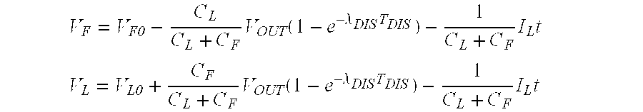
Referring to FIG. 5, one embodiment of a charge pump power output stage 44 (or “charge pump”) is shown for use with the power converter of FIG. 3. The power output stage 44 is operated in two phases: charge and discharge, (i.e., pump) as described above for the oscillator-controlled power converter 20 of FIG. 2. The power output stage 44 is coupled between the energy source 12 that provides an input voltage VS, and the load device 14 that accepts a current load IL. Unlike FIG. 2, no voltage regulator 22 is depicted. The power output stage 44 is configured with load capacitor CL, fly capacitor CF, and four power switches M1-M4 as described above for FIG. 2. In order to illustrate the advantages of dynamically controlling a charge pump in accordance with one aspect of the invention, the following analytical derivation describes how the power output stage 44 may be efficiently switched. The power controller 46 divides the operation of the charge pump into two phases: charge and discharge. Thus, the terms “charge” and “discharge” refer to the fly capacitor CF. During the charge phase, the input voltage VS charges the fly capacitor CF, and the load capacitor CL supplies power to the load. During the discharge phase, charge flows from the fly capacitor CF to both the load and load capacitor CL. Thus, the terms “charge” and “discharge” refer to the fly capacitor CF. Two parameters affect the operation of the charge pump:
1. ε—The fraction of the input voltage VS to which the fly capacitor CF is charged, where 0<ε<VS.
2. TDIS—The minimum amount of time that the fly capacitor CF is discharged to boost the output voltage VOUT.
The boundary conditions for the power output stage 44 that must be satisfied to supply the maximum load current IL, are shown in FIG. 6. The output voltage VOUT drops as the fly capacitor CF is charged during the charge phase. At the end of the following discharge phase, enough electrical charge must be transferred to increase the load voltage VOUT back to the reference voltage VREF.
For purposes of this analysis, it is assumed that the power switches M1-M4 and storage capacitors CF, CL will operate from an initially discharged condition (i.e., VOUT=0, VF=0) at time (t)=0, regardless of how low the input voltage VS is or whether a load device 14 is present. Furthermore, the analysis assumes a first and second control loop 56, 58 implementation wherein the state of charge is monitored for both the load capacitor CL and fly capacitor CF respectively. Moreover, a load voltage VL across the load capacitor CL will be used interchangeably with the output voltage VOUT.
During startup, the power output stage 44 goes through many charge-discharge phases until the output voltage VOUT charged on CL rises above a predetermined value (desired output voltage), or voltage reference, VREF. After CL has been fully charged (i.e., VOUT>VREF), the power output stage 44 will remain in the discharge phase until a load is applied, causing the output voltage VOUT to fall below the reference voltage VREF (VOUT<VREF), as depicted at the left-most portion of FIG. 6. A dead time delay TDEL occurs before a charge phase is initiated at time (t)=0. The fly capacitor CF is charged until its voltage VF reaches a fraction of the input voltage ε VS at time (t)=a. After CF has been charged, the power output stage 44 returns to the discharge phase for a minimum period of time given by TDIS, beginning at time (t)=b and ending at time (t)=c. This minimum time TDIS provides sufficient time for the discharge of the fly capacitor CF. After this minimum discharge time, the power output stage 44 remains in the discharge phase while VOUT>VREF. Since this analysis illustrates a maximum power capacity situation, VOUT is immediately below VREF at the time (t)=c. Thus, the reference voltage VREF has not been exceeded during the discharge phase, and the charge phase/discharge phase is performed again.
A dead time delay TDEL between time (t)=a and time (t)=b occurs between the charge and discharge phases with the switches M1-M4 all open to eliminate any possibility of a momentary short circuit (i.e., an intervening delay to mitigate transconductance). For example, if switches M1 and M2 are closed at the same time, then the positive terminal 30 of the energy source 12 is shorted to the positive output terminal 42. If switches M1 and M4 are closed at the same time, the fly capacitor CF is shorted, degrading performance and possibly causing damage due to heat generation.
This analysis illustrates that an opportunity exists to switch the switch matrix at an optimal rate. First, if the output voltage VOUT exceeds the reference voltage VREF after the minimum discharge time TDIS, an opportunity exists to remain in the discharge phase. Unnecessary (and thus inefficient) switching back to the charge phase is delayed as appropriate. Similarly, sensing when the fly capacitor CF is charged similarly avoids unnecessary switching due to a charge time TCHG that is too short or avoids a missed opportunity to transfer more charge when charge time TCHG is too long.
For applications utilizing a battery as an energy source 12, the power output stage 44 of the invention advantageously may satisfy several performance constraints over the lifetime of the battery while maximizing battery efficiency. Increasing the efficiency will extend the service life of the battery. The performance constraints include the minimum value for the peak output load current IL that can be supplied without exceeding a limit on the allowable output voltage ripple VRIP. The output voltage ripple VRIP is the range of the fluctuation of the output voltage VOUT. A maximum acceptance value for the operating frequency (i.e., rate of cycling between charge and discharge phases) is also required to minimize noise in audio applications. If the operating frequency is too high, charge consumed by the power output stage 44 will reduce the efficiency of the charge pump. Some of the objectives are conflicting. For example, although a high operating frequency reduces the output voltage ripple VRIP, it also reduces the efficiency of the power output stage 44. Optimizing thus requires finding a is subset of parameters for which the performance constraints can be met. If there is adequate margin, the design can then be optimized by selecting the values within this subset that maximize the efficiency of the design. This will provide advantages for a power converter 40, such as increased battery life while satisfying the output performance constraints. The following illustrates optimizing the power output stage 44 with power switches M1-M4 and typical power requirements.
Starting with the equations for the circuit depicted in FIG. 5, the loop currents and node voltages can be found as a function of the load current IL and fixed parameters during the charge and discharge cycles of the power output stage 44. The fixed parameters include the input voltage VS, resistance of power switches M1-M4, capacitance values CF and CL, and the reference voltage VREF. Although the input voltage VS may change over time, the worst case analysis assumes that it is fixed at its lowest expected value during its lifetime. Some of the other fixed parameters are fixed in that they are selected for a given design (e.g., size of capacitors CF, CL, type of power switch M1-M4, etc.). The variable parameters are ε and TDIS. By evaluating boundary conditions, specific solutions for the equations can be found. The boundary conditions are selected such that the load current IL is the maximum possible for the current set of fixed and variable parameters. The solutions for the differential equations can then be solved for the maximum load current IL that can be supplied for a specific set of parameters. By varying the parameters, the maximum load current IL over a range of these values can be found. The maximum load current IL is a continuous function of the parameters. This implies that if the largest value for the maximum load current IL exceeds the minimum acceptable value, a subset of parameters will also satisfy this condition. The efficiency of the power output stage 44 can then be maximized over this subset of parameter values, providing efficiency while satisfying the minimum performance constraints.
During the discharge phase, the voltage across CF and CL are: V F = V F0 - C L C L + C F V OUT ( 1 - e - λ DIS T DIS ) - 1 C L + C F I L t V L = V L0 + C F C L + C F V OUT ( 1 - e - λ DIS T DIS ) - 1 C L + C F I L t
Figure US06643151-20031104-M00001
where: V OUT = ( V S + V F0 - V L0 ) - C F C L + C F I L R DIS λ DIS = C L + C F R DIS C L C F
Figure US06643151-20031104-M00002
and VFO and VLO are the initial fly capacitor voltage VFO and load voltages VLO at the start of the discharge cycle. When the fly capacitor CF is being charged, the load capacitor CL is being discharged. During the charge phase, the voltage across CF and CL are: V F = V F0 + ( V S - V F0 ) ( 1 - e - λ CHG T DHG ) V L = V L0 - 1 C L I L t
Figure US06643151-20031104-M00003
where: λ CHG = 1 R CHG C F
Figure US06643151-20031104-M00004
The initial fly and load voltages VF, VL are at the start of the charge phase.
This set of four equations also has four unknown values: VF, VL, IL, and TCHG, and therefore will have a unique solution (if one exists). The algorithm for finding this solution using the boundary conditions illustrated in FIG. 6 is as follows. A charge time TCHG is found by evaluating the following equation: 0 = A ( 1 - e λ CHG T CHG ) + B ( T CHG + T DIS + 2 T DEL ) D + C T CHG
Figure US06643151-20031104-M00005
where: A = ( 1 - ɛ ) V S B = C L C L + C F [ ( 1 + ɛ ) V S - V REF ] ( 1 - e - λ DIS T DIS ) C = 1 - C F C L + C F ( 1 - e - λ DISs T DIS ) D = C L C L + C F C F C L + C F R DIS C F ( 1 - e - λ DIS T DIS ) + C L C L + C F T DIS + 2 C T DEL
Figure US06643151-20031104-M00006
The value of TCHG that solves this equation must be constrained to be greater than zero to be valid. Solutions will not exist for all combinations of the fixed and variable parameters.
With TCHG known, the maximum load current IL for the current value of the parameters is given by: I L = C L C F C L + C F [ ( 1 + ɛ ) V S - V REF ] ( 1 - ɛ - λ DIS T DIS ) / [ 1 - C F C L + C F ( 1 - ɛ - λ DIS T DIS ) ] ( T CHG + 2 T DEL ) + C L C L + C F [ C F C L + C F R DIS C F ( 1 - ɛ - λ DIS T DIS ) + T DIS ]
Figure US06643151-20031104-M00007
The voltage across the fly capacitor VF at the end of the discharge phase is: V F0 = ɛ V S - C L C L + C F [ ( 1 + ɛ ) V S - V REF ] ( 1 - ɛ - λ DIS T DIS ) + 1 C L + C F [ C L C L + C F R DIS C F ( 1 - ɛ - λ DIS T DIS ) - ( T CHG + 2 T DEL ) ( 1 - ɛ - λ DIS T DIS ) - T DIS ] I L
Figure US06643151-20031104-M00008
The lowest voltage reached by the load voltage VL at the beginning of the discharge phase is: V L0 = V ref - 1 C L I L ( T CHG + 2 T DEL )
Figure US06643151-20031104-M00009
The difference between this and the reference voltage VREF is the ripple VRIP:
V RIP =V REF −V LO
The operating frequency (i.e., frequency of the voltage ripple) for this set of parameters is: f = 1 T CHG + T DEL + 2 T DEL
Figure US06643151-20031104-M00010
The peak input voltage is also interesting to evaluate, and can occur at either the beginning of the charge phase, or during discharge. Because the load current IL is assumed to be constant, the peak input current IS during discharge occurs at the beginning or end of this phase. The peak current during the entire cycle is the maximum of these values: I _ S = max { I _ CHG , I _ DIS 1 , I _ DIS 2 } I _ CHG = V S - V F0 R chg I _ DIS 1 = ( 1 + ɛ ) V S - V L0 R dis I _ DIS 2 = ( 1 + ɛ ) V S - V L0 R DIS ɛ - λ T DIS + C F C L + C F ( 1 - ɛ - λ T DIS ) I L
Figure US06643151-20031104-M00011
Referring to Table 1, the maximum load current IL, voltage ripple VRIP, peak input current {overscore (I)}L, and the operating frequency were evaluated as an illustration for a combination of fixed parameters including the reference voltage VREF and the input voltage VS at which the charge pump is expected to operate reliably, and the fly (CF) and load (CL) capacitance values. In this illustration of a power output stage 44, the resistance of the capacitors CL, CF is ignored. The time delay TDEL used to prevent all switches M1-M4 from being closed at the same time was fixed at 0.25 μSec. Two time delays TDEL occur in each charge-discharge discharge cycle.
TABLE 1
Charge Pump Operating Points for Moderate Capacitance Values.
Optimized Charge Pump
CF = 22 μF, CL = 220 μF, Vref = 1.2 V, Vs = 0.8 V
Operating RCHG = RDIS (Ω)
Point 0.1 0.2 0.3
ε 0.8490 0.8306 0.8214
TDIS (μSec) 1.8571 3.0204 3.9898
IL (mA) 838.17 447.09 306.12
Vrip (mV) 8.9955 7.1155 6.2130
{overscore (I)}S (A) 2.8818 1.3580 0.8779
freq (kHz) 288.18 153.33 118.275
The series resistances encountered during the charge (RCHG) and discharge (RDIS) phases have the most significant effect on the maximum current capacity of the power output stage 44, as shown by the three operating point columns in Table 1. Although larger fly (CF) and load (CL) capacitors improve this capability, the amount of improvement is mitigated as their resistance increases. Increasing the capacitor values appears to have a greater proportional effect on reducing the output voltage ripple VRIP, rather than the current capacity.
What the analysis described above shows is that a power output stage 44 may be dynamically controlled to achieve a desired output voltage VOUT given that the output voltage is sensed as feedback.
Typical “electronic” capacitors (dielectric between conductors, e.g., tantalum polymer), widely used in electronic devices, are characterized by self discharging within microseconds to milliseconds, and having a cycle life of 1-10 million charge cycles. The disadvantage of the short self-discharge time for electronic capacitors means that oscillator-based charge pumps 20 must operate at duty cycles that are between the rate in which the electronic capacitor can be charged and discharged and the rate at which the electronic capacitor will self-discharge. Consequently, known oscillator controllers 26 for charge pump output stages 24 do not allow for charge pump operating frequencies in the 50-200 Hz range. At lower demand levels, the charge pump would advantageously operate below 1 Hz.
Consequently, known oscillator-based charge pumps 20 cannot take advantage of ultra-capacitors and similar high storage devices that have self-discharge times measured in weeks or months. An ultra-capacitor is an electrochemical double layer capacitor that stores energy electrostatically by polarizing an electrolytic solution. There is no chemical reaction involved in its energy storage physics. Consequently, the ultra-capacitor is extremely bi-directional (recoverable) and can thus be charged and discharged thousands of times, unlike comparable storage methods like electrochemical batteries. An example of a suitable ultra-capacitor is the PS-10 available from Maxwell® Technologies, San Diego, Calif.
It should be appreciated that the term “ultra-capacitor” is meant to encompass a number of types of large capacitors generally characterized as having a high efficiency due to relatively low charge leakage. Thus, “ultra-capacitor” includes double layer electrolytic capacitors (often known as super capacitors, ultra capacitors, and power capacitors), as well as pseudo capacitors.
In accordance with another aspect of the present invention, charge pumps incorporating ultra-capacitors for the fly capacitor CF and load capacitor CL are capable of providing 5 W of electrical power or more, for which rate an operating frequency of 50-200 Hz would be appropriate.
The dynamic controller 50 of one embodiment of the invention, as will be described in more detail below, is capable of operating at the frequencies of the oscillator-based charge pumps 20; however, the dynamic controller 50 is also capable of operating at extremely low operating frequencies. Consequently, the dynamic controller 50 may take advantage of the additional storage capabilities of ultra-capacitors.
Sub-One Volt Power Converter
Referring to FIG. 7, one embodiment of a dynamically controlled power converter 40A in accordance with the principles of the invention is depicted in a top-level block diagram form. As will become apparent in the discussion below, this illustrative embodiment allows for a step up or step down of an input voltage VS from an energy source 12 to a regulated output voltage VOUT by dynamically controlling the noninverting charge pump power output stage 44A. The power converter 40A may also operate at an input voltage VS below one (1) volt.
Specifically, power switches M1-M4 adapted to respond to low threshold switching signals S1 and S2. Moreover, as will become apparent below, the power converter 40A may readily be implemented as an integrated circuit and thus be of small size and cost.
The illustrative power converter 40A of FIG. 7 includes a power controller 46A and the power output stage 44A similar to one described above for FIG. 5. The power controller 46A includes a comparator 94 responsive to VOUT dropping below a reference voltage VREF to generate a switching signal. Advantageously, the comparator 94 is further responsive to the voltage of the fly capacitor VF and the input voltage VS for controlling the duration of the charge phase. Specifically, a comparator input switching circuit 98 enables the same comparator 94 to be is used during both the charge and discharge cycles as follows.
During the charge phase, a predetermined fraction of the input voltage εVS is coupled to a first comparator input 100 via comparator input switch M9 that closes in response to charge cycle switch signal S1. A VS divider 102 interposed between switch M9 and the energy source 12 provides the predetermined fraction ε and the resulting reductions of VS. The fly capacitor voltage VF is coupled to a second comparator input 104 via comparator input switch M10 also in response to charge cycle switch signal S1. The comparator then generates a switching signal when the fly capacitor voltage VF reaches a predetermined fraction of the input voltage εVS.
During the discharge phase, the reference voltage VREF is coupled to the first comparator input 100 via comparator input switch M11 in response to discharge cycle switch signal S2. Also, a predetermined fraction of VOUT provided by VOUT divider 108 is coupled to the second comparator input 104 by comparator input switch M12 in response to switch signal 52.
With regard to the scaling of various inputs to the comparator 94, it should be apparent to those skilled in the art that various combinations of scaling may be appropriate for specific applications. For instance, the illustrative example is based on a step up power converter configuration and a voltage reference VREF that is relatively low. Thus, the VOUT divider 108 allows scaling down the VOUT as needed to use a single reference voltage to achieve a range of desired output voltages VOUT. In applications where the VOUT is lower than the reference voltage, a VOUT multiplier may be used instead or a divider used to scale down the output from the voltage reference 96 to a desired reference voltage VREF. Similarly, other variations would be apparent for step down power converters. Moreover, a second comparator may be used in addition to comparator 94 if necessary.
The switching command from the comparator 94 is received by a timing controller 112 for generating charge switch signal S1 and discharge switch signal S2. Advantageously interposed between the comparator 94 and the timing controller 112 is a delay 114 for causing a hysteresis in switching for purposes such as avoiding unnecessary switching and to reduce the effects of EMI emissions from higher operating frequencies.
A bootstrap start-up circuit 116 is depicted in FIG. 7 for initiating operation of the power output stage 44A when it is discharged and the dynamic controller 50A has not taken control of the power output stage 44A, as will be described in more detail with regard to FIG. 11.
A start-up circuit 116 is necessary for integrated circuit embodiments of the present embodiment in which semiconductors may latch to ground during a cold start (i.e., initially discharged load capacitor CL), preventing the dynamic controller 50A from taking control of the power output stage 44A. More generally, the start-up circuit may shorten the time required during a cold start until operating at the desired output voltage VOUT.
The start-up circuit 116 is depicted as coupling the positive terminal 30 of the energy source 12 to the first terminal 31 of the fly capacitor CF rather than directly to the first terminal 32 of the load capacitor CL. However, due to a choice of a normally closed switch M2, it should be appreciated that the start-up circuit is effectively coupled to the load capacitor CL in start-up (cold start) situations, as is discussed below.
A by-pass control circuit 118 included in the power controller 46A may be used during certain situations such as a transient high load beyond the capacity of the power converter 40A. The transient high load is characterized by a decrease in the output voltage (voltage droop) that is of a predetermined magnitude to require additional capacity. Thus, the by-pass circuit 118 may compare VOUT to the reference voltage VREF. When a voltage droop is detected in VOUT, the by-pass circuit 118 may generate a by-pass switch signal SB for by-pass switch MB that responds by coupling the positive terminal 30 of the energy source 12 directly to the output terminal 42. Similarly, the by-pass circuit 118 may respond to an impending failure of the power converter 40A due to low input voltage wherein extending service life is best served by removing the power consumption of the power converter 40A. Thus, the by-pass circuit 118 also compares the input voltage VS to the reference voltage VREF and operates switch MB accordingly.
The operation of the power converter 40A of FIG. 7 is illustrated in the flow diagrams of FIGS. 8-10. Referring to FIG. 8, the power converter operation 130 begins with the storage elements discharged, and thus a start-up operation 132 is performed to prevent latch up to ground in integrated circuit implementations, as will be described in FIGS. 9 and 11. After start-up operation 132, the power converter operation 130 moves into a dynamic operation 134, as will be described with regard to FIG. 9.
Dynamic operation 134 generally continues until interrupted, as represented in block 136 by a determination as to whether an output voltage VOUT droop has occurred, and if not, dynamic operation 134 continues. A voltage droop in VOUT is a drop in the output voltage VOUT indicating a large transient load that may exceed the capability of the power converter 40A. If in block 136 VOUT droop is detected, then a transient by-pass is performed electrically coupling the output terminals to the energy source for a period of time (block 138) as discussed above. In some applications consistent with the invention, the transient by-pass electrically uncouples the power converter 40A from the energy source 12 and the output terminals 42, 43. An advantage of uncoupling includes avoiding discharging of the power output stage 44A that would result in a recovery period after the transient ends. In other applications consistent with the invention, the transient by-pass does not uncouple the power converter 40A from the energy source 12 and the output terminals 42, 43 so that the power converter 40A contributes to providing the power demanded by the load device 14.
If the output voltage still remains low (block 140), then the by-pass may be placed in a latched state (block 142). If in block 140 VOUT has recovered, then another protective feature is performed in block 144 by making a determination as to whether a current overload condition exists. For example, the energy source may have a safety limitation on the amount of current that can be provided, perhaps for a certain duration. Alternatively, the load device 14 drawing the output current may be in a failure mode that is signaled to the power converter operation 130. Thus, if in current overload (block 144), the output terminal is disconnected from the energy source (block 146). If, however, in block 144 there is no current overload, then in block 148, a determination is made as to whether or not the controller is off. This represents situations where the various protection measures may result in a situation where the power converter needs to be restarted. Thus, if the controller is off (block 148), then the power converter operation 130 returns to start-up operation (block 132), else to dynamic operation (block 134).
It should be appreciated that a sequential flow diagram is shown in FIG. 8 illustrates various protection and modes that may be performed independently and continuously or that various combinations of protective features may be included consistent with the invention.
Referring to FIG. 9, the start-up operation 132 referenced in FIG. 8 is depicted in flow diagram form. An advantage of this start-up operation 132 includes illustrating how a power converter 40A in accordance with the invention may be started with less than one volt of input voltage. This is especially desirable for integrated circuit applications wherein a discharged storage capacitor, such as the load capacitor CL, may otherwise result in an inoperative power controller 46A. Moreover, the start-up operation 132 suggests use of the invention as a low output demand alternative charge pump wherein the power consumed by the overall power converter may be reduced.
Typical oscillator-based power converters 20 incorporate a bootstrap external large power Schottky diode electrically coupled from the energy source 12 to the load capacitor CL. The Schottky diode conducts when the load capacitor voltage VL is low, to begin charging the load capacitor CL, as well as providing power to the load device 14. Without the additional Schottky diode, the load device 14 would tend to prevent the load capacitor CL from charging due to latch-to-ground tendencies of typical integrated circuit switch matrices 48.
Adding the Schottky diode prevents desirable miniaturization of the oscillator-controlled power converter 20. In addition, the Schottky diode consumes power during normal operation of the oscillator-controlled power converter 20, thereby reducing efficiency.
Therefore, it is desirable to start the dynamically controlled power converter 40A without detrimentally affecting efficiency during normal operation. It is also desirable to do so in a way that may be integrated with the power converter 40A without external components.
The start-up operation 132 begins with an initial condition in block 150 that a load is already applied to the power converter and in block 152 that an input voltage is available to the power converter. Then a determination is made as to whether the power controller is off and not controlling the power output stage (block 154). If the power controller is on (block 154), then a small start-up capacitor CQPUMP is floated (block 156) and start-up operation 132 is done.
If in block 154 the controller is off, then a start-up switch is closed to provide input voltage VS to the start-up capacitor CQPUMP (block 158) and the start-up capacitor CQPUMP is referenced to ground (block 160). When the start-up capacitor CQPUMP is charged (block 162), it is discharged into a storage capacitor (e.g., load capacitor) (block 164) and the start-up circuit including start-up capacitor CQPUMP is uncoupled from the switch matrix of the power converter (block 166). Then, the start-up operation 132 returns to block 154 to see if this start-up cycle was sufficient to activate the controller and subsequent start-up operation cycles repeat as necessary.
Referring to FIG. 10, the dynamic operation 134 referenced in FIG. 8 is illustrated in flow diagram form. First, the fly capacitor is switched into parallel with the input voltage VS so that the fly capacitor may be charged (block 170). When the fly capacitor voltage VF exceeds some predetermined fraction of the input voltage VS (e.g., 80% of VS) (block 172), then the charge phase ends by uncoupling the fly capacitor CF from being in parallel with the input voltage VS (block 174) and delaying for a dead time delay TDEL (block 176).
The discharge cycle then begins in block 177 by determining whether the dynamic operation 134 is for step up or step down operation. If stepping up, then during discharge phase, the fly capacitor voltage VF is added to the input voltage VS whereas, if stepping down, the fly capacitor voltage VF is used alone. This selection may be predetermined and preset rather than being determined during each phase of the dynamic operation 134, although these additional determinations advantageously allow for adjusting the output voltage VOUT as desired such as by changing the reference voltage VREF.
Thus, in block 177 a determination is made as to whether the reference voltage VREF is less than the input voltage VS (i.e., stepping down operation). If yes, then the fly capacitor CF alone is placed across the load capacitor CL (block 178). Otherwise, the input voltage VS and the fly capacitor CF are placed in series across the load capacitor CL (block 179). After either block 178 or 179, a minimum discharge time delay TDIS is then performed to allow full discharge of the fly capacitor CF without respect to the output voltage VOUT (block 180).
Then, the dynamic operation 134 waits in this state while the output voltage VOUT is greater than the reference voltage VREF (block 182). This is due to the non-compensated nature of the comparator. If the amount of charge transferred during the preceding charge/discharge cycle is insufficient to charge the load capacitor CL for VOUT to exceed VREF, another subsequent charge/discharge cycle immediately is needed. In other instances, the preceding charge/discharge cycle is sufficient. Thus, the dynamic operation 134 then may continue waiting for a period of time until the load device or self-discharge of the load capacitor discharges the load capacitor sufficiently. When VOUT is not greater than VREF, the fly capacitor CF is uncoupled from the load capacitor CL (block 184), which includes uncoupling the input voltage VS from the load capacitor CL if stepping up. Then, another dead time delay TDEL is imposed (block 186), and the cycle repeats by returning to the charge phase of block 170.
It should be appreciated that for clarity the aforementioned dynamic operation 134 begins with charging the fly capacitor CF until such time as a discharge phase is warranted. In the illustrative embodiment, however, the charge phase is, in effect, a nested operation within the discharge phase. Specifically, the power converter initiates and remains in a discharge phase until such time as additional charge is needed (e.g., VOUT drops below VREF). Then a charge phase is performed. As soon as completed, then the discharge phase begins again after the requisite described delays. Thereafter, the power converter 40A remains in the discharge state again waiting for more needed charge.
With reference to FIG. 11, an integrated power output stage 44A for the power converter 40A of FIG. 7 is advantageously illustrated by an integrated circuit implemented with a 0.35 micron double salicide process (two metal, two poly salicide) utilizing MOSFET transistor switches capable of low threshold (e.g., sub-one volt) control, as described in the following co-pending and commonly owned application filed on Mar. 22, 2000: U.S. Ser. No. 09/532,761, entitled “Lateral Asymmetric Lightly Doped Drain MOSFET”, naming Ying Xu et al., which is hereby incorporated by reference. In addition to having a low threshold control, the disclosed MOSFET devices have a low on-resistance, directly contributing to the efficiency of the switch matrix 48 used in accordance with the invention.
The power switches M1-M4, as well as the by-pass switch MB have scaleable current capability to the desired peak output current by incorporating an array of low-threshold MOSFET devices, although represented as a single transistor in FIG. 11. The MOSFET power switches M1-M4 are advantageously designed for low on-resistance and high off-resistance for efficient operation of the switch matrix 48, as described in the above referenced application.
Generally, n-type MOSFET devices are chosen for being smaller to fabricate, faster to switch, and normally off without a gate voltage. In some instances, p-type MOSFET switches are advantageously used, however. First, as will become more apparent below, using a p-type power switch M2 between the first terminal 31 of the fly capacitor CF and the first terminal 32 of the load capacitor CL allows for a sub-one volt progressive start-up circuit 116 in accordance with one aspect of the invention that needs to only bias one power switch M1 in order to start the power converter 40A.
The start-up circuit 116 includes a p-type MOSFET startup switch MS configured to activate the start-up circuit 116 when the power output stage 44A is discharged. The various signals (e.g., S1, S2, S2N . . . ) for controlling the switching are discussed further herein below. The drain of MS is coupled to the input voltage VS and the gate and source are both coupled to the first terminal 31 of the fly capacitor CF. The two power switches M3, M4 coupled to the second terminal 34 of the fly capacitor CF are n-type and thus open, so the fly capacitor CF is floating in this situation. However, the power switch M2 is a p-type transistor as mentioned and is thus closed with the power controller 46A initially unpowered in this situation. Consequently, the start-up switch MS also has its gate and source coupled to VOUT that is initially zero. Thus the gate of start-up switch MS is grounded, and the start-up switch MS begins to conduct the input voltage VS to the load capacitor CL.
However, the current capability of this one small MOSFET is insufficient to charge the load capacitor CL. Therefore, the start-up switch MS is used indirectly to close power switch M1 so that the input voltage VS will be provided to the load capacitor CL. Specifically, the input voltage from the source of the start-up switch MS is coupled to the gate of n-type switch M13. Switch M13 is closed due to the input voltage VS from switch MS. When switch M13 closes, the input voltage VS at the drain is passed to the source, which in turn is coupled to a first terminal 190 of a start-up capacitor CQPUMP. The second terminal 192 of the start-up capacitor CQPUMP is coupled to a transistor pair M14, M15 configured to ground the second terminal 192 of the start-up capacitor CQPUMP when the power controller 46A is inoperative. Otherwise, the transistor pair M14, M15 is configured to float the second terminal 192 of the start-up capacitor CQPUMP. Specifically, the second terminal 192 of the start-up capacitor CQPUMP is coupled to the drain of p-type switch M15 and to the source of n-type switch M14. Switch M15 has its source grounded and has its gate biased by a negative bias to open switch M15 when the power controller 46A is operating. Therefore, when the power controller 46A is operating, the second terminal 192 of the start-up capacitor CQPUMP is disconnected from ground. Switch M14 has its drain coupled to the input voltage VS and has its gated biased by a positive bias to close switch M14 when the power controller is operating.
Referring to FIG. 12, a circuit is shown that is suitable for the power converter 40A of FIG. 7. FIG. 12 illustrates one circuit embodiment for biasing the comparator 94 to perform comparisons during the charge phase and during the discharge phase. During the charge and discharge phases, the circuit will have previously been started and power controller 46A will be operating for generating the switching signals (e.g., S1, S2, etc.). During the charge phase with S1 closing M9 and M10, input voltage VS divider 102 reduces the input voltage VS by a predetermined fraction (e.g., 80%) for comparison with the fly capacitor voltage VF, as discussed for FIG. 7. During the discharge phase with S2 closing M11 and M12, VOUT divider 108 scales the output voltage VOUT for the correct comparison to the reference voltage from the voltage reference 96.
FIG. 12 also illustrates that the timing controller 112 of the power controller circuit 46A provides a plurality of signals P_S2NB, P_S2NA, S2, S2N, P_S1, S1, S1N, described in more detail below, to perform the equivalent to the charge switch signal S1 and the discharge switch signal S2. This plurality of signals is required for the illustrative embodiment due to the power switches M1-M4 requiring more current than the other switches, and power switches M2, M4 are p-type and thus switch more slowly than n-type power MOSFET power switches M1, M3. Certain delays are required in the signals to the respective gates in order to prevent transconductance wherein one or both of M1, M3 is closed at the same time as one or both of M2, M4.
Referring to FIG. 13, one embodiment of a voltage reference 96 is shown and is capable of sub-one volt input voltage VS operation in accordance with an aspect of the invention. A constant current circuit 200 powers a voltage reference-to-rail circuit 202, isolating the voltage reference-to-rail circuit 202 from changes in the input voltage VS. An output buffer 204 amplifies an unamplified reference voltage from the voltage reference-to-rail circuit 202. In order to temperature compensate the voltage reference-to-rail circuit 202, a parallel diode array Proportional to the Absolute Temperature (PTAT) circuit 206 biases the circuit 202.
Referring to FIGS. 14 and 15, one embodiment of a comparator 94 is depicted for the power controller 46A of FIG. 7. Differential amplifiers 206-210 are advantageously used since they are effective in rejecting common-mode signals. For example, common-mode signals may be induced noise on the inputs. Integrated circuit differential amplifiers have relatively low output gain. This has implications in two ways: non-linearity in an input transistor and in providing necessary current gain for later stages of the power controller 46A. For providing some cancellation of input non-linearity, a three differential amplifier combination is depicted, wherein the first differential amplifier 206 receives a V+ input at its negative input and V− at its positive input. A second differential amplifier 208 receives V− at its negative terminal and V+ at its positive terminal. The output of the first differential amplifier 206 is coupled to a negative terminal of a third differential amplifier 210 and the output of the second differential amplifier 208 is coupled to a positive input of the third differential amplifier 210. A fourth differential amplifier 212 is configured as a voltage follower buffer to increase the current of a comparator switching signal (Out+, Out−) from the third differential amplifier 210.
Referring to FIG. 16, one embodiment of a timing controller circuit 112 is depicted for the power controller 46A of FIG. 7. Basically, the timing controller circuit 112 is responsible for performing the necessary individual switch commands to reconfigure the power output stage 44A between charge and discharge phases. In addition, the timing controller circuit 112 for the power controller 46A must correctly phase paired switches and sequenced switches to avoid certain switch combinations. For example, neither of the charge phase power switches M1 and M3 should be closed at the same time as either of the discharge phase power switches M2 and M4. Otherwise, a cross conduction (or transconductance) occurs wherein, for example, the energy source 12 is momentary shorted to the output terminal 42, as discussed above.
Referring to FIG. 17, a timing diagram for the timing controller circuit 112 is depicted. Specifically, the S1 signal is the charge phase signal used internally by the dynamic controller 50. The S2 signal is the discharge phase signal used internally by the dynamic controller 50. The P_S2Nb signal is a higher current switch signal for a p-type MOSFET M2, delayed with respect to the S2 signal to prevent cross conduction, as well as inverted from S2 due to p-type MOSFET M2 opened by a positive voltage. The P_S2Na is a high power switch signal for a p-type MOSFET M4, delayed with respect to the P_S2Nb. The P_S1 signal is a higher current version of S1 for the power MOSFET switches M1, M3. The S2N signal is an inverted version of the S2 signal for the start-up circuit 116, specifically switch M14. The S1N signal is an inverted version of S1 for the start-up circuit 116, specifically switch M15.
While the present invention has been illustrated by description of several embodiments and while the illustrative embodiments have been described in considerable detail, it is not the intention of applicants to restrict or in any way limit the scope of the appended claims to such detail. Additional advantages and modifications readily appear to those skilled in the art.
For example, although dynamically controlling a noninverting charge pump power output stage 44A has been discussed. Having the benefit of the instant disclosure, it would be apparent to those skilled in the art that it would be consistent with the invention to dynamically control an inverting charge pump power output stage.
A power converter 40A consistent with the invention may be incorporated in a wide range of products. For example, a power converter 40A taking advantage of the small size achievable with integrated circuits and low power consumption properties described above may advantageously be incorporated into a battery package to enhance battery service life and energy and amplitude on demand.
Moreover, a power converter 40A consistent with the invention, whether incorporated inside an energy source 12 or in a load device 14 utilizing an energy source 12, would improve or enable a wide range of portable electronic devices 10. For example, the reduction in size and weight of an energy source 12 would allow less intrusive medical diagnostic, energy-delivery, or actuated medicine delivery devices, whether worn or implanted.
In addition, portable electronic currently powered by batteries or similar energy sources 12 may be improved by incorporating the power converter in accordance with the invention. In portable communication devices and portable audio devices, for instance, improved service life may be obtained through the increased efficiency, and performance may be enhanced by lowering the power converter 40A operating frequency, and thus the noise, when allowed to do so by a decreased demand.
Also, a largely or fully integrated power converter 40A consistent with the invention would provide a sufficiently small efficient power supply for memories, logic circuits and other integrated devices. For example, the power converter 40A may be embedded into a portion of an integrated circuit also containing a memory, logic circuit or other integrated device.
Furthermore, the aspects of the invention related to dynamically adapting to the input voltage, especially with regard to a low input voltage, allow for applications wherein the input voltage is volatile or otherwise unsuitable for generally known power converters. For example, photovoltaic cells provide power in relation to the surface area and the amount of incident radiant energy. Consequently, devices using photovoltaic cells may often be inoperable due to insufficient light, may have to limit functionality to remain within the typical amount of available power, and/or have to increase the surface area devoted to photovoltaic cells. Thus, a power converter 40A may allow for smaller photovoltaic cells and use in a wider range of lighting conditions.
As an additional further example, a single fly capacitor CF and load capacitor CL has been illustrated for clarity. It should be appreciated by those skilled in the art that power converters 40A consistent with the invention may include a plurality of fly capacitors CF and/or a plurality of load capacitors CL. Moreover, the fly capacitor CF and/or load capacitor CL may comprise various storage devices for electrical and magnetic energy.
As another example, a power converter 40A consistent with the invention may be incorporated in a wide range of products. For example, a power converter 40A taking advantage of the small size and low power consumption (i.e., efficiency) properties described above may advantageously be incorporated into a battery package to enhance battery service life and energy and amplitude on demand. Incorporating the power converter 40A would be accomplished in manner similar to that disclosed in the following co-pending and commonly owned applications all filed on Apr. 2, 1998: U.S. Ser. No. 09/054,192, entitled PRIMARY BATTERY HAVING A BUILT-IN CONTROLLER TO EXTEND BATTERY RUN TIME, naming Vladimir Gartstein and Dragan D. Nebrigic; U.S. Ser. No. 09/054,191, entitled BATTERY HAVING A BUILT-IN CONTROLLER TO EXTEND BATTERY SERVICE RUN TIME naming Vladimir Gartstein and Dragan D. Nebrigic; U.S. Ser. No. 09/054,087, ENTITLED BATTERY HAVING A BUILT-IN CONTROLLER, naming Vladimir Gartstein and Dragan D. Nebrigic; and U.S. Provisional Application Serial No. 60/080,427, entitled BATTERY HAVING A BUILT-IN CONTROLLER TO EXTEND BATTERY SERVICE RUN TIME, naming Dragan D. Nebrigic Milan M. Jevtitch, Vig Sherrill, Nick Busko, Peter Hansen, and William Millam. All of the aforementioned applications are hereby incorporated by reference in their entirety.
Three-state Charge Pump Control
In other versions consistent with the invention as discussed herein, dynamic control of a charge pump may maintain the fly capacitor voltage and/or the load capacitor voltage within a predetermined voltage ripple band. The advantages of charging and discharging the fly capacitor within a predetermined voltage ripple include enhancing efficiency. The fly capacitor is utilized within a voltage region in which the rate of charge transfer and the internal losses during transfer are optimized. Switching losses are mitigated by optimizing the charge transfer during each charge/discharge cycle of the fly capacitor. Similarly, one of the advantages of maintaining the voltage across the load capacitor within a predetermined voltage ripple band is for improved efficiency.
The voltage ripple may be defined in terms of the source voltage VS (e.g., battery voltage VBAT), with two scaled thresholds of the battery voltage used for defining the fly capacitor voltage ripple band (e.g., αVBAT, βVBAT). However, the battery voltage VBAT declines due to the internal resistance of the battery, especially during peak loads and during the latter portions of the service life of the battery. Consequently, the fly capacitor voltage ripple band would also become lower. Since the resistance in the switches M1-M4 and the ESR of the capacitors CL and CF is low compared to the internal resistance of the battery, this voltage drop in the battery can cause stability problems in the circuit. Consequently, embodiments consistent with aspects of the invention use a fixed voltage reference to avoid instability problems.
However, there may be advantages to reducing the fixed voltage reference in response to a trend of reduced battery voltage. For example, a desired output voltage may become unachievable at a given reduced battery voltage with a voltage doubling charge pump. In response to sensing the reduced battery voltage, an additional charge pump stage or additional fly capacitor may be utilized to achieve the desired output voltage, while reducing the voltage thresholds used to trigger the charge/discharge cycles. One way of determining the trend in battery voltage is to sample the battery voltage during a no-load condition, such as during the time delay between charge and discharge cycles used to prevent cross-bar currents.
Referring to FIG. 18, a flow diagram illustrates the operation of one circuit for controlling the voltage ripple of the fly capacitor. First, a determination is made as to whether the fly capacitor is charged to the maximum fly capacitor voltage, i.e., VF≧VF,MAX (block 200). If not, the fly capacitor is charged until the maximum fly capacitor voltage is reached (block 202). When the fly capacitor is sufficiently charged, the fly capacitor is uncoupled from the source voltage and the load capacitor (block 204) and is placed within what may be referred to as a wait state. This wait state becomes a third state of the charge pump in addition to the charge and discharge states. With the fly capacitor charged and waiting to be deployed, delay is avoided (i.e., the delay of having to charge the fly capacitor after the output voltage is sensed as dropping too low). Thus, the power capacity of the charge pump is increased. In addition, in certain charge pump configurations, it is advantageous to have the load capacitor provide the output voltage with the source voltage and fly capacitor uncoupled (e.g., step-down configuration). Therefore, the wait state incorporated in accordance with one aspect of the invention is advantageous in these regards.
When the fly capacitor is in the wait state, a determination is made in block 206 as to whether the output voltage is less than or equal to the reference voltage, i.e., VO<VREF. If the output voltage is not less than or equal to the reference voltage, the fly capacitor is not necessarily needed at the output and the controller remains in the wait state (block 204). Once the output voltage does drop to the reference voltage or below (block 206), then the fly capacitor is coupled to the output and placed into a discharge state (block 208). The fly capacitor remains in the discharge state until a determination is made (block 210) that the fly capacitor voltage VF is less than the minimum fly capacitor voltage VF,MIN (block 210). Once discharged to the bottom of the fly capacitor voltage ripple band at this minimum fly capacitor voltage, then control passes back to block 202 to recharge the fly capacitor and to be prepared for the next charge-wait-discharge cycle in accordance with the invention.
Although not depicted in FIG. 18, it should be appreciated that a further determination could be made of both a maximum and minimum voltage reference for the output voltage so that voltage ripple in the output voltage could be further controlled. Thus, further hysteresis in the control could be employed.
Multiple-Output Power Converter
Another embodiment of a power converter 230 is depicted in FIG. 19, a block diagram of a circuit for providing selectable different output voltage levels. For example, levels of 1.8 V, 2.5 V, 3.0 V, 3.3 V, and 5.0 V are shown. It should be appreciated that other voltage levels are contemplated, such as lower voltages (e.g., 1.2 V, 1.5 V) as well as higher voltage levels (e.g., 7.0 V).
Each integral output stage 232 a-232 e for the various voltage levels may be a step-up or step-down charge pump power output stage as described above, with respective fly capacitors CF1-CF5 and load capacitors CL1-CL5. Five levels and associated output stages are shown in FIG. 19.
The dynamic control for each output stage 232 a-232 e is provided by a multi-output controller 234. The multi-output controller 234 receives a bandgap voltage reference 236 for scaling a reference voltage VREF to the various threshold levels necessary to control each output stage 232 a-232 e. The multi-output controller 234 is also responsive to an enable bus 238 to selectively turn on each output stage 232 a 14 232 e. The multi-output controller 234 provides charge and discharge switch signals to the respective output stages 232 a-232 e in accordance with the invention, depicted as a signal bus S1 1-5 and S2 1-5, respectively. The multi-output controller 234 generates these charge/discharge signals in response to fly capacitor voltages VF1-VF5 and the five output voltages (i.e., 1.8 VOUT-5.0 VOUT).
Referring to FIG. 20, a circuit for one example of the power output stages 232 a-232 e of FIG. 19 is shown, similar to that described for FIG. 5 above. The fly capacitor CF, which is coupled between nodes Vn FLY-HIGH and Vn FLY-LOW, and the load capacitor CL, which is coupled from node VO N to ground, are not shown.
The power MOSFETS M1A, M2A, M1B, and M2B shown in FIG. 20 correspond to switches M1, M2, M3 and M4 described above. Additionally, a p-type MOSFET switch M3 couples the source voltage (VCC) to the output when the multi-output controller 234 is deactivated in order to charge the load capacitors CL1-CL5 during start-up. The S3 n signal would be generated by the multi-output controller 234 thereafter when the output power stage 232 a-232 e is being operated. As discussed above, depending upon the type of MOSFET used (e.g., p-type, n-type), the control signals for some switches may be inverted or delayed with respect to the signals for other switches. (e.g. S1, S1 n, S2, S2 n, etc.)
Referring to FIG. 21, a block diagram is depicted for an output controller 234 a for one channel or voltage level (e.g. 1.8V) of the multi-output controller 234. The voltage ripple control of the fly capacitor voltage VF 1 is accomplished by switching between two scaled thresholds αVBAT, βVBAT based on the battery voltage VBAT being compared at comparator 250 to the fly capacitor voltage VF. The voltage ripple control of the output voltage VO across the respective load capacitor is accomplished by switching between two scaled thresholds αVREF, βVREF based on the reference voltage VREF as compared at comparator 252 to the output voltage VO 1. The results of the switched comparisons are provided to the switch logic and crossbar delays circuit 254, which in turn produce the charge and discharge signals S1 1 and S2 1. An input multiplexer (MUX) 256 controls the switching between the thresholds in response to whether the controller 234 a is currently in the charge or discharge mode. A signal S3 1 from the switch logic and crossbar delays circuit 254 advantageously allows for start-up, as described above for FIG. 20.
Depending on the input voltage or input voltages (VIN), one or more of the output stages 232 a-232 b may be permanently configured as step up (boost) or step down (buck) or reconfigurable step up/step down. For the latter, the output controller 234 n includes a comparator 258 sensing whether the battery voltage VBAT is above or below the reference voltage VREF, with the result provided to both the input MUX 256 and switch logic and crossbar delays circuit 254.
Referring to FIG. 22, a logic diagram is depicted for one embodiment of an output controller, such as controller 234 a of FIG. 21. In this version, the switched comparisons are performed by performing the comparisons with four comparators 261-264 continuously, and by using downstream switching in a switching logic control circuit 270, which outputs are passed to an output section 280.
The S3 n output is shown as a 50 msec delayed output from a three input AND gate with inputs of the power up (PUP) signal that is a filtered version of the source power VCC, of a comparison of the VO N with the reference voltage VREF, and of a comparison of the reference voltage VREF with the source voltage (VCC). Thus, the start-up charging of the load capacitor CL using S3_n will be shutoff 50 msec after the reference voltage stabilizes with respect to the source voltage (VCC) and output voltage VO N.
Referring to FIG. 23, a power up circuit is depicted for producing the power up (PUP) signal. In particular, the source voltage VCC is provided to one input of an AND gate. The first and second inputs of the AND gate are coupled via a resistor R31. The second input is also coupled to ground by capacitor C1. Consequently, PUP will go high after the source voltage VCC has stabilized since the second input sees a low-pass filtered version of the source voltage VCC.
Referring to FIG. 24, a pin-out depiction of a multiple-output power converter 230 is shown. It should be appreciated that the illustrative circuit diagrams above lend themselves to monolithic integrated circuit fabrication. Consequently, a full multiple-output power converter 230 may be complete within a small volume IC package, with the capacitors incorporated as described in the following pending and commonly owned application which was filed on Nov. 22, 1999 by Dragan D. Nebrigic, et. al.: U.S. Ser. No. 60/166,823 entitled “ACTIVE PACKAGE FOR INTEGRATED CIRCUIT” which is hereby incorporated by reference herein in its entirety.
The pin-out of the FIG. 24 provides the advantages of separate input power (VIN1-VIN5) and separate power grounds (PWRGND) for each voltage output. For example, noise may be reduced by separating each stage more completely. Moreover, removing input power to a given portion of the multiple-out power converter 230, either permanently enhance efficiency by deactivating control portions not being used.
The enable pins (ENABLE1-ENABLE5) provide that programmable deactivation of portions of the multiple-output power converter 230 may be used for intermittent deactivation. For example, at the latter stages of the battery service life within an application such as a cell phone application, it may be deemed important to maintain two of the five output voltage levels to sustain display functions, processing functions, and memory functions while preventing heavy power consumption such as used by transmitting functions. Thereafter, at a lower voltage level, only one of the five output voltage levels may be sustained for example to keep the memory from being erased.
Consequently, the multiple-output power converter 230 is especially useful in electronic devices where one or more of the following requirements exist: (1) efficient power conversion for reduced battery consumption; (2) low Electromagnetic Interference (EMI) emission; (2) small volume allotted to the electronics and energy source; (3) economic fabrication and assembly; (4) regulated multiple voltage output levels; (5) efficient operation over a wide range in power demand. Examples of electronic devices with these requirements include portable cell or satellite telephones, personal digital assistants (PDA) and laptop computers, and portable multimedia entertainment devices. With the convergence of data processing and communication devices, the need increases for such multiple-output power converters 230.
It should be appreciated that power converters 230 consistent with aspects of the invention would vary in the number of output levels and their interdependence for power and control according to the application.

Claims (7)

What is claimed is:
1. A power converter comprising:
a power output stage including a load capacitor and a fly capacitor, the power output stage configured to receive an input voltage from an energy source and to provide an output voltage across output terminals, the load capacitor being electrically coupled across the output terminals, the power output stage further configured to switch between a charge state and discharge state, wherein the charge state includes the fly capacitor being electrically in parallel to the input voltage and wherein the discharge state includes the fly capacitor being electrically coupled across the load capacitor; and
a dynamic controller operably coupled to the power output stage and adapted to respond to the output voltage across the load capacitor and to a predetermined reference voltage to transfer electrical charge from the energy source to the load capacitor by switching the fly capacitor to the charge state and back to the discharge state, the dynamic controller further adapted to respond to a fly capacitor voltage across the fly capacitor to switch the fly capacitor from the charge state thereby controlling a voltage ripple band of the fly capacitor voltage.
2. The power converter of claim 1, wherein the dynamic controller is responsive to the fly capacitor voltage in comparison to a maximum fly capacitor voltage threshold and a minimum fly capacitor voltage threshold.
3. The power converter of claim 1, wherein the dynamic controller is responsive to the output voltage being above predetermined threshold by switching the fly capacitor to a wait state wherein the fly capacitor is electrically uncoupled from the energy source and the load capacitor.
4. A electronic device including an energy source, a load device, and the power converter of claim 1 interposed between the energy source and the load device.
5. The electronic device of claim 4, wherein the electronic device comprises one of a portable communication device, a portable medical device and a portable audio device.
6. A battery including an energy source, the power converter of claim 1, and output terminals, the output terminals adapted to electrically couple to a load device, the power converter interposed between the energy source and the output terminals.
7. An integrated power converter including a plurality of the power converters of claim 1.
US09/652,849 1999-06-25 2001-10-09 Multiple output dynamically regulated charge pump power converter Expired - Fee Related US6643151B1 (en)

Priority Applications (1)

Application Number Priority Date Filing Date Title
US09/652,849 US6643151B1 (en) 1999-06-25 2001-10-09 Multiple output dynamically regulated charge pump power converter

Applications Claiming Priority (2)

Application Number Priority Date Filing Date Title
US14111999P 1999-06-25 1999-06-25
US09/652,849 US6643151B1 (en) 1999-06-25 2001-10-09 Multiple output dynamically regulated charge pump power converter

Publications (1)

Publication Number Publication Date
US6643151B1 true US6643151B1 (en) 2003-11-04

Family

ID=22494240

Family Applications (2)

Application Number Title Priority Date Filing Date
US10/009,872 Expired - Fee Related US6646415B1 (en) 1999-06-25 2000-06-23 Dynamically-switched power converter
US09/652,849 Expired - Fee Related US6643151B1 (en) 1999-06-25 2001-10-09 Multiple output dynamically regulated charge pump power converter

Family Applications Before (1)

Application Number Title Priority Date Filing Date
US10/009,872 Expired - Fee Related US6646415B1 (en) 1999-06-25 2000-06-23 Dynamically-switched power converter

Country Status (12)

Country Link
US (2) US6646415B1 (en)
EP (1) EP1190480B1 (en)
JP (2) JP3820149B2 (en)
KR (1) KR100462094B1 (en)
CN (1) CN100364222C (en)
AT (1) ATE282904T1 (en)
AU (1) AU5884500A (en)
CA (1) CA2377166C (en)
DE (1) DE60015972T2 (en)
IL (1) IL147067A0 (en)
MX (1) MXPA01013024A (en)
WO (1) WO2001001553A1 (en)

Cited By (92)

* Cited by examiner, † Cited by third party
Publication number Priority date Publication date Assignee Title
WO2004040767A2 (en) * 2002-10-25 2004-05-13 Atmel Corporation Variable charge pump circuit with dynamic load
US20040257843A1 (en) * 2001-07-25 2004-12-23 Thierry Meynard Energy converting device
US20050198541A1 (en) * 2000-10-30 2005-09-08 Cypress Semiconductor Corporation Method for efficient supply of power to a microcontroller
US20050213267A1 (en) * 2004-03-25 2005-09-29 Integral Wave Technologies, Inc. Switched-capacitor power supply system and method
US20050213280A1 (en) * 2004-03-25 2005-09-29 Integral Wave Technologies, Inc. Trench capacitor power supply system and method
US20060273848A1 (en) * 2003-05-13 2006-12-07 Fujitsu Limited Semiconductor integrated circuit device
US20070057657A1 (en) * 2005-09-12 2007-03-15 Mitsubishi Denki Kabushiki Kaisha Constant voltage control device
US20070096702A1 (en) * 2005-10-27 2007-05-03 Rasmus Todd M Regulator with load tracking bias
US20070139878A1 (en) * 2005-06-29 2007-06-21 Michael Giffin Vehicle media system
US20080036529A1 (en) * 2006-08-10 2008-02-14 Seiko Epson Corporation Power supply circuit, display driver, electro-optical device, and electronic instrument
EP1892601A2 (en) * 2006-08-26 2008-02-27 Robert Bosch GmbH Method for operating an electric device
US20080150619A1 (en) * 2006-12-22 2008-06-26 Lesso John P Charge pump circuit and methods of operation thereof
US20080150621A1 (en) * 2006-12-22 2008-06-26 Lesso John P Charge pump circuit and methods of operation thereof
US20080297125A1 (en) * 2007-05-29 2008-12-04 Novatek Microelectronics Corp. Voltage regulator, voltage regulating method thereof and voltage generator using the same
WO2009075547A2 (en) * 2007-12-13 2009-06-18 Ad Tech Co., Ltd. Power supply for multiple output voltages
US20090160367A1 (en) * 2006-02-17 2009-06-25 Yoshinori Imanaka Power supply, light emission control device and display device
US7737724B2 (en) 2007-04-17 2010-06-15 Cypress Semiconductor Corporation Universal digital block interconnection and channel routing
US7761845B1 (en) 2002-09-09 2010-07-20 Cypress Semiconductor Corporation Method for parameterizing a user module
US7765095B1 (en) 2000-10-26 2010-07-27 Cypress Semiconductor Corporation Conditional branching in an in-circuit emulation system
US7770113B1 (en) 2001-11-19 2010-08-03 Cypress Semiconductor Corporation System and method for dynamically generating a configuration datasheet
US7774190B1 (en) 2001-11-19 2010-08-10 Cypress Semiconductor Corporation Sleep and stall in an in-circuit emulation system
US7825688B1 (en) 2000-10-26 2010-11-02 Cypress Semiconductor Corporation Programmable microcontroller architecture(mixed analog/digital)
US20100295520A1 (en) * 2009-05-19 2010-11-25 Stmicroelectronics Sa Regulation device for a charge pump generator and corresponding regulation method
US7844437B1 (en) 2001-11-19 2010-11-30 Cypress Semiconductor Corporation System and method for performing next placements and pruning of disallowed placements for programming an integrated circuit
US7893724B2 (en) 2004-03-25 2011-02-22 Cypress Semiconductor Corporation Method and circuit for rapid alignment of signals
US20110062922A1 (en) * 2009-09-15 2011-03-17 Acer Incorporated Low dropout regulator
US7923151B2 (en) 2003-09-18 2011-04-12 Commonwealth Scientific And Industrial Research Organisation High performance energy storage devices
US8026739B2 (en) 2007-04-17 2011-09-27 Cypress Semiconductor Corporation System level interconnect with programmable switching
US8040266B2 (en) 2007-04-17 2011-10-18 Cypress Semiconductor Corporation Programmable sigma-delta analog-to-digital converter
US8049569B1 (en) 2007-09-05 2011-11-01 Cypress Semiconductor Corporation Circuit and method for improving the accuracy of a crystal-less oscillator having dual-frequency modes
US8069405B1 (en) 2001-11-19 2011-11-29 Cypress Semiconductor Corporation User interface for efficiently browsing an electronic document using data-driven tabs
US8069436B2 (en) 2004-08-13 2011-11-29 Cypress Semiconductor Corporation Providing hardware independence to automate code generation of processing device firmware
US8067948B2 (en) 2006-03-27 2011-11-29 Cypress Semiconductor Corporation Input/output multiplexer bus
US8069428B1 (en) 2001-10-24 2011-11-29 Cypress Semiconductor Corporation Techniques for generating microcontroller configuration information
US8078894B1 (en) 2007-04-25 2011-12-13 Cypress Semiconductor Corporation Power management architecture, method and configuration system
US8078970B1 (en) 2001-11-09 2011-12-13 Cypress Semiconductor Corporation Graphical user interface with user-selectable list-box
US8085067B1 (en) 2005-12-21 2011-12-27 Cypress Semiconductor Corporation Differential-to-single ended signal converter circuit and method
US8085100B2 (en) 2005-02-04 2011-12-27 Cypress Semiconductor Corporation Poly-phase frequency synthesis oscillator
US8089461B2 (en) 2005-06-23 2012-01-03 Cypress Semiconductor Corporation Touch wake for electronic devices
US8092083B2 (en) 2007-04-17 2012-01-10 Cypress Semiconductor Corporation Temperature sensor with digital bandgap
US8103497B1 (en) 2002-03-28 2012-01-24 Cypress Semiconductor Corporation External interface for event architecture
US8103496B1 (en) 2000-10-26 2012-01-24 Cypress Semicondutor Corporation Breakpoint control in an in-circuit emulation system
US8120408B1 (en) 2005-05-05 2012-02-21 Cypress Semiconductor Corporation Voltage controlled oscillator delay cell and method
US8130025B2 (en) 2007-04-17 2012-03-06 Cypress Semiconductor Corporation Numerical band gap
US8149048B1 (en) 2000-10-26 2012-04-03 Cypress Semiconductor Corporation Apparatus and method for programmable power management in a programmable analog circuit block
US8160864B1 (en) 2000-10-26 2012-04-17 Cypress Semiconductor Corporation In-circuit emulator and pod synchronized boot
US8176296B2 (en) 2000-10-26 2012-05-08 Cypress Semiconductor Corporation Programmable microcontroller architecture
US20120249116A1 (en) * 2011-03-31 2012-10-04 Nickole Gagne Self-sustaining, high voltage tolerant power supply
US8286125B2 (en) 2004-08-13 2012-10-09 Cypress Semiconductor Corporation Model for a hardware device-independent method of defining embedded firmware for programmable systems
US20130020867A1 (en) * 2011-07-18 2013-01-24 Rodney Alan Hughes Self synchronizing power converter apparatus and method suitable for auxiliary bias for dynamic load applications
US8402313B1 (en) 2002-05-01 2013-03-19 Cypress Semiconductor Corporation Reconfigurable testing system and method
US8499270B1 (en) 2007-04-25 2013-07-30 Cypress Semiconductor Corporation Configuration of programmable IC design elements
US8516025B2 (en) 2007-04-17 2013-08-20 Cypress Semiconductor Corporation Clock driven dynamic datapath chaining
US8527949B1 (en) 2001-11-19 2013-09-03 Cypress Semiconductor Corporation Graphical user interface for dynamically reconfiguring a programmable device
KR101419645B1 (en) * 2013-02-19 2014-07-17 중앙대학교 산학협력단 Dc-dc converter with multi-output using switched capacitor
US8866551B2 (en) 2012-09-10 2014-10-21 Crane Electronics, Inc. Impedance compensation for operational amplifiers used in variable environments
US8885308B2 (en) 2011-07-18 2014-11-11 Crane Electronics, Inc. Input control apparatus and method with inrush current, under and over voltage handling
US8890630B2 (en) 2011-07-18 2014-11-18 Crane Electronics, Inc. Oscillator apparatus and method with wide adjustable frequency range
WO2015013498A1 (en) * 2013-07-26 2015-01-29 Entropic Communications, Inc. High efficiency switched capacitor voltage regulator
US9041378B1 (en) 2014-07-17 2015-05-26 Crane Electronics, Inc. Dynamic maneuvering configuration for multiple control modes in a unified servo system
US9160228B1 (en) 2015-02-26 2015-10-13 Crane Electronics, Inc. Integrated tri-state electromagnetic interference filter and line conditioning module
US9203116B2 (en) 2006-12-12 2015-12-01 Commonwealth Scientific And Industrial Research Organisation Energy storage device
US9230726B1 (en) 2015-02-20 2016-01-05 Crane Electronics, Inc. Transformer-based power converters with 3D printed microchannel heat sink
US20160007417A1 (en) * 2014-07-07 2016-01-07 Dialog Semiconductor Inc. Multi-Function Terminal
US9293999B1 (en) 2015-07-17 2016-03-22 Crane Electronics, Inc. Automatic enhanced self-driven synchronous rectification for power converters
US9401508B2 (en) 2009-08-27 2016-07-26 Commonwealth Scientific And Industrial Research Organisation Electrical storage device and electrode thereof
US9419538B2 (en) 2011-02-24 2016-08-16 Crane Electronics, Inc. AC/DC power conversion system and method of manufacture of same
US9450232B2 (en) 2009-04-23 2016-09-20 Commonwealth Scientific And Industrial Research Organisation Process for producing negative plate for lead storage battery, and lead storage battery
US9448964B2 (en) 2009-05-04 2016-09-20 Cypress Semiconductor Corporation Autonomous control in a programmable system
US9508493B2 (en) 2009-08-27 2016-11-29 The Furukawa Battery Co., Ltd. Hybrid negative plate for lead-acid storage battery and lead-acid storage battery
US20160359365A1 (en) * 2010-12-22 2016-12-08 General Electric Company Method and system for control power in remote dc power systems
US9524831B2 (en) 2009-08-27 2016-12-20 The Furukawa Battery Co., Ltd. Method for producing hybrid negative plate for lead-acid storage battery and lead-acid storage battery
US9526905B2 (en) 2013-03-14 2016-12-27 Medtronic, Inc. Implantable medical device having power supply for generating a regulated power supply
US9564902B2 (en) 2007-04-17 2017-02-07 Cypress Semiconductor Corporation Dynamically configurable and re-configurable data path
US9666860B2 (en) 2007-03-20 2017-05-30 Commonwealth Scientific And Industrial Research Organisation Optimised energy storage device having capacitor material on lead based negative electrode
US9720805B1 (en) 2007-04-25 2017-08-01 Cypress Semiconductor Corporation System and method for controlling a target device
US9735566B1 (en) 2016-12-12 2017-08-15 Crane Electronics, Inc. Proactively operational over-voltage protection circuit
US9742183B1 (en) 2016-12-09 2017-08-22 Crane Electronics, Inc. Proactively operational over-voltage protection circuit
US9780635B1 (en) 2016-06-10 2017-10-03 Crane Electronics, Inc. Dynamic sharing average current mode control for active-reset and self-driven synchronous rectification for power converters
US9812703B2 (en) 2010-12-21 2017-11-07 Commonwealth Scientific And Industrial Research Organisation Electrode and electrical storage device for lead-acid system
US9831768B2 (en) 2014-07-17 2017-11-28 Crane Electronics, Inc. Dynamic maneuvering configuration for multiple control modes in a unified servo system
WO2018006098A1 (en) * 2016-07-01 2018-01-04 Texas Instruments Incorporated Reducing voltage rating of devices in a multilevel converter
US9979285B1 (en) 2017-10-17 2018-05-22 Crane Electronics, Inc. Radiation tolerant, analog latch peak current mode control for power converters
US10425080B1 (en) 2018-11-06 2019-09-24 Crane Electronics, Inc. Magnetic peak current mode control for radiation tolerant active driven synchronous power converters
US20200028433A1 (en) * 2018-03-29 2020-01-23 Psemi Corporation Disturbance quelling
US10671111B1 (en) 2018-12-18 2020-06-02 Analog Devices International Unlimited Company Supply voltage apparatus with integrated gain adjustment and multiple supply monitoring
US10698662B2 (en) 2001-11-15 2020-06-30 Cypress Semiconductor Corporation System providing automatic source code generation for personalization and parameterization of user modules
US20200303939A1 (en) * 2019-03-18 2020-09-24 Texas Instruments Incorporated Mutliple output charging system and controller
EP4096078A1 (en) * 2021-05-28 2022-11-30 Oticon A/s Hearing device having a power source
US20230208295A1 (en) * 2021-12-28 2023-06-29 Novatek Microelectronics Corp. Power supply circuit for switching converter
US11848581B2 (en) * 2019-06-14 2023-12-19 X-wave Innovations, Inc. Source bootstrap power conversion for the safe and efficient interconnection of homogeneous or heterogeneous energy storage modules
US11942857B2 (en) 2021-12-02 2024-03-26 Industrial Technology Research Institute Power supply

Families Citing this family (28)

* Cited by examiner, † Cited by third party
Publication number Priority date Publication date Assignee Title
KR100485032B1 (en) * 2002-04-09 2005-04-22 김선호 The method for manufacturing of natural dyes
US6864669B1 (en) * 2002-05-02 2005-03-08 O2Micro International Limited Power supply block with simplified switch configuration
US6888339B1 (en) * 2003-04-03 2005-05-03 Lockheed Martin Corporation Bus voltage control using gated fixed energy pulses
JP4547387B2 (en) * 2003-12-17 2010-09-22 コーニンクレッカ フィリップス エレクトロニクス エヌ ヴィ Emergency light device and emergency light system
US7372277B2 (en) * 2005-04-15 2008-05-13 Agamatrix, Inc. Method and apparatus for providing stable voltage to analytical system
US7692411B2 (en) 2006-01-05 2010-04-06 Tpl, Inc. System for energy harvesting and/or generation, storage, and delivery
US7365585B2 (en) * 2006-08-09 2008-04-29 Atmel Corporation Apparatus and method for charge pump slew rate control
US7864507B2 (en) 2006-09-06 2011-01-04 Tpl, Inc. Capacitors with low equivalent series resistance
US7764526B1 (en) * 2006-10-18 2010-07-27 Intersil Americas Inc. Hysteretic mode controller for capacitor voltage divider
JP5222628B2 (en) * 2007-05-31 2013-06-26 株式会社半導体エネルギー研究所 Semiconductor device
WO2008152548A1 (en) * 2007-06-14 2008-12-18 Nxp B.V. Switched-mode dc-dc converter and an integrated system comprising such a converter
KR100933585B1 (en) * 2007-11-26 2009-12-23 연세대학교 산학협력단 Tracking Analog-to-Digital Converter with Hysteresis
US8432070B2 (en) * 2008-08-25 2013-04-30 Qualcomm Incorporated Passive receivers for wireless power transmission
US8947041B2 (en) * 2008-09-02 2015-02-03 Qualcomm Incorporated Bidirectional wireless power transmission
US8532724B2 (en) 2008-09-17 2013-09-10 Qualcomm Incorporated Transmitters for wireless power transmission
JP2010114802A (en) * 2008-11-10 2010-05-20 Sony Ericsson Mobilecommunications Japan Inc Wireless communication apparatus and power-supply apparatus
JP4840481B2 (en) * 2009-07-08 2011-12-21 トヨタ自動車株式会社 Secondary battery temperature increase control device, vehicle equipped with the same, and secondary battery temperature increase control method
US8598737B2 (en) 2010-12-13 2013-12-03 Light-Based Technologies Incorporated Synchronous switching power supply
CN102262193B (en) * 2011-06-13 2013-08-21 深圳市普联技术有限公司 Circuit and method for testing capacitive load
US20150008867A1 (en) * 2013-07-03 2015-01-08 At&T Intellectual Property I, L.P. Charge pump battery charging
KR102381085B1 (en) 2015-02-27 2022-04-01 삼성전자주식회사 Dc-dc converter, charging integrated circuit and electronic device having the same and battery charging method thereof
KR102562313B1 (en) * 2016-02-19 2023-08-01 삼성전자주식회사 Display driver ic and display system having the same
WO2018071267A1 (en) * 2016-10-11 2018-04-19 Commscope Technologies Llc Systems and methods for high efficiency power conversion
CN110546847A (en) * 2017-03-07 2019-12-06 伏特技术有限公司 Battery with voltage regulating device
CN110720166B (en) * 2017-06-12 2023-07-18 加拿大电池能源公司 Charging a battery by multistage voltage conversion
CN108116350B (en) * 2018-01-08 2020-11-27 卢浩义 Intelligent power supply electric appliance system of vehicle-mounted combined battery and power supply method
CN109379070A (en) * 2018-12-20 2019-02-22 上海艾为电子技术股份有限公司 A kind of analog switch start-up circuit and method
CN112332828A (en) * 2020-09-15 2021-02-05 南京芯思科技有限公司 Charging circuit, analog receiving circuit and charging method based on self-capacitance touch screen

Citations (33)

* Cited by examiner, † Cited by third party
Publication number Priority date Publication date Assignee Title
DE2052382A1 (en) 1970-10-26 1972-04-27 Meggl F Process for the transmission of electrical energy between two electrically isolated circuits
US3811648A (en) 1973-07-09 1974-05-21 Us Navy Azimuth readout system
US3896320A (en) 1971-10-19 1975-07-22 United Aircraft Corp High speed electric generator
US4281281A (en) 1978-04-27 1981-07-28 Pungas Toom A Reference voltage source
US4465967A (en) 1981-01-28 1984-08-14 Hitachi, Ltd. Current supply circuit
US4507533A (en) 1977-06-03 1985-03-26 Inoue-Japax Research Incorporated Power supply circuit for electrical machining
US4785812A (en) 1986-11-26 1988-11-22 First Medical Devices Corporation Protection system for preventing defibrillation with incorrect or improperly connected electrodes
US4870369A (en) 1987-10-26 1989-09-26 Siemens Aktiengesellschaft Circuit arrangement having a pre-amplifier connected to an opto-electric transducer
US4870341A (en) 1986-11-26 1989-09-26 First Medical Devices Corporation Impedance measurement circuit
US5202594A (en) 1992-02-04 1993-04-13 Motorola, Inc. Low power level converter
EP0596228A1 (en) 1992-10-22 1994-05-11 United Memories, Inc. Oscillatorless substrate bias generator
US5337284A (en) 1993-01-11 1994-08-09 United Memories, Inc. High voltage generator having a self-timed clock circuit and charge pump, and a method therefor
US5345376A (en) 1993-02-19 1994-09-06 Tescom Corporation Switching power supply with electronic isolation
US5392205A (en) 1991-11-07 1995-02-21 Motorola, Inc. Regulated charge pump and method therefor
US5409701A (en) 1991-07-22 1995-04-25 Fujisawa Pharmaceutical Co., Ltd. FR901451 substance, process for preparation thereof and use thereof
US5434498A (en) 1992-12-14 1995-07-18 United Memories, Inc. Fuse programmable voltage converter with a secondary tuning path
US5483152A (en) 1993-01-12 1996-01-09 United Memories, Inc. Wide range power supply for integrated circuits
US5532915A (en) 1994-03-23 1996-07-02 Intel Corporation Method and apparatus for providing an ultra low power regulated negative charge pump
US5591209A (en) 1994-05-19 1997-01-07 Angeion Corporation Implantable defibrillator system for generating an active biphasic waveform
US5596532A (en) 1995-10-18 1997-01-21 Sandisk Corporation Flash EEPROM self-adaptive voltage generation circuit operative within a continuous voltage source range
US5627739A (en) 1996-04-02 1997-05-06 Winbond Electronics Corp. Regulated charge pump with low noise on the well of the substrate
US5654628A (en) 1994-11-29 1997-08-05 Siemens Aktiengesellschaft Circuit configuration for generating a controlled output voltage
US5680300A (en) 1995-12-22 1997-10-21 Analog Devices, Inc. Regulated charge pump DC/DC converter
US5684683A (en) 1996-02-09 1997-11-04 Wisconsin Alumni Research Foundation DC-to-DC power conversion with high current output
US5694308A (en) 1995-07-03 1997-12-02 Motorola, Inc. Method and apparatus for regulated low voltage charge pump
EP0818875A2 (en) 1996-07-08 1998-01-14 Fujitsu Limited Step-down type DC-DC regulator
US5773955A (en) 1997-03-11 1998-06-30 Northrop Grumman Corporation Battery charger apparatus
US5815356A (en) 1996-09-26 1998-09-29 Power Micro, Inc. Integrated transient suppressor
US5889428A (en) 1995-06-06 1999-03-30 Ramtron International Corporation Low loss, regulated charge pump with integrated ferroelectric capacitors
US6034562A (en) 1991-11-07 2000-03-07 Motorola, Inc. Mixed signal processing system and method for powering same
WO2002019508A2 (en) 2000-08-31 2002-03-07 The Board Of Trustees Of The University Of Illinois Multiple output dynamically regulated charge pump power converter
US6462523B1 (en) * 1999-03-23 2002-10-08 Siemens Aktiengesellschaft Load-synchronous doppler charge pump with an integrated series-path regulator
US6466070B1 (en) * 2000-12-21 2002-10-15 Xilinx, Inc. Low voltage charge pump

Family Cites Families (16)

* Cited by examiner, † Cited by third party
Publication number Priority date Publication date Assignee Title
US4617652A (en) * 1979-01-24 1986-10-14 Xicor, Inc. Integrated high voltage distribution and control systems
JPS62147954A (en) * 1985-12-23 1987-07-01 Casio Comput Co Ltd Step-up circuit
DE3608082A1 (en) * 1986-03-07 1987-09-10 Licentia Gmbh Circuit arrangement for stabilising the output DC voltage with a varying input DC voltage of a step-down/step-up controller combination
US4814685A (en) * 1987-12-04 1989-03-21 Pacesetter Infusion, Ltd. Inductive power converter for use with variable input and output voltages
JPH05137320A (en) * 1991-11-15 1993-06-01 Fuji Electric Co Ltd Voltage generation circuit
DE4337786A1 (en) * 1993-11-05 1995-05-11 Philips Patentverwaltung Battery with a voltage converter connected to the battery
CH688066A5 (en) * 1994-03-04 1997-04-30 Ascom Frako Gmbh Stromversorgu AC=DC converter using book- /boost-principle
US5622789A (en) * 1994-09-12 1997-04-22 Apple Computer, Inc. Battery cell having an internal circuit for controlling its operation
US5479089A (en) * 1994-12-21 1995-12-26 Hughes Aircraft Company Power converter apparatus having instantaneous commutation switching system
JP2800741B2 (en) * 1995-09-29 1998-09-21 日本電気株式会社 Power circuit
DE29605699U1 (en) * 1996-03-27 1996-08-01 Siemens Ag Battery power supply
JPH10290563A (en) * 1997-02-12 1998-10-27 Mitsubishi Electric Corp Voltage generating circuit for semiconductor device
DE19725440A1 (en) * 1997-06-16 1998-12-24 Siemens Ag DC/DC converter
JP3180898B2 (en) * 1997-11-14 2001-06-25 日本電気株式会社 Boost circuit
US6412207B1 (en) * 1998-06-24 2002-07-02 Caleb Clark Crye Firearm safety and control system
US6310789B1 (en) * 1999-06-25 2001-10-30 The Procter & Gamble Company Dynamically-controlled, intrinsically regulated charge pump power converter

Patent Citations (35)

* Cited by examiner, † Cited by third party
Publication number Priority date Publication date Assignee Title
DE2052382A1 (en) 1970-10-26 1972-04-27 Meggl F Process for the transmission of electrical energy between two electrically isolated circuits
US3896320A (en) 1971-10-19 1975-07-22 United Aircraft Corp High speed electric generator
US3811648A (en) 1973-07-09 1974-05-21 Us Navy Azimuth readout system
US4507533A (en) 1977-06-03 1985-03-26 Inoue-Japax Research Incorporated Power supply circuit for electrical machining
US4281281A (en) 1978-04-27 1981-07-28 Pungas Toom A Reference voltage source
US4465967A (en) 1981-01-28 1984-08-14 Hitachi, Ltd. Current supply circuit
US4785812A (en) 1986-11-26 1988-11-22 First Medical Devices Corporation Protection system for preventing defibrillation with incorrect or improperly connected electrodes
US4870341A (en) 1986-11-26 1989-09-26 First Medical Devices Corporation Impedance measurement circuit
US4870369A (en) 1987-10-26 1989-09-26 Siemens Aktiengesellschaft Circuit arrangement having a pre-amplifier connected to an opto-electric transducer
US5409701A (en) 1991-07-22 1995-04-25 Fujisawa Pharmaceutical Co., Ltd. FR901451 substance, process for preparation thereof and use thereof
US6034562A (en) 1991-11-07 2000-03-07 Motorola, Inc. Mixed signal processing system and method for powering same
US5392205A (en) 1991-11-07 1995-02-21 Motorola, Inc. Regulated charge pump and method therefor
US5202594A (en) 1992-02-04 1993-04-13 Motorola, Inc. Low power level converter
EP0596228A1 (en) 1992-10-22 1994-05-11 United Memories, Inc. Oscillatorless substrate bias generator
US5347172A (en) 1992-10-22 1994-09-13 United Memories, Inc. Oscillatorless substrate bias generator
US5434498A (en) 1992-12-14 1995-07-18 United Memories, Inc. Fuse programmable voltage converter with a secondary tuning path
US5337284A (en) 1993-01-11 1994-08-09 United Memories, Inc. High voltage generator having a self-timed clock circuit and charge pump, and a method therefor
US5483152A (en) 1993-01-12 1996-01-09 United Memories, Inc. Wide range power supply for integrated circuits
US5570005A (en) 1993-01-12 1996-10-29 United Memories, Inc. Wide range power supply for integrated circuits
US5345376A (en) 1993-02-19 1994-09-06 Tescom Corporation Switching power supply with electronic isolation
US5532915A (en) 1994-03-23 1996-07-02 Intel Corporation Method and apparatus for providing an ultra low power regulated negative charge pump
US5591209A (en) 1994-05-19 1997-01-07 Angeion Corporation Implantable defibrillator system for generating an active biphasic waveform
US5654628A (en) 1994-11-29 1997-08-05 Siemens Aktiengesellschaft Circuit configuration for generating a controlled output voltage
US5889428A (en) 1995-06-06 1999-03-30 Ramtron International Corporation Low loss, regulated charge pump with integrated ferroelectric capacitors
US5694308A (en) 1995-07-03 1997-12-02 Motorola, Inc. Method and apparatus for regulated low voltage charge pump
US5596532A (en) 1995-10-18 1997-01-21 Sandisk Corporation Flash EEPROM self-adaptive voltage generation circuit operative within a continuous voltage source range
US5680300A (en) 1995-12-22 1997-10-21 Analog Devices, Inc. Regulated charge pump DC/DC converter
US5684683A (en) 1996-02-09 1997-11-04 Wisconsin Alumni Research Foundation DC-to-DC power conversion with high current output
US5627739A (en) 1996-04-02 1997-05-06 Winbond Electronics Corp. Regulated charge pump with low noise on the well of the substrate
EP0818875A2 (en) 1996-07-08 1998-01-14 Fujitsu Limited Step-down type DC-DC regulator
US5815356A (en) 1996-09-26 1998-09-29 Power Micro, Inc. Integrated transient suppressor
US5773955A (en) 1997-03-11 1998-06-30 Northrop Grumman Corporation Battery charger apparatus
US6462523B1 (en) * 1999-03-23 2002-10-08 Siemens Aktiengesellschaft Load-synchronous doppler charge pump with an integrated series-path regulator
WO2002019508A2 (en) 2000-08-31 2002-03-07 The Board Of Trustees Of The University Of Illinois Multiple output dynamically regulated charge pump power converter
US6466070B1 (en) * 2000-12-21 2002-10-15 Xilinx, Inc. Low voltage charge pump

Cited By (140)

* Cited by examiner, † Cited by third party
Publication number Priority date Publication date Assignee Title
US8149048B1 (en) 2000-10-26 2012-04-03 Cypress Semiconductor Corporation Apparatus and method for programmable power management in a programmable analog circuit block
US8103496B1 (en) 2000-10-26 2012-01-24 Cypress Semicondutor Corporation Breakpoint control in an in-circuit emulation system
US7765095B1 (en) 2000-10-26 2010-07-27 Cypress Semiconductor Corporation Conditional branching in an in-circuit emulation system
US7825688B1 (en) 2000-10-26 2010-11-02 Cypress Semiconductor Corporation Programmable microcontroller architecture(mixed analog/digital)
US10725954B2 (en) 2000-10-26 2020-07-28 Monterey Research, Llc Microcontroller programmable system on a chip
US8160864B1 (en) 2000-10-26 2012-04-17 Cypress Semiconductor Corporation In-circuit emulator and pod synchronized boot
US8176296B2 (en) 2000-10-26 2012-05-08 Cypress Semiconductor Corporation Programmable microcontroller architecture
US8358150B1 (en) 2000-10-26 2013-01-22 Cypress Semiconductor Corporation Programmable microcontroller architecture(mixed analog/digital)
US10248604B2 (en) 2000-10-26 2019-04-02 Cypress Semiconductor Corporation Microcontroller programmable system on a chip
US10020810B2 (en) 2000-10-26 2018-07-10 Cypress Semiconductor Corporation PSoC architecture
US9843327B1 (en) 2000-10-26 2017-12-12 Cypress Semiconductor Corporation PSOC architecture
US9766650B2 (en) 2000-10-26 2017-09-19 Cypress Semiconductor Corporation Microcontroller programmable system on a chip with programmable interconnect
US10261932B2 (en) 2000-10-26 2019-04-16 Cypress Semiconductor Corporation Microcontroller programmable system on a chip
US8736303B2 (en) 2000-10-26 2014-05-27 Cypress Semiconductor Corporation PSOC architecture
US8555032B2 (en) 2000-10-26 2013-10-08 Cypress Semiconductor Corporation Microcontroller programmable system on a chip with programmable interconnect
US20050198541A1 (en) * 2000-10-30 2005-09-08 Cypress Semiconductor Corporation Method for efficient supply of power to a microcontroller
US7386740B2 (en) * 2000-10-30 2008-06-10 Cypress Semiconductor Corporation Method for efficient supply of power to a microcontroller
US20040257843A1 (en) * 2001-07-25 2004-12-23 Thierry Meynard Energy converting device
US6885569B2 (en) * 2001-07-25 2005-04-26 Centre National De La Recherche Scientifique (C.N.R.S.) Energy converting device
US8484487B2 (en) 2001-08-03 2013-07-09 Cypress Semiconductor Corporation Method for efficient supply of power to a microcontroller
US20090150688A1 (en) * 2001-08-03 2009-06-11 Cypress Semiconductor Corp. Method for efficient supply of power to a microcontroller
US10466980B2 (en) 2001-10-24 2019-11-05 Cypress Semiconductor Corporation Techniques for generating microcontroller configuration information
US8793635B1 (en) 2001-10-24 2014-07-29 Cypress Semiconductor Corporation Techniques for generating microcontroller configuration information
US8069428B1 (en) 2001-10-24 2011-11-29 Cypress Semiconductor Corporation Techniques for generating microcontroller configuration information
US8078970B1 (en) 2001-11-09 2011-12-13 Cypress Semiconductor Corporation Graphical user interface with user-selectable list-box
US10698662B2 (en) 2001-11-15 2020-06-30 Cypress Semiconductor Corporation System providing automatic source code generation for personalization and parameterization of user modules
US8533677B1 (en) 2001-11-19 2013-09-10 Cypress Semiconductor Corporation Graphical user interface for dynamically reconfiguring a programmable device
US7770113B1 (en) 2001-11-19 2010-08-03 Cypress Semiconductor Corporation System and method for dynamically generating a configuration datasheet
US8527949B1 (en) 2001-11-19 2013-09-03 Cypress Semiconductor Corporation Graphical user interface for dynamically reconfiguring a programmable device
US8069405B1 (en) 2001-11-19 2011-11-29 Cypress Semiconductor Corporation User interface for efficiently browsing an electronic document using data-driven tabs
US7844437B1 (en) 2001-11-19 2010-11-30 Cypress Semiconductor Corporation System and method for performing next placements and pruning of disallowed placements for programming an integrated circuit
US7774190B1 (en) 2001-11-19 2010-08-10 Cypress Semiconductor Corporation Sleep and stall in an in-circuit emulation system
US8370791B2 (en) 2001-11-19 2013-02-05 Cypress Semiconductor Corporation System and method for performing next placements and pruning of disallowed placements for programming an integrated circuit
US8103497B1 (en) 2002-03-28 2012-01-24 Cypress Semiconductor Corporation External interface for event architecture
US8402313B1 (en) 2002-05-01 2013-03-19 Cypress Semiconductor Corporation Reconfigurable testing system and method
US7761845B1 (en) 2002-09-09 2010-07-20 Cypress Semiconductor Corporation Method for parameterizing a user module
WO2004040767A3 (en) * 2002-10-25 2004-09-23 Atmel Corp Variable charge pump circuit with dynamic load
WO2004040767A2 (en) * 2002-10-25 2004-05-13 Atmel Corporation Variable charge pump circuit with dynamic load
US7508252B2 (en) * 2003-05-13 2009-03-24 Fujitsu Microelectronics Limited Semiconductor integrated circuit device
US20060273848A1 (en) * 2003-05-13 2006-12-07 Fujitsu Limited Semiconductor integrated circuit device
US7923151B2 (en) 2003-09-18 2011-04-12 Commonwealth Scientific And Industrial Research Organisation High performance energy storage devices
US8232006B2 (en) 2003-09-18 2012-07-31 Commonwealth Scientific And Industrial Research Organisation High performance energy storage devices
US20050213267A1 (en) * 2004-03-25 2005-09-29 Integral Wave Technologies, Inc. Switched-capacitor power supply system and method
US20050213280A1 (en) * 2004-03-25 2005-09-29 Integral Wave Technologies, Inc. Trench capacitor power supply system and method
US7239194B2 (en) 2004-03-25 2007-07-03 Integral Wave Technologies, Inc. Trench capacitor power supply system and method
US7893724B2 (en) 2004-03-25 2011-02-22 Cypress Semiconductor Corporation Method and circuit for rapid alignment of signals
US7190210B2 (en) 2004-03-25 2007-03-13 Integral Wave Technologies, Inc. Switched-capacitor power supply system and method
US8069436B2 (en) 2004-08-13 2011-11-29 Cypress Semiconductor Corporation Providing hardware independence to automate code generation of processing device firmware
US8286125B2 (en) 2004-08-13 2012-10-09 Cypress Semiconductor Corporation Model for a hardware device-independent method of defining embedded firmware for programmable systems
US8085100B2 (en) 2005-02-04 2011-12-27 Cypress Semiconductor Corporation Poly-phase frequency synthesis oscillator
US8120408B1 (en) 2005-05-05 2012-02-21 Cypress Semiconductor Corporation Voltage controlled oscillator delay cell and method
US8089461B2 (en) 2005-06-23 2012-01-03 Cypress Semiconductor Corporation Touch wake for electronic devices
US8184430B2 (en) * 2005-06-29 2012-05-22 Harman International Industries, Incorporated Vehicle media system
US20070139878A1 (en) * 2005-06-29 2007-06-21 Michael Giffin Vehicle media system
US20070057657A1 (en) * 2005-09-12 2007-03-15 Mitsubishi Denki Kabushiki Kaisha Constant voltage control device
US7400120B2 (en) * 2005-09-12 2008-07-15 Mitsubishi Denki Kabushiki Kaisha Constant voltage control device
US7417416B2 (en) * 2005-10-27 2008-08-26 International Business Machines Corporation Regulator with load tracking bias
US20070096702A1 (en) * 2005-10-27 2007-05-03 Rasmus Todd M Regulator with load tracking bias
US8085067B1 (en) 2005-12-21 2011-12-27 Cypress Semiconductor Corporation Differential-to-single ended signal converter circuit and method
US20090160367A1 (en) * 2006-02-17 2009-06-25 Yoshinori Imanaka Power supply, light emission control device and display device
US8004213B2 (en) * 2006-02-17 2011-08-23 Rohm Co., Ltd. Power supply, light emission control device and display device
US8067948B2 (en) 2006-03-27 2011-11-29 Cypress Semiconductor Corporation Input/output multiplexer bus
US8717042B1 (en) 2006-03-27 2014-05-06 Cypress Semiconductor Corporation Input/output multiplexer bus
US7880530B2 (en) * 2006-08-10 2011-02-01 Seiko Epson Corporation Power supply circuit, display driver, electro-optical device, and electronic instrument
US20080036529A1 (en) * 2006-08-10 2008-02-14 Seiko Epson Corporation Power supply circuit, display driver, electro-optical device, and electronic instrument
EP1892601A3 (en) * 2006-08-26 2009-11-04 Robert Bosch GmbH Method for operating an electric device
EP1892601A2 (en) * 2006-08-26 2008-02-27 Robert Bosch GmbH Method for operating an electric device
US9203116B2 (en) 2006-12-12 2015-12-01 Commonwealth Scientific And Industrial Research Organisation Energy storage device
US7626445B2 (en) * 2006-12-22 2009-12-01 Wolfson Microelectronics Plc Charge pump circuit and methods of operation thereof
US20080150619A1 (en) * 2006-12-22 2008-06-26 Lesso John P Charge pump circuit and methods of operation thereof
US7622984B2 (en) * 2006-12-22 2009-11-24 Wolfson Microelectronics Plc Charge pump circuit and methods of operation thereof
US20080150621A1 (en) * 2006-12-22 2008-06-26 Lesso John P Charge pump circuit and methods of operation thereof
US9666860B2 (en) 2007-03-20 2017-05-30 Commonwealth Scientific And Industrial Research Organisation Optimised energy storage device having capacitor material on lead based negative electrode
US9564902B2 (en) 2007-04-17 2017-02-07 Cypress Semiconductor Corporation Dynamically configurable and re-configurable data path
US7737724B2 (en) 2007-04-17 2010-06-15 Cypress Semiconductor Corporation Universal digital block interconnection and channel routing
US8516025B2 (en) 2007-04-17 2013-08-20 Cypress Semiconductor Corporation Clock driven dynamic datapath chaining
US8476928B1 (en) 2007-04-17 2013-07-02 Cypress Semiconductor Corporation System level interconnect with programmable switching
US8040266B2 (en) 2007-04-17 2011-10-18 Cypress Semiconductor Corporation Programmable sigma-delta analog-to-digital converter
US8092083B2 (en) 2007-04-17 2012-01-10 Cypress Semiconductor Corporation Temperature sensor with digital bandgap
US8026739B2 (en) 2007-04-17 2011-09-27 Cypress Semiconductor Corporation System level interconnect with programmable switching
US8130025B2 (en) 2007-04-17 2012-03-06 Cypress Semiconductor Corporation Numerical band gap
US8499270B1 (en) 2007-04-25 2013-07-30 Cypress Semiconductor Corporation Configuration of programmable IC design elements
US9720805B1 (en) 2007-04-25 2017-08-01 Cypress Semiconductor Corporation System and method for controlling a target device
US8909960B1 (en) 2007-04-25 2014-12-09 Cypress Semiconductor Corporation Power management architecture, method and configuration system
US8078894B1 (en) 2007-04-25 2011-12-13 Cypress Semiconductor Corporation Power management architecture, method and configuration system
US7598801B2 (en) * 2007-05-29 2009-10-06 Novatek Microelectronics Corp. Voltage regulator, voltage regulating method thereof and voltage generator using the same
US20080297125A1 (en) * 2007-05-29 2008-12-04 Novatek Microelectronics Corp. Voltage regulator, voltage regulating method thereof and voltage generator using the same
US8049569B1 (en) 2007-09-05 2011-11-01 Cypress Semiconductor Corporation Circuit and method for improving the accuracy of a crystal-less oscillator having dual-frequency modes
WO2009075547A3 (en) * 2007-12-13 2009-09-03 Ad Tech Co., Ltd. Power supply for multiple output voltages
KR100917976B1 (en) 2007-12-13 2009-09-18 주식회사 에이디텍 Power supply for multiple output voltages
WO2009075547A2 (en) * 2007-12-13 2009-06-18 Ad Tech Co., Ltd. Power supply for multiple output voltages
US9450232B2 (en) 2009-04-23 2016-09-20 Commonwealth Scientific And Industrial Research Organisation Process for producing negative plate for lead storage battery, and lead storage battery
US9448964B2 (en) 2009-05-04 2016-09-20 Cypress Semiconductor Corporation Autonomous control in a programmable system
US20100295520A1 (en) * 2009-05-19 2010-11-25 Stmicroelectronics Sa Regulation device for a charge pump generator and corresponding regulation method
US8908399B2 (en) * 2009-05-19 2014-12-09 Stmicroelectronics Sa Regulation device for a charge pump generator and corresponding regulation method
US9524831B2 (en) 2009-08-27 2016-12-20 The Furukawa Battery Co., Ltd. Method for producing hybrid negative plate for lead-acid storage battery and lead-acid storage battery
US9401508B2 (en) 2009-08-27 2016-07-26 Commonwealth Scientific And Industrial Research Organisation Electrical storage device and electrode thereof
US9508493B2 (en) 2009-08-27 2016-11-29 The Furukawa Battery Co., Ltd. Hybrid negative plate for lead-acid storage battery and lead-acid storage battery
US8692528B2 (en) * 2009-09-15 2014-04-08 Acer Incorporated Low dropout regulator
US20110062922A1 (en) * 2009-09-15 2011-03-17 Acer Incorporated Low dropout regulator
US9812703B2 (en) 2010-12-21 2017-11-07 Commonwealth Scientific And Industrial Research Organisation Electrode and electrical storage device for lead-acid system
US10103576B2 (en) * 2010-12-22 2018-10-16 General Electric Company Method and system for control power in remote DC power systems
US20160359365A1 (en) * 2010-12-22 2016-12-08 General Electric Company Method and system for control power in remote dc power systems
US9419538B2 (en) 2011-02-24 2016-08-16 Crane Electronics, Inc. AC/DC power conversion system and method of manufacture of same
US20120249116A1 (en) * 2011-03-31 2012-10-04 Nickole Gagne Self-sustaining, high voltage tolerant power supply
US8791679B2 (en) * 2011-03-31 2014-07-29 Fairchild Semiconductor Corporation Self-sustaining, high voltage tolerant power supply
US8890630B2 (en) 2011-07-18 2014-11-18 Crane Electronics, Inc. Oscillator apparatus and method with wide adjustable frequency range
US20130020867A1 (en) * 2011-07-18 2013-01-24 Rodney Alan Hughes Self synchronizing power converter apparatus and method suitable for auxiliary bias for dynamic load applications
US8824167B2 (en) * 2011-07-18 2014-09-02 Crane Electronics, Inc. Self synchronizing power converter apparatus and method suitable for auxiliary bias for dynamic load applications
US8885308B2 (en) 2011-07-18 2014-11-11 Crane Electronics, Inc. Input control apparatus and method with inrush current, under and over voltage handling
US8866551B2 (en) 2012-09-10 2014-10-21 Crane Electronics, Inc. Impedance compensation for operational amplifiers used in variable environments
KR101419645B1 (en) * 2013-02-19 2014-07-17 중앙대학교 산학협력단 Dc-dc converter with multi-output using switched capacitor
US9526905B2 (en) 2013-03-14 2016-12-27 Medtronic, Inc. Implantable medical device having power supply for generating a regulated power supply
WO2015013498A1 (en) * 2013-07-26 2015-01-29 Entropic Communications, Inc. High efficiency switched capacitor voltage regulator
US9484807B2 (en) * 2013-07-26 2016-11-01 Maxlinear, Inc. High efficiency switched capacitor voltage regulator
US20150028839A1 (en) * 2013-07-26 2015-01-29 Entropic Communications, Inc. High efficiency switched capacitor voltage regulator
US20160007417A1 (en) * 2014-07-07 2016-01-07 Dialog Semiconductor Inc. Multi-Function Terminal
US9603205B2 (en) * 2014-07-07 2017-03-21 Dialog Semiconductor Inc. Multi-function terminal configurable to implement two functionalities
US9831768B2 (en) 2014-07-17 2017-11-28 Crane Electronics, Inc. Dynamic maneuvering configuration for multiple control modes in a unified servo system
US9041378B1 (en) 2014-07-17 2015-05-26 Crane Electronics, Inc. Dynamic maneuvering configuration for multiple control modes in a unified servo system
US9230726B1 (en) 2015-02-20 2016-01-05 Crane Electronics, Inc. Transformer-based power converters with 3D printed microchannel heat sink
US9160228B1 (en) 2015-02-26 2015-10-13 Crane Electronics, Inc. Integrated tri-state electromagnetic interference filter and line conditioning module
US9293999B1 (en) 2015-07-17 2016-03-22 Crane Electronics, Inc. Automatic enhanced self-driven synchronous rectification for power converters
US9866100B2 (en) 2016-06-10 2018-01-09 Crane Electronics, Inc. Dynamic sharing average current mode control for active-reset and self-driven synchronous rectification for power converters
US9780635B1 (en) 2016-06-10 2017-10-03 Crane Electronics, Inc. Dynamic sharing average current mode control for active-reset and self-driven synchronous rectification for power converters
WO2018006098A1 (en) * 2016-07-01 2018-01-04 Texas Instruments Incorporated Reducing voltage rating of devices in a multilevel converter
US10447158B2 (en) 2016-07-01 2019-10-15 Texas Instruments Incorporated Reducing voltage rating of devices in a multilevel converter
US9742183B1 (en) 2016-12-09 2017-08-22 Crane Electronics, Inc. Proactively operational over-voltage protection circuit
US9735566B1 (en) 2016-12-12 2017-08-15 Crane Electronics, Inc. Proactively operational over-voltage protection circuit
US9979285B1 (en) 2017-10-17 2018-05-22 Crane Electronics, Inc. Radiation tolerant, analog latch peak current mode control for power converters
US20200028433A1 (en) * 2018-03-29 2020-01-23 Psemi Corporation Disturbance quelling
US10992224B2 (en) * 2018-03-29 2021-04-27 Psemi Corporation Disturbance quelling
US10425080B1 (en) 2018-11-06 2019-09-24 Crane Electronics, Inc. Magnetic peak current mode control for radiation tolerant active driven synchronous power converters
US10671111B1 (en) 2018-12-18 2020-06-02 Analog Devices International Unlimited Company Supply voltage apparatus with integrated gain adjustment and multiple supply monitoring
US20200303939A1 (en) * 2019-03-18 2020-09-24 Texas Instruments Incorporated Mutliple output charging system and controller
US11791650B2 (en) * 2019-03-18 2023-10-17 Texas Instruments Incorporated Multiple output charging system and controller
US11848581B2 (en) * 2019-06-14 2023-12-19 X-wave Innovations, Inc. Source bootstrap power conversion for the safe and efficient interconnection of homogeneous or heterogeneous energy storage modules
EP4096078A1 (en) * 2021-05-28 2022-11-30 Oticon A/s Hearing device having a power source
US11942857B2 (en) 2021-12-02 2024-03-26 Industrial Technology Research Institute Power supply
US20230208295A1 (en) * 2021-12-28 2023-06-29 Novatek Microelectronics Corp. Power supply circuit for switching converter

Also Published As

Publication number Publication date
IL147067A0 (en) 2002-08-14
JP4676377B2 (en) 2011-04-27
DE60015972T2 (en) 2005-11-10
EP1190480A1 (en) 2002-03-27
EP1190480B1 (en) 2004-11-17
JP2006296198A (en) 2006-10-26
MXPA01013024A (en) 2002-06-04
US6646415B1 (en) 2003-11-11
CA2377166C (en) 2006-05-30
KR100462094B1 (en) 2004-12-17
KR20020034096A (en) 2002-05-08
JP2003504000A (en) 2003-01-28
CN1371543A (en) 2002-09-25
ATE282904T1 (en) 2004-12-15
CA2377166A1 (en) 2001-01-04
DE60015972D1 (en) 2004-12-23
JP3820149B2 (en) 2006-09-13
AU5884500A (en) 2001-01-31
WO2001001553A1 (en) 2001-01-04
CN100364222C (en) 2008-01-23

Similar Documents

Publication Publication Date Title
US6643151B1 (en) Multiple output dynamically regulated charge pump power converter
US6304467B1 (en) Progressive start-up circuit for activating a charge pump
US6370046B1 (en) Ultra-capacitor based dynamically regulated charge pump power converter
EP1314238B1 (en) Multiple output dynamically regulated charge pump power converter
EP1269613B1 (en) Ultra-capacitor based dynamically regulated charge pump power converter
US7208928B2 (en) Oscillatorless DC-DC power converter
US7907429B2 (en) Circuit and method for a fully integrated switched-capacitor step-down power converter
US20110278952A1 (en) Capacitive dc-dc converter
US20230344352A1 (en) Efficient Bootstrap Supply Generators for Multi-Level Power Converters
KR102077860B1 (en) Converter and controlling method thereof

Legal Events

Date Code Title Description
AS Assignment

Owner name: LUCENT TECHNOLOGIES INC., NEW JERSEY

Free format text: ASSIGNMENT OF ASSIGNORS INTEREST;ASSIGNORS:KUMAR, SARATH;MONOGIOUDIS, PANTELIS;REGE, KIRAN M.;AND OTHERS;REEL/FRAME:011670/0528;SIGNING DATES FROM 20001115 TO 20010315

AS Assignment

Owner name: PROCTER & GAMBLE COMPANY, THE, OHIO

Free format text: ASSIGNMENT OF ASSIGNORS INTEREST;ASSIGNORS:NEBRIGIC, DRAGAN DANILO;JEVTITCH, MILAN MARCEI;GARTSTEIN, VLADMIR;AND OTHERS;REEL/FRAME:011912/0814

Effective date: 20010117

AS Assignment

Owner name: BOARD OF TRUSTEES OF THE UNIVERSITY OF ILLINOIS, T

Free format text: ASSIGNMENT OF ASSIGNORS INTEREST;ASSIGNOR:PROCTER & GAMBLE COMPANY, THE;REEL/FRAME:012451/0734

Effective date: 20020102

FPAY Fee payment

Year of fee payment: 4

REMI Maintenance fee reminder mailed
FPAY Fee payment

Year of fee payment: 8

SULP Surcharge for late payment

Year of fee payment: 7

REMI Maintenance fee reminder mailed
LAPS Lapse for failure to pay maintenance fees
STCH Information on status: patent discontinuation

Free format text: PATENT EXPIRED DUE TO NONPAYMENT OF MAINTENANCE FEES UNDER 37 CFR 1.362

FP Lapsed due to failure to pay maintenance fee

Effective date: 20151104