US6617584B2 - X-ray detecting device and fabricating method thereof - Google Patents
X-ray detecting device and fabricating method thereof Download PDFInfo
- Publication number
- US6617584B2 US6617584B2 US09/888,495 US88849501A US6617584B2 US 6617584 B2 US6617584 B2 US 6617584B2 US 88849501 A US88849501 A US 88849501A US 6617584 B2 US6617584 B2 US 6617584B2
- Authority
- US
- United States
- Prior art keywords
- electrode
- forming
- auxiliary electrode
- detecting device
- gate
- Prior art date
- Legal status (The legal status is an assumption and is not a legal conclusion. Google has not performed a legal analysis and makes no representation as to the accuracy of the status listed.)
- Expired - Lifetime, expires
Links
- 238000000034 method Methods 0.000 title claims abstract description 25
- 239000010410 layer Substances 0.000 claims description 96
- 239000011241 protective layer Substances 0.000 claims description 48
- ZOKXTWBITQBERF-UHFFFAOYSA-N Molybdenum Chemical compound [Mo] ZOKXTWBITQBERF-UHFFFAOYSA-N 0.000 claims description 28
- 229910052750 molybdenum Inorganic materials 0.000 claims description 28
- 239000011733 molybdenum Substances 0.000 claims description 28
- 239000004065 semiconductor Substances 0.000 claims description 24
- 239000000758 substrate Substances 0.000 claims description 24
- 239000011810 insulating material Substances 0.000 claims description 18
- UBSJOWMHLJZVDJ-UHFFFAOYSA-N aluminum neodymium Chemical compound [Al].[Nd] UBSJOWMHLJZVDJ-UHFFFAOYSA-N 0.000 claims description 16
- 238000004519 manufacturing process Methods 0.000 claims description 12
- 239000000463 material Substances 0.000 claims description 11
- 239000007769 metal material Substances 0.000 abstract description 10
- 239000010408 film Substances 0.000 description 26
- 238000000151 deposition Methods 0.000 description 18
- 238000000059 patterning Methods 0.000 description 18
- VYPSYNLAJGMNEJ-UHFFFAOYSA-N Silicium dioxide Chemical compound O=[Si]=O VYPSYNLAJGMNEJ-UHFFFAOYSA-N 0.000 description 10
- 239000004020 conductor Substances 0.000 description 10
- 229910052814 silicon oxide Inorganic materials 0.000 description 10
- 239000003990 capacitor Substances 0.000 description 7
- 239000010409 thin film Substances 0.000 description 7
- 229910052581 Si3N4 Inorganic materials 0.000 description 5
- 229910004205 SiNX Inorganic materials 0.000 description 5
- HQVNEWCFYHHQES-UHFFFAOYSA-N silicon nitride Chemical compound N12[Si]34N5[Si]62N3[Si]51N64 HQVNEWCFYHHQES-UHFFFAOYSA-N 0.000 description 5
- 229910021417 amorphous silicon Inorganic materials 0.000 description 4
- UMIVXZPTRXBADB-UHFFFAOYSA-N benzocyclobutene Chemical compound C1=CC=C2CCC2=C1 UMIVXZPTRXBADB-UHFFFAOYSA-N 0.000 description 4
- 239000012535 impurity Substances 0.000 description 4
- AMGQUBHHOARCQH-UHFFFAOYSA-N indium;oxotin Chemical compound [In].[Sn]=O AMGQUBHHOARCQH-UHFFFAOYSA-N 0.000 description 4
- BCCOBQSFUDVTJQ-UHFFFAOYSA-N octafluorocyclobutane Chemical compound FC1(F)C(F)(F)C(F)(F)C1(F)F BCCOBQSFUDVTJQ-UHFFFAOYSA-N 0.000 description 4
- 235000019407 octafluorocyclobutane Nutrition 0.000 description 4
- 229920002120 photoresistant polymer Polymers 0.000 description 4
- 238000000623 plasma-assisted chemical vapour deposition Methods 0.000 description 4
- 238000004544 sputter deposition Methods 0.000 description 4
- YVTHLONGBIQYBO-UHFFFAOYSA-N zinc indium(3+) oxygen(2-) Chemical compound [O--].[Zn++].[In+3] YVTHLONGBIQYBO-UHFFFAOYSA-N 0.000 description 4
- TYHJXGDMRRJCRY-UHFFFAOYSA-N zinc indium(3+) oxygen(2-) tin(4+) Chemical compound [O-2].[Zn+2].[Sn+4].[In+3] TYHJXGDMRRJCRY-UHFFFAOYSA-N 0.000 description 4
- 238000001312 dry etching Methods 0.000 description 3
- 238000005530 etching Methods 0.000 description 3
- VYZAMTAEIAYCRO-UHFFFAOYSA-N Chromium Chemical compound [Cr] VYZAMTAEIAYCRO-UHFFFAOYSA-N 0.000 description 2
- 239000004809 Teflon Substances 0.000 description 2
- 229920006362 Teflon® Polymers 0.000 description 2
- -1 acrylic organic compound Chemical class 0.000 description 2
- 229910052782 aluminium Inorganic materials 0.000 description 2
- XAGFODPZIPBFFR-UHFFFAOYSA-N aluminium Chemical compound [Al] XAGFODPZIPBFFR-UHFFFAOYSA-N 0.000 description 2
- 238000003384 imaging method Methods 0.000 description 2
- 238000000206 photolithography Methods 0.000 description 2
- 239000012780 transparent material Substances 0.000 description 2
- BUGBHKTXTAQXES-UHFFFAOYSA-N Selenium Chemical compound [Se] BUGBHKTXTAQXES-UHFFFAOYSA-N 0.000 description 1
- 239000011248 coating agent Substances 0.000 description 1
- 238000000576 coating method Methods 0.000 description 1
- 238000001514 detection method Methods 0.000 description 1
- 238000009413 insulation Methods 0.000 description 1
- 238000012986 modification Methods 0.000 description 1
- 230000004048 modification Effects 0.000 description 1
- 230000001681 protective effect Effects 0.000 description 1
- 229910052711 selenium Inorganic materials 0.000 description 1
- 239000011669 selenium Substances 0.000 description 1
- 238000003860 storage Methods 0.000 description 1
Images


Classifications
-
- H—ELECTRICITY
- H01—ELECTRIC ELEMENTS
- H01L—SEMICONDUCTOR DEVICES NOT COVERED BY CLASS H10
- H01L27/00—Devices consisting of a plurality of semiconductor or other solid-state components formed in or on a common substrate
- H01L27/02—Devices consisting of a plurality of semiconductor or other solid-state components formed in or on a common substrate including semiconductor components specially adapted for rectifying, oscillating, amplifying or switching and having at least one potential-jump barrier or surface barrier; including integrated passive circuit elements with at least one potential-jump barrier or surface barrier
- H01L27/12—Devices consisting of a plurality of semiconductor or other solid-state components formed in or on a common substrate including semiconductor components specially adapted for rectifying, oscillating, amplifying or switching and having at least one potential-jump barrier or surface barrier; including integrated passive circuit elements with at least one potential-jump barrier or surface barrier the substrate being other than a semiconductor body, e.g. an insulating body
-
- H—ELECTRICITY
- H01—ELECTRIC ELEMENTS
- H01L—SEMICONDUCTOR DEVICES NOT COVERED BY CLASS H10
- H01L27/00—Devices consisting of a plurality of semiconductor or other solid-state components formed in or on a common substrate
- H01L27/14—Devices consisting of a plurality of semiconductor or other solid-state components formed in or on a common substrate including semiconductor components sensitive to infrared radiation, light, electromagnetic radiation of shorter wavelength or corpuscular radiation and specially adapted either for the conversion of the energy of such radiation into electrical energy or for the control of electrical energy by such radiation
-
- H—ELECTRICITY
- H01—ELECTRIC ELEMENTS
- H01L—SEMICONDUCTOR DEVICES NOT COVERED BY CLASS H10
- H01L27/00—Devices consisting of a plurality of semiconductor or other solid-state components formed in or on a common substrate
- H01L27/02—Devices consisting of a plurality of semiconductor or other solid-state components formed in or on a common substrate including semiconductor components specially adapted for rectifying, oscillating, amplifying or switching and having at least one potential-jump barrier or surface barrier; including integrated passive circuit elements with at least one potential-jump barrier or surface barrier
- H01L27/12—Devices consisting of a plurality of semiconductor or other solid-state components formed in or on a common substrate including semiconductor components specially adapted for rectifying, oscillating, amplifying or switching and having at least one potential-jump barrier or surface barrier; including integrated passive circuit elements with at least one potential-jump barrier or surface barrier the substrate being other than a semiconductor body, e.g. an insulating body
- H01L27/1214—Devices consisting of a plurality of semiconductor or other solid-state components formed in or on a common substrate including semiconductor components specially adapted for rectifying, oscillating, amplifying or switching and having at least one potential-jump barrier or surface barrier; including integrated passive circuit elements with at least one potential-jump barrier or surface barrier the substrate being other than a semiconductor body, e.g. an insulating body comprising a plurality of TFTs formed on a non-semiconducting substrate, e.g. driving circuits for AMLCDs
- H01L27/124—Devices consisting of a plurality of semiconductor or other solid-state components formed in or on a common substrate including semiconductor components specially adapted for rectifying, oscillating, amplifying or switching and having at least one potential-jump barrier or surface barrier; including integrated passive circuit elements with at least one potential-jump barrier or surface barrier the substrate being other than a semiconductor body, e.g. an insulating body comprising a plurality of TFTs formed on a non-semiconducting substrate, e.g. driving circuits for AMLCDs with a particular composition, shape or layout of the wiring layers specially adapted to the circuit arrangement, e.g. scanning lines in LCD pixel circuits
-
- H—ELECTRICITY
- H01—ELECTRIC ELEMENTS
- H01L—SEMICONDUCTOR DEVICES NOT COVERED BY CLASS H10
- H01L27/00—Devices consisting of a plurality of semiconductor or other solid-state components formed in or on a common substrate
- H01L27/02—Devices consisting of a plurality of semiconductor or other solid-state components formed in or on a common substrate including semiconductor components specially adapted for rectifying, oscillating, amplifying or switching and having at least one potential-jump barrier or surface barrier; including integrated passive circuit elements with at least one potential-jump barrier or surface barrier
- H01L27/12—Devices consisting of a plurality of semiconductor or other solid-state components formed in or on a common substrate including semiconductor components specially adapted for rectifying, oscillating, amplifying or switching and having at least one potential-jump barrier or surface barrier; including integrated passive circuit elements with at least one potential-jump barrier or surface barrier the substrate being other than a semiconductor body, e.g. an insulating body
- H01L27/1214—Devices consisting of a plurality of semiconductor or other solid-state components formed in or on a common substrate including semiconductor components specially adapted for rectifying, oscillating, amplifying or switching and having at least one potential-jump barrier or surface barrier; including integrated passive circuit elements with at least one potential-jump barrier or surface barrier the substrate being other than a semiconductor body, e.g. an insulating body comprising a plurality of TFTs formed on a non-semiconducting substrate, e.g. driving circuits for AMLCDs
- H01L27/1248—Devices consisting of a plurality of semiconductor or other solid-state components formed in or on a common substrate including semiconductor components specially adapted for rectifying, oscillating, amplifying or switching and having at least one potential-jump barrier or surface barrier; including integrated passive circuit elements with at least one potential-jump barrier or surface barrier the substrate being other than a semiconductor body, e.g. an insulating body comprising a plurality of TFTs formed on a non-semiconducting substrate, e.g. driving circuits for AMLCDs with a particular composition or shape of the interlayer dielectric specially adapted to the circuit arrangement
-
- H—ELECTRICITY
- H01—ELECTRIC ELEMENTS
- H01L—SEMICONDUCTOR DEVICES NOT COVERED BY CLASS H10
- H01L27/00—Devices consisting of a plurality of semiconductor or other solid-state components formed in or on a common substrate
- H01L27/14—Devices consisting of a plurality of semiconductor or other solid-state components formed in or on a common substrate including semiconductor components sensitive to infrared radiation, light, electromagnetic radiation of shorter wavelength or corpuscular radiation and specially adapted either for the conversion of the energy of such radiation into electrical energy or for the control of electrical energy by such radiation
- H01L27/144—Devices controlled by radiation
- H01L27/146—Imager structures
- H01L27/14601—Structural or functional details thereof
- H01L27/14603—Special geometry or disposition of pixel-elements, address-lines or gate-electrodes
-
- H—ELECTRICITY
- H01—ELECTRIC ELEMENTS
- H01L—SEMICONDUCTOR DEVICES NOT COVERED BY CLASS H10
- H01L27/00—Devices consisting of a plurality of semiconductor or other solid-state components formed in or on a common substrate
- H01L27/14—Devices consisting of a plurality of semiconductor or other solid-state components formed in or on a common substrate including semiconductor components sensitive to infrared radiation, light, electromagnetic radiation of shorter wavelength or corpuscular radiation and specially adapted either for the conversion of the energy of such radiation into electrical energy or for the control of electrical energy by such radiation
- H01L27/144—Devices controlled by radiation
- H01L27/146—Imager structures
- H01L27/14601—Structural or functional details thereof
- H01L27/14609—Pixel-elements with integrated switching, control, storage or amplification elements
-
- H—ELECTRICITY
- H01—ELECTRIC ELEMENTS
- H01L—SEMICONDUCTOR DEVICES NOT COVERED BY CLASS H10
- H01L27/00—Devices consisting of a plurality of semiconductor or other solid-state components formed in or on a common substrate
- H01L27/14—Devices consisting of a plurality of semiconductor or other solid-state components formed in or on a common substrate including semiconductor components sensitive to infrared radiation, light, electromagnetic radiation of shorter wavelength or corpuscular radiation and specially adapted either for the conversion of the energy of such radiation into electrical energy or for the control of electrical energy by such radiation
- H01L27/144—Devices controlled by radiation
- H01L27/146—Imager structures
- H01L27/14665—Imagers using a photoconductor layer
- H01L27/14676—X-ray, gamma-ray or corpuscular radiation imagers
-
- H—ELECTRICITY
- H01—ELECTRIC ELEMENTS
- H01L—SEMICONDUCTOR DEVICES NOT COVERED BY CLASS H10
- H01L27/00—Devices consisting of a plurality of semiconductor or other solid-state components formed in or on a common substrate
- H01L27/14—Devices consisting of a plurality of semiconductor or other solid-state components formed in or on a common substrate including semiconductor components sensitive to infrared radiation, light, electromagnetic radiation of shorter wavelength or corpuscular radiation and specially adapted either for the conversion of the energy of such radiation into electrical energy or for the control of electrical energy by such radiation
- H01L27/144—Devices controlled by radiation
- H01L27/146—Imager structures
- H01L27/14683—Processes or apparatus peculiar to the manufacture or treatment of these devices or parts thereof
Definitions
- This invention relates to an X-ray detector, and more particularly to an X-ray detecting device and a fabricating method thereof that is capable of preventing a contact badness among a drain electrode, a ground electrode and a transparent electrode.
- an X-ray imaging system photographing an object using a non-visible light ray such as an X-ray, etc. has been used for medical, science and industry applications.
- This X-ray imaging system includes an X-ray detecting panel for detecting an X-ray passing through an object to convert it into an electrical signal.
- the X-ray detecting panel includes a photo sensitive layer 6 for detecting an X-ray, and a thin film transistor substrate for switching and outputting the detected X-ray from the photo-sensitive layer 4 .
- the thin film transistor substrate includes pixel electrodes 34 arranged in a pixel unit, and thin film transistors (TFT's), each of which is connected to a charging capacitor Cst, a gate line 2 and a data line (not shown)
- TFT's thin film transistors
- On the upper portion of the photo sensitive layer 4 is provided a dielectric layer 6 and an upper electrode 8 which is connected to a high voltage generator 10 .
- the photo sensitive layer 4 made from a selenium with a thickness of hundreds of ⁇ m detects an incident X-ray to convert it into an electrical signal.
- the photo sensitive layer 4 produces an electron-hole pair when an X-ray is incident thereto, and separates the electron-hole pair when a high voltage of several kV is applied from the high voltage generator 10 to the upper electrode 8 .
- the pixel electrode 34 plays a role to charge holes produced by X-ray detection from the photo sensitive layer 6 into the charging capacitor Cst.
- the thin film transistor (TFT) responds a gate signal inputted over the gate line 2 to apply a voltage charged in the charging capacitor Cst to the data line. Pixel signals supplied to the data line is applied, via a data reproducer, to a display device, thereby displaying a picture.
- the pixel electrode 34 is formed at a unit pixel area defined by the gate line 2 and a data line 42 .
- the charging capacitor Cst is formed by the pixel electrode 34 and a transparent electrode 30 positioned at the lower portion of the pixel electrode 34 with having a storage insulation layer 32 therebetween.
- a ground electrode 20 is formed in a direction crossing the pixel electrode 34 to reset the residual electric charges of the charging capacitor Cst.
- the ground electrode 34 is electrically coupled, via a ground contact hole 26 b , to the transparent electrode 30 .
- the thin film transistor is formed at an intersection between the data line 42 and the gate line 3 .
- the TFT consists of a gate electrode 36 extended from the gate line 2 , a source electrode 38 extended from the data line 42 , a drain electrode 40 connected, via drain contact holes 24 a , 26 a and 28 a , to the pixel electrode 34 , and semiconductor layers 14 and 16 for defining a conductive channel between the source electrode 38 and the drain electrode 40 .
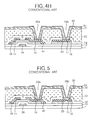
- FIG. 4A to FIG. 4 h shows a method of fabricating the X-ray detecting device shown in FIG. 2 step by step.
- the gate electrode 36 and the gate line 2 are provided on the substrate 1 .
- the gate electrode 36 and the gate line 2 are formed by depositing a metal material using a deposition technique such as a sputtering, etc. to form a conductive layer and then patterning the conductive layer.
- the gate electrode 36 and the gate line 2 are formed from a metal material such as an aluminum ally, and are preferably formed from aluminum-neodymium/molybdenum (AlNd/Mo).
- an active layer 14 and an ohmic contact layer 16 are provided on a gate insulating film 12 .
- the gate insulating film 12 is formed by entirely depositing an insulating material, such as silicon nitride (SiN x ) or silicon oxide (SiO x ), onto the substrate 1 by the plasma enhanced chemical vapor deposition (PECVD) technique in such a manner to cover the gate line 2 and the gate electrode 36 .
- an insulating material such as silicon nitride (SiN x ) or silicon oxide (SiO x .
- the active layer 14 and the ohmic contact layer 16 are formed by sequentially disposing first and second semiconductor material layers 14 and 16 on the gate insulating film 12 and then patterning them.
- the active layer 14 is formed from a first semiconductor material, that is, amorphous silicon that is not doped with an impurity.
- the ohmic contact layer 16 is formed from a second semiconductor material, that is, amorphous silicon doped with an n-type or p-type impurity at a high concentration.
- the data line 42 , the ground electrode 20 , the source electrode 38 and the drain electrode 40 are provided on the gate insulating film 12 .
- the data line 42 , the ground electrode 20 and the source and drain electrodes 38 and 40 are formed by depositing a metal material using the CVD technique or the sputtering technique and then patterning the metal material. After the source and drain electrodes 38 and 40 were patterned, the ohmic contact layer 16 at an area corresponding to the gate electrode 36 also is patterned to expose the active layer 14 . A portion of the active layer 14 exposed by the source and drain electrodes 38 and 40 serves as a channel.
- the data line 42 , the ground electrode 20 , and the source and drain electrodes 38 and 40 are made from chrome (Cr) or molybdenum (Mo).
- a first protective layer 18 are provided on the gate insulating layer 12 .
- the first protective layer 18 is formed by depositing an inorganic insulating material on the gate insulating layer 12 in such a manner to cover the data line 42 , the ground electrode 20 and the source and drain electrodes 38 and 40 and then patterning it.
- the first protective layer 18 is preferably made from silicon nitride (SiN x ) or silicon oxide (SiO x ), etc.
- the first protective layer is provided with a first ground contact hole 24 b and a first drain contact hole 24 a .
- the ground electrode 20 is exposed by the first ground contact hole 24 b passing through the first protective layer 18 .
- the drain electrode 40 is exposed by the first drain contact hole 24 a passing through the first protective layer 18 .
- an organic insulating layer 22 are provided on the first protective layer 18 .
- the organic insulating layer 22 is formed by depositing an organic insulating material, such as an acrylic organic compound, Teflon, BCB (benzocyclobutene), Cytop or PFCB (perfluorocyclobutane), etc., on the first protective layer 18 and then patterning it.
- an organic insulating material such as an acrylic organic compound, Teflon, BCB (benzocyclobutene), Cytop or PFCB (perfluorocyclobutane), etc.
- This organic insulating layer 22 is provided with a second drain contact hole 26 a and a second ground contact hole 26 b .
- Each of the second drain contact hole 26 a and the second ground contact hole 26 b has a width smaller than each of the first drain contact hole 24 a and the first ground contact hole 24 b .
- the drain electrode 40 is exposed by the second drain contact hole 26 a passing through the organic insulating layer 22 .
- the ground electrode 20 is exposed by the second ground contact hole 26 b passing through the organic insulating layer 22 .
- a transparent electrode 30 is provided on the organic insulating layer 22 .
- the transparent electrode 30 is formed by depositing a transparent conductive material onto the organic insulating layer 22 and then patterning the deposited transparent conductive material.
- the transparent electrode 30 is made from a transparent material such as indium-tin-oxide (ITO), indium-zinc-oxide (IZO) or indium-tin-zinc-oxide (ITZO).
- the transparent electrode 30 is electrically connected, via the second drain contact hole 26 a , to the drain electrode 40 while being electrically connected, via the second ground contact hole 26 b , to the ground electrode 20 .
- a second protective layer 32 is provided on the organic insulating layer 22 .
- the second protective layer 32 is formed by depositing an insulating material such as silicon nitride (SiN x ) or silicon oxide (SiO x ) and then patterning it in such a manner to cover the transparent electrode 30 .
- an insulating material such as silicon nitride (SiN x ) or silicon oxide (SiO x )
- the second protective layer 32 is provided with a third drain contact hole 28 a and a third ground contact hole 28 b .
- Each of the third drain contact hole 28 a and the third ground contact hole 28 b has a width smaller than each of the second drain contact hole 26 a and the second ground contact hole 26 b .
- the transparent electrode 30 is exposed by the third drain contact hole 28 a passing through the second protective layer 32 .
- the pixel electrode 34 is provided on the second protective layer 32 .
- the pixel electrode 34 is formed by depositing a transparent conductive material on the second protective layer 32 and then patterning the deposited transparent conductive material.
- the pixel electrode 34 is electrically connected, via the first to third drain contact holes 24 a , 26 a and 28 a , to the drain electrode 40 .
- the pixel electrode 34 is made from a transparent conductive material such as indium-tin-oxide (ITO), indium-zinc-oxide (IZO) or indium-tin-zinc-oxide (ITZO).
- the contact holes 24 a and 24 b are defined to expose the ground electrode 20 and the drain electrode 40 .
- the ground electrode 20 and the drain electrode 40 are electrically connected, via the contact holes 24 a and 24 b , to the transparent electrode 30 .
- the organic insulating material 22 is formed by the photolithography including a dry etching after the ground electrode 20 and the drain electrode 40 were formed from molybdenum (Mo), the ground electrode 20 and the drain electrode 40 also are over-etched to have a difficulty in setting a dry etching condition of the organic insulating layer 22 . This causes a drawback in that only the side surfaces of the over-etched ground and drain electrodes 20 and 40 should be in contact with the transparent electrode 30 , to thereby generate a contact badness.
- Mo molybdenum
- an object of the present invention to provide an X-ray detecting device and a fabricating method thereof that is capable of preventing a contact badness among a drain electrode, a ground electrode and a transparent electrode.
- an X-ray detecting device includes an auxiliary electrode formed on a substrate simultaneously with a gate electrode; a drain electrode electrically connected to the auxiliary electrode; and a transparent electrode electrically connected, via a contact hole passing through the drain electrode, to the auxiliary electrode.
- the X-ray detecting device further includes a gate insulating film formed in such a manner to cover the auxiliary electrode; a semiconductor layer formed in such a manner to correspond to the auxiliary electrode and the gate electrode; and a contact hole passing through the gate insulating film and the semiconductor layer to expose the auxiliary electrode.
- the auxiliary electrode is formed from aluminum-neodymium/molybdenum (AlNd/Mo).
- the drain electrode is formed from molybdenum (Mo).
- the X-ray detecting device further includes an auxiliary electrode formed simultaneously with the gate electrode; a ground electrode electrically connected to the second auxiliary electrode; and a transparent electrode electrically connected, via a contact hole passing through the ground electrode, to the auxiliary electrode.
- the X-ray detecting device further includes a gate insulating film formed on the substrate in such a manner to cover the auxiliary electrode; a semiconductor layer formed on the gate insulating film; and a cont passing through the gate insulating film and the semiconductor layer to expose the auxiliary electrode.
- the auxiliary electrode is formed from aluminum-neodymium/molybdenum (AlNd/Mo).
- the ground electrode is formed from molybdenum (Mo).
- a method of fabricating an X-ray detecting device includes the steps of forming an auxiliary electrode on a substrate simultaneously with a gate electrode; forming a gate insulating film on the substrate in such a manner to cover the gate electrode and the auxiliary electrode; forming a semiconductor layer on the gate insulating film; forming a first contact hole passing through the semiconductor layer and the gate insulating film to expose the auxiliary electrode; and forming a source electrode on the gate insulating film and simultaneously forming a drain electrode opposed to the source electrode and electrically connected to the auxiliary electrode.
- the fabricating method further includes the steps of forming a first protective layer on the gate insulating film in such a manner to cover the source and drain electrode; forming an insulating layer on the first protective layer; forming a second contact hole passing through at least one of the insulating layer and the drain electrode; forming a transparent electrode electrically connected, via the second contact hole, to at least one of the drain electrode and the auxiliary electrode; forming a second protective layer on the insulating layer; and forming a pixel electrode electrically connected to the transparent electrode on the second protective layer.
- the insulating layer is made from an organic insulating material.
- the first and second protective layers are made from an inorganic insulating material.
- the auxiliary electrode is formed from aluminum-neodymium/molybdenum (AlNd/Mo).
- the drain electrode is formed from molybdenum (Mo).
- the fabricating method further includes the steps of forming an auxiliary electrode on the substrate simultaneously with the gate electrode; forming a gate insulating film on the substrate in such a manner to cover the auxiliary electrode; forming a semiconductor layer on the gate insulating film; forming a first contact hole passing through the semiconductor layer and the gate insulating film to expose the auxiliary electrode; and forming a ground electrode electrically connected to the auxiliary electrode on the substrate.
- the fabricating method further includes the steps of forming a first protective layer on the gate insulating film in such a manner to cover the ground electrode; forming an insulating layer on the first protective layer; forming a second contact hole passing through at least one of the insulating layer and the ground electrode; forming a transparent electrode electrically connected, via the second contact hole, to at least one of the ground electrode and the auxiliary electrode; forming a second protective layer on the insulating layer; and forming a pixel electrode on the second protective layer.
- the auxiliary electrode is formed from aluminum-neodymium/molybdenum (AlNd/Mo).
- the ground electrode is formed from molybdenum (Mo).
- the first and second protective layers are made from an inorganic insulating material.
- the insulating layer is made from an organic insulating material.
- FIG. 1 is a schematic block circuit view showing a panel structure of a conventional X-ray detecting device
- FIG. 2 is a plan view showing a structure of the X-ray detecting device shown in FIG. 1;
- FIG. 3 is a section view of the X-ray detecting device taken along the A-A′ line in FIG. 2;
- FIG. 4A to FIG. 4H are section views showing a method of fabricating the X-ray detecting device shown in FIG. 3 step by step;
- FIG. 5 is a section view of the X-ray detecting device for showing an over-etching phenomenon when the ground electrode and the drain electrode are formed from molybdenum;
- FIG. 6 is a plan view showing a structure of an X-ray detecting device according to an embodiment of the present invention.
- FIG. 7 is a section view of the X-ray detecting device taken along the B-B′ line in FIG. 6;
- FIG. 8A to FIG. 8I are plan views showing a method of fabricating the X-ray detecting device in FIG. 6;
- FIG. 9A to FIG. 9I are section views showing a method of fabricating the X-ray detecting device in FIG. 7 .
- FIG. 6 and FIG. 7 there is shown an X-ray detecting device according to an embodiment of the present invention.
- a pixel electrode 84 is formed at a unit pixel area defined by a gate line 52 and a data line 54 .
- a charging capacitor Cst is formed by the pixel electrode 84 and a transparent electrode 80 positioned at the lower portion of the pixel electrode 84 with having an organic insulating layer 82 therebetween.
- a ground electrode 70 is formed in a direction crossing the pixel electrode 84 to reset the residual electric charges of the charging capacitor Cst. The ground electrode 70 is electrically coupled, via a ground contact hole 76 b , to the transparent electrode 80 .
- the thin film transistor is formed at an intersection between the data line 54 and the gate line 52 .
- the TFT consists of a gate electrode 56 extended from the gate line 52 , a source electrode 58 extended from the data line 54 , a drain electrode 60 connected, via drain contact holes 74 a , 76 a and 78 a , to the pixel electrode 84 , and semiconductor layers 64 and 66 for defining a conductive channel between the source electrode 58 and the drain electrode 60 .
- first and second auxiliary electrodes 90 and 92 are formed from aluminum-neodymium/molybdenum (AlNd/Mo) like the gate electrode 56 . Even though the ground electrode 70 and the drain electrode 60 are over-etched simultaneously with a patterning of the organic insulating layer 72 , the first and second auxiliary electrodes 90 and 92 are electrically connected to the transparent electrode 80 .
- FIGS. 8A to 8 I and FIGS. 9A 9 I show a method of fabricating the X-ray detecting device shown in FIG. 6 step by step.
- the gate line 52 , the gate electrode 56 and the first and second auxiliary electrodes 90 and 92 are provided on the substrate 51 .
- the gate line 52 , the gate electrode 56 and the first and second auxiliary electrodes 90 and 92 are formed by depositing a metal material using a deposition technique such as a sputtering, etc. to form a conductive layer and then patterning the conductive layer.
- the first auxiliary electrode 90 is positioned at the lower portion of the drain electrode 60 to be formed later while the second auxiliary electrode 92 is positioned at the lower portion of the ground electrode 70 to be formed later.
- the gate line 52 , the gate electrode 36 and the first and second auxiliary electrodes 90 and 92 are formed from a metal material such as an aluminum ally, and are preferably formed from aluminum-neodymium/molybdenum (AlNd/Mo).
- an active layer 64 and an ohmic contact layer 66 are provided on a gate insulating film 62 .
- the gate insulating film 62 is formed by entirely depositing an insulating material, such as silicon nitride (SiN x ) or silicon oxide (SiO x ), onto the substrate 51 by the plasma enhanced chemical vapor deposition (PECVD) technique in such a manner to cover the gate line 52 , the gate electrode 56 and the first and second auxiliary electrodes 90 and 92 .
- an insulating material such as silicon nitride (SiN x ) or silicon oxide (SiO x .
- the active layer 64 and the ohmic contact layer 66 are formed by sequentially disposing first and second semiconductor materials on the gate insulating film 62 and then patterning them.
- the active layer 64 and the ohmic contact layer 66 at the TFT area are formed in such a manner to correspond to the gate electrode 56 and the first auxiliary electrode 90 .
- the active layer 64 and the ohmic contact layer 66 at the ground area are separately formed with having the second auxiliary electrode 92 therebetween such that the active layer 64 and the ohmic contact layer 66 is not formed on the second auxiliary electrode 92 in order to prevent step coverage between the ground electrode 70 and the transparent electrode 80 to be formed later.
- the active layer 64 is formed from a first semiconductor material, that is, amorphous silicon that is not doped with an impurity.
- the ohmic contact layer 66 is formed from a second semiconductor material, that is, amorphous silicon doped with an n-type or p-type impurity at a high concentration.
- a first ground contact hole 67 b and a first drain contact hole 67 a are formed such that the first and second auxiliary electrodes 90 and 92 on the substrate 51 are exposed.
- a photoresist pattern is formed by coating a photoresist on the gate insulating film 62 and then exposing and developing the photoresist using a desired pattern of mask. Then, the first ground contact hole 67 b and the first drain contact hole 67 a are formed by etching the active layer 64 and the ohmic contact layer 66 using a gas including HCl, etc. in response to the photoresist pattern and thereafter etching the gate insulating film 62 using a gas including SF 6 under this state.
- the data line 54 , the ground electrode 70 , the source electrode 58 and the drain electrode 60 are provided on the gate insulating film 62 .
- the data line 54 , the ground electrode 70 and the source and drain electrodes 58 and 60 are formed by depositing a metal material using the CVD technique or the sputtering technique and then patterning the metal material. After the source and drain electrodes 58 and 60 were patterned, the ohmic contact layer 66 at an area corresponding to the gate electrode 56 also is patterned to expose the active layer 64 . A portion of the active layer 64 exposed by the source and drain electrodes 58 and 60 serves as a channel.
- the drain electrode 60 is electrically coupled to the first auxiliary electrode 90 while the ground electrode 70 is electrically coupled to the second auxiliary electrode 92 .
- the data line 54 , the ground electrode 70 , and the source and drain electrodes 58 and 60 are made from molybdenum (Mo).
- a first protective layer 68 are provided on the gate insulating film 62 .
- the first protective layer 68 is formed by depositing an inorganic insulating material on the gate insulating layer 62 in such a manner to cover the data line 52 , the ground electrode 70 and the source and drain electrodes 58 and 60 and then patterning it.
- the first protective layer 68 is preferably made from silicon nitride (SiN x ) or silicon oxide (SiO x ), etc.
- the first protective layer 68 is provided with a second ground contact hole 74 b and a second drain contact hole 74 a .
- the ground electrode 70 is exposed by the second ground contact hole 74 b passing through the first protective layer 68 .
- the drain electrode 60 is exposed by the second drain contact hole 74 a passing through the first protective film 68 .
- the drain electrode 60 and the ground electrode 70 may be over-etched.
- an organic insulating layer 72 are provided on the first protective layer 68 .
- the organic insulating layer 72 is formed by depositing an organic insulating material, such as an acrylic organic compound, Teflon, BCB (benzocyclobutene), Cytop or PFCB (perfluorocyclobutane), etc., on the first protective layer 18 and then patterning it.
- an organic insulating material such as an acrylic organic compound, Teflon, BCB (benzocyclobutene), Cytop or PFCB (perfluorocyclobutane), etc.
- This organic insulating layer 72 is provided with a third drain contact hole 76 a and a third ground contact hole 76 b .
- Each of the third drain contact hole 76 a and the third ground contact hole 76 b has a width smaller than or equal to each of the second drain contact hole 74 a and the second ground contact hole 74 b.
- the drain electrode 60 is exposed by the third drain contact hole 76 a passing through the organic insulating layer 72 and a portion of the drain electrode 60 .
- the ground electrode 70 is exposed by the third ground contact hole 76 b passing through the organic insulating layer 72 and a portion of the ground electrode 70 .
- the drain electrode 60 may be passed through to expose the first auxiliary electrode 90 through the third drain contact hole 76 a while the ground electrode 70 may be passed through to expose the second auxiliary electrode 92 through the third ground contact hole 76 b.
- a transparent electrode 80 is provided on the organic insulating layer 72 .
- the transparent electrode 80 is formed by depositing a transparent conductive material onto the organic insulating layer 72 and then patterning the deposited transparent conductive material.
- the transparent electrode 70 is made from a transparent material such as indium-tin-oxide (ITO), indium-zinc-oxide (IZO) or indium-tin-zinc-oxide (ITZO).
- the transparent electrode 70 is electrically connected, via the third drain contact hole 76 a , to the drain electrode 60 while being electrically connected, via the third ground contact hole 76 b , to the ground electrode 70 .
- a second protective layer 82 is provided on the organic insulating layer 72 .
- the second protective layer 82 is formed by depositing an insulating material onto the organic insulating layer 72 and then patterning it in such a manner to cover the transparent electrode 80 .
- the second protective layer 82 is provided with a fourth drain contact hole 78 a and a fourth ground contact hole 78 b .
- Each of the fourth drain contact hole 78 a and the fourth ground contact hole 78 b has a width smaller than each of the third drain contact hole 76 a and the third ground contact hole 76 b .
- the transparent electrode 80 is exposed by the fourth drain contact hole 78 a passing through the second protective layer 82 .
- the pixel electrode 84 is provided on the second protective layer 82 .
- the pixel electrode 84 is formed by depositing a transparent conductive material on the second protective layer 82 and then patterning the deposited transparent conductive material.
- the pixel electrode 84 is electrically connected, via the second to fourth drain contact holes 74 a , 76 a and 78 a , to the drain electrode 60 .
- the pixel electrode 84 is made from a transparent conductive material such as indium-tin-oxide (ITO), indium-zinc-oxide (IZO) or indium-tin-zinc-oxide (ITZO).
- the first and second auxiliary electrodes are formed from the same metal material as the gate electrode. Accordingly, the first and second auxiliary electrodes are provided such that the drain electrode and the ground electrode are electrically connected to the transparent electrode with the aid of the first and second auxiliary electrodes even though they are over-etched.
Abstract
Description
Claims (28)
Applications Claiming Priority (2)
| Application Number | Priority Date | Filing Date | Title |
|---|---|---|---|
| KR1020000085278A KR100763137B1 (en) | 2000-12-29 | 2000-12-29 | Fabricating Method of X-ray Detecting Device |
| KRP2000-85278 | 2000-12-29 |
Publications (2)
| Publication Number | Publication Date |
|---|---|
| US20020084419A1 US20020084419A1 (en) | 2002-07-04 |
| US6617584B2 true US6617584B2 (en) | 2003-09-09 |
Family
ID=19703893
Family Applications (1)
| Application Number | Title | Priority Date | Filing Date |
|---|---|---|---|
| US09/888,495 Expired - Lifetime US6617584B2 (en) | 2000-12-29 | 2001-06-26 | X-ray detecting device and fabricating method thereof |
Country Status (2)
| Country | Link |
|---|---|
| US (1) | US6617584B2 (en) |
| KR (1) | KR100763137B1 (en) |
Cited By (5)
| Publication number | Priority date | Publication date | Assignee | Title |
|---|---|---|---|---|
| US20020154234A1 (en) * | 2000-12-29 | 2002-10-24 | Moon Kyo Ho | X-ray detecting device and fabricating method thereof |
| US20030234364A1 (en) * | 2002-06-25 | 2003-12-25 | Hennessy William Andrew | Imaging array and method for manufacturing same |
| US20050258425A1 (en) * | 2002-07-11 | 2005-11-24 | Yoshihiro Izumi | Photoelectric conversion device, image scanning apparatus, and manufacturing method of the photoelectric conversion device |
| US20140339568A1 (en) * | 2013-05-16 | 2014-11-20 | Sumitomo Electric Industries, Ltd. | Semiconductor device with substrate via hole and method to form the same |
| US20210175364A1 (en) * | 2019-12-05 | 2021-06-10 | Lg Display Co., Ltd. | Thin Film Transistor Array Substrate for Digital X-Ray Detector Device, Digital X-Ray Detector Device, and Manufacturing Method Thereof |
Families Citing this family (11)
| Publication number | Priority date | Publication date | Assignee | Title |
|---|---|---|---|---|
| KR100751185B1 (en) * | 2000-08-08 | 2007-08-22 | 엘지.필립스 엘시디 주식회사 | Liquid Crystal Display Device And Method for Fabricating the same |
| SG143063A1 (en) * | 2002-01-24 | 2008-06-27 | Semiconductor Energy Lab | Light emitting device and method of manufacturing the same |
| EP1343206B1 (en) | 2002-03-07 | 2016-10-26 | Semiconductor Energy Laboratory Co., Ltd. | Light emitting apparatus, electronic apparatus, illuminating device and method of fabricating the light emitting apparatus |
| JP2004265932A (en) * | 2003-02-14 | 2004-09-24 | Canon Inc | Radiation imaging device |
| JP4266656B2 (en) * | 2003-02-14 | 2009-05-20 | キヤノン株式会社 | Solid-state imaging device and radiation imaging device |
| KR100965176B1 (en) * | 2003-04-07 | 2010-06-24 | 삼성전자주식회사 | Array panel for digital x-ray detector and method for manufacturing the same |
| KR101218089B1 (en) * | 2007-12-07 | 2013-01-18 | 엘지디스플레이 주식회사 | Digital x-ray detector and method of fabricating the same |
| KR101894392B1 (en) * | 2011-12-28 | 2018-09-04 | 삼성전자주식회사 | Multi-energy radiation detector and method of manufacturing the same |
| KR101367151B1 (en) * | 2012-11-28 | 2014-02-27 | 한국전기연구원 | X-ray image detector with isolation layer for blocking the leakage current and method of manufacturing this |
| JP6072522B2 (en) * | 2012-11-29 | 2017-02-01 | 三菱電機株式会社 | Liquid crystal display panel and manufacturing method thereof |
| CN111106134B (en) * | 2018-10-29 | 2023-08-08 | 夏普株式会社 | Active matrix substrate and X-ray imaging panel provided with same |
Citations (8)
| Publication number | Priority date | Publication date | Assignee | Title |
|---|---|---|---|---|
| US20010022363A1 (en) * | 2000-03-07 | 2001-09-20 | Hisashi Nagata | Image sensor and method of manufacturing the same |
| US6323490B1 (en) * | 1998-03-20 | 2001-11-27 | Kabushiki Kaisha Toshiba | X-ray semiconductor detector |
| US6326249B1 (en) * | 1997-08-26 | 2001-12-04 | Semiconductor Energy Laboratory Co., Ltd. | Semiconductor device and process for producing same |
| US6403965B1 (en) * | 1999-03-26 | 2002-06-11 | Kabushiki Kaisha Toshiba | X-ray image detector system |
| US20020123176A1 (en) * | 1999-05-18 | 2002-09-05 | Sharp Kabushiki Kaisha | Method for fabricating electric interconnections and interconnection substrate having electric interconnections fabricated by the same method |
| US20020154235A1 (en) * | 2000-12-29 | 2002-10-24 | Kim Ik Soo | X-ray detecting device and fabricating method thereof |
| US6480577B1 (en) * | 1999-04-07 | 2002-11-12 | Sharp Kabushiki Kaisha | Active matrix substrate, method of manufacturing same, and flat-panel image sensor |
| US6507026B2 (en) * | 2000-01-12 | 2003-01-14 | Kabushiki Kaisha Toshiba | Planar X-ray detector |
Family Cites Families (2)
| Publication number | Priority date | Publication date | Assignee | Title |
|---|---|---|---|---|
| KR100521257B1 (en) * | 1998-03-26 | 2006-01-12 | 삼성전자주식회사 | Liquid crystal display device having image adjusting means according to external light amount |
| KR100299535B1 (en) * | 1999-05-28 | 2001-09-22 | 남상희 | Method of Testing X-Ray Detecting Device and Apparatus thereof |
-
2000
- 2000-12-29 KR KR1020000085278A patent/KR100763137B1/en active IP Right Grant
-
2001
- 2001-06-26 US US09/888,495 patent/US6617584B2/en not_active Expired - Lifetime
Patent Citations (8)
| Publication number | Priority date | Publication date | Assignee | Title |
|---|---|---|---|---|
| US6326249B1 (en) * | 1997-08-26 | 2001-12-04 | Semiconductor Energy Laboratory Co., Ltd. | Semiconductor device and process for producing same |
| US6323490B1 (en) * | 1998-03-20 | 2001-11-27 | Kabushiki Kaisha Toshiba | X-ray semiconductor detector |
| US6403965B1 (en) * | 1999-03-26 | 2002-06-11 | Kabushiki Kaisha Toshiba | X-ray image detector system |
| US6480577B1 (en) * | 1999-04-07 | 2002-11-12 | Sharp Kabushiki Kaisha | Active matrix substrate, method of manufacturing same, and flat-panel image sensor |
| US20020123176A1 (en) * | 1999-05-18 | 2002-09-05 | Sharp Kabushiki Kaisha | Method for fabricating electric interconnections and interconnection substrate having electric interconnections fabricated by the same method |
| US6507026B2 (en) * | 2000-01-12 | 2003-01-14 | Kabushiki Kaisha Toshiba | Planar X-ray detector |
| US20010022363A1 (en) * | 2000-03-07 | 2001-09-20 | Hisashi Nagata | Image sensor and method of manufacturing the same |
| US20020154235A1 (en) * | 2000-12-29 | 2002-10-24 | Kim Ik Soo | X-ray detecting device and fabricating method thereof |
Cited By (8)
| Publication number | Priority date | Publication date | Assignee | Title |
|---|---|---|---|---|
| US20020154234A1 (en) * | 2000-12-29 | 2002-10-24 | Moon Kyo Ho | X-ray detecting device and fabricating method thereof |
| US7368315B2 (en) * | 2000-12-29 | 2008-05-06 | Lg.Philips Lcd Co., Ltd. | X-ray detecting device and fabricating method thereof |
| US20030234364A1 (en) * | 2002-06-25 | 2003-12-25 | Hennessy William Andrew | Imaging array and method for manufacturing same |
| US6784434B2 (en) * | 2002-06-25 | 2004-08-31 | General Electric Company | Imaging array and method for manufacturing same |
| US20050258425A1 (en) * | 2002-07-11 | 2005-11-24 | Yoshihiro Izumi | Photoelectric conversion device, image scanning apparatus, and manufacturing method of the photoelectric conversion device |
| US20140339568A1 (en) * | 2013-05-16 | 2014-11-20 | Sumitomo Electric Industries, Ltd. | Semiconductor device with substrate via hole and method to form the same |
| US20210175364A1 (en) * | 2019-12-05 | 2021-06-10 | Lg Display Co., Ltd. | Thin Film Transistor Array Substrate for Digital X-Ray Detector Device, Digital X-Ray Detector Device, and Manufacturing Method Thereof |
| US11757046B2 (en) * | 2019-12-05 | 2023-09-12 | Lg Display Co., Ltd. | Thin film transistor array substrate for digital x-ray detector device, digital x-ray detector device, and manufacturing method thereof |
Also Published As
| Publication number | Publication date |
|---|---|
| KR20020055998A (en) | 2002-07-10 |
| KR100763137B1 (en) | 2007-10-02 |
| US20020084419A1 (en) | 2002-07-04 |
Similar Documents
| Publication | Publication Date | Title |
|---|---|---|
| US6423973B2 (en) | X-ray image sensor and method for fabricating the same | |
| US6617584B2 (en) | X-ray detecting device and fabricating method thereof | |
| US6225212B1 (en) | Corrosion resistant imager | |
| US6607935B2 (en) | Method for fabricating array substrate for X-ray detector | |
| US6797961B2 (en) | X-ray detector and method of fabricating the same | |
| JP2009271524A (en) | Image display system and fabrication method thereof | |
| US6528819B2 (en) | Method of fabricating an array substrate for an x-ray detector | |
| KR20010020032A (en) | Fabricating Method of Thin Film Transistor Substrate For Detecting X-ray | |
| US6570161B2 (en) | X-ray detecting device and fabricating method thereof | |
| US7402810B2 (en) | X-ray detecting device and fabricating method thereof | |
| KR100641732B1 (en) | Fabricating Method of X-ray Detecting Device | |
| US7368315B2 (en) | X-ray detecting device and fabricating method thereof | |
| EP0890190B1 (en) | Corrosion resistant imager | |
| KR100730064B1 (en) | Fabricating Method of Thin Film Transistor Substrate For Detecting X-ray | |
| KR20030055504A (en) | a method for manufacturing of digital X-ray detector using TFT | |
| KR100698238B1 (en) | Detecting X-ray Device And Method of Fabricating The Same | |
| KR20010081580A (en) | X-ray image sensor and a method for fabricating the same | |
| KR20040041253A (en) | A X-ray detector and a method for fabricating thereof | |
| KR20030055502A (en) | a method for manufacturing of X-ray detector using TFT array | |
| KR20040054131A (en) | A X-ray detector and a method for fabricating thereof | |
| KR20040013498A (en) | Digital X-ray detector and fabricating method thereof |
Legal Events
| Date | Code | Title | Description |
|---|---|---|---|
| AS | Assignment |
Owner name: L.G. PHILIPS LCD CO., LTD., KOREA, REPUBLIC OF Free format text: ASSIGNMENT OF ASSIGNORS INTEREST;ASSIGNORS:CHOO, KYO SEOP;PARK, JUNE HO;REEL/FRAME:011936/0963 Effective date: 20010614 |
|
| STCF | Information on status: patent grant |
Free format text: PATENTED CASE |
|
| FEPP | Fee payment procedure |
Free format text: PAYOR NUMBER ASSIGNED (ORIGINAL EVENT CODE: ASPN); ENTITY STATUS OF PATENT OWNER: LARGE ENTITY |
|
| FPAY | Fee payment |
Year of fee payment: 4 |
|
| AS | Assignment |
Owner name: LG DISPLAY CO., LTD., KOREA, REPUBLIC OF Free format text: CHANGE OF NAME;ASSIGNOR:LG.PHILIPS LCD CO., LTD.;REEL/FRAME:020985/0675 Effective date: 20080304 Owner name: LG DISPLAY CO., LTD.,KOREA, REPUBLIC OF Free format text: CHANGE OF NAME;ASSIGNOR:LG.PHILIPS LCD CO., LTD.;REEL/FRAME:020985/0675 Effective date: 20080304 |
|
| FEPP | Fee payment procedure |
Free format text: PAYER NUMBER DE-ASSIGNED (ORIGINAL EVENT CODE: RMPN); ENTITY STATUS OF PATENT OWNER: LARGE ENTITY Free format text: PAYOR NUMBER ASSIGNED (ORIGINAL EVENT CODE: ASPN); ENTITY STATUS OF PATENT OWNER: LARGE ENTITY |
|
| FPAY | Fee payment |
Year of fee payment: 8 |
|
| FPAY | Fee payment |
Year of fee payment: 12 |