US6612496B1 - Scan module - Google Patents
Scan module Download PDFInfo
- Publication number
- US6612496B1 US6612496B1 US09/526,839 US52683900A US6612496B1 US 6612496 B1 US6612496 B1 US 6612496B1 US 52683900 A US52683900 A US 52683900A US 6612496 B1 US6612496 B1 US 6612496B1
- Authority
- US
- United States
- Prior art keywords
- photodetector
- module according
- scan module
- scan
- optics
- Prior art date
- Legal status (The legal status is an assumption and is not a legal conclusion. Google has not performed a legal analysis and makes no representation as to the accuracy of the status listed.)
- Expired - Lifetime
Links
Images


Classifications
-
- G—PHYSICS
- G06—COMPUTING; CALCULATING OR COUNTING
- G06K—GRAPHICAL DATA READING; PRESENTATION OF DATA; RECORD CARRIERS; HANDLING RECORD CARRIERS
- G06K7/00—Methods or arrangements for sensing record carriers, e.g. for reading patterns
- G06K7/10—Methods or arrangements for sensing record carriers, e.g. for reading patterns by electromagnetic radiation, e.g. optical sensing; by corpuscular radiation
- G06K7/10544—Methods or arrangements for sensing record carriers, e.g. for reading patterns by electromagnetic radiation, e.g. optical sensing; by corpuscular radiation by scanning of the records by radiation in the optical part of the electromagnetic spectrum
- G06K7/10821—Methods or arrangements for sensing record carriers, e.g. for reading patterns by electromagnetic radiation, e.g. optical sensing; by corpuscular radiation by scanning of the records by radiation in the optical part of the electromagnetic spectrum further details of bar or optical code scanning devices
- G06K7/1098—Methods or arrangements for sensing record carriers, e.g. for reading patterns by electromagnetic radiation, e.g. optical sensing; by corpuscular radiation by scanning of the records by radiation in the optical part of the electromagnetic spectrum further details of bar or optical code scanning devices the scanning arrangement having a modular construction
-
- G—PHYSICS
- G06—COMPUTING; CALCULATING OR COUNTING
- G06K—GRAPHICAL DATA READING; PRESENTATION OF DATA; RECORD CARRIERS; HANDLING RECORD CARRIERS
- G06K17/00—Methods or arrangements for effecting co-operative working between equipments covered by two or more of main groups G06K1/00 - G06K15/00, e.g. automatic card files incorporating conveying and reading operations
- G06K17/0022—Methods or arrangements for effecting co-operative working between equipments covered by two or more of main groups G06K1/00 - G06K15/00, e.g. automatic card files incorporating conveying and reading operations arrangements or provisious for transferring data to distant stations, e.g. from a sensing device
-
- G—PHYSICS
- G06—COMPUTING; CALCULATING OR COUNTING
- G06K—GRAPHICAL DATA READING; PRESENTATION OF DATA; RECORD CARRIERS; HANDLING RECORD CARRIERS
- G06K7/00—Methods or arrangements for sensing record carriers, e.g. for reading patterns
- G06K7/10—Methods or arrangements for sensing record carriers, e.g. for reading patterns by electromagnetic radiation, e.g. optical sensing; by corpuscular radiation
- G06K7/10544—Methods or arrangements for sensing record carriers, e.g. for reading patterns by electromagnetic radiation, e.g. optical sensing; by corpuscular radiation by scanning of the records by radiation in the optical part of the electromagnetic spectrum
- G06K7/10712—Fixed beam scanning
- G06K7/10762—Relative movement
- G06K7/10772—Moved readers, e.g. pen, wand
-
- G—PHYSICS
- G06—COMPUTING; CALCULATING OR COUNTING
- G06K—GRAPHICAL DATA READING; PRESENTATION OF DATA; RECORD CARRIERS; HANDLING RECORD CARRIERS
- G06K7/00—Methods or arrangements for sensing record carriers, e.g. for reading patterns
- G06K7/10—Methods or arrangements for sensing record carriers, e.g. for reading patterns by electromagnetic radiation, e.g. optical sensing; by corpuscular radiation
- G06K7/10544—Methods or arrangements for sensing record carriers, e.g. for reading patterns by electromagnetic radiation, e.g. optical sensing; by corpuscular radiation by scanning of the records by radiation in the optical part of the electromagnetic spectrum
- G06K7/10792—Special measures in relation to the object to be scanned
- G06K7/10801—Multidistance reading
Definitions
- the present invention relates to the field of beam scanning, and in particular, to the use of scan modules for scanning and/or reading dataforms such as bar codes.
- a non-retroreflective axial scan module is disclosed in U.S. Pat. No. 5,506,394, the disclosure of which is incorporated herein by reference.
- the scan element used in the non-retroreflective scan module in the '394 patent is a so-called axial scanner, for example, wherein a light source, such as a laser diode, produces a beam directed along an axis and a movable scan element is disposed along the axis and receives the beam to provide a scanning light beam directed generally along the axis. This provides for a scan engine or module having a narrow width.
- Retroreflective and non-retroreflective scan modules are also known wherein the scanning is not axial, but rather a beam from a laser diode is projected in a direction normal to the outgoing scanning beam prior to being applied to a movable scanning element.
- the non-retroreflective scan module disclosed in the '394 patent has a number of disadvantages, in particular, the photodetector therein is not capable of receiving light reflected from a bar code without also receiving a considerable amount of noise caused by ambient light.
- One object of the present invention is to provide an improvement in an axial non-retroreflective scan module wherein optics are provided to restrict the field of view of the photodetector to the vicinity of a scan line formed by the scan element.
- a non-imaging collector such as the one disclosed in U.S. Pat. No. 5,778,133 increases signal, but unlike an imaging system, it does nothing to decrease the field of view. In fact, non-imaging collectors are generally used where large fields of view are desired. They are therefore a poor choice for a single line scanner.
- the collection system of the present invention increases signal and reduces field of view.
- Another object of the present invention is to provide a pen scanner which comprises a pen housing with a writing element at one end and a non-retroreflective scan module mounted in the pen housing to emit the scanning light beam from the other end.
- the pen scanner is preferably self-contained and has a power source in the pen housing which can comprise a rechargeable or replaceable battery, power management circuitry, signal processing and decoding circuitry and communications circuitry to output data from the device.
- the communications circuitry is preferably wireless and can use the laser light source itself, a radio frequency transmitter or a light emitting diode.
- a further object of the present invention is to utilize the non-retroreflective scan-module in a keychain scanner or a pendant scanner configuration.
- a still further object of the present invention is to provide a scan module of either the non-retroreflective or retroreflective type and of either the axial and non-axial type, wherein the housing thereof comprises a block mounting a light source, scan element, photodetector and optics and wherein the block is mountable on a printed circuit board having signal processing and decoding circuitry thereon to output a signal from the photodetector to the signal processing and decoding circuitry.
- the photodetector. can be mounted on the motherboard, with the block carrying the optical filter and photodiode aperture.
- the block carries the laser with its focusing optics, the scan motor and the collection optics (if used). It can also carry the optical filter for the. photodiode and an aperture that the photodiode receives light through.
- the block retains all optical components in proper alignment.
- the printed circuit board may be a motherboard for another device which utilizes a scanning input.
- the motherboard can be.a printed circuit board for a personal digital assistant, a cell phone or any other electronic device which may also require a scanning capability.
- the circuitry for the scan module is already provided on the circuit board and one need only mount the block with the aforesaid scanner elements thereon to scan and decode bar codes and the like.
- Another object of the present invention is to provide a mounting assembly for a non-retroreflective scan module, so that it can be easily and removeably mounted in a device housing or the like.
- Still another object of the present invention is to provide an improvement in an axial non-retroreflective scan module wherein the laser is pulsed at a frequency to enable the electronics to distinguish between signal and noise.
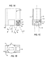
- FIGS. 1A-1C are top, front and side views of a scan module according to the present invention.
- FIGS. 2A-2C are side, front and top views of another embodiment of a scan module according to the present invention.
- FIGS. 3A-3C are side, front and top views of a further embodiment of a scan module according to the present invention.
- FIGS. 4A-4C are side, front and top views of still another embodiment of the scan module according to the present invention.
- FIG. 5 is a pen scanner according to the present invention.
- FIG. 6 is an illustration of another embodiment of a scan module in accordance with the present invention.
- FIGS. 7A-7C illustrate optical AGC according to the present invention.
- a laser focus and scan mirror drive assembly 13 is disposed between two printed circuit boards 11 and 12 .
- the laser focus and scan-mirror drive assembly is the axial non-retroreflective assembly disclosed, for example, in U.S. Pat. No. 5,506,394. The assembly produces a beam along axis A which is then scanned through a window 18 between lines S—S, as shown in FIG. 1 A.
- a photodetector 14 In order to detect light reflected from a dataform, such as a bar code, a photodetector 14 is provided. In order to restrict the field of view F—F of the photodetector, a collection lens 16 is disposed along one side of the module and the photodetector is recessed back behind the collection lens as shown. Disposed between the lens 16 and the photodetector 14 is a filter 15 for filtering out wavelengths other than those of the laser diode in assembly 13 and optionally, a slit aperture 17 which is configured to be long and narrow and aligned with the image of the scan line on a dataform as imaged by lens 16 onto photodetector 14 .
- the filter can be between the lens and symbol if desired, but it will be larger and more expensive.
- the slit size is dependent upon the geometry of the system. In this way, the field of view of the photodetector 14 is limited to the vicinity of the scan line on the bar code and the photodetector can
- the photodetector 14 such as a photodiode, itself can be long and thin and thereby have a width matching the scan line image, as is shown in FIG. 1 C.
- the photodiode surface size is also dictated by the geometry of the system.
- the slit aperture is optional.
- FIGS. 1A-1C illustrate the photodiode and lens on one side of the assembly 13 , it can also be mounted on the other side or above or below the assembly 13 .
- two photodiodes can be used with one on either side of the assembly or above and below the assembly If the lens and detector are above or below the plane of the scanned laser the images on the detector will move up and down on the detector as the symbol is moved closer or further away, due to parallax. In this case, the photodiode aperture has to be enlarged in the vertical direction, or the laser will be out of view at some distances. Enlarging the aperture (or shape of the photodiode) increases field of view, decreasing ambient light immunity. This is still better than a bare photodiode.
- FIGS. 2A-2C illustrate another embodiment 10 B of the present invention wherein the photodetector 14 is disposed so that its surface is parallel to the scan axis A and to the plane of the scan beam and it is disposed between the assembly 13 and window 18 ′ as shown.
- a reflector 20 is disposed behind the window 18 ′ and it is preferably a parabolic reflector, although it can also be a spherical elliptical or cylindrical reflector.
- the photodetector or photodiode 14 is configured to limit the field of view to the vicinity of the scan line as imaged by the reflector 20 thereon.
- This embodiment is more compact than that of FIGS. 1A-1C, since all of the scanning elements are enclosed in the housing of the assembly 13 .
- the reflector 20 and the photodiode 14 can be disposed on the side of assembly 13 or above or below assembly 13 , as in scan module 10 A.
- FIGS. 3A-3C illustrate a further embodiment of the present invention.
- the photodiode 14 and filter 15 are mounted on a PC board 22 installed in front of the assembly 13 .
- the plane of the photodiode is parallel to the axis A and thus a fold mirror 20 ′ is provided to direct light reflected from a bar code.
- a fresnel collection lens 21 is provided, which is preferably part of window 18 ′, but which can be separate therefrom.
- the lens can also be spherical or cylindrical, or it can be a conventional (non-fresnel) lens.
- FIGS. 4A-4C illustrate a still further embodiment 10 D of the invention.
- the photodiode is again in front of the assembly 13 , however the photodiode is facing in the axial direction A and has the filter 15 therewith and is mounted on a board 22 ′.
- the collection lens 23 is preferably spherical or cylindrical and is part of window 24 , although it could also be separate therefrom.
- the photodiode has a width.to match the scan line image formed by the collection lens 23 .
- This embodiment is more compact than that of FIGS. 1A-1C, since all of the scanning elements are enclosed in the housing of the assembly 13 .
- the reflector 20 and the photodiode 14 can be disposed on the side of assembly 13 or above or below assembly 13 , as in scan module 10 A.
- ambient light can be distinguished from signal by pulsing the laser beam produced by the laser diode.
- the beam is pulsed at a frequency preferably greater than 5 times the highest frequency of the baseband signal.
- the typical highest frequency of a baseband signal is approximately 30 kHz so that the beam is pulsed out at least 150 kHz and preferably about 450 kHz.
- FIG. 5 illustrates an embodiment of the present invention wherein a pen housing 30 has any one of the modules 10 A- 10 D referenced as 10 in FIG. 5, so that the scan lines S—S can be emitted from one end thereof.
- the module 10 includes all of the signal processing and decoding circuitry thereon in one or two or more printed circuit boards forming the housing of the module.
- a writing element 28 which can be a retractable pen cartridge or fixed pen with a cap or the like, and batteries 29 A, 29 B which can be either replaceable or rechargeable AA or AAA batteries.
- communications circuitry 40 Also included in the pen housing 30 is communications circuitry 40 .
- the communications circuitry may be circuitry which controls the laser in the module 10 to emit a pulsed output to indicate data. It can also include an LED which can indicate successful decodes when decoding is being carried out and which can also communicate data via pulsing of the light beam (other optical interfaces such as IRDA can also be used and returning data can be received by scanner photodiode).
- the decode LED can be actuated to transmit data.
- the circuitry 40 can also be a wireless RF transceiver for communicating data to a host or terminal.
- the device also includes power management circuitry 41 which is connected to the other components and saves power by shutting off the scan module after a successful decode or a time-out period and/or by staggering the activation of the various components to reduce peak power draws. For example, the circuitry may first turn on a scan motor and let it come up to full speed before laser turn on. Similarly, laser turn on may be delayed until the circuitry has gone through its initiation routine. This will not only reduce overall power drain on the batteries, but will also minimize current spikes (instantaneous) current draw. This is important with small batteries that have high internal resistance.
- FIG. 6 illustrates another embodiment of the present invention.
- the module 100 can be any one of the scan modules 10 A- 10 D discussed hereinabove, or it can be a retroreflective and/or non-axial scan module.
- the module housing includes a block 110 on which a laser scanner assembly 130 including a laser source and a moveable scan element, as well as photodetector 140 and collecting optics 150 .
- the photodetector 140 generates a signal corresponding to light reflected from a dataform, such as a bar code, and this signal from the scan module is to be signal processed, such as by being amplified and digitized, and is thereafter decoded. This is carried out by signal processing and decoding circuitry.
- the signal processing and decoding circuitry is preferably mounted on a printed circuit board 101 , so that one need only mount the module block 110 to the printed circuit board to connect the output of the photodetector to the circuitry or to direct collected light to the photodiode mounted on the circuit board.
- Other signals for the module for example, a motor drive signal, a motor feedback signal, a laser drive signal and a laser feedback signal, would also be connected.
- the printed circuit board 101 is the motherboard for another device, such as a cellular phone, a personal digital assistant, a computer terminal or the like.
- the motherboard 101 can be constructed with all of the electronics thereon for the scan module, and in order to add the scanning functionality to the device, one need only mount the module block with its supported components shown in FIG. 6 to the motherboard and make the connections therebetween.
- Power management circuitry and communications circuitry can also be mounted on the motherboard to give additional functionality to the scan module.
- the modules 10 A- 10 D can be mounted in housings in a simple manner by the-use of a two screw mount disclosed in U.S. application Ser. No. 09/275,858, filed May 24, 1999, the disclosure of which is incorporated herein by reference.
- optical AGC optical automatic gain control
- FIGS. 7A-7C it is merely necessary to focus the collection system so that the image of the scan line 73 , on the detector 71 through aperture 70 is best when the symbol is far away from the scanner at L 1 , for example, for systems described above, which have a useable range of around two to two and a half feet, the system might be focused about one to two feet out and the detector is positioned near the focal length of the lens L f .
- FIG. 7A is a top view and FIG. 7B is a side view thereof. When a symbol is positioned closer than this, the image on the detector is out of focus, causing a blurry line, instead of a sharply defined line on the detector.
- This optical AGC can be used with a spherical lens 72 or a cylindrical or elliptical lens.
Abstract
Description
Claims (57)
Priority Applications (1)
| Application Number | Priority Date | Filing Date | Title |
|---|---|---|---|
| US09/526,839 US6612496B1 (en) | 2000-03-16 | 2000-03-16 | Scan module |
Applications Claiming Priority (1)
| Application Number | Priority Date | Filing Date | Title |
|---|---|---|---|
| US09/526,839 US6612496B1 (en) | 2000-03-16 | 2000-03-16 | Scan module |
Publications (1)
| Publication Number | Publication Date |
|---|---|
| US6612496B1 true US6612496B1 (en) | 2003-09-02 |
Family
ID=27766383
Family Applications (1)
| Application Number | Title | Priority Date | Filing Date |
|---|---|---|---|
| US09/526,839 Expired - Lifetime US6612496B1 (en) | 2000-03-16 | 2000-03-16 | Scan module |
Country Status (1)
| Country | Link |
|---|---|
| US (1) | US6612496B1 (en) |
Cited By (11)
| Publication number | Priority date | Publication date | Assignee | Title |
|---|---|---|---|---|
| US20050028014A1 (en) * | 2003-08-01 | 2005-02-03 | Allred J. Joseph | Intelligent power management control system and method |
| US20060266839A1 (en) * | 2005-05-31 | 2006-11-30 | Symbol Technologies, Inc. | Retro-reflective scanner having exit window with positive optical power |
| GB2445030A (en) * | 2006-12-22 | 2008-06-25 | Duncan Richard Louttit | Hand-held graphic recognition devices |
| US20110069364A1 (en) * | 2009-09-23 | 2011-03-24 | Metrologic Instruments, Inc. | Scan element for use in scanning light and method of making the same |
| US20110069365A1 (en) * | 2009-09-23 | 2011-03-24 | Metrologic Instruments, Inc. | Scan element for use in scanning light and method of making the same |
| US8002183B2 (en) | 2005-10-20 | 2011-08-23 | Metrologic Instruments, Inc. | Scanner flipper integrity indicator |
| US8390909B2 (en) | 2009-09-23 | 2013-03-05 | Metrologic Instruments, Inc. | Molded elastomeric flexural elements for use in a laser scanning assemblies and scanners, and methods of manufacturing, tuning and adjusting the same |
| US8746563B2 (en) | 2012-06-10 | 2014-06-10 | Metrologic Instruments, Inc. | Laser scanning module with rotatably adjustable laser scanning assembly |
| US8915439B2 (en) | 2012-02-06 | 2014-12-23 | Metrologic Instruments, Inc. | Laser scanning modules embodying silicone scan element with torsional hinges |
| USD734752S1 (en) * | 2014-11-18 | 2015-07-21 | Foxlink Image Technology Co., Ltd. | Wireless scanner |
| USD741330S1 (en) * | 2014-11-18 | 2015-10-20 | Foxlink Image Technology Co., Ltd. | Wireless scanner |
Citations (15)
| Publication number | Priority date | Publication date | Assignee | Title |
|---|---|---|---|---|
| US4570057A (en) * | 1981-12-28 | 1986-02-11 | Norand Corporation | Instant portable bar code reader |
| US5367151A (en) | 1989-10-30 | 1994-11-22 | Symbol Technologies, Inc. | Slim scan module with interchangeable scan element |
| US5479000A (en) | 1989-10-30 | 1995-12-26 | Symbol Technologies, Inc. | Compact scanning module for reading bar codes |
| US5506394A (en) | 1990-11-15 | 1996-04-09 | Gap Technologies, Inc. | Light beam scanning pen, scan module for the device and method of utilization |
| US5581067A (en) | 1990-05-08 | 1996-12-03 | Symbol Technologies, Inc. | Compact bar code scanning module with shock protection |
| US5581068A (en) * | 1982-01-25 | 1996-12-03 | Symbol Technologies, Inc. | System for reading coded indica with increased depth of field |
| US5629510A (en) | 1992-12-04 | 1997-05-13 | Psc Inc. | Bar code scanning and reading apparatus with an oscillating scanning engine |
| US5693929A (en) | 1989-10-30 | 1997-12-02 | Symbol Technologies, Inc. | Scanning module with spring made resistant to overflexing |
| WO1998012660A1 (en) | 1996-09-23 | 1998-03-26 | Psc Scanning, Inc. | Dithering assemblies for barcode scanners |
| US5747823A (en) * | 1995-08-08 | 1998-05-05 | Hitachi Maxell, Ltd. | Two-dimensional code mark detecting method and apparatus therefor |
| US5778133A (en) | 1994-04-29 | 1998-07-07 | Geo Labs, Inc. | Nonimaging light collector |
| US5874720A (en) | 1989-10-30 | 1999-02-23 | Symbol Technologies, Inc. | Electro-magnetically activated scanner with suspended scanner component |
| US5988502A (en) * | 1995-03-17 | 1999-11-23 | Symbol Technologies, Inc. | Electro-optical scanner having selectable scan pattern |
| US6112992A (en) * | 1998-06-17 | 2000-09-05 | Motorola, Inc. | Optical code reader and methods and articles therefor |
| US6415981B1 (en) * | 1998-11-26 | 2002-07-09 | Denso Corporation | Optical reader with reduced-sized optical sensor configuration |
-
2000
- 2000-03-16 US US09/526,839 patent/US6612496B1/en not_active Expired - Lifetime
Patent Citations (16)
| Publication number | Priority date | Publication date | Assignee | Title |
|---|---|---|---|---|
| US4570057A (en) * | 1981-12-28 | 1986-02-11 | Norand Corporation | Instant portable bar code reader |
| US5581068A (en) * | 1982-01-25 | 1996-12-03 | Symbol Technologies, Inc. | System for reading coded indica with increased depth of field |
| US5693929A (en) | 1989-10-30 | 1997-12-02 | Symbol Technologies, Inc. | Scanning module with spring made resistant to overflexing |
| US5367151A (en) | 1989-10-30 | 1994-11-22 | Symbol Technologies, Inc. | Slim scan module with interchangeable scan element |
| US5479000A (en) | 1989-10-30 | 1995-12-26 | Symbol Technologies, Inc. | Compact scanning module for reading bar codes |
| US5874720A (en) | 1989-10-30 | 1999-02-23 | Symbol Technologies, Inc. | Electro-magnetically activated scanner with suspended scanner component |
| US5581067A (en) | 1990-05-08 | 1996-12-03 | Symbol Technologies, Inc. | Compact bar code scanning module with shock protection |
| US5763863A (en) | 1990-05-08 | 1998-06-09 | Symbol Technologies, Inc. | Compact bar code scanning module with folded beam path and reflector mounted on spring |
| US5506394A (en) | 1990-11-15 | 1996-04-09 | Gap Technologies, Inc. | Light beam scanning pen, scan module for the device and method of utilization |
| US5629510A (en) | 1992-12-04 | 1997-05-13 | Psc Inc. | Bar code scanning and reading apparatus with an oscillating scanning engine |
| US5778133A (en) | 1994-04-29 | 1998-07-07 | Geo Labs, Inc. | Nonimaging light collector |
| US5988502A (en) * | 1995-03-17 | 1999-11-23 | Symbol Technologies, Inc. | Electro-optical scanner having selectable scan pattern |
| US5747823A (en) * | 1995-08-08 | 1998-05-05 | Hitachi Maxell, Ltd. | Two-dimensional code mark detecting method and apparatus therefor |
| WO1998012660A1 (en) | 1996-09-23 | 1998-03-26 | Psc Scanning, Inc. | Dithering assemblies for barcode scanners |
| US6112992A (en) * | 1998-06-17 | 2000-09-05 | Motorola, Inc. | Optical code reader and methods and articles therefor |
| US6415981B1 (en) * | 1998-11-26 | 2002-07-09 | Denso Corporation | Optical reader with reduced-sized optical sensor configuration |
Non-Patent Citations (2)
| Title |
|---|
| Symbol-SE-900-100A Scan Engine Integration Guide-Revision A-Apr. 1998. |
| Symbol—SE-900-100A Scan Engine Integration Guide—Revision A—Apr. 1998. |
Cited By (17)
| Publication number | Priority date | Publication date | Assignee | Title |
|---|---|---|---|---|
| US7360100B2 (en) * | 2003-08-01 | 2008-04-15 | Ge Medical Systems Global Technology Company, Llc | Intelligent power management control system and method |
| US20050028014A1 (en) * | 2003-08-01 | 2005-02-03 | Allred J. Joseph | Intelligent power management control system and method |
| US20060266839A1 (en) * | 2005-05-31 | 2006-11-30 | Symbol Technologies, Inc. | Retro-reflective scanner having exit window with positive optical power |
| US7204424B2 (en) * | 2005-05-31 | 2007-04-17 | Symbol Technologies, Inc. | Retro-reflective scanner having exit window with positive optical power |
| US8002183B2 (en) | 2005-10-20 | 2011-08-23 | Metrologic Instruments, Inc. | Scanner flipper integrity indicator |
| GB2445030A (en) * | 2006-12-22 | 2008-06-25 | Duncan Richard Louttit | Hand-held graphic recognition devices |
| GB2445030B (en) * | 2006-12-22 | 2009-06-17 | Duncan Richard Louttit | Improvements in graphic recognition devices |
| US20110069364A1 (en) * | 2009-09-23 | 2011-03-24 | Metrologic Instruments, Inc. | Scan element for use in scanning light and method of making the same |
| US20110069365A1 (en) * | 2009-09-23 | 2011-03-24 | Metrologic Instruments, Inc. | Scan element for use in scanning light and method of making the same |
| US8059324B2 (en) | 2009-09-23 | 2011-11-15 | Metrologic Instruments, Inc. | Scan element for use in scanning light and method of making the same |
| US8294969B2 (en) | 2009-09-23 | 2012-10-23 | Metrologic Instruments, Inc. | Scan element for use in scanning light and method of making the same |
| US8390909B2 (en) | 2009-09-23 | 2013-03-05 | Metrologic Instruments, Inc. | Molded elastomeric flexural elements for use in a laser scanning assemblies and scanners, and methods of manufacturing, tuning and adjusting the same |
| US8915439B2 (en) | 2012-02-06 | 2014-12-23 | Metrologic Instruments, Inc. | Laser scanning modules embodying silicone scan element with torsional hinges |
| US9158951B2 (en) | 2012-02-06 | 2015-10-13 | Metrologic Instruments, Inc. | Laser scanning modules embodying silicone scan element with torsional hinges |
| US8746563B2 (en) | 2012-06-10 | 2014-06-10 | Metrologic Instruments, Inc. | Laser scanning module with rotatably adjustable laser scanning assembly |
| USD734752S1 (en) * | 2014-11-18 | 2015-07-21 | Foxlink Image Technology Co., Ltd. | Wireless scanner |
| USD741330S1 (en) * | 2014-11-18 | 2015-10-20 | Foxlink Image Technology Co., Ltd. | Wireless scanner |
Similar Documents
| Publication | Publication Date | Title |
|---|---|---|
| JP3056590B2 (en) | Optical scanner with increased depth of focus | |
| US4578571A (en) | Portable bar code scanning device and method | |
| US5357101A (en) | Electro-optical transceiver with nonimaging concentrator | |
| US5475206A (en) | Scanner assembly | |
| EP0433593B1 (en) | Bar code symbol readers with edge enhancement | |
| US5923021A (en) | Light collection systems in electro-optical readers | |
| US6621070B2 (en) | Bar code scanning system with offset optical axes | |
| US6260763B1 (en) | Integral illumination source/collection lens assembly for data reading system | |
| US9495573B2 (en) | Low profile illumination for direct part mark readers | |
| US6612496B1 (en) | Scan module | |
| EP0349770B1 (en) | Optical device for detecting coded symbols | |
| CA2507997C (en) | Image scanning device having a system for determining the distance to a target | |
| USRE36528E (en) | Optical scanning head | |
| CA2170934C (en) | Optical scanners having dual surface optical elements for dual working ranges | |
| EP1039409A2 (en) | Retro-reflective scan module for electro-optical readers | |
| CN100483441C (en) | Electro-optical reader with improved performance in high intensity ambient light | |
| US7992786B2 (en) | Bar code reader | |
| US5187353A (en) | Bar code symbol scanner utilizing monitor photodiode of laser diode package as a photoreceiver | |
| US5233170A (en) | Bar code symbol scanner utilizing monitor photodiode of laser diode package as a photoreceiver | |
| US6732935B2 (en) | Multipurpose lens holder for reading optically encoded indicia | |
| US6276606B1 (en) | Full range bar code scanner | |
| US7428999B2 (en) | MEMS-based electro-optical reader and method with extended working range | |
| JP2003023202A (en) | Structure of light emitting and light receiving device | |
| KR100347051B1 (en) | A Laser Beam Receiver having Ball Lens in the Laser Transceiver | |
| CN1038536C (en) | Light scanor with enlarged focal length |
Legal Events
| Date | Code | Title | Description |
|---|---|---|---|
| AS | Assignment |
Owner name: SYMBOL TECHNOLOGIES, INC., NEW YORK Free format text: ASSIGNMENT OF ASSIGNORS INTEREST;ASSIGNORS:BARKAN, EDWARD;SHEPARD, HOWARD;REEL/FRAME:010687/0367 Effective date: 20000313 |
|
| STCF | Information on status: patent grant |
Free format text: PATENTED CASE |
|
| AS | Assignment |
Owner name: JPMORGAN CHASE BANK, N.A., NEW YORK Free format text: SECURITY INTEREST;ASSIGNOR:SYMBOL TECHNOLOGIES, INC.;REEL/FRAME:016116/0203 Effective date: 20041229 |
|
| FPAY | Fee payment |
Year of fee payment: 4 |
|
| AS | Assignment |
Owner name: SYMBOL TECHNOLOGIES, INC., NEW YORK Free format text: RELEASE BY SECURED PARTY;ASSIGNOR:JPMORGANCHASE BANK, N.A.;REEL/FRAME:025441/0228 Effective date: 20060901 |
|
| FPAY | Fee payment |
Year of fee payment: 8 |
|
| AS | Assignment |
Owner name: MORGAN STANLEY SENIOR FUNDING, INC. AS THE COLLATERAL AGENT, MARYLAND Free format text: SECURITY AGREEMENT;ASSIGNORS:ZIH CORP.;LASER BAND, LLC;ZEBRA ENTERPRISE SOLUTIONS CORP.;AND OTHERS;REEL/FRAME:034114/0270 Effective date: 20141027 Owner name: MORGAN STANLEY SENIOR FUNDING, INC. AS THE COLLATE Free format text: SECURITY AGREEMENT;ASSIGNORS:ZIH CORP.;LASER BAND, LLC;ZEBRA ENTERPRISE SOLUTIONS CORP.;AND OTHERS;REEL/FRAME:034114/0270 Effective date: 20141027 |
|
| FPAY | Fee payment |
Year of fee payment: 12 |
|
| AS | Assignment |
Owner name: SYMBOL TECHNOLOGIES, LLC, NEW YORK Free format text: CHANGE OF NAME;ASSIGNOR:SYMBOL TECHNOLOGIES, INC.;REEL/FRAME:036083/0640 Effective date: 20150410 |
|
| AS | Assignment |
Owner name: SYMBOL TECHNOLOGIES, INC., NEW YORK Free format text: RELEASE BY SECURED PARTY;ASSIGNOR:MORGAN STANLEY SENIOR FUNDING, INC.;REEL/FRAME:036371/0738 Effective date: 20150721 |