US6501173B2 - Semiconductor device - Google Patents
Semiconductor device Download PDFInfo
- Publication number
- US6501173B2 US6501173B2 US09/797,719 US79771901A US6501173B2 US 6501173 B2 US6501173 B2 US 6501173B2 US 79771901 A US79771901 A US 79771901A US 6501173 B2 US6501173 B2 US 6501173B2
- Authority
- US
- United States
- Prior art keywords
- chip
- memory
- semiconductor
- controller
- external terminals
- Prior art date
- Legal status (The legal status is an assumption and is not a legal conclusion. Google has not performed a legal analysis and makes no representation as to the accuracy of the status listed.)
- Expired - Lifetime
Links
Images


Classifications
-
- H—ELECTRICITY
- H01—ELECTRIC ELEMENTS
- H01L—SEMICONDUCTOR DEVICES NOT COVERED BY CLASS H10
- H01L23/00—Details of semiconductor or other solid state devices
- H01L23/48—Arrangements for conducting electric current to or from the solid state body in operation, e.g. leads, terminal arrangements ; Selection of materials therefor
-
- H—ELECTRICITY
- H01—ELECTRIC ELEMENTS
- H01L—SEMICONDUCTOR DEVICES NOT COVERED BY CLASS H10
- H01L24/00—Arrangements for connecting or disconnecting semiconductor or solid-state bodies; Methods or apparatus related thereto
- H01L24/01—Means for bonding being attached to, or being formed on, the surface to be connected, e.g. chip-to-package, die-attach, "first-level" interconnects; Manufacturing methods related thereto
- H01L24/42—Wire connectors; Manufacturing methods related thereto
- H01L24/47—Structure, shape, material or disposition of the wire connectors after the connecting process
- H01L24/49—Structure, shape, material or disposition of the wire connectors after the connecting process of a plurality of wire connectors
-
- H—ELECTRICITY
- H01—ELECTRIC ELEMENTS
- H01L—SEMICONDUCTOR DEVICES NOT COVERED BY CLASS H10
- H01L23/00—Details of semiconductor or other solid state devices
- H01L23/48—Arrangements for conducting electric current to or from the solid state body in operation, e.g. leads, terminal arrangements ; Selection of materials therefor
- H01L23/488—Arrangements for conducting electric current to or from the solid state body in operation, e.g. leads, terminal arrangements ; Selection of materials therefor consisting of soldered or bonded constructions
- H01L23/495—Lead-frames or other flat leads
- H01L23/49575—Assemblies of semiconductor devices on lead frames
-
- H—ELECTRICITY
- H01—ELECTRIC ELEMENTS
- H01L—SEMICONDUCTOR DEVICES NOT COVERED BY CLASS H10
- H01L23/00—Details of semiconductor or other solid state devices
- H01L23/48—Arrangements for conducting electric current to or from the solid state body in operation, e.g. leads, terminal arrangements ; Selection of materials therefor
- H01L23/50—Arrangements for conducting electric current to or from the solid state body in operation, e.g. leads, terminal arrangements ; Selection of materials therefor for integrated circuit devices, e.g. power bus, number of leads
-
- H—ELECTRICITY
- H01—ELECTRIC ELEMENTS
- H01L—SEMICONDUCTOR DEVICES NOT COVERED BY CLASS H10
- H01L25/00—Assemblies consisting of a plurality of individual semiconductor or other solid state devices ; Multistep manufacturing processes thereof
- H01L25/18—Assemblies consisting of a plurality of individual semiconductor or other solid state devices ; Multistep manufacturing processes thereof the devices being of types provided for in two or more different subgroups of the same main group of groups H01L27/00 - H01L33/00, or in a single subclass of H10K, H10N
-
- H—ELECTRICITY
- H01—ELECTRIC ELEMENTS
- H01L—SEMICONDUCTOR DEVICES NOT COVERED BY CLASS H10
- H01L2224/00—Indexing scheme for arrangements for connecting or disconnecting semiconductor or solid-state bodies and methods related thereto as covered by H01L24/00
- H01L2224/01—Means for bonding being attached to, or being formed on, the surface to be connected, e.g. chip-to-package, die-attach, "first-level" interconnects; Manufacturing methods related thereto
- H01L2224/02—Bonding areas; Manufacturing methods related thereto
- H01L2224/04—Structure, shape, material or disposition of the bonding areas prior to the connecting process
- H01L2224/05—Structure, shape, material or disposition of the bonding areas prior to the connecting process of an individual bonding area
- H01L2224/0554—External layer
- H01L2224/0555—Shape
- H01L2224/05552—Shape in top view
- H01L2224/05554—Shape in top view being square
-
- H—ELECTRICITY
- H01—ELECTRIC ELEMENTS
- H01L—SEMICONDUCTOR DEVICES NOT COVERED BY CLASS H10
- H01L2224/00—Indexing scheme for arrangements for connecting or disconnecting semiconductor or solid-state bodies and methods related thereto as covered by H01L24/00
- H01L2224/01—Means for bonding being attached to, or being formed on, the surface to be connected, e.g. chip-to-package, die-attach, "first-level" interconnects; Manufacturing methods related thereto
- H01L2224/10—Bump connectors; Manufacturing methods related thereto
- H01L2224/15—Structure, shape, material or disposition of the bump connectors after the connecting process
- H01L2224/16—Structure, shape, material or disposition of the bump connectors after the connecting process of an individual bump connector
-
- H—ELECTRICITY
- H01—ELECTRIC ELEMENTS
- H01L—SEMICONDUCTOR DEVICES NOT COVERED BY CLASS H10
- H01L2224/00—Indexing scheme for arrangements for connecting or disconnecting semiconductor or solid-state bodies and methods related thereto as covered by H01L24/00
- H01L2224/01—Means for bonding being attached to, or being formed on, the surface to be connected, e.g. chip-to-package, die-attach, "first-level" interconnects; Manufacturing methods related thereto
- H01L2224/26—Layer connectors, e.g. plate connectors, solder or adhesive layers; Manufacturing methods related thereto
- H01L2224/31—Structure, shape, material or disposition of the layer connectors after the connecting process
- H01L2224/32—Structure, shape, material or disposition of the layer connectors after the connecting process of an individual layer connector
- H01L2224/321—Disposition
- H01L2224/32135—Disposition the layer connector connecting between different semiconductor or solid-state bodies, i.e. chip-to-chip
- H01L2224/32145—Disposition the layer connector connecting between different semiconductor or solid-state bodies, i.e. chip-to-chip the bodies being stacked
-
- H—ELECTRICITY
- H01—ELECTRIC ELEMENTS
- H01L—SEMICONDUCTOR DEVICES NOT COVERED BY CLASS H10
- H01L2224/00—Indexing scheme for arrangements for connecting or disconnecting semiconductor or solid-state bodies and methods related thereto as covered by H01L24/00
- H01L2224/01—Means for bonding being attached to, or being formed on, the surface to be connected, e.g. chip-to-package, die-attach, "first-level" interconnects; Manufacturing methods related thereto
- H01L2224/26—Layer connectors, e.g. plate connectors, solder or adhesive layers; Manufacturing methods related thereto
- H01L2224/31—Structure, shape, material or disposition of the layer connectors after the connecting process
- H01L2224/32—Structure, shape, material or disposition of the layer connectors after the connecting process of an individual layer connector
- H01L2224/321—Disposition
- H01L2224/32151—Disposition the layer connector connecting between a semiconductor or solid-state body and an item not being a semiconductor or solid-state body, e.g. chip-to-substrate, chip-to-passive
- H01L2224/32221—Disposition the layer connector connecting between a semiconductor or solid-state body and an item not being a semiconductor or solid-state body, e.g. chip-to-substrate, chip-to-passive the body and the item being stacked
- H01L2224/32225—Disposition the layer connector connecting between a semiconductor or solid-state body and an item not being a semiconductor or solid-state body, e.g. chip-to-substrate, chip-to-passive the body and the item being stacked the item being non-metallic, e.g. insulating substrate with or without metallisation
-
- H—ELECTRICITY
- H01—ELECTRIC ELEMENTS
- H01L—SEMICONDUCTOR DEVICES NOT COVERED BY CLASS H10
- H01L2224/00—Indexing scheme for arrangements for connecting or disconnecting semiconductor or solid-state bodies and methods related thereto as covered by H01L24/00
- H01L2224/01—Means for bonding being attached to, or being formed on, the surface to be connected, e.g. chip-to-package, die-attach, "first-level" interconnects; Manufacturing methods related thereto
- H01L2224/42—Wire connectors; Manufacturing methods related thereto
- H01L2224/47—Structure, shape, material or disposition of the wire connectors after the connecting process
- H01L2224/48—Structure, shape, material or disposition of the wire connectors after the connecting process of an individual wire connector
- H01L2224/4805—Shape
- H01L2224/4809—Loop shape
- H01L2224/48091—Arched
-
- H—ELECTRICITY
- H01—ELECTRIC ELEMENTS
- H01L—SEMICONDUCTOR DEVICES NOT COVERED BY CLASS H10
- H01L2224/00—Indexing scheme for arrangements for connecting or disconnecting semiconductor or solid-state bodies and methods related thereto as covered by H01L24/00
- H01L2224/01—Means for bonding being attached to, or being formed on, the surface to be connected, e.g. chip-to-package, die-attach, "first-level" interconnects; Manufacturing methods related thereto
- H01L2224/42—Wire connectors; Manufacturing methods related thereto
- H01L2224/47—Structure, shape, material or disposition of the wire connectors after the connecting process
- H01L2224/48—Structure, shape, material or disposition of the wire connectors after the connecting process of an individual wire connector
- H01L2224/481—Disposition
- H01L2224/48151—Connecting between a semiconductor or solid-state body and an item not being a semiconductor or solid-state body, e.g. chip-to-substrate, chip-to-passive
- H01L2224/48221—Connecting between a semiconductor or solid-state body and an item not being a semiconductor or solid-state body, e.g. chip-to-substrate, chip-to-passive the body and the item being stacked
- H01L2224/48245—Connecting between a semiconductor or solid-state body and an item not being a semiconductor or solid-state body, e.g. chip-to-substrate, chip-to-passive the body and the item being stacked the item being metallic
- H01L2224/48247—Connecting between a semiconductor or solid-state body and an item not being a semiconductor or solid-state body, e.g. chip-to-substrate, chip-to-passive the body and the item being stacked the item being metallic connecting the wire to a bond pad of the item
-
- H—ELECTRICITY
- H01—ELECTRIC ELEMENTS
- H01L—SEMICONDUCTOR DEVICES NOT COVERED BY CLASS H10
- H01L2224/00—Indexing scheme for arrangements for connecting or disconnecting semiconductor or solid-state bodies and methods related thereto as covered by H01L24/00
- H01L2224/01—Means for bonding being attached to, or being formed on, the surface to be connected, e.g. chip-to-package, die-attach, "first-level" interconnects; Manufacturing methods related thereto
- H01L2224/42—Wire connectors; Manufacturing methods related thereto
- H01L2224/47—Structure, shape, material or disposition of the wire connectors after the connecting process
- H01L2224/48—Structure, shape, material or disposition of the wire connectors after the connecting process of an individual wire connector
- H01L2224/481—Disposition
- H01L2224/48151—Connecting between a semiconductor or solid-state body and an item not being a semiconductor or solid-state body, e.g. chip-to-substrate, chip-to-passive
- H01L2224/48221—Connecting between a semiconductor or solid-state body and an item not being a semiconductor or solid-state body, e.g. chip-to-substrate, chip-to-passive the body and the item being stacked
- H01L2224/48245—Connecting between a semiconductor or solid-state body and an item not being a semiconductor or solid-state body, e.g. chip-to-substrate, chip-to-passive the body and the item being stacked the item being metallic
- H01L2224/48253—Connecting between a semiconductor or solid-state body and an item not being a semiconductor or solid-state body, e.g. chip-to-substrate, chip-to-passive the body and the item being stacked the item being metallic connecting the wire to a potential ring of the item
-
- H—ELECTRICITY
- H01—ELECTRIC ELEMENTS
- H01L—SEMICONDUCTOR DEVICES NOT COVERED BY CLASS H10
- H01L2224/00—Indexing scheme for arrangements for connecting or disconnecting semiconductor or solid-state bodies and methods related thereto as covered by H01L24/00
- H01L2224/01—Means for bonding being attached to, or being formed on, the surface to be connected, e.g. chip-to-package, die-attach, "first-level" interconnects; Manufacturing methods related thereto
- H01L2224/42—Wire connectors; Manufacturing methods related thereto
- H01L2224/47—Structure, shape, material or disposition of the wire connectors after the connecting process
- H01L2224/49—Structure, shape, material or disposition of the wire connectors after the connecting process of a plurality of wire connectors
- H01L2224/491—Disposition
- H01L2224/4912—Layout
- H01L2224/49171—Fan-out arrangements
-
- H—ELECTRICITY
- H01—ELECTRIC ELEMENTS
- H01L—SEMICONDUCTOR DEVICES NOT COVERED BY CLASS H10
- H01L2224/00—Indexing scheme for arrangements for connecting or disconnecting semiconductor or solid-state bodies and methods related thereto as covered by H01L24/00
- H01L2224/73—Means for bonding being of different types provided for in two or more of groups H01L2224/10, H01L2224/18, H01L2224/26, H01L2224/34, H01L2224/42, H01L2224/50, H01L2224/63, H01L2224/71
- H01L2224/732—Location after the connecting process
- H01L2224/73201—Location after the connecting process on the same surface
- H01L2224/73215—Layer and wire connectors
-
- H—ELECTRICITY
- H01—ELECTRIC ELEMENTS
- H01L—SEMICONDUCTOR DEVICES NOT COVERED BY CLASS H10
- H01L2224/00—Indexing scheme for arrangements for connecting or disconnecting semiconductor or solid-state bodies and methods related thereto as covered by H01L24/00
- H01L2224/73—Means for bonding being of different types provided for in two or more of groups H01L2224/10, H01L2224/18, H01L2224/26, H01L2224/34, H01L2224/42, H01L2224/50, H01L2224/63, H01L2224/71
- H01L2224/732—Location after the connecting process
- H01L2224/73251—Location after the connecting process on different surfaces
- H01L2224/73265—Layer and wire connectors
-
- H—ELECTRICITY
- H01—ELECTRIC ELEMENTS
- H01L—SEMICONDUCTOR DEVICES NOT COVERED BY CLASS H10
- H01L2225/00—Details relating to assemblies covered by the group H01L25/00 but not provided for in its subgroups
- H01L2225/03—All the devices being of a type provided for in the same subgroup of groups H01L27/00 - H01L33/648 and H10K99/00
- H01L2225/04—All the devices being of a type provided for in the same subgroup of groups H01L27/00 - H01L33/648 and H10K99/00 the devices not having separate containers
- H01L2225/065—All the devices being of a type provided for in the same subgroup of groups H01L27/00 - H01L33/648 and H10K99/00 the devices not having separate containers the devices being of a type provided for in group H01L27/00
- H01L2225/06503—Stacked arrangements of devices
- H01L2225/06555—Geometry of the stack, e.g. form of the devices, geometry to facilitate stacking
- H01L2225/06562—Geometry of the stack, e.g. form of the devices, geometry to facilitate stacking at least one device in the stack being rotated or offset
-
- H—ELECTRICITY
- H01—ELECTRIC ELEMENTS
- H01L—SEMICONDUCTOR DEVICES NOT COVERED BY CLASS H10
- H01L24/00—Arrangements for connecting or disconnecting semiconductor or solid-state bodies; Methods or apparatus related thereto
- H01L24/01—Means for bonding being attached to, or being formed on, the surface to be connected, e.g. chip-to-package, die-attach, "first-level" interconnects; Manufacturing methods related thereto
- H01L24/42—Wire connectors; Manufacturing methods related thereto
- H01L24/47—Structure, shape, material or disposition of the wire connectors after the connecting process
- H01L24/48—Structure, shape, material or disposition of the wire connectors after the connecting process of an individual wire connector
-
- H—ELECTRICITY
- H01—ELECTRIC ELEMENTS
- H01L—SEMICONDUCTOR DEVICES NOT COVERED BY CLASS H10
- H01L24/00—Arrangements for connecting or disconnecting semiconductor or solid-state bodies; Methods or apparatus related thereto
- H01L24/73—Means for bonding being of different types provided for in two or more of groups H01L24/10, H01L24/18, H01L24/26, H01L24/34, H01L24/42, H01L24/50, H01L24/63, H01L24/71
-
- H—ELECTRICITY
- H01—ELECTRIC ELEMENTS
- H01L—SEMICONDUCTOR DEVICES NOT COVERED BY CLASS H10
- H01L2924/00—Indexing scheme for arrangements or methods for connecting or disconnecting semiconductor or solid-state bodies as covered by H01L24/00
- H01L2924/0001—Technical content checked by a classifier
- H01L2924/00014—Technical content checked by a classifier the subject-matter covered by the group, the symbol of which is combined with the symbol of this group, being disclosed without further technical details
-
- H—ELECTRICITY
- H01—ELECTRIC ELEMENTS
- H01L—SEMICONDUCTOR DEVICES NOT COVERED BY CLASS H10
- H01L2924/00—Indexing scheme for arrangements or methods for connecting or disconnecting semiconductor or solid-state bodies as covered by H01L24/00
- H01L2924/01—Chemical elements
- H01L2924/01004—Beryllium [Be]
-
- H—ELECTRICITY
- H01—ELECTRIC ELEMENTS
- H01L—SEMICONDUCTOR DEVICES NOT COVERED BY CLASS H10
- H01L2924/00—Indexing scheme for arrangements or methods for connecting or disconnecting semiconductor or solid-state bodies as covered by H01L24/00
- H01L2924/01—Chemical elements
- H01L2924/01005—Boron [B]
-
- H—ELECTRICITY
- H01—ELECTRIC ELEMENTS
- H01L—SEMICONDUCTOR DEVICES NOT COVERED BY CLASS H10
- H01L2924/00—Indexing scheme for arrangements or methods for connecting or disconnecting semiconductor or solid-state bodies as covered by H01L24/00
- H01L2924/01—Chemical elements
- H01L2924/01006—Carbon [C]
-
- H—ELECTRICITY
- H01—ELECTRIC ELEMENTS
- H01L—SEMICONDUCTOR DEVICES NOT COVERED BY CLASS H10
- H01L2924/00—Indexing scheme for arrangements or methods for connecting or disconnecting semiconductor or solid-state bodies as covered by H01L24/00
- H01L2924/01—Chemical elements
- H01L2924/01013—Aluminum [Al]
-
- H—ELECTRICITY
- H01—ELECTRIC ELEMENTS
- H01L—SEMICONDUCTOR DEVICES NOT COVERED BY CLASS H10
- H01L2924/00—Indexing scheme for arrangements or methods for connecting or disconnecting semiconductor or solid-state bodies as covered by H01L24/00
- H01L2924/01—Chemical elements
- H01L2924/01015—Phosphorus [P]
-
- H—ELECTRICITY
- H01—ELECTRIC ELEMENTS
- H01L—SEMICONDUCTOR DEVICES NOT COVERED BY CLASS H10
- H01L2924/00—Indexing scheme for arrangements or methods for connecting or disconnecting semiconductor or solid-state bodies as covered by H01L24/00
- H01L2924/01—Chemical elements
- H01L2924/01021—Scandium [Sc]
-
- H—ELECTRICITY
- H01—ELECTRIC ELEMENTS
- H01L—SEMICONDUCTOR DEVICES NOT COVERED BY CLASS H10
- H01L2924/00—Indexing scheme for arrangements or methods for connecting or disconnecting semiconductor or solid-state bodies as covered by H01L24/00
- H01L2924/01—Chemical elements
- H01L2924/01023—Vanadium [V]
-
- H—ELECTRICITY
- H01—ELECTRIC ELEMENTS
- H01L—SEMICONDUCTOR DEVICES NOT COVERED BY CLASS H10
- H01L2924/00—Indexing scheme for arrangements or methods for connecting or disconnecting semiconductor or solid-state bodies as covered by H01L24/00
- H01L2924/01—Chemical elements
- H01L2924/01028—Nickel [Ni]
-
- H—ELECTRICITY
- H01—ELECTRIC ELEMENTS
- H01L—SEMICONDUCTOR DEVICES NOT COVERED BY CLASS H10
- H01L2924/00—Indexing scheme for arrangements or methods for connecting or disconnecting semiconductor or solid-state bodies as covered by H01L24/00
- H01L2924/01—Chemical elements
- H01L2924/01029—Copper [Cu]
-
- H—ELECTRICITY
- H01—ELECTRIC ELEMENTS
- H01L—SEMICONDUCTOR DEVICES NOT COVERED BY CLASS H10
- H01L2924/00—Indexing scheme for arrangements or methods for connecting or disconnecting semiconductor or solid-state bodies as covered by H01L24/00
- H01L2924/01—Chemical elements
- H01L2924/01032—Germanium [Ge]
-
- H—ELECTRICITY
- H01—ELECTRIC ELEMENTS
- H01L—SEMICONDUCTOR DEVICES NOT COVERED BY CLASS H10
- H01L2924/00—Indexing scheme for arrangements or methods for connecting or disconnecting semiconductor or solid-state bodies as covered by H01L24/00
- H01L2924/01—Chemical elements
- H01L2924/01039—Yttrium [Y]
-
- H—ELECTRICITY
- H01—ELECTRIC ELEMENTS
- H01L—SEMICONDUCTOR DEVICES NOT COVERED BY CLASS H10
- H01L2924/00—Indexing scheme for arrangements or methods for connecting or disconnecting semiconductor or solid-state bodies as covered by H01L24/00
- H01L2924/01—Chemical elements
- H01L2924/01056—Barium [Ba]
-
- H—ELECTRICITY
- H01—ELECTRIC ELEMENTS
- H01L—SEMICONDUCTOR DEVICES NOT COVERED BY CLASS H10
- H01L2924/00—Indexing scheme for arrangements or methods for connecting or disconnecting semiconductor or solid-state bodies as covered by H01L24/00
- H01L2924/01—Chemical elements
- H01L2924/01058—Cerium [Ce]
-
- H—ELECTRICITY
- H01—ELECTRIC ELEMENTS
- H01L—SEMICONDUCTOR DEVICES NOT COVERED BY CLASS H10
- H01L2924/00—Indexing scheme for arrangements or methods for connecting or disconnecting semiconductor or solid-state bodies as covered by H01L24/00
- H01L2924/06—Polymers
- H01L2924/078—Adhesive characteristics other than chemical
- H01L2924/07802—Adhesive characteristics other than chemical not being an ohmic electrical conductor
-
- H—ELECTRICITY
- H01—ELECTRIC ELEMENTS
- H01L—SEMICONDUCTOR DEVICES NOT COVERED BY CLASS H10
- H01L2924/00—Indexing scheme for arrangements or methods for connecting or disconnecting semiconductor or solid-state bodies as covered by H01L24/00
- H01L2924/10—Details of semiconductor or other solid state devices to be connected
- H01L2924/11—Device type
- H01L2924/14—Integrated circuits
- H01L2924/143—Digital devices
- H01L2924/1433—Application-specific integrated circuit [ASIC]
-
- H—ELECTRICITY
- H01—ELECTRIC ELEMENTS
- H01L—SEMICONDUCTOR DEVICES NOT COVERED BY CLASS H10
- H01L2924/00—Indexing scheme for arrangements or methods for connecting or disconnecting semiconductor or solid-state bodies as covered by H01L24/00
- H01L2924/15—Details of package parts other than the semiconductor or other solid state devices to be connected
- H01L2924/151—Die mounting substrate
- H01L2924/153—Connection portion
- H01L2924/1531—Connection portion the connection portion being formed only on the surface of the substrate opposite to the die mounting surface
- H01L2924/15311—Connection portion the connection portion being formed only on the surface of the substrate opposite to the die mounting surface being a ball array, e.g. BGA
-
- H—ELECTRICITY
- H01—ELECTRIC ELEMENTS
- H01L—SEMICONDUCTOR DEVICES NOT COVERED BY CLASS H10
- H01L2924/00—Indexing scheme for arrangements or methods for connecting or disconnecting semiconductor or solid-state bodies as covered by H01L24/00
- H01L2924/15—Details of package parts other than the semiconductor or other solid state devices to be connected
- H01L2924/181—Encapsulation
-
- H—ELECTRICITY
- H01—ELECTRIC ELEMENTS
- H01L—SEMICONDUCTOR DEVICES NOT COVERED BY CLASS H10
- H01L2924/00—Indexing scheme for arrangements or methods for connecting or disconnecting semiconductor or solid-state bodies as covered by H01L24/00
- H01L2924/19—Details of hybrid assemblies other than the semiconductor or other solid state devices to be connected
- H01L2924/1901—Structure
- H01L2924/1904—Component type
- H01L2924/19041—Component type being a capacitor
-
- H—ELECTRICITY
- H01—ELECTRIC ELEMENTS
- H01L—SEMICONDUCTOR DEVICES NOT COVERED BY CLASS H10
- H01L2924/00—Indexing scheme for arrangements or methods for connecting or disconnecting semiconductor or solid-state bodies as covered by H01L24/00
- H01L2924/19—Details of hybrid assemblies other than the semiconductor or other solid state devices to be connected
- H01L2924/1901—Structure
- H01L2924/1904—Component type
- H01L2924/19043—Component type being a resistor
-
- H—ELECTRICITY
- H01—ELECTRIC ELEMENTS
- H01L—SEMICONDUCTOR DEVICES NOT COVERED BY CLASS H10
- H01L2924/00—Indexing scheme for arrangements or methods for connecting or disconnecting semiconductor or solid-state bodies as covered by H01L24/00
- H01L2924/19—Details of hybrid assemblies other than the semiconductor or other solid state devices to be connected
- H01L2924/191—Disposition
- H01L2924/19101—Disposition of discrete passive components
- H01L2924/19105—Disposition of discrete passive components in a side-by-side arrangement on a common die mounting substrate
-
- H—ELECTRICITY
- H01—ELECTRIC ELEMENTS
- H01L—SEMICONDUCTOR DEVICES NOT COVERED BY CLASS H10
- H01L2924/00—Indexing scheme for arrangements or methods for connecting or disconnecting semiconductor or solid-state bodies as covered by H01L24/00
- H01L2924/19—Details of hybrid assemblies other than the semiconductor or other solid state devices to be connected
- H01L2924/191—Disposition
- H01L2924/19101—Disposition of discrete passive components
- H01L2924/19106—Disposition of discrete passive components in a mirrored arrangement on two different side of a common die mounting substrate
-
- H—ELECTRICITY
- H01—ELECTRIC ELEMENTS
- H01L—SEMICONDUCTOR DEVICES NOT COVERED BY CLASS H10
- H01L2924/00—Indexing scheme for arrangements or methods for connecting or disconnecting semiconductor or solid-state bodies as covered by H01L24/00
- H01L2924/30—Technical effects
- H01L2924/301—Electrical effects
- H01L2924/30105—Capacitance
-
- H—ELECTRICITY
- H01—ELECTRIC ELEMENTS
- H01L—SEMICONDUCTOR DEVICES NOT COVERED BY CLASS H10
- H01L2924/00—Indexing scheme for arrangements or methods for connecting or disconnecting semiconductor or solid-state bodies as covered by H01L24/00
- H01L2924/30—Technical effects
- H01L2924/301—Electrical effects
- H01L2924/3011—Impedance
-
- H—ELECTRICITY
- H01—ELECTRIC ELEMENTS
- H01L—SEMICONDUCTOR DEVICES NOT COVERED BY CLASS H10
- H01L2924/00—Indexing scheme for arrangements or methods for connecting or disconnecting semiconductor or solid-state bodies as covered by H01L24/00
- H01L2924/30—Technical effects
- H01L2924/301—Electrical effects
- H01L2924/3025—Electromagnetic shielding
Definitions
- the present invention relates to an MCP (Multi-Chip Package) semiconductor disk device capable of expanding memory and to a semiconductor device with provisions to facilitate testing a plurality of chips accommodated in an MCP (Multi-Chip Package).
- MCP Multi-Chip Package
- CSPs chip size packages
- the CSP package type is classified as a derivative of the existing packages.
- a semiconductor disk device using a flash memory has no mechanical moving parts, and thus is unlikely to have erroneous operations and failures due to physical impacts. It has the advantages of being smaller in device size and able to make a faster read/write access to data than in the conventional magnetic disk device.
- the semiconductor disk device has conventionally been realized as a memory board or memory card having a plurality of flash memories and a controller that controls the flash memories.
- the plurality of flash memories are realized as discrete LSIs and the controller is also realized as one LSI.
- JP-A-6-250799 laid open on Sep. 9, 1994, discloses a semiconductor disk device in which a flash memory unit, an interface with external devices, and a controller unit are integrated in a single LSI.
- the semiconductor disk device of a one-semiconductor-chip configuration has an expansion memory interface which, when the user wishes to expand the flash memory built into the chip, allows the storage capacity of the semiconductor disk device to be increased, as required, by the user externally connecting a flash memory one chip at a time.
- JP-A-11-86546 laid open on Mar. 30, 1999, discloses a technology whereby a logic chip and a memory chip, fabricated separately, are mounted parallelly and sealed in one package. Further, JP-A-11-19370 (corresponding to U.S. patent application Ser. No. 09/450,676, filed on Nov. 30, 1999) shows an example structure of MCP.
- the inventors of this invention studied a semiconductor disk device suited for incorporation into various portable information terminals (palm size PC, handy terminal, etc.) and digital cameras as main products to which the invention can be applied.
- the specifications require the semiconductor disk device to have the smallest possible mounting area, weight and power consumption.
- a controller is available in a variety of kinds for various applications. For security reasons, the controller is expected to have its specification updated frequently, so that it is important to shorten the development period of new package products to reduce cost—the common priority among the commercial products.
- the reduction in the mounting area remains small to an extent that the mounting area is not smaller than the sum of the areas of the individual chips.
- a first object of the present invention is to propose a package configuration for the semiconductor disk device, which has a small mounting area to facilitate its incorporation into small portable information terminals, and which can cope quickly with type changes of the controller due to specification changes, reduce the development TAT (Turn Around Time: time spent from the material processing to the delivery of a product; or number of days from the start of development to the completion of development) and keep the development cost low.
- TAT Turn Around Time: time spent from the material processing to the delivery of a product; or number of days from the start of development to the completion of development
- the inventors of this invention studied the problems experienced when conducting tests on a product incorporating a memory chip and a controller chip in a single package.
- the existing memory and controller (logic) are individually packaged and subjected to tests individually before being mounted on the printed circuit board.
- the existing memory and controller logic
- the memory is tested by a memory tester and the controller is tested by a logic tester.
- the memory tester and the logic tester have different characteristics. As the memory capacity increases, the test time also increases. To deal with this situation the memory tester enhances the test productivity by testing a large number of memories simultaneously.
- the logic tester on the other hand, although it uses many signal terminals for applying a very large test pattern to the LSI being tested, the test time is generally about two orders of magnitude smaller than the memory test time. Because of this characteristic, the logic tester enhances the test productivity by increasing the rate at which the LSIs are mounted and tested. If a mixed tester having both of these test functions with different characteristics is developed, the MCP packages mounted on the mixed tester may be able to be subjected to both of these test functions. However, there is a drawback that until the memory test is completed after the logic test has been finished, the logic test terminals become idle without being utilized, eventually degrading the test productivity.
- the chip area is 40 mm 2 or greater, it is considered better to mount the memory chip and the controller chip in a stacked package (three-dimensional mounting) rather than integrating them into a one-chip system LSI (see Nikkei Microdevices, August 1999, pp. 40-45).
- a plurality of different kinds of chips e.g., a combination of a memory chip and a controller chip
- these chips have different shapes and different electrode pad arrangements and thus the package configuration in this case differs from the one in which a plurality of chips of the same shape and the same specifications are stacked as in the DDP and stack memory.
- the package types currently in wide use the following two types may be selected considering the ability to reduce the manufacturing cost by using the existing facilities and realize a significant mounting area reduction effect.
- TQFP Thin Quad Flat Package
- LOC Lead On Chip
- the CSP type has a better mounting area reduction effect but, in terms of the short development period for product design and the low manufacturing cost, the TQFP type using the low-cost lead frame is superior.
- the first proposed solution is a TQFP type which has a short development period for product design achieved by combining the existing chips and packaging them and which has the lowest manufacturing cost realized by stacking a plurality of chips on a single lead frame.
- the TQFP type will be disclosed in the first embodiment.
- the package is provided with a memory expansion terminal. This embodiment has specifications that allow the controller to access the externally connected expansion memory in the same way as accessing the built-in memory.
- the controller and the flash memory in the package constituting the semiconductor disk device are basically not internally connected.
- the electrode pads of the controller chip and the flash memory chip are independently connected to the external terminals.
- the power supply or ground may be connected to a common external terminal of the two chips.
- the flash memory and the controller in the package of this invention when viewed from outside the package, operate independently of each other through the external terminals.
- the memory test and logic test can be executed successively in the same way as with the individual discrete chips.
- reliable tests identical with the conventional ones can be performed without adding to the memory and logic test environments a function of isolating the influences of other chips.
- the MCP configuration of this invention that enables independent tests is not limited to the MCP of the embodiment 1 having a combination of the flash memory and the controller (ASIC) but can be applied, with the similar effects, to any MCPs in any form of package with any number of combined chips.
- a selector on the internal wires between a plurality of chips in the MCP and to supply a test mode signal from the external terminal to the selector to select between two modes, a mode in which the plurality of chips are disconnected from each other and can be independently tested from the external terminals and a mode in which the plurality of chips are internally interconnected to allow inter-chip accesses inside the package.
- a selector with a function of connection switching according to the mode signal is installed on the internal wires in the package or in the controller chip.
- a package which incorporates into a flash memory a system program conforming to the combination of a flash memory and a controller and which guarantees that the system program operates normally.
- FIG. 1 is a block diagram of a semiconductor disk device according to an embodiment of this invention.
- FIG. 2 is a plan view of the semiconductor disk device according to an embodiment of this invention with the top portion of a resin sealing body removed.
- FIG. 3 is a schematic cross section taken along the line A—A of FIG. 2 .
- FIG. 4 is a schematic cross section taken along the line B—B of FIG. 2 .
- FIG. 5 is a schematic cross section taken along the line C—C of FIG. 2 .
- FIG. 6 is an example arrangement of signals allocated to the external terminals of the semiconductor package of the semiconductor disk device according to an embodiment of the invention.
- FIG. 7 is an example of connections when the semiconductor disk device according to an embodiment of this invention is mounted on a board.
- FIG. 8 is a block diagram of a controller provided in the semiconductor disk device according to embodiment 1 of this invention.
- FIG. 9 is a block diagram of a flash memory provided in the semiconductor disk device according to embodiment 1 of this invention.
- FIG. 10 is a memory map of a 64-Mb flash memory provided in the semiconductor disk device according to embodiment 1 of this invention.
- FIG. 11 is an example of connecting an expansion memory to the semiconductor disk device according to embodiment 1 of this invention.
- FIG. 12 is an example of signal allocation to the external terminals considering the ease with which to connect a semiconductor disk device on the board according to embodiment 2 of this invention.
- FIG. 13 is a cross section of a stack type CSP embodying this invention.
- FIG. 14 is an example of connecting signals to the external terminals of the CSP of FIG. 13 .
- FIG. 15 is an example of connecting the external terminals of the CSP of FIG. 13 on the board.
- FIG. 16 a is an example of a lead frame type MCM embodying this invention.
- FIG. 16 b is another example of a lead frame type MCM embodying this invention.
- FIG. 16 c is still another example of a lead frame type MCM embodying this invention.
- FIG. 17 is a diagram showing how independent terminals of a plurality of chips are integrated into one package.
- FIG. 18 is a diagram showing how the controller and the DRAM are incorporated into one package.
- FIG. 19 is a diagram showing how the DRAM and the flash memory are incorporated into one package.
- FIG. 20 is an example cross section of a memory cell in the flash memory.
- FIG. 21 is a block diagram of a semiconductor disk device with a built-in test selector.
- FIG. 22 is a block diagram of a semiconductor disk device incorporating a test selector in the controller chip.
- FIG. 23 is an embodiment in which an MCP has expansion terminals for expansion memories.
- FIG. 24 is a block diagram showing a semiconductor disk device of this invention used as a system LSI.
- FIG. 25 is an example of a stacked type package of expansion memory.
- FIG. 1 shows a block diagram of a semiconductor disk device 100 constructed of a single semiconductor package 10 according to the present invention.
- a memory chip 20 and a controller chip 30 both making up the semiconductor disk device 100 , are not internally connected in the semiconductor package 10 but their signal terminals (a plurality of electrode pads are hereinafter generally called “electrode pads 21 , 22 , 31 - 34 ”) are independently and internally connected to external terminal blocks 11 - 16 (each external terminal block consists of a plurality of external terminals and these external terminal blocks are hereinafter generally called “external terminals”). That is, the controller chip 30 has an electrode pad 31 for transferring address/various access signals to and from an external host unit and an electrode pad 32 for transferring data/command signals to/from the external host unit.
- Electrodes 31 , 32 are internally connected by 317 , 318 to an external terminal 11 (host interface) for connection with the host unit of the semiconductor package 10 to output address/data/command signals to the memory.
- the controller chip 30 also has an electrode pad 33 for inputting data signals from the memory and an electrode pad 34 for inputting and outputting memory access control signals.
- the electrode pad 33 is internally connected to an external terminal 12 (memory interface) of the semiconductor package 10 and the electrode pad 34 is internally connected to external terminals 13 , 16 for access control signals of the semiconductor package 10 .
- an electrode pad 21 for inputting address/data/command signals from the controller chip 30 and outputting data signals to the controller chip 30 is internally connected to an external terminal 14 of the semiconductor package 10 ; and an electrode pad 22 for inputting and outputting access control signals to and from the controller is internally connected to an external terminal 15 that handles access control signals of the semiconductor package 10 .
- power supply (Vcc) and ground (Vss) for the input/output of which the controller chip 30 and the memory chip 20 are required to connect to external circuits outside the semiconductor package 10
- other electrode pads of the controller chip 30 and memory chip 20 are internally connected to other external terminals of the semiconductor package 10 .
- the electrode pads for the ground (Vss) and power supply (Vcc) may be connected to common external terminals or a part of the signals may be connected to common external terminals. Or they may be internally connected.
- the semiconductor package 10 is mounted on a mother board 150 , and the external terminal 12 (memory interface) and the external terminal 14 of the semiconductor package 10 are externally connected by a memory bus 301 on the board. Similarly, the external terminal 13 and the external terminal 15 of the semiconductor package 10 are externally connected by a control bus 302 on the board 150 . With the controller chip 30 and the memory chip 20 interconnected in this way, the access control of the semiconductor disk device can made.
- the semiconductor disk device 100 is provided with a memory expansion terminal 16 , to which an expansion memory 50 can be externally connected so as to be accessed by the controller chip 30 .
- the memory expansion is realized by connecting the expansion memory 50 mounted on the mother board 150 to the memory bus 301 and the control bus 302 —which interconnect the controller chip 30 and the memory chip 20 —in the same hierarchy (a form of connection that supplies the address and various control signals commonly).
- a part of an access control signal 303 is not only transferred between the controller chip 30 and the built-in memory chip 20 but also to the expansion memory 50 .
- An access control signal 304 dedicated for the expansion memory is directly transferred from the controller chip 30 through the memory expansion terminal 16 to the expansion memory 50 .
- the expansion memory 50 may be mounted as a package which contains one or more memory chips, each having the same specification as or different capacity from the built-in memory 20 .
- FIG. 2 shows an example of the semiconductor disk device 100 according to an embodiment of this invention formed in a single semiconductor package 10 .
- FIG. 2 is a plan view of TQFP (Thin Quad Flat Package) type semiconductor package 10 of a 4-way lead array structure with the top portion of a resin sealing body removed.
- FIG. 3 is a schematic cross section taken along the line A—A of FIG. 2 .
- FIG. 4 is a schematic cross section taken along the line B—B of FIG. 2 .
- FIG. 5 is a schematic cross section taken along the line C—C of FIG. 2 .
- the semiconductor disk device 100 of the embodiment 1 has: a controller chip 30 having a plurality of electrode pads 4 formed on a principal surface 30 X of a square semiconductor substrate; a memory chip 20 having a plurality of electrode pads 4 formed on a principal surface 20 X of a square semiconductor substrate larger than the semiconductor substrate of the controller chip 30 ; a plurality of leads 7 arranged around the outer peripheries of the controller chip 30 and the memory chip 20 , the leads 7 each consisting of an inner portion 7 A and an outer portion 7 B, the inner portions 7 A being electrically connected to the electrode pads 4 of the controller chip 30 and memory chip 20 through conductive wires 8 ; a support lead 6 for supporting the memory chip 20 ; and a resin sealing body 9 sealing the controller chip 30 , memory chip 20 , wires 8 and inner portions 7 A of the leads 7 .
- the support lead 6 has suspension lead portions 6 A and a semiconductor chip support lead portion (bus bar) 6 B integrally formed, the suspension lead portions 6 A being arranged between lead groups each consisting of a plurality of the leads 7 , the semiconductor chip support lead portion 6 B being arranged in a central space portion enclosed by the front ends of the inner portions 7 A of the leads 7 .
- a lead frame made up of the leads 7 and the support lead 6 may be manufactured by etching or pressing a flat plate material made of ion (Fe)-nickel (Ni) alloy or copper (Cu) or Cu-based alloy to form a predetermined lead pattern.
- the controller chip 30 is mounted on the principal surface (top surface) 20 X of the memory chip 20 , and the bottom surface of the controller chip 30 opposite the principal surface 30 X is bonded to the principal surface 20 X of the memory chip 20 with an adhesive 5 to form a semiconductor chip stacked structure.
- the principal surface 20 X of the memory chip 20 of the semiconductor chip stacked structure is securely bonded with the semiconductor chip support lead portion 6 B to support the semiconductor chip stacked structure.
- the top surface of the semiconductor chip support lead portion 6 B is lower than the peak of the wires 8 .
- the resin sealing body 9 is formed square in plan view. In the embodiment 1, for example, it is shaped rectangular. Along the four sides of the resin sealing body 9 are arranged a plurality of outer portions 7 B of the leads. The outer portions 7 B of the leads are shaped like a gull wing for surface mounting.
- the semiconductor package 10 can be reduced in thickness because there are no tabs between the principal surface 30 X of the controller chip 30 and the principal surface (top surface) 20 X of the memory chip 20 .
- the thickness of the support lead 6 can be canceled by the loop height of the wires 8 .
- the support lead 6 has no adverse effect on the thickness of the resin sealing body 9 .
- the area of the memory chip 20 is larger than the area of the controller chip 30 .
- the chip with a larger area has a weaker bending strength, it is advised to make the chip with a larger area thicker than the other rather than setting the thicknesses of the two chips equal.
- the arrangement density of the electrode pads at one side of the controller chip 30 is made coarser than those at other three sides and the electrode pads of the memory chip 20 are collectively arranged at one side corresponding to that coarse density side of the controller chip 30 . Combining these two chips makes the overall ratio in the number of electrode pads among the four sides almost equal to the lead number ratio, thus eliminating the crossing of the connection wires.
- FIG. 6 shows an example arrangement of signals for those external terminals (outer portions 7 B of the leads) of the semiconductor package 10 of FIG. 2 which are wire-bonded as described above, with terminal names indicated.
- a VCC terminal is a controller power potential terminal with 3.3 volts (V) or 5 volts (V) for example.
- a VCCf terminal is a memory power potential terminal with 3.3 volts (V) for instance.
- a VSS terminal is a reference potential terminal fixed at a reference potential (0 V for example).
- I/O0 to I/O7 terminals are connected to an electrode pad 21 of the memory chip 20 to input and output an address/data/command to and from the memory.
- F_DA(0) to F_DA(7) terminals are connected to an electrode pad 33 of the controller chip 30 to input and output an address/data/command to and from the memory.
- F_CEA — 1 to F_CEA — 5 terminals are used as follows. When the controller selects the memory 20 in the package, it selects the F_CEA — 1 terminal to output a chip enable signal 1 ; and when the controller selects the external expansion memory 50 , it selects the F_CEA — 2 to F_CEA — 5 terminals to output chip enable signals 2 - 5 to the expansion memory.
- F_OEA terminal is set by the controller when reading data from the memory.
- F_RDY — 1 and F_RDY — 2 terminals are set by the controller to perform write and erase operations on the memory.
- F_WEA terminal is set by the controller to output a memory write enable signal.
- F_SC_Al and F_SC_A2 terminals are set with a serial clock by the controller.
- F_CDEA terminal is set by the controller to control a multiplex bus when writing into the memory.
- F_RES terminal is set with a RESET signal by the controller. Table 1 shows functions assigned to external terminals.
- FIG. 7 shows example combinations of external terminals that the user is required to short-circuit with wires on the board (by connecting two points in the circuit at different potentials using a conductor with a very low resistance) and an example of wiring on the board when the semiconductor package 10 of the embodiment 1 having signals assigned to its external terminals as shown in FIG. 6 is mounted on the board.
- the F_DA(0) terminal of pin number 44 internally connected to the controller and the I/O0 terminal of pin number 9 internally connected to the memory are externally connected together.
- the F_RDY — 1 terminal of pin number 47 internally connected to the controller and the RDY/Busy terminal of pin number 5 internally connected to the memory are externally connected together.
- the semiconductor device 100 of this invention is made to function as a semiconductor disk device. If the external connecting wires on the board are arranged as shown in FIG. 7 without any crossing, short-circuit connections can be made on a single wiring layer on the board. This arrangement can suppress an increase in the number of wiring layers on the board and minimize the degree to which these wires are hindrance to other wires. The signal allocation to the external terminals arranged in such a manner as to minimize the crossing of the wires on the board as described above is considered necessary.
- FIG. 8 shows an example block diagram of the controller 30 and FIG. 9 shows an example block diagram of the flash memory 20 .
- the function of the controller shown in FIG. 8 has an interface that conforms to the specifications defined by PCMCIA (Personal Computer Memory Card International Association) and supports all operation modes including a memory card mode, an I/O card mode and an IDE (Integrated Device Electronics) compatible mode.
- the controller allows the host unit to access the memory according to a method similar to that of the memory card or I/O card (PC card) or through an interface similar to that of the conventional IDE compatible hard disk drive.
- This controller as shown in the figure, comprises a 16-bit CPU as a core processor 38 , a host interface control unit 35 , a data transfer control unit 36 , and a memory interface control unit 37 .
- the host interface control unit 35 has a register for recording various property information on hardware resource or CIS (Card Information Structure) referenced by the host unit in the PC card access mode and a CCR (Card Configuration Register) storing various card standard specifications.
- CIS Card Information Structure
- CCR Card Configuration Register
- the host interface control unit 35 receives the command, decodes it and temporarily stores in a task register an address representing an access start position, a data length and write data supplied. When the data is to be read out, the host interface control unit 35 temporarily accumulates the data read from the memory in the task register and sends the data to the host unit in response to an ATA-compatible command.
- the memory interface control unit 37 forms an interface according to the unique characteristic of the memory built into the semiconductor disk device 100 or of the expansion memory. By using a memory command dedicated to the memory, the memory interface control unit 37 performs the memory access control. When the memory specification changes, only the specification of the memory interface control unit 37 needs to be changed.
- the memory interface control unit 37 checks whether the address accessed by the host unit corresponds to the built-in (flash) memory or the external expansion (flash) memory, and generates a chip enable signal for the associated (flash) memory.
- the ATA-compatible command from the host unit is converted into a memory command which is then fed to the associated (flash) memory via the external terminal 12 (memory interface).
- the (flash) memory Upon receiving the chip enable signal, the (flash) memory enters an active state and its operation mode for access control is set by the memory command from the memory interface control unit 37 .
- FIG. 9 shows an overall configuration of the flash memory 20 to be access-controlled by the memory interface control unit 37 .
- the memory matrix (memory array) 201 has a large number of electrically erasable and programmable, nonvolatile memory cell transistors arranged in arrays.
- the memory cell transistors each have, as shown in FIG. 20 , a source S and a drain D formed in a semiconductor substrate or a memory well SUB, a floating gate FG formed in a channel region with a tunnel oxide layer interposed between it and the memory well, and a control gate CG formed over the floating gate with an interlayer insulating layer therebetween.
- the control gate CG is connected to a word line 221 , the drain D to a bit line 220 , and the source S to a source line not shown.
- the external input/output terminals I/O0-I/O7 serve as address input terminals, data input terminals, data output terminals and command input terminals.
- the X-address signal (sector address signal) input from the external input/output terminals I/O0-I/O7 is supplied through a multiplexer 202 to an X-address buffer 203 .
- An X-address decoder 204 decodes an internal complementary address signal output from the X-address buffer 203 to drive the word line 221 .
- bit line 220 is selected by a Y-gate array circuit 207 based on a selection signal output from a Y-address decoder 206 .
- a Y-address signal input from the external input/output terminals I/O0-I/O7 is preset in a Y-address counter 205 where the address signal is incremented from a preset value as a starting point and is given to the Y-address decoder 206 .
- the bit line 220 selected by the Y-gate array circuit 207 is connected to an input terminal of an output buffer 208 during the data output operation and, during the data input operation, to an output terminal of an input buffer 210 through a data control circuit 209 .
- the bit lines 220 are provided with a data register 215 that holds one sector of write data.
- the write data is taken in 8 bits at a time from the external input/output terminals I/O0-I/O7 and stored in the data register 215 . When one sector of write data is stored in the data register 215 , the write data is written into a sector address specified by the X-address.
- the connections between the output buffer 208 , the input buffer 210 and the external input/output terminals I/O0-I/O7 are controlled by the multiplexer 202 .
- a command supplied from the external input/output terminals I/O0-I/O7 is given to a mode control circuit 211 through the multiplexer 202 and the input buffer 210 .
- the data control circuit 209 processes logic data representing the control of the mode control circuit 211 as well as the data supplied from the external input/output terminals I/O0-I/O7 so that they can be fed into the memory array 201 .
- a control signal buffer circuit 212 is supplied with access control signals, i.e., a chip enable signal CE, an output enable signal OE, a write enable signal WE, a serial clock signal SC, a reset signal RES, and a command enable signal CDE.
- the mode control circuit 211 controls an external signal interface function according these access control signals and also controls an internal operation according to the command code.
- the command enable signal CDE is asserted. If a command is input, the write enable signal WE is also asserted; and if data is input, the write enable signal WE is negated. If an address is input, the command enable signal CDE is negated and the write enable signal WE is asserted.
- the mode control circuit 211 can distinguish between the command, data and address that are input from the external input/output terminals I/O0-I/O7 through multiplexer.
- the mode control circuit 211 can notify its state to the external circuit by asserting a Ready/Busy signal RDY/Busy during the erase or write operation.
- An internal power supply circuit 213 generates a variety of operation power supplies 222 for writing, erase verification and reading and feeds them to the X-address decoder 204 and memory cell array 201 .
- the mode control circuit 211 performs an overall control on the flash memory 20 according to the memory command.
- the operation of the flash memory 20 is determined basically by the memory command.
- the memory commands assigned to the flash memory 20 include such commands as read, erase, additional write, rewrite, erase verify, reset and status register read/clear.
- the flash memory 20 has a status register 214 to indicate its internal state.
- the content of the status register 214 can be read out from the external input/output terminals I/O0-I/O7 by asserting the signal OE.
- the mode control circuit 211 performs the data write control and verifies the result of the write operation. When the write operation results in an error, the write operation is attempted a predetermined number of times. If the error still persists, a write abnormal flag is set in the status register 214 .
- the controller can check if the data write operation is normally ended by issuing a status register read command after it has issued an additional write command.
- the memory interface control unit 37 in FIG. 8 has a definition of correspondence relation between disk addresses representing access start positions specified by the host unit (track number, sector number, etc.) and memory addresses of the (flash) memory (block number, sector number, chip number, etc.) and references it to convert a disk address specified by the host unit into a corresponding memory address of the (flash) memory.
- FIG. 10 shows a memory map of a 64-Mbit flash memory, with each sector comprising 512 data bytes and 16 control bytes.
- the memory interface control unit 37 controls a sequential read/write access to this memory one sector at a time.
- the memory interface control unit 37 extracts the write data accumulated in a data buffer 39 512 bytes at a time and transfers them to the flash memory 8 bits at a time through the external terminal 12 and memory bus 301 .
- the memory interface control unit 37 transfers read data 8 bits at a time from the flash memory into the data buffer 39 .
- the internal state read from the status register 214 of the flash memory 20 is written into the Control/status register.
- the read data that was normally read and stored in the data buffer 39 is transferred by the host interface control unit 35 to the host unit through the host interface 11 .
- processing to check that the data has been normally written is also performed by reading the data written into the flash memory 20 in the write mode and checking it against the write data.
- the memory commands (Table 2) and the access control signals are issued.
- the memory interface control unit 37 multiplexes the memory command, address and data and transfers them through the memory interface 12 .
- the control bytes, redundant bytes added to each of the sectors shown in FIG. 10, are written with information including an error correcting code (ECC) for the data region of the associated sector, an identification code representing writable region/replacement region/bad region, a logic address, and a number of rewriting operations.
- ECC error correcting code
- Each sector is checked at an initial stage or at any arbitrary time to see whether the storage operation can be made or not.
- the sectors that failed the check are attached with the “bad region” identification code for management.
- the data transfer control unit 36 of FIG. 8 stores the write data sent from the host unit into the data buffer 39 , then generates an error correcting code ECC based on the BCH code (Bose-Chaudhuri-Hocquenghem code) theory and writes it into the control bytes.
- the memory interface control unit 37 writes the write data stored in the data buffer 39 and the error correcting code ECC into the memory.
- the data transfer control unit 36 stores the read data read out from the memory into the data buffer 39 and, based on the error correcting code ECC in the control bytes that was read out at the same time, performs error correction processing on the read data.
- the error correcting processing corrects up to two bits of errors in the 512 bytes of data per sector, for example.
- the data transfer control unit 36 encrypts the write data held in the data buffer 39 and decrypts the read data.
- Possible encryptions for use include “MULTI 2 ” and American DES (Data Encryption Standard) in the “common key encryption” system and RSA encryption in the “public key encryption” system. It is also conceivable to encrypt the read data to be sent out to the host unit and decrypt the data received from the host unit.
- controller chip 30 of FIG. 8 is divided into function blocks, it is possible to deal with a change in the host unit interface specification by changing the function of only the host interface control unit 35 .
- this can be dealt with similarly by changing the function of only the memory interface control unit 37 .
- FIG. 11 shows an example of connections for expanding the (flash) memory in the embodiment where the semiconductor disk device 100 of this invention shown in FIG. 7 is mounted on the board.
- the I/O0-I/O7 terminals of the expansion (flash) memory 50 are connected, outside the semiconductor disk device 100 (on the board), to the F_DA(0)-F_DA(7) terminals of the controller, as with the I/O0-I/O7 terminals of the built-in (flash) memory.
- the built-in (flash) memory and the expansion (flash) memory are connected on the memory bus in the same hierarchy (a form of connection that supplies the address, data and various control signals commonly). As to other access control signals, the following connections are made.
- the output terminals F_CEA — 1, F_CEA — 2 of the controller are connected to the built-in (flash) memory and the expansion (flash) memory respectively.
- the F_SC_A1, F_SC_A2 terminals of the controller are connected to the memories respectively.
- the F_RDY — 1, F_RDY — 2 terminals of the controller are likewise connected to the memories respectively.
- the command enable signal CDE, output enable signal OE and write enable signal WE the signal terminals of the controller are commonly connected to the signal terminals of the built-in (flash) memory and the expansion (flash) memory.
- the memory expansion terminal for the expansion (flash) memory (external terminal 16 of FIG. 1) generally refers to the external terminals for the chip enable signal CE, serial clock signal SC and ready/busy signal RDY/Busy.
- the expansion (flash) memory 50 is mounted on the board in the form of a package three-dimensionally incorporating a plurality of memory chips, as shown in FIG. 25 . As the required memory capacity increases, this mounting configuration is considered a promising one.
- Semiconductor chips 51 , 52 are constructed of, for example, 64-Mbit flash memories EEPROM (Electrically Erasable & Programmable Read Only Memory).
- the semiconductor chips 51 , 52 are securely bonded together with an adhesive layer 5 therebetween and with their back surfaces in contact, and are shifted from each other in a direction perpendicular to the arrangement direction of the electrode pads 4 .
- the semiconductor chips 51 , 52 are each supported by the support lead portion 6 B, and the electrode pads 4 and leads 7 are each electrically connected through wires 8 . These are wholly sealed by the resin sealing body 9 .
- the component expansion memories 51 , 52 are commonly connected to the bus interconnecting the controller chip 30 and the built-in memory 20 , except that the access control signals dedicated to the memory chips (chip enable signal CE, serial clock signal SC and ready/busy signal RDY/Busy) are connected individually to each of the expansion memories 51 , 52 .
- the semiconductor disk device with an expansion memory mounted on the mother board is constructed in this way.
- the semiconductor disk device 100 incorporates a plurality of different kinds of semiconductor chips in a single package and thus the tests conducted on these chips differ because the chips are of different kinds. It is therefore necessary to conduct different tests on the different semiconductor chips after the package has been assembled. To enhance the precision at which to identify faulty locations requires preventing a leakage current produced by one semiconductor chip from entering the input and output terminals of the other semiconductor chip. As a solution to this requirement, it is conceivable to avoid as much as possible the internal connection between the plural chips in the semiconductor disk device 100 and extract their leads independently of each other to the external terminals of the package. Only the ground Vss may be commonly shared. The chips are each provided with an independent power supply Vcc terminal to enhance the accuracy of the standby current screening test.
- the testing of the semiconductor disk device 100 may be efficiently conducted in two steps: one for checking a plurality of memory chips simultaneously by a memory test system and one for checking the controller at high speed by a logic test system. This offers a great advantage of being able to utilize the test environments of the individual semiconductor chips and reduce a turnaround time (TAT) for the semiconductor device development.
- TAT turnaround time
- FIG. 12 shows an example of external terminal arrangement, different from the one shown in FIG. 6, that considers facilitating the external short-circuiting connections outside the semiconductor disk device 100 .
- the terminals required to be externally connected are arranged adjacent to each other to a practically feasible extent to reduce an external connection distance between the external terminals from the controller chip 30 and the external terminals from the memory chip 20 .
- the existing controller chip and memory chip are mounted in one package and the electrode pad arrangements of the controller chip and the memory chip are originally determined mainly for their own separate packages.
- the example configuration shown allows the external terminals to be arranged at four sides by connecting the electrode pads to the leads through wires as shown in FIG. 2 if some changes or improvements are made as to the horizontal positional relationship among a plurality of stacked chips, the arrangement of the electrode pads and the wire connection positions. It is also necessary, however, to consider a burden on the part of the user connecting the external terminals through wiring on the board.
- the embodiment 2 shown in FIG. 12 can be realized, for example, by designing the arrangement of the electrode pads of the controller to suit the MCP application so that the external terminals of the controller chip and memory chip that are required to be connected can be placed adjacent to each other. If the external terminals to be connected together are placed close to each other, the user can easily make short-circuit connections on the board. Because of various restrictions imposed on the arrangement of the electrode pads on the chip, it is only to a practically feasible extent that the proximate placement of the external terminals to be connected is considered achievable.
- FIG. 13 shows an example cross section of a stacked CSP implementing the present invention.
- this embodiment has the controller chip 30 and the memory chip 20 accommodated in a single package.
- the electrode pads of each chip are connected to electrode portions of an interconnect layer 112 through wires 114 , and external terminals 115 are formed and connected to land portions 117 of the interconnect layer 112 through via holes 116 in an insulating substrate 111 .
- the interconnect layer 112 is formed often in multiple layers rather than in a single layer.
- This embodiment basically does not internally connect the input/output terminals of the controller chip 30 and memory chip 20 for the address, data, command and access control signals but connects them independently to the external terminals 115 .
- Other signals and power supplies are also connected basically independently to the external terminals 115 .
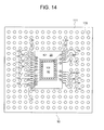
- FIG. 14 is a conceptual diagram showing an example of internal connections in the CSP and in the interconnect layer of those signals which are required to be externally connected to the external terminals 115 of the CSP of FIG. 13 .
- Signal names are identical with those shown in FIG. 6 .
- the reason for making connections to the external terminals 115 in a manner shown in FIG. 14 is that when the CSP is mounted on the board, the on-board wiring to the external terminals 115 situated on the inner side of the external terminal array increases in density as the pitch of the external terminals decreases making the on-board wiring more difficult.
- the external terminals to be externally interconnected on the board are chosen as practically as possible from among those situated close to each other on the inner side.
- FIG. 15 shows an example of on-board external connections between those external terminals to which the signal terminals are output as shown in FIG. 14 .
- FIGS. 16 a - 16 c i.e., independently connecting the chips to the external terminals without internally connecting them, can make the test environments of the individual chips in the MCM package identical with the test environments originally developed for the individual chips., as described in the embodiment 1.
- FIG. 16 a shows an example of module using a circuit board
- FIG. 16 b an example of a module using a lead frame
- FIG. 16 c an example of a module using a circuit board and a lead frame.
- Denoted 161 is a first LSI chip, 162 a second LSI chip, 163 resin, 164 wires, 165 lead frames, 166 thick film resistors, and 167 a chip capacitor.
- this invention When incorporating a plurality of chips into one package, this invention is characterized in that the connections between the chips are not brought into the package as practically as possible and that the terminals of each chip are drawn out of the package and individually connected to external terminals.
- This arrangement ensures that the environment under which each of the chips mounted in a single package is tested is very close to or identical with the environment under which each chip is tested as it is installed in its own package. This offers a high possibility that the existing test environment can be used as is, thus guaranteeing the test reliability. This also reduces the number of test development processes required to develop a new package, contributing to a reduction in the development cost and development period.
- test reliability cannot be guaranteed unless some measures are taken to eliminate influences of the in-package chip-to-chip connections.
- An example case of accommodating a part of the connections between a plurality of chips into the package may be where it is required to shorten the interconnecting wire lengths for faster processing.
- the present invention can be applied not only to the chips that are closely related with each other and directly connected on the board (chip A and chip B in FIG. 17 in a closely related group) but also to the chips which, though not directly connected, are deemed to constitute an indispensable combination to realize a certain function (chip D and chip E in a remotely related group). These applications are expected to produce the similar effects.
- FIG. 18 shows an example of package containing a combination of a DRAM as a memory and a controller that executes the image processing.
- FIG. 19 shows an example of package containing a combination of a DRAM and a flash memory. This type of package is expected to have growing demands in the future in such applications as cellular phones that require a large capacity of temporary memory for image communications.
- FIG. 21 shows another example of the semiconductor disk device 100 alternative to the embodiment 1, which is designed to facilitate the testing of a plurality of chips accommodated in the semiconductor package 10 .
- the semiconductor disk device 100 of the embodiment 7 has a test mode switching external terminal 17 formed in the semiconductor package 10 which receives a test mode switching signal from the external circuit.
- a plurality of chips 20 , 30 in the semiconductor package 10 are internally connected and connection selectors 61 , 62 are provided at intersections between the internal buses 311 and 312 and between the internal buses 313 , 314 and 315 .
- the selector 61 When a test mode for the controller chip 30 is specified according to the test mode switching signal received from the external circuit, the selector 61 connects the controller chip 30 through the internal bus 311 to the external terminal 12 and disconnects the internal bus 312 . At the same time, the selector 62 connects the internal buses 313 and 314 to connect the controller chip 30 to the external terminal 18 .
- the selector 61 connects the internal bus 311 on the external terminal 12 side to the internal bus 312 and disconnects the internal bus 311 on the controller side.
- the selector 62 connects the internal buses 314 and 315 to connect the memory chip 20 to the external terminal 18 and disconnects the internal bus 313 .
- the controller chip 30 or memory chip 20 can be tested independently by the test system connected to the external terminals 12 , 18 . This produces the similar effect to that obtained when the chips in the embodiment 1 are connected independently to the external terminals and tested.
- a normal mode signal is input to the test mode switching external terminal 17 .
- the selector 61 connects the internal buses 311 , 312 and the selector 62 connects the internal buses 313 , 314 , 315 .
- the controller chip 30 can access the expansion memory 50 connected to the external terminals 12 , 18 in the same hierarchy as the built-in memory 20 .
- connection selectors 61 , 62 have a decoder to decode the test mode switching signal.
- the decoder has a built-in switch means to control the internal bus, which is to be disconnected, at a high output impedance.
- the connection selectors 61 , 62 may be taken as a tri-state (3-state) output circuit arranged in each output circuit of the plurality of chips 20 , 30 .
- connection selectors 61 , 62 may be incorporated into the input/output terminal blocks of the controller chip 30 .
- the connection selectors 63 , 64 are incorporated in the controller chip 30 , connected to the input/output terminal blocks (electrode pads) 33 , 34 .
- the input/output terminal blocks 33 , 34 are expected to have an increased number of electrode pads for connection with external terminals and the memory chip 20 , they offer the advantage of being able to incorporate the connection selectors 63 , 64 in the controller chip 30 .
- the functions of the connection selectors 63 , 64 are virtually the same as those of the connection selectors 61 , 62 of FIG. 21, except that the connection selectors 63 , 64 switch the connections to the internal circuits of the controller.
- the test mode switching signal is commonly entered into the electrode pad 45 of the controller 30 .
- test mode switching signal terminal 22 shown in FIG. 21 and FIG. 22 need not be a dedicated external terminal but may not be provided when the test mode switching signal is replaced with a combination of a plurality of other signals.
- connection selectors 61 , 62 , 63 , 64 in the semiconductor package 10 as described above allows the chips to be individually tested under their own test environments in the same way as they are tested in the semiconductor disk device 100 of the embodiment 1.
- the semiconductor disk device 100 of this embodiment can accommodate in the semiconductor package 10 the interconnecting wires 312 , 313 , 315 between a plurality of chips.
- FIG. 23 shows a variation of the MCP type semiconductor disk device 100 explained in the embodiment 1 and 7.
- the semiconductor disk device 100 of this embodiment has internally connected between the controller 30 and the built-in memory 20 a signal path for a chip enable signal CE 1 by which the controller 30 selects and activates the built-in memory 20 .
- the controller 30 outputs through an external terminal 19 chip enable signals CE 2 , CEn for selecting the expansion memories 51 , 52 mounted outside the semiconductor disk device 100 . All other input/output signals necessary for the controller 30 to access the memory connect internally to the built-in memory 20 via the internal bus 316 .
- the internal bus 316 connects to the expansion memory interface 41 so that the controller 30 can access the expansion memories 51 , 52 via an expansion memory bus 301 . While in the embodiment of FIG.
- this embodiment is a semiconductor disk device constructed in the MCP configuration while the prior art is a semiconductor disk device constructed on a one-chip LSI.
- the expansion memory interface of this embodiment is the one that multiplexes address/data/command. If a part of the signals is brought out to the external terminals through which the controller 30 and the built-in memory 20 are externally connected as described above, the expansion memory interface 41 becomes an interface common to the expansion memories 51 , 52 and the built-in memory 20 . Thus, it is clearly different from the expansion memory interface of the prior art which is dedicated to only the expansion memory.
- FIG. 24 shows an example configuration of a single semiconductor disk LSI 60 incorporating a controller unit 70 and a memory unit 80 .
- the input/output blocks 73 , 74 , 81 , 82 of the units 70 , 80 are independently connected to the external terminals 12 , 13 , 14 , 15 , 16 of the semiconductor package 10 sealing the LSI chip, as in the embodiment 1.
- the external terminals are connected on the board to form the semiconductor disk device.
- the controller unit 70 accesses the memory unit 80 through the external terminal (memory interface) 12 , memory bus 301 and external terminal 14 .
- a semiconductor device including a first semiconductor chip and a second semiconductor chip in a single package, the semiconductor device comprising:
- a selector installed in a signal internal connecting portion between the first semiconductor chip, the second semiconductor chip and external terminals of the package to switch an internal connection
- test mode input external terminal for inputting a test mode signal to the selector
- a first test mode in which the selector, according to the test mode signal, independently connects input/output terminals of the first semiconductor chip to the external terminals of the package and disconnects the second semiconductor chip;
- a second test mode in which the selector, according to the test mode signal, independently connects input/output terminals of the second semiconductor chip to the external terminals of the package and disconnects the first semiconductor chip;
- a normal mode in which the selector, according to a normal mode signal, internally connects the first semiconductor chip and the second semiconductor chip.
- a semiconductor device wherein the selector is incorporated in an input/output terminal portion of the first semiconductor chip, and internal connections are made between the input/output terminals of the first semiconductor chip and the input/output terminals of the second semiconductor chip and between the input/output terminals of the first semiconductor chip and the external terminals of the package.
- test mode signal is replaced with a combination of a plurality of other signals and the test mode input external terminal is replaced with a plurality of other signal input external terminals.
- a semiconductor device including a first semiconductor chip and a second semiconductor chip in a single package
- signal electrode pads of the first semiconductor chip are connected inside the package in a one-to-one relationship to first external terminals of the package;
- signal electrode pads of the second semiconductor chip are connected inside the package in a one-to-one relationship to second external terminals of the package;
- a power supply terminal or a ground terminal is commonly connected to the first semiconductor chip and the second semiconductor chip.
- a semiconductor device wherein the first semiconductor chip is mounted on the second semiconductor chip, with a surface (back surface) of the first semiconductor chip opposite its circuit forming surface securely bonded to a circuit forming surface of the second semiconductor chip, and a support lead of a lead frame is securely bonded to the circuit forming surface of the second semiconductor chip and sealed with a resin.
- a semiconductor device according to any one of examples 1 to 5, wherein, of the external terminals independently connected to the input/output signal electrode pads of the first and second semiconductor chips, at least a pair of external terminals to be interconnected, one connected to the first semiconductor chip and one connected to the second semiconductor chip, is arranged so that these external terminals are set close to each other.
- a semiconductor device comprising:
- a host interface having a plurality of input/output external terminals for connection with a host unit
- controller chip to access-control the memory chip according to a memory access request received from the host unit through the host interface
- first external terminals and the second external terminals are externally interconnected to allow the controller to access the memory.
- a semiconductor device further including a plurality of third external terminals to input and output an access control signal for the controller chip to access-control an expansion memory connected outside the semiconductor device.
- a semiconductor device wherein, of the external terminals connected to the address/data input/output electrode pads of the controller chip and the memory chip, at least a pair of external terminals to be interconnected, one connected to the controller chip and one connected to the memory chip, is arranged so that these external terminals are set close to each other.
- a semiconductor disk device comprising:
- the semiconductor device mounted on a mother board, the semiconductor device having:
- a host interface having a plurality of input/output external terminals for connection with a host unit
- controller chip to access-control the memory chip according to a memory access request received from the host unit through the host interface
- first external terminals and the second external terminals are interconnected by wires on the mother board.
- a semiconductor device comprising a control unit and a memory unit in a single semiconductor chip
- first and second external terminals of the semiconductor chip are interconnected outside the semiconductor chip to complete the connection between the signal output of the control unit and the signal input of the memory unit.
- a semiconductor device having a control unit and a memory unit mounted in a single semiconductor chip
- a path for inputting an output signal A of the control unit into the memory chip comprises:
- control unit has an interface function to respond to an access from a host unit and an interface function to convert the access from the host unit into an access unique to the memory unit and access-control the memory unit.
- a semiconductor device according to any one of examples 1 to 3, wherein the first semiconductor chip is an SRAM or a controller and the second semiconductor chip is a flash memory (block erase type EEPROM) or a DRAM.
- a semiconductor device wherein when either the first or second semiconductor chip fails during a test, the failed semiconductor chip is taken out of service and only the remaining semiconductor chip is allowed to operate.
- a semiconductor disk device comprising:
- a semiconductor device having accommodated in a single package a memory chip, a host interface having a plurality of input/output external terminals for connection with a host unit, a controller chip to access-control the memory chip according to a memory access request received from the host unit through the host interface, and a memory interface having a plurality of input/output external terminals for the controller chip to access an external expansion memory;
- a semiconductor disk device wherein the semiconductor device has a package structure in which the memory chip and the controller chip are stacked and sealed with resin.
- a semiconductor disk device wherein the expansion memory is in the form of a package mounted on the mother board, the package incorporating a plurality of memory chips stacked and sealed with resin.
- a plurality of kinds of semiconductor chips are accommodated in a single package to reduce the mounting area. Further, the internal connection among the chips inside the package is precluded as practically as possible and the terminals (electrode pads) of the chips are independently connected to the external terminals of the package.
- this arrangement eliminates influences of signals from other chips than the one being tested and influences of leakage currents. It is therefore possible to provide an environment under which the individual chips can be tested independently.
- the existing test system which was originally developed for the individual chip testing can be used as is or with only a slight modification. Hence, performing the test on the chips individually can guarantee the reliability of the test. This in turn eliminates the need to develop a new test system, keeping the product development TAT and cost low.
- test selector in the package and to select a desired internal connection according to a mode signal to test the chips independently.
- the test system originally developed for the individual chip testing can be used with the similar effects.
- the selector needs to be installed on the internal wires inside the package, or in the controller chip.
Abstract
Description
| TABLE 1 | |||||
| Terminal | Terminal | ||||
| # | name | Function | # | name | Function |
| 1 | Vss | Ground | 51 | H_D(5) | Data 5 |
| 2 | Vcc | Power supply | 52 | H_D(6) | Data 6 |
| 3 | Vccf | Power supply | 53 | H_D(11) | Data 11 |
| (flash) | |||||
| 4 | /RES | Reset | 54 | H_D(12) | Data 12 |
| 5 | RDY//Busy | Ready/busy | 55 | H_D(13) | Data 13 |
| 6 | /CDE | Command data | 56 | Vss | Ground |
| enable | |||||
| 7 | /OE | Output enable | 57 | H_D(14) | Data 14 |
| 8 | Vss | Ground | 58 | H_D(7) | Data 7 |
| 9 | I/O0 | Input/output 0 | 59 | H_CE1 | Chip enable |
| 1 | |||||
| 10 | I/O1 | Input/output 1 | 60 | H_A(10) | Address 10 |
| 11 | F_RDY_2 | Ready (for | 61 | H_OE | output |
| bank 2) | enable | ||||
| 12 | I/O2 | Input/output 2 | 62 | H_D(15) | Data 15 |
| 13 | F_RES | Reset | 63 | H_CE2 | Chip enable |
| 2 | |||||
| 14 | I/O3 | Input/output 3 | 64 | H_IORD | Read data |
| control | |||||
| 15 | TEST1 | Diagnostic | 65 | H_IOWR | Write data |
| mode selection | control | ||||
| 1 | |||||
| 16 | Vcc | Power supply | 66 | Vcc | Power supply |
| 17 | Vccf | Power supply | 67 | H_A(9) | Address 9 |
| (flash) | |||||
| 18 | I/O4 | Input/output 4 | 68 | H_A(8) | Address 8 |
| 19 | I/O5 | Input/output 5 | 69 | H_A(7) | Address 7 |
| 20 | I/O6 | Input/output 6 | 70 | H_A(6) | Address 6 |
| 21 | I/O7 | Input/output 7 | 71 | Vss | Ground |
| 22 | F_CEA_1 | Chip enable 1 | 72 | H_WE | Write enable |
| 23 | F_CEA_2 | Chip enable 2 | 73 | H_IREQ | Interrupt |
| request | |||||
| 24 | Vcc | Power supply | 74 | CSEL | Card select |
| 25 | SC | Serial clock | 75 | TEST2 | Diagnostic |
| input 1 | mode | ||||
| selection 2 | |||||
| 26 | F_SC_A1 | Serial clock | 76 | H_RESET | Reset |
| output 1 | |||||
| 27 | /WE | Write enable | 77 | WAIT | Wait |
| 28 | /CE | Chip enable | 78 | H_A(5) | Address 5 |
| 29 | Vss | Ground | 79 | H_A(4) | Address 4 |
| 30 | F_SC_A2 | Serial clock | 80 | H_A(3) | Address 3 |
| output 2 | |||||
| 31 | Vss | Ground | 81 | H_A(2) | Address 2 |
| 32 | F_CEA_3 | Chip enable 3 | 82 | H_INPACK | Input |
| acknowledge | |||||
| 33 | F_CEA_4 | Chip enable 4 | 83 | H_REG | Register |
| 34 | F_CEA_5 | Chip enable 5 | 84 | DASP | Handshake |
| control | |||||
| 35 | F_WEA | Write enable | 85 | H_STSCHG | Status |
| signal | |||||
| 36 | F_DA(7) | Data 7 | 86 | H_A(1) | Address 1 |
| 37 | F_DA(6) | Data 6 | 87 | H_A(0) | Address 0 |
| 38 | F_DA(5) | Data 5 | 88 | H_D(0) | Data 0 |
| 39 | Vcc | Power supply | 89 | H_D(1) | Data 1 |
| 40 | F_DA(4) | Data 4 | 90 | H_D(2) | Data 2 |
| 41 | F_DA(3) | Data 3 | 91 | H_IOIS16 | 16-bit |
| assert | |||||
| signal | |||||
| 42 | F_DA(2) | Data 2 | 92 | H_D(8) | Data 8 |
| 43 | F_DA(1) | Data 1 | 93 | H_D(9) | Data 9 |
| 44 | F_DA(0) | Data 0 | 94 | H_D(10) | Data 10 |
| 45 | F_OEA | Output enable | 95 | Vcc | Power supply |
| 46 | F_CDEA | Command data | 96 | PORST | Port |
| enable | |||||
| 47 | F_RDY_1 | Ready signal 1 | 97 | TEST3 | Diagnostic |
| mode | |||||
| selection 3 | |||||
| 48 | Vcc | Power supply | 98 | TEST4 | Diagnostic |
| mode | |||||
| selection 4 | |||||
| 49 | H_D(3) | Data 3 | 99 | XIN | Quartz |
| oscillation | |||||
| (IN) | |||||
| 50 | H_D(4) | Data 4 | 100 | XOUT | Quartz |
| oscillation | |||||
| (OUT) | |||||
| TABLE 2 | |||||
| First | Second | Third | Fourth | ||
| bus cycle | bus cycle | bus cycle | bus cycle | ||
| Oper- | Oper- | Oper- | Oper- | ||||||
| Bus | ation | Data | ation | Data | ation | Data | ation | Data | |
| Command | cycles | mode | in | mode | in/out | mode | in | mode | in |
| Read | 3 | Write | 00H | Write | SA(1) | Write | SA(2) | ||
| Erase | 4 | Write | 20H | Write | SA(1) | Write | SA(2) | Write | B0H |
| (Single | |||||||||
| sector) | |||||||||
| Erase | 4 | Write | 7FH | Write | BA(1) | Write | BA(2) | Write | B0H |
| (Block) | |||||||||
| Additional | 4 | Write | 10H | Write | SA(1) | Write | SA(2) | Write | 40H |
| write | |||||||||
| Rewrite | 4 | Write | 1FH | Write | SA(1) | Write | SA(2) | Write | 40H |
| (Pre-erase) | |||||||||
| Additional | 4 | Write | 0FH | Write | SA(1) | Write | SA(2) | Write | 40H |
| write | |||||||||
| (Control | |||||||||
| bytes) | |||||||||
| Erase verify | 4 | Write | A0H | Write | SA(1) | Write | SA(2) | Write | A0H |
| Reset | 1 | Write | FFH | ||||||
| Status | 2 | Write | 70H | Read | SRD | ||||
| register | |||||||||
| Read | |||||||||
| Status | 1 | Write | 50H | ||||||
| register | |||||||||
| Clear | |||||||||
| SA(1) = Sector address (A0 to A7), SA(2) = Sector address (A8 to A13), BA(1) = Block address (A3 to A7), BA(2) = Block address (A8 to A13) [Entering A0 to A2 is not required], SRD = Status register data | |||||||||
| TABLE 3 | |||
| Chip A | Chip B | ||
| SRAM | Flash | ||
| SRAM | DRAM | ||
| Controller | Flash | ||
| Controller | DRAM | ||
Claims (13)
Priority Applications (3)
| Application Number | Priority Date | Filing Date | Title |
|---|---|---|---|
| US09/930,942 US6531773B2 (en) | 2000-03-03 | 2001-08-17 | Semiconductor device |
| US09/930,943 US6492727B2 (en) | 2000-03-03 | 2001-08-17 | Semiconductor device |
| US10/331,650 US20030151134A1 (en) | 2000-03-03 | 2002-12-31 | Semiconductor device |
Applications Claiming Priority (2)
| Application Number | Priority Date | Filing Date | Title |
|---|---|---|---|
| JP2000-063285 | 2000-03-03 | ||
| JP2000063285A JP3955712B2 (en) | 2000-03-03 | 2000-03-03 | Semiconductor device |
Related Child Applications (2)
| Application Number | Title | Priority Date | Filing Date |
|---|---|---|---|
| US09/930,943 Continuation US6492727B2 (en) | 2000-03-03 | 2001-08-17 | Semiconductor device |
| US09/930,942 Continuation US6531773B2 (en) | 2000-03-03 | 2001-08-17 | Semiconductor device |
Publications (2)
| Publication Number | Publication Date |
|---|---|
| US20020011650A1 US20020011650A1 (en) | 2002-01-31 |
| US6501173B2 true US6501173B2 (en) | 2002-12-31 |
Family
ID=18583176
Family Applications (4)
| Application Number | Title | Priority Date | Filing Date |
|---|---|---|---|
| US09/797,719 Expired - Lifetime US6501173B2 (en) | 2000-03-03 | 2001-03-05 | Semiconductor device |
| US09/930,942 Expired - Lifetime US6531773B2 (en) | 2000-03-03 | 2001-08-17 | Semiconductor device |
| US09/930,943 Expired - Lifetime US6492727B2 (en) | 2000-03-03 | 2001-08-17 | Semiconductor device |
| US10/331,650 Abandoned US20030151134A1 (en) | 2000-03-03 | 2002-12-31 | Semiconductor device |
Family Applications After (3)
| Application Number | Title | Priority Date | Filing Date |
|---|---|---|---|
| US09/930,942 Expired - Lifetime US6531773B2 (en) | 2000-03-03 | 2001-08-17 | Semiconductor device |
| US09/930,943 Expired - Lifetime US6492727B2 (en) | 2000-03-03 | 2001-08-17 | Semiconductor device |
| US10/331,650 Abandoned US20030151134A1 (en) | 2000-03-03 | 2002-12-31 | Semiconductor device |
Country Status (8)
| Country | Link |
|---|---|
| US (4) | US6501173B2 (en) |
| JP (1) | JP3955712B2 (en) |
| KR (2) | KR100842140B1 (en) |
| CN (1) | CN1257552C (en) |
| AU (1) | AU2001236028A1 (en) |
| MY (1) | MY124929A (en) |
| TW (2) | TW552667B (en) |
| WO (1) | WO2001065605A1 (en) |
Cited By (8)
| Publication number | Priority date | Publication date | Assignee | Title |
|---|---|---|---|---|
| US6653727B2 (en) * | 2002-04-17 | 2003-11-25 | Samsung Electronics Co., Ltd. | Semiconductor chip package with direction-flexible mountability |
| US20040016939A1 (en) * | 2002-07-26 | 2004-01-29 | Masayuki Akiba | Encapsulation of a stack of semiconductor dice |
| US20050077600A1 (en) * | 2003-09-30 | 2005-04-14 | Matsushita Electric Industrial Co., Ltd. | Semiconductor device |
| US20060095622A1 (en) * | 2004-10-28 | 2006-05-04 | Spansion, Llc | System and method for improved memory performance in a mobile device |
| US20080057624A1 (en) * | 2005-09-07 | 2008-03-06 | Lee Dae W | Stack type semiconductor package utilizing solder coated stacking protrusions and method for manufacturing the same |
| US20100007014A1 (en) * | 2008-07-11 | 2010-01-14 | Kabushiki Kaisha Toshiba | Semiconductor device |
| US8055978B2 (en) * | 2007-01-29 | 2011-11-08 | Samsung Electronics Co., Ltd. | Semiconductor memory system performing data error correction using flag cell array of buffer memory |
| US20120036369A1 (en) * | 2010-08-06 | 2012-02-09 | Phison Electronics Corp. | Memory identification code generation method, management method, controller, and storage system |
Families Citing this family (105)
| Publication number | Priority date | Publication date | Assignee | Title |
|---|---|---|---|---|
| JP2002033436A (en) * | 2000-07-14 | 2002-01-31 | Hitachi Ltd | Semiconductor device |
| US7444575B2 (en) * | 2000-09-21 | 2008-10-28 | Inapac Technology, Inc. | Architecture and method for testing of an integrated circuit device |
| US7006940B1 (en) * | 2002-11-27 | 2006-02-28 | Inapac Technology, Inc. | Set up for a first integrated circuit chip to allow for testing of a co-packaged second integrated circuit chip |
| JP2002124626A (en) * | 2000-10-16 | 2002-04-26 | Hitachi Ltd | Semiconductor device |
| US6843421B2 (en) * | 2001-08-13 | 2005-01-18 | Matrix Semiconductor, Inc. | Molded memory module and method of making the module absent a substrate support |
| US7313740B2 (en) * | 2002-07-25 | 2007-12-25 | Inapac Technology, Inc. | Internally generating patterns for testing in an integrated circuit device |
| US7404117B2 (en) * | 2005-10-24 | 2008-07-22 | Inapac Technology, Inc. | Component testing and recovery |
| US8166361B2 (en) * | 2001-09-28 | 2012-04-24 | Rambus Inc. | Integrated circuit testing module configured for set-up and hold time testing |
| US8001439B2 (en) | 2001-09-28 | 2011-08-16 | Rambus Inc. | Integrated circuit testing module including signal shaping interface |
| US7245141B2 (en) * | 2002-11-27 | 2007-07-17 | Inapac Technology, Inc. | Shared bond pad for testing a memory within a packaged semiconductor device |
| US8286046B2 (en) | 2001-09-28 | 2012-10-09 | Rambus Inc. | Integrated circuit testing module including signal shaping interface |
| US6778436B2 (en) * | 2001-10-10 | 2004-08-17 | Fong Piau | Apparatus and architecture for a compact flash memory controller |
| JP4005813B2 (en) | 2002-01-28 | 2007-11-14 | 株式会社東芝 | Semiconductor device |
| US6617181B1 (en) * | 2002-02-01 | 2003-09-09 | Lsi Logic Corporation | Flip chip testing |
| US6731011B2 (en) * | 2002-02-19 | 2004-05-04 | Matrix Semiconductor, Inc. | Memory module having interconnected and stacked integrated circuits |
| US7941675B2 (en) | 2002-12-31 | 2011-05-10 | Burr James B | Adaptive power control |
| US7112978B1 (en) | 2002-04-16 | 2006-09-26 | Transmeta Corporation | Frequency specific closed loop feedback control of integrated circuits |
| US7309999B2 (en) * | 2002-11-27 | 2007-12-18 | Inapac Technology, Inc. | Electronic device having an interface supported testing mode |
| US7466160B2 (en) * | 2002-11-27 | 2008-12-16 | Inapac Technology, Inc. | Shared memory bus architecture for system with processor and memory units |
| US8063650B2 (en) | 2002-11-27 | 2011-11-22 | Rambus Inc. | Testing fuse configurations in semiconductor devices |
| US7673193B1 (en) * | 2005-08-18 | 2010-03-02 | Rambus Inc. | Processor-memory unit for use in system-in-package and system-in-module devices |
| US7228242B2 (en) * | 2002-12-31 | 2007-06-05 | Transmeta Corporation | Adaptive power control based on pre package characterization of integrated circuits |
| US7953990B2 (en) | 2002-12-31 | 2011-05-31 | Stewart Thomas E | Adaptive power control based on post package characterization of integrated circuits |
| JP4149289B2 (en) * | 2003-03-12 | 2008-09-10 | 株式会社ルネサステクノロジ | Semiconductor device |
| KR100481184B1 (en) * | 2003-03-26 | 2005-04-07 | 삼성전자주식회사 | Semiconductor memory integrated circuit |
| JP4190961B2 (en) * | 2003-06-26 | 2008-12-03 | 株式会社ルネサステクノロジ | Multi-chip module |
| US6977433B2 (en) * | 2003-10-28 | 2005-12-20 | Seagate Technology Llc | Multi function package |
| US7287115B2 (en) * | 2003-10-30 | 2007-10-23 | Kabushiki Kaisha Toshiba | Multi-chip package type memory system |
| US7129771B1 (en) | 2003-12-23 | 2006-10-31 | Transmeta Corporation | Servo loop for well bias voltage source |
| US7692477B1 (en) | 2003-12-23 | 2010-04-06 | Tien-Min Chen | Precise control component for a substrate potential regulation circuit |
| US7649402B1 (en) | 2003-12-23 | 2010-01-19 | Tien-Min Chen | Feedback-controlled body-bias voltage source |
| US7012461B1 (en) | 2003-12-23 | 2006-03-14 | Transmeta Corporation | Stabilization component for a substrate potential regulation circuit |
| TWI237889B (en) * | 2004-01-16 | 2005-08-11 | Optimum Care Int Tech Inc | Chip leadframe module |
| JP4343727B2 (en) * | 2004-02-13 | 2009-10-14 | 株式会社ルネサステクノロジ | Semiconductor device |
| JP4885426B2 (en) * | 2004-03-12 | 2012-02-29 | ルネサスエレクトロニクス株式会社 | Semiconductor memory device, semiconductor device and manufacturing method thereof |
| JP4157065B2 (en) * | 2004-03-29 | 2008-09-24 | 株式会社東芝 | Semiconductor memory device |
| KR100564621B1 (en) | 2004-04-08 | 2006-03-28 | 삼성전자주식회사 | Buffered memory module package and module-stacked package comprising the module package |
| TWI237883B (en) * | 2004-05-11 | 2005-08-11 | Via Tech Inc | Chip embedded package structure and process thereof |
| JP4455158B2 (en) * | 2004-05-20 | 2010-04-21 | 株式会社ルネサステクノロジ | Semiconductor device |
| US7774625B1 (en) | 2004-06-22 | 2010-08-10 | Eric Chien-Li Sheng | Adaptive voltage control by accessing information stored within and specific to a microprocessor |
| US7562233B1 (en) | 2004-06-22 | 2009-07-14 | Transmeta Corporation | Adaptive control of operating and body bias voltages |
| JP4752369B2 (en) * | 2004-08-24 | 2011-08-17 | ソニー株式会社 | Semiconductor device and substrate |
| JP4003780B2 (en) | 2004-09-17 | 2007-11-07 | カシオ計算機株式会社 | Semiconductor device and manufacturing method thereof |
| KR100588337B1 (en) | 2005-02-11 | 2006-06-09 | 삼성전자주식회사 | Semiconductor device with multiple pads of common functionality, and multi chip package using the same |
| KR100699838B1 (en) | 2005-04-13 | 2007-03-27 | 삼성전자주식회사 | A semiconductor device including the ROM interface PAD |
| JP2007019415A (en) | 2005-07-11 | 2007-01-25 | Renesas Technology Corp | Semiconductor device and its manufacturing method |
| US7602050B2 (en) * | 2005-07-18 | 2009-10-13 | Qualcomm Incorporated | Integrated circuit packaging |
| US7779311B2 (en) * | 2005-10-24 | 2010-08-17 | Rambus Inc. | Testing and recovery in a multilayer device |
| JP4626490B2 (en) * | 2005-11-07 | 2011-02-09 | ソニー株式会社 | Circuit equipment |
| US7631152B1 (en) * | 2005-11-28 | 2009-12-08 | Nvidia Corporation | Determining memory flush states for selective heterogeneous memory flushes |
| US7443011B2 (en) * | 2006-02-10 | 2008-10-28 | Marvell International Technology Ltd. | System and method for routing supply voltages or other signals between side-by-side die and a lead frame for system in a package (SIP) devices |
| US7990727B1 (en) * | 2006-04-03 | 2011-08-02 | Aprolase Development Co., Llc | Ball grid array stack |
| JP2007335809A (en) * | 2006-06-19 | 2007-12-27 | Nec Electronics Corp | Semiconductor device and method for controlling operation of semiconductor device |
| US7761626B2 (en) * | 2006-09-28 | 2010-07-20 | Virident Systems, Inc. | Methods for main memory in a system with a memory controller configured to control access to non-volatile memory, and related technologies |
| US8949555B1 (en) | 2007-08-30 | 2015-02-03 | Virident Systems, Inc. | Methods for sustained read and write performance with non-volatile memory |
| WO2008040028A2 (en) * | 2006-09-28 | 2008-04-03 | Virident Systems, Inc. | Systems, methods, and apparatus with programmable memory control for heterogeneous main memory |
| US7761625B2 (en) * | 2006-09-28 | 2010-07-20 | Virident Systems, Inc. | Methods for main memory with non-volatile type memory modules, and related technologies |
| US9984012B2 (en) | 2006-09-28 | 2018-05-29 | Virident Systems, Llc | Read writeable randomly accessible non-volatile memory modules |
| US20080082750A1 (en) * | 2006-09-28 | 2008-04-03 | Okin Kenneth A | Methods of communicating to, memory modules in a memory channel |
| US8074022B2 (en) * | 2006-09-28 | 2011-12-06 | Virident Systems, Inc. | Programmable heterogeneous memory controllers for main memory with different memory modules |
| US8806116B2 (en) * | 2008-02-12 | 2014-08-12 | Virident Systems, Inc. | Memory modules for two-dimensional main memory |
| US7761624B2 (en) * | 2006-09-28 | 2010-07-20 | Virident Systems, Inc. | Systems and apparatus for main memory with non-volatile type memory modules, and related technologies |
| US7761623B2 (en) * | 2006-09-28 | 2010-07-20 | Virident Systems, Inc. | Main memory in a system with a memory controller configured to control access to non-volatile memory, and related technologies |
| US20080079148A1 (en) * | 2006-09-30 | 2008-04-03 | Silicon Laboratories Inc. | Package for mixed signal mcu with minimal pin count |
| WO2008042403A2 (en) | 2006-10-03 | 2008-04-10 | Inapac Technologies, Inc. | Memory accessing circuit system |
| US8189328B2 (en) * | 2006-10-23 | 2012-05-29 | Virident Systems, Inc. | Methods and apparatus of dual inline memory modules for flash memory |
| US7561027B2 (en) * | 2006-10-26 | 2009-07-14 | Hewlett-Packard Development Company, L.P. | Sensing device |
| KR100850204B1 (en) * | 2006-11-04 | 2008-08-04 | 삼성전자주식회사 | Method and apparatus for generating high-frequency command and address signals for high-speed semiconductor memory device testing |
| KR100845527B1 (en) * | 2006-12-06 | 2008-07-10 | 삼성전자주식회사 | Memory device and method of contolling clock cycle of Memory Controller |
| KR100843718B1 (en) * | 2007-01-25 | 2008-07-04 | 삼성전자주식회사 | Semiconductor packages having immunity against void due to adhesive material and methods of forming the same |
| ITMI20070933A1 (en) * | 2007-05-08 | 2008-11-09 | St Microelectronics Srl | MULTI PIASTRINA ELECTRONIC SYSTEM |
| JP4469877B2 (en) * | 2007-07-12 | 2010-06-02 | 株式会社東芝 | Electronic equipment |
| US9921896B2 (en) | 2007-08-30 | 2018-03-20 | Virident Systems, Llc | Shutdowns and data recovery to avoid read errors weak pages in a non-volatile memory system |
| US7898091B2 (en) * | 2007-10-02 | 2011-03-01 | Sandisk Corporation | Multi-host interface controller with USB PHY/analog functions integrated in a single package |
| JP2009134573A (en) * | 2007-11-30 | 2009-06-18 | Nec Corp | Multi-chip semiconductor device and data transfer method |
| WO2009102821A2 (en) * | 2008-02-12 | 2009-08-20 | Virident Systems, Inc. | Methods and apparatus for two-dimensional main memory |
| US8307180B2 (en) | 2008-02-28 | 2012-11-06 | Nokia Corporation | Extended utilization area for a memory device |
| US20110075387A1 (en) * | 2008-05-21 | 2011-03-31 | Homer Steven S | Strain Measurement Chips For Printed Circuit Boards |
| US9513695B2 (en) | 2008-06-24 | 2016-12-06 | Virident Systems, Inc. | Methods of managing power in network computer systems |
| US8745314B1 (en) | 2008-06-24 | 2014-06-03 | Virident Systems, Inc. | Methods for a random read and read/write block accessible memory |
| JP2010185677A (en) * | 2009-02-10 | 2010-08-26 | Toshiba Corp | Device and method for measuring power supply current |
| US8874824B2 (en) | 2009-06-04 | 2014-10-28 | Memory Technologies, LLC | Apparatus and method to share host system RAM with mass storage memory RAM |
| JP5218319B2 (en) * | 2009-07-27 | 2013-06-26 | 富士通セミコンダクター株式会社 | Semiconductor substrate |
| JP5581627B2 (en) * | 2009-08-05 | 2014-09-03 | セイコーエプソン株式会社 | Integrated circuit device and electronic apparatus |
| JP2011129894A (en) * | 2009-11-18 | 2011-06-30 | Toshiba Corp | Semiconductor device |
| EP2333830B1 (en) * | 2009-12-07 | 2014-09-03 | STMicroelectronics (Research & Development) Limited | a package comprising a first and a second die coupled by a multiplexed bus |
| EP2339795B1 (en) * | 2009-12-07 | 2013-08-14 | STMicroelectronics (Research & Development) Limited | Inter-chip communication interface for a multi-chip package |
| EP2339476B1 (en) * | 2009-12-07 | 2012-08-15 | STMicroelectronics (Research & Development) Limited | Interface connecting dies in an IC package |
| EP2339475A1 (en) * | 2009-12-07 | 2011-06-29 | STMicroelectronics (Research & Development) Limited | Inter-chip communication interface for a multi-chip package |
| EP2333673B1 (en) * | 2009-12-07 | 2014-04-16 | STMicroelectronics (Research & Development) Limited | Signal sampling and transfer |
| EP2330514B1 (en) | 2009-12-07 | 2018-12-05 | STMicroelectronics (Research & Development) Limited | An integrated circuit package |
| TW201134317A (en) * | 2010-03-29 | 2011-10-01 | Hon Hai Prec Ind Co Ltd | Pins assignment for circuit board |
| TW201225249A (en) | 2010-12-08 | 2012-06-16 | Ind Tech Res Inst | Stacked structure and stacked method for three-dimensional integrated circuit |
| US8521937B2 (en) | 2011-02-16 | 2013-08-27 | Stmicroelectronics (Grenoble 2) Sas | Method and apparatus for interfacing multiple dies with mapping to modify source identity |
| WO2012163100A1 (en) * | 2011-05-30 | 2012-12-06 | 深圳市江波龙电子有限公司 | Semiconductor chip and storage device |
| US9417998B2 (en) | 2012-01-26 | 2016-08-16 | Memory Technologies Llc | Apparatus and method to provide cache move with non-volatile mass memory system |
| KR20130092110A (en) | 2012-02-10 | 2013-08-20 | 삼성전자주식회사 | Embeded solid state disk and solid state disk |
| US9311226B2 (en) | 2012-04-20 | 2016-04-12 | Memory Technologies Llc | Managing operational state data of a memory module using host memory in association with state change |
| KR102104060B1 (en) | 2013-04-29 | 2020-04-23 | 삼성전자 주식회사 | POP(Package On Package) semiconductor structure |
| US20150075849A1 (en) * | 2013-09-17 | 2015-03-19 | Jia Lin Yap | Semiconductor device and lead frame with interposer |
| US9766823B2 (en) | 2013-12-12 | 2017-09-19 | Memory Technologies Llc | Channel optimized storage modules |
| KR102219296B1 (en) | 2014-08-14 | 2021-02-23 | 삼성전자 주식회사 | Semiconductor package |
| CN109525237B (en) * | 2017-09-18 | 2020-10-09 | 华为技术有限公司 | Interface unit and interface module and chip with same |
| KR102605145B1 (en) * | 2018-07-13 | 2023-11-24 | 에스케이하이닉스 주식회사 | Semiconductor apparatus including a plurality of dies operating as a plurality of channels |
| TWI763070B (en) * | 2020-10-05 | 2022-05-01 | 新唐科技股份有限公司 | Semiconductor device and controlling method thereof |
Citations (17)
| Publication number | Priority date | Publication date | Assignee | Title |
|---|---|---|---|---|
| JPH0513662A (en) | 1991-07-03 | 1993-01-22 | Nippondenso Co Ltd | Multichip module |
| JPH065386A (en) | 1992-06-19 | 1994-01-14 | Kobe Steel Ltd | Electronic cyclotron resonance device |
| JPH06250799A (en) | 1993-02-26 | 1994-09-09 | Toshiba Corp | Semiconductor disk device and computer system using the same |
| JPH06333848A (en) | 1993-05-27 | 1994-12-02 | Hitachi Ltd | Plasma generating device |
| JPH08316407A (en) | 1995-05-15 | 1996-11-29 | Nec Corp | Manufacture of composite semiconductor package |
| JPH09508496A (en) | 1994-02-07 | 1997-08-26 | シーメンス アクチエンゲゼルシヤフト | Semiconductor memory device having a plurality of memory chips in a common package |
| US5754567A (en) * | 1996-10-15 | 1998-05-19 | Micron Quantum Devices, Inc. | Write reduction in flash memory systems through ECC usage |
| JPH1119370A (en) | 1997-07-08 | 1999-01-26 | Akiko Shinoda | Foldable auxiliary table for sewing machine |
| JPH1186546A (en) | 1997-09-09 | 1999-03-30 | Fujitsu Ltd | Semiconductor device and semiconductor system |
| JPH11163255A (en) | 1997-09-29 | 1999-06-18 | Hitachi Ltd | Semiconductor device and manufacture thereof and electronic device |
| US5958079A (en) * | 1997-01-08 | 1999-09-28 | Mitsubishi Denki Kabushiki Kaisha | Memory card with error correction scheme requiring reducing memory capacity |
| JPH11354714A (en) | 1998-05-28 | 1999-12-24 | Samsung Electronics Co Ltd | Multi-chip package |
| JPH11354294A (en) | 1998-06-04 | 1999-12-24 | Naohisa Goto | Plasma processing device |
| US6084308A (en) * | 1998-06-30 | 2000-07-04 | National Semiconductor Corporation | Chip-on-chip integrated circuit package and method for making the same |
| US6119254A (en) * | 1997-12-23 | 2000-09-12 | Stmicroelectronics, N.V. | Hardware tracing/logging for highly integrated embedded controller device |
| US6256762B1 (en) * | 1997-01-23 | 2001-07-03 | Oki Electric Industry Co., Ltd. | Semiconductor disk device |
| US6291881B1 (en) * | 1999-03-04 | 2001-09-18 | United Microelectronics Corp. | Dual silicon chip package |
Family Cites Families (9)
| Publication number | Priority date | Publication date | Assignee | Title |
|---|---|---|---|---|
| JP2817486B2 (en) * | 1991-11-29 | 1998-10-30 | 日本電気株式会社 | Logic integrated circuit |
| US5917242A (en) * | 1996-05-20 | 1999-06-29 | Micron Technology, Inc. | Combination of semiconductor interconnect |
| JPH11219984A (en) * | 1997-11-06 | 1999-08-10 | Sharp Corp | Semiconductor device package, its manufacture and circuit board therefor |
| JP3481444B2 (en) * | 1998-01-14 | 2003-12-22 | シャープ株式会社 | Semiconductor device and manufacturing method thereof |
| JP3670853B2 (en) * | 1998-07-30 | 2005-07-13 | 三洋電機株式会社 | Semiconductor device |
| US6307256B1 (en) * | 1998-10-26 | 2001-10-23 | Apack Technologies Inc. | Semiconductor package with a stacked chip on a leadframe |
| JP3437107B2 (en) * | 1999-01-27 | 2003-08-18 | シャープ株式会社 | Resin-sealed semiconductor device |
| JP4164192B2 (en) * | 1999-05-12 | 2008-10-08 | 株式会社ルネサステクノロジ | Memory device equipped with semiconductor device |
| JP3606124B2 (en) * | 1999-08-19 | 2005-01-05 | セイコーエプソン株式会社 | Semiconductor integrated circuit device and electronic device |
-
2000
- 2000-03-03 JP JP2000063285A patent/JP3955712B2/en not_active Expired - Fee Related
-
2001
- 2001-03-01 AU AU2001236028A patent/AU2001236028A1/en not_active Abandoned
- 2001-03-01 KR KR1020027007976A patent/KR100842140B1/en not_active IP Right Cessation
- 2001-03-01 CN CNB01803246XA patent/CN1257552C/en not_active Expired - Fee Related
- 2001-03-01 MY MYPI20010957A patent/MY124929A/en unknown
- 2001-03-01 WO PCT/JP2001/001576 patent/WO2001065605A1/en active Application Filing
- 2001-03-01 KR KR1020077030438A patent/KR100828855B1/en not_active IP Right Cessation
- 2001-03-02 TW TW091104968A patent/TW552667B/en not_active IP Right Cessation
- 2001-03-02 TW TW090104846A patent/TW497199B/en not_active IP Right Cessation
- 2001-03-05 US US09/797,719 patent/US6501173B2/en not_active Expired - Lifetime
- 2001-08-17 US US09/930,942 patent/US6531773B2/en not_active Expired - Lifetime
- 2001-08-17 US US09/930,943 patent/US6492727B2/en not_active Expired - Lifetime
-
2002
- 2002-12-31 US US10/331,650 patent/US20030151134A1/en not_active Abandoned
Patent Citations (17)
| Publication number | Priority date | Publication date | Assignee | Title |
|---|---|---|---|---|
| JPH0513662A (en) | 1991-07-03 | 1993-01-22 | Nippondenso Co Ltd | Multichip module |
| JPH065386A (en) | 1992-06-19 | 1994-01-14 | Kobe Steel Ltd | Electronic cyclotron resonance device |
| JPH06250799A (en) | 1993-02-26 | 1994-09-09 | Toshiba Corp | Semiconductor disk device and computer system using the same |
| JPH06333848A (en) | 1993-05-27 | 1994-12-02 | Hitachi Ltd | Plasma generating device |
| JPH09508496A (en) | 1994-02-07 | 1997-08-26 | シーメンス アクチエンゲゼルシヤフト | Semiconductor memory device having a plurality of memory chips in a common package |
| JPH08316407A (en) | 1995-05-15 | 1996-11-29 | Nec Corp | Manufacture of composite semiconductor package |
| US5754567A (en) * | 1996-10-15 | 1998-05-19 | Micron Quantum Devices, Inc. | Write reduction in flash memory systems through ECC usage |
| US5958079A (en) * | 1997-01-08 | 1999-09-28 | Mitsubishi Denki Kabushiki Kaisha | Memory card with error correction scheme requiring reducing memory capacity |
| US6256762B1 (en) * | 1997-01-23 | 2001-07-03 | Oki Electric Industry Co., Ltd. | Semiconductor disk device |
| JPH1119370A (en) | 1997-07-08 | 1999-01-26 | Akiko Shinoda | Foldable auxiliary table for sewing machine |
| JPH1186546A (en) | 1997-09-09 | 1999-03-30 | Fujitsu Ltd | Semiconductor device and semiconductor system |
| JPH11163255A (en) | 1997-09-29 | 1999-06-18 | Hitachi Ltd | Semiconductor device and manufacture thereof and electronic device |
| US6119254A (en) * | 1997-12-23 | 2000-09-12 | Stmicroelectronics, N.V. | Hardware tracing/logging for highly integrated embedded controller device |
| JPH11354714A (en) | 1998-05-28 | 1999-12-24 | Samsung Electronics Co Ltd | Multi-chip package |
| JPH11354294A (en) | 1998-06-04 | 1999-12-24 | Naohisa Goto | Plasma processing device |
| US6084308A (en) * | 1998-06-30 | 2000-07-04 | National Semiconductor Corporation | Chip-on-chip integrated circuit package and method for making the same |
| US6291881B1 (en) * | 1999-03-04 | 2001-09-18 | United Microelectronics Corp. | Dual silicon chip package |
Cited By (14)
| Publication number | Priority date | Publication date | Assignee | Title |
|---|---|---|---|---|
| US6653727B2 (en) * | 2002-04-17 | 2003-11-25 | Samsung Electronics Co., Ltd. | Semiconductor chip package with direction-flexible mountability |
| US7132311B2 (en) * | 2002-07-26 | 2006-11-07 | Intel Corporation | Encapsulation of a stack of semiconductor dice |
| US20050085034A1 (en) * | 2002-07-26 | 2005-04-21 | Masayuki Akiba | Encapsulated stack of dice and support therefor |
| US7132739B2 (en) * | 2002-07-26 | 2006-11-07 | Intel Corporation | Encapsulated stack of dice and support therefor |
| US20040016939A1 (en) * | 2002-07-26 | 2004-01-29 | Masayuki Akiba | Encapsulation of a stack of semiconductor dice |
| US20050077600A1 (en) * | 2003-09-30 | 2005-04-14 | Matsushita Electric Industrial Co., Ltd. | Semiconductor device |
| US20060095622A1 (en) * | 2004-10-28 | 2006-05-04 | Spansion, Llc | System and method for improved memory performance in a mobile device |
| US20080057624A1 (en) * | 2005-09-07 | 2008-03-06 | Lee Dae W | Stack type semiconductor package utilizing solder coated stacking protrusions and method for manufacturing the same |
| US7462508B2 (en) * | 2005-09-07 | 2008-12-09 | Hynix Semiconductor Inc. | Stack type semiconductor package module utilizing solder coated stacking protrusions and method for manufacturing the same |
| US8055978B2 (en) * | 2007-01-29 | 2011-11-08 | Samsung Electronics Co., Ltd. | Semiconductor memory system performing data error correction using flag cell array of buffer memory |
| US20100007014A1 (en) * | 2008-07-11 | 2010-01-14 | Kabushiki Kaisha Toshiba | Semiconductor device |
| US20120036369A1 (en) * | 2010-08-06 | 2012-02-09 | Phison Electronics Corp. | Memory identification code generation method, management method, controller, and storage system |
| US8996933B2 (en) * | 2010-08-06 | 2015-03-31 | Phison Eletronics Corp. | Memory management method, controller, and storage system |
| TWI496161B (en) * | 2010-08-06 | 2015-08-11 | Phison Electronics Corp | Memory identification code generating method, management method, controller and storage system |
Also Published As
| Publication number | Publication date |
|---|---|
| US20030151134A1 (en) | 2003-08-14 |
| US20020017720A1 (en) | 2002-02-14 |
| KR20030036130A (en) | 2003-05-09 |
| TW497199B (en) | 2002-08-01 |
| KR20080008426A (en) | 2008-01-23 |
| MY124929A (en) | 2006-07-31 |
| KR100828855B1 (en) | 2008-05-09 |
| WO2001065605A1 (en) | 2001-09-07 |
| CN1257552C (en) | 2006-05-24 |
| US6492727B2 (en) | 2002-12-10 |
| AU2001236028A1 (en) | 2001-09-12 |
| KR100842140B1 (en) | 2008-06-27 |
| US6531773B2 (en) | 2003-03-11 |
| JP2001250908A (en) | 2001-09-14 |
| CN1398431A (en) | 2003-02-19 |
| TW552667B (en) | 2003-09-11 |
| US20020011650A1 (en) | 2002-01-31 |
| JP3955712B2 (en) | 2007-08-08 |
| US20020030270A1 (en) | 2002-03-14 |
Similar Documents
| Publication | Publication Date | Title |
|---|---|---|
| US6501173B2 (en) | Semiconductor device | |
| US6777801B2 (en) | Semiconductor device and method of manufacturing same | |
| US7355877B2 (en) | Semiconductor device | |
| US5946545A (en) | Semiconductor stack structures and fabrication/sparing methods utilizing programmable spare circuit | |
| US8338962B2 (en) | Semiconductor package substrate and semiconductor package having the same | |
| JP2003007963A (en) | Semiconductor memory device and its manufacturing method | |
| US20240028529A1 (en) | Memory system | |
| US20060261847A1 (en) | Semiconductor integrated circuit device | |
| CN101447475A (en) | System-in-Package | |
| JP4471990B2 (en) | Semiconductor device | |
| US9070482B2 (en) | Multi-chip package semiconductor memory device | |
| JP3911365B2 (en) | Semiconductor memory device | |
| JP2004007017A (en) | Semiconductor device | |
| JP2004096123A (en) | Semiconductor device |
Legal Events
| Date | Code | Title | Description |
|---|---|---|---|
| AS | Assignment |
Owner name: HITACHI, LTD., JAPAN Free format text: ASSIGNMENT OF ASSIGNORS INTEREST;ASSIGNORS:NISHIZAWA, HIROTAKA;MASUDA, MASACHIKA;KANEMOTO, KOUICHI;AND OTHERS;REEL/FRAME:011587/0215 Effective date: 20010201 Owner name: HITACHI ULSI SYSTEMS CO., LTD., JAPAN Free format text: ASSIGNMENT OF ASSIGNORS INTEREST;ASSIGNORS:NISHIZAWA, HIROTAKA;MASUDA, MASACHIKA;KANEMOTO, KOUICHI;AND OTHERS;REEL/FRAME:011587/0215 Effective date: 20010201 |
|
| STCF | Information on status: patent grant |
Free format text: PATENTED CASE |
|
| FEPP | Fee payment procedure |
Free format text: PAYOR NUMBER ASSIGNED (ORIGINAL EVENT CODE: ASPN); ENTITY STATUS OF PATENT OWNER: LARGE ENTITY |
|
| FEPP | Fee payment procedure |
Free format text: PAYER NUMBER DE-ASSIGNED (ORIGINAL EVENT CODE: RMPN); ENTITY STATUS OF PATENT OWNER: LARGE ENTITY Free format text: PAYOR NUMBER ASSIGNED (ORIGINAL EVENT CODE: ASPN); ENTITY STATUS OF PATENT OWNER: LARGE ENTITY |
|
| FPAY | Fee payment |
Year of fee payment: 4 |
|
| FPAY | Fee payment |
Year of fee payment: 8 |
|
| AS | Assignment |
Owner name: RENESAS ELECTRONICS CORPORATION, JAPAN Free format text: ASSIGNMENT OF ASSIGNORS INTEREST;ASSIGNOR:HITACHI, LTD.;REEL/FRAME:026109/0976 Effective date: 20110307 |
|
| AS | Assignment |
Owner name: RENESAS ELECTRONICS CORPORATION, JAPAN Free format text: ASSIGNMENT OF ASSIGNORS INTEREST;ASSIGNOR:HITACHI ULSI SYSTEMS CO., LTD.;REEL/FRAME:032859/0252 Effective date: 20140326 |
|
| FPAY | Fee payment |
Year of fee payment: 12 |
|
| AS | Assignment |
Owner name: RENESAS ELECTRONICS CORPORATION, JAPAN Free format text: CHANGE OF ADDRESS;ASSIGNOR:RENESAS ELECTRONICS CORPORATION;REEL/FRAME:044928/0001 Effective date: 20150806 |