US6445413B1 - System for determining a video offset from dark photosensors in an image sensor array - Google Patents
System for determining a video offset from dark photosensors in an image sensor array Download PDFInfo
- Publication number
- US6445413B1 US6445413B1 US09/138,941 US13894198A US6445413B1 US 6445413 B1 US6445413 B1 US 6445413B1 US 13894198 A US13894198 A US 13894198A US 6445413 B1 US6445413 B1 US 6445413B1
- Authority
- US
- United States
- Prior art keywords
- photosensor
- dark
- photosensors
- signal
- reading
- Prior art date
- Legal status (The legal status is an assumption and is not a legal conclusion. Google has not performed a legal analysis and makes no representation as to the accuracy of the status listed.)
- Expired - Lifetime
Links
- 238000012935 Averaging Methods 0.000 claims abstract description 30
- 238000012937 correction Methods 0.000 claims description 70
- 239000003990 capacitor Substances 0.000 claims description 56
- 238000000034 method Methods 0.000 claims description 16
- 238000013461 design Methods 0.000 description 7
- 238000010586 diagram Methods 0.000 description 7
- 230000000694 effects Effects 0.000 description 6
- 101100100119 Homo sapiens TNFRSF10C gene Proteins 0.000 description 4
- 101100121770 Saccharomyces cerevisiae (strain ATCC 204508 / S288c) GID8 gene Proteins 0.000 description 4
- 101100009020 Schizosaccharomyces pombe (strain 972 / ATCC 24843) dcr1 gene Proteins 0.000 description 4
- XUIMIQQOPSSXEZ-UHFFFAOYSA-N Silicon Chemical group [Si] XUIMIQQOPSSXEZ-UHFFFAOYSA-N 0.000 description 4
- 102100040115 Tumor necrosis factor receptor superfamily member 10C Human genes 0.000 description 4
- 101000716068 Homo sapiens C-C chemokine receptor type 6 Proteins 0.000 description 3
- 102100040110 Tumor necrosis factor receptor superfamily member 10D Human genes 0.000 description 3
- 238000003491 array Methods 0.000 description 3
- 238000012986 modification Methods 0.000 description 3
- 230000004048 modification Effects 0.000 description 3
- 230000008569 process Effects 0.000 description 3
- XAGFODPZIPBFFR-UHFFFAOYSA-N aluminium Chemical compound [Al] XAGFODPZIPBFFR-UHFFFAOYSA-N 0.000 description 2
- 229910052782 aluminium Inorganic materials 0.000 description 2
- 230000000052 comparative effect Effects 0.000 description 2
- 230000002829 reductive effect Effects 0.000 description 2
- 230000009885 systemic effect Effects 0.000 description 2
- 238000009825 accumulation Methods 0.000 description 1
- 230000008901 benefit Effects 0.000 description 1
- 230000008859 change Effects 0.000 description 1
- 230000006870 function Effects 0.000 description 1
- 238000003384 imaging method Methods 0.000 description 1
- 238000010348 incorporation Methods 0.000 description 1
- 230000010354 integration Effects 0.000 description 1
- 230000003071 parasitic effect Effects 0.000 description 1
- 230000000505 pernicious effect Effects 0.000 description 1
- 238000012545 processing Methods 0.000 description 1
- 230000009467 reduction Effects 0.000 description 1
- 239000004065 semiconductor Substances 0.000 description 1
- 229910052710 silicon Inorganic materials 0.000 description 1
- 239000010703 silicon Substances 0.000 description 1
Images


Classifications
-
- H—ELECTRICITY
- H04—ELECTRIC COMMUNICATION TECHNIQUE
- H04N—PICTORIAL COMMUNICATION, e.g. TELEVISION
- H04N1/00—Scanning, transmission or reproduction of documents or the like, e.g. facsimile transmission; Details thereof
- H04N1/40—Picture signal circuits
- H04N1/407—Control or modification of tonal gradation or of extreme levels, e.g. background level
- H04N1/4076—Control or modification of tonal gradation or of extreme levels, e.g. background level dependent on references outside the picture
-
- H—ELECTRICITY
- H04—ELECTRIC COMMUNICATION TECHNIQUE
- H04N—PICTORIAL COMMUNICATION, e.g. TELEVISION
- H04N25/00—Circuitry of solid-state image sensors [SSIS]; Control thereof
- H04N25/60—Noise processing, e.g. detecting, correcting, reducing or removing noise
- H04N25/63—Noise processing, e.g. detecting, correcting, reducing or removing noise applied to dark current
Definitions
- the present invention relates to image sensor arrays used in raster input scanners.
- the invention relates to photosensitive chips wherein each photosensor outputs signals onto a common video line, and where there are provided dark photosensors for setting an offset level on the common video line.
- Image sensor arrays typically comprise a linear array of photosensors which raster scan an image bearing document and convert the microscopic image areas viewed by each photosensor to image signal charges. Following an integration period, the image signal charges are amplified and transferred as an analog video signal to a common output line or bus through successively actuated multiplexing transistors.
- a preferred design includes an array of photosensors of a width comparable to the width of a page being scanned, to permit one-to-one imaging without reductive optics.
- relatively large silicon structures must be used to define the large number of photosensors.
- a preferred technique to create such a large array is to make the array out of several butted silicon chips. In one proposed design, an array is intended to be made of 20 silicon chips, butted end-to-end, each chip having 248 active photosensors spaced at 400 photosensors per inch.
- the “raw signal” coming out of the photosensors during the scanning process is an analog video signal, with the voltage magnitude corresponding to the intensity of light impinging on the photosensor at a given time.
- signals are read out from the photosensors on a chip to be converted to digital data, different video levels, corresponding to the brightness of the reflected area being scanned by a particular photosensor at a particular moment, are output as a series of analog voltage levels.
- Photosensitive devices may be one-dimensional or two-dimensional, and can be either of the “active” variety, wherein the photosensors output voltage signals, or in the form of a charge-coupled device, or CCD, which outputs a sequence of charges from a series of individual photosensors.
- CCD charge-coupled device
- a common design feature is the use of “dark” photosensors, which are used to periodically reset the offset voltage for the photosensors being read out.
- These dark photosensors are of the same semiconductor structure as the other “active” photosensors on each chip, but the dark photosensors are not exposed to light. In most designs, the dark photosensors are provided with an opaque shield, such as of aluminum or silicon, to prevent the influence of light thereon.
- the readout of the first photosensor is proceeded by readouts of one or more dark photosensors, which are used to reset the voltage offset associated with the whole chip, and thereby correct signal drift when the active photosensors are reading out their signals.
- the readout of a dark photosensor with each scan can serve as a reference offset or “zero point” so that the absolute values of light intensity on the active photosensors may be determined.
- the use of a dark photosensor output when reading out signals from active photosensors can significantly compensate for performance variations of multiple chips in a single apparatus, and also for changes in the performance of a photosensitive device over time.
- U.S. Pat. No. 5,654,755 describes a circuit for correcting the offset of the video output of a set of active photosensors, based on the output of dark photosensors.
- An averaging RC circuit in parallel with the video line accumulates an average signal based on a large number of readings from the dark photosensors.
- the average signal is periodically clamped to a correction capacitor in series on the video line.
- the charged correction capacitor adjusts the offset on the active-photosensor signals which subsequently pass through the video line.
- the correction of the offset on active-photosensor signals is known as “DC restore.”
- the photosensitive device comprises a set of photosensors, each photosensor outputting a voltage signal representative of light intensity thereon.
- a video line is adapted to receive voltage signals from the set of photosensors.
- a correction capacitor is associated with the video line, the correction capacitor adapted to retain a correction charge thereon to influence the voltage signals from the photosensors.
- a bypass switch selectably causes the signal on the video line to bypass the correction capacitor.
- a signal is read from a photosensor a first time with the correction capacitor bypassed by the bypass switch and then a signal is read from the photosensor a second time through the correction capacitor.
- a photosensitive device and method of operating thereof.
- the photosensitive device comprises a set of photosensors, each photosensor outputting a voltage signal representative of light intensity thereon.
- a video line is adapted to receive voltage signals from the set of photosensors.
- An averaging circuit is in parallel with the video line.
- FIG. 1 is a plan view of the relevant portions of an active photosensitive device having dark photosensors and active photosensors reading to a common video line;
- FIG. 2 is a schematic of a simple circuit for causing dark photosensor signals to determine an offset for subsequent active photosensor video signals;
- FIG. 3 is a schematic diagram of a circuit, according to a preferred embodiment of the present invention, showing a circuit for determining an offset for a video line from dark photosensor signals;
- FIG. 4 is a comparative timing diagram of different waveforms for operating the transistors in the circuit of FIG. 3;
- FIGS. 5 and 6 are schematic diagrams showing the basic elements of two different possible embodiments of circuits for enabling the “double readout” of the present invention.
- FIG. 1 is a simplified plan view showing a configuration of photosensors on a single active photosensor chip 10 .
- a chip would be found, for example, in a raster input scanner (RIS) having a linear array of photosensors, as would be used, for example, in a digital copier or scanner.
- RIS raster input scanner
- such a chip can be exposed with a thin line of dark and light areas from an original hard-copy image; over time, the original hard-copy image is moved relative to the chip, so that each individual photosensor on the chip is exposed to a sequence of small areas on the original image.
- a typical raster input scanner may include a single chip which, in combination with reduction optics, is exposed to an entire width of a page being scanned; or alternately could include a plurality of such chips, butted end-to-end, which together form a single page-width linear array of photosensors.
- FIG. 1 In the plan view of FIG. 1, there is shown a long array of active (i.e., photosensitive) photosensors 102 which share a common video line 108 with a plurality of “dark photosensor” photosensors 110 , which are individually indicated as D 1 -D 4 . Also associated with the photosensors 102 and 110 is a shift register line 112 which connects a series of shift register select switches 114 . The shift register select switches 114 have associated therewith a series of transistor switches 116 . When each transistor switch 116 is activated, the transistor switch permits the charge from its associated individual photosensor 102 or 110 to be readout through the switch 116 onto the common video line 108 .
- active photosensors 102 which share a common video line 108 with a plurality of “dark photosensor” photosensors 110 , which are individually indicated as D 1 -D 4 .
- a shift register line 112 which connects a series of shift register select switches 114 .
- the shift register select switches 114
- the first photosensors to be activated with each scan are the dark photosensors 110 , followed by the active photosensors 102 .
- the dark photosensors 110 are typically of the same general structure as the active photosensors 102 , except that they are not exposed to light in any way.
- the dark photosensors 110 are shielded from light, such as with a layer of aluminum. Because both the dark photosensor 110 and active photosensors 102 are created in the same chip, they will be as physically similar as possible, so that any systemic process variation or parasitic effect of the active photosensors 102 will be equally apparent in the dark photosensors 110 .
- the dark photosensors in effect recalibrate the chip by establishing a video signal consistent with no light impinging on a photosensor. Once this offset is determined, systemic errors in the outputs of the active photosensors can be compensated for.
- FIG. 2 A simple apparatus for carrying out the operation of causing the dark photosensors to determine the offset for the active photosensor which are subsequently read out on video line 108 is shown in FIG. 2 .
- the circuit shown in FIG. 2 is intended to be immediately downstream of the active photosensors on video line 108 .
- a capacitor 130 Following passage through a unity-gain amplifier 128 , there is provided on video line 108 a capacitor 130 , which will specifically be referred to as “correction capacitor” 130 .
- Correction capacitor 130 retains a charge thereon which influences the magnitude of voltage signals from active photosensors which are read out through video line 108 . Because of the relatively high speeds of reading out active photosensors with each. scan, the charge on correction capacitor 130 will remain reasonably constant through every readout sequence.
- correction charge on correction capacitor 130 is fixed with every scan when the dark photosensors 116 are read through video line 108 .
- a reference voltage from a source 132 in parallel to the video line 108 , is activated, such as through a switch 134 .
- the output of the dark photosensor D 3 of dark photosensors 110 simultaneous with the application of reference voltage V REF on the other side of correction capacitor 130 , has the effect of placing on correction capacitor 130 a charge, referred to as the “correction charge,” representative of both the dark photosensor signal and V REF .
- correction charge a charge, referred to as the “correction charge,” representative of both the dark photosensor signal and V REF .
- There may also be other circuits along video line 108 which are here summarized as the influence of an extra unity gain amplifier, indicated as 136 .
- V OUT ( V n ⁇ V D3 +v na +v nd )+ V REF +V OS
- V n the output of an active photosensor n
- v na active photosensor noise
- v nd dark photosensor noise
- V D3 the voltage signal from dark photosensor 3
- V OS the offset contributed by other circuitry, symbolized by unity gain amplifier 136 .
- the signal from dark photosensor 3 will, through correction capacitor 130 , influence the magnitude of all voltage signals from the active photosensors 102 through the whole scan. In this FIG. 2 embodiment, the particular influence of V D3 will last only until the next scan when dark photosensor D 3 is again caused to set the charge on correction capacitor 130 .
- thermal noise on dark photosensor D 3 which is symbolized in the above equation by v nd .
- This thermal noise v nd may significantly change with each scan.
- the thermal noise on dark photosensor D 3 has a pernicious influence, because the noise on dark photosensor D 3 will ultimately influence the magnitude of the voltage signal from every single active photosensor in the scan, and may vary significantly from scan to scan. It is a purpose of the present invention to provide a system by which the influence of thermal or other noise on dark photosensors, which influence the offset voltage of the entire chip, is minimized.
- FIG. 3 is a schematic diagram of a simple embodiment of a dark photosensor offset circuit according to the present invention. It will be noted that the circuit of
- FIG. 3 shares key similarities with the simple circuit of FIG. 2 : the circuit of FIG. 3 is disposed at the end of the video line 108 , so as to receive signals from both the dark photosensors 110 and the active photosensors 102 . There is also a unity gain amplifier 128 , and correction capacitor 130 on the video line. As in the FIG. 2 circuit, a reference voltage V REF is available to the video line 108 through transistor 134 .
- a significant feature of the embodiment of FIG. 3 is an RC circuit, indicated as 140 , in parallel with the video line 108 .
- This RC is connected through an average voltage line 142 (which may include a unity-gain amplifier as shown), to selectably apply an average voltage V AVE to the video line 108 when activated by switching means 144 .
- an average voltage line 142 which may include a unity-gain amplifier as shown
- V AVE average voltage
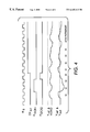
- FIG. 4 is a set of comparative, simultaneous waveforms indicating the operation of the different switches in the circuit of FIG. 3, during the time in which dark photosensors, such as dark photosensor D 2 and dark photosensor D 3 of dark photosensors 110 , are used to set the offset for the readout of active photosensor 102 for each scan.
- Waveform ⁇ s at the top of FIG. 4, shows the clock pulses by which video signals from dark photosensors 110 or active photosensors 102 are read out on video line 108 .
- the waveforms ⁇ DCR1 and ⁇ DCR2 in FIG. 4 illustrate the operation of the corresponding switches in the circuit of FIG. 3, such as the switch in RC circuit 140 associated with switching means 144 and bypass switch 148 .
- DCR stands for “DC restore.”
- ⁇ DCR1 goes high, which connects RC circuit 140 to video line 108 , and activates bypass switch 148 , which causes the signal on video line 108 to bypass correction capacitor 130 .
- ⁇ DCR1 goes high, which connects RC circuit 140 to video line 108 , and activates bypass switch 148 , which causes the signal on video line 108 to bypass correction capacitor 130 .
- ⁇ DCR1 goes high, which connects RC circuit 140 to video line 108 , and activates bypass switch 148 , which causes the signal on video line 108 to bypass correction capacitor 130 .
- the RC circuit 140 functions as an averaging circuit which samples the video from both the dark photosensor D 2 and dark photosensor D 3 with every scan on video line 108 .
- the values of R and C of the RC circuit 140 should be set so that samples of the video signals from dark photosensor D 2 and dark photosensor D 3 over a relatively large number of scans are accumulated.
- R and C should provide a time constant by which the effect of numerous scans of dark photosensors D 2 and D 3 loaded onto the RC circuit 140 cause the RC circuit 140 to maintain a running average of the outputs of dark photosensors D 2 and D 3 over a large number of scanlines.
- the value of RC should be set equal to 100 times the duration of the sample clock with each scan.
- the RC should be chosen to sample at least 10 scanlines, and preferably about 100 scanlines, in order to obtain its average dark photosensor signal.
- RC circuit 140 thus has the effect, by its accumulation of sample charges over as many as 100 scanlines, of averaging put the random thermal noise of the individual dark photosensors.
- the noise on the dark photosensors will be reduced by a factor of (n ⁇ m) 0.5 , where n is the number of scanlines averaged, and m is the number of dark photosensors averaged with each scanline.
- the charge from RC circuit 140 is connected, through line 142 , to video line 108 , so that the charge on RC circuit 140 can be used to affect correction capacitor 130 on one side while V REF is applied to correction capacitor 130 on the other side.
- the charge on RC circuit 140 which as mentioned above is representative of an average of a large number of samples from dark photosensors D 2 and D 3 over many scanlines, is used to set correction capacitor 130 prefatory to the readout of the active photosensors on video line 108 .
- correction capacitor 130 in the FIG. 3 embodiment is the same as with the FIG. 2 embodiment described above, with the significant difference that, whereas the FIG. 2 embodiment merely used a single reading of a single dark photosensor to set the charge on correction capacitor 130 , the circuit of FIG. 3 uses an average reading of two of dark photosensors sampled many times, this average reading being maintained by RC circuit 140 .
- offset correction from the perspective of the photosensor circuitry is to some extent at cross-purposes with offset correction with regard to the downstream image-processing circuitry.
- this problem is addressed by providing, with each scanline of reading out dark photosensor signals and active photosensor signals, two readings from the dark photosensors: in the first reading of signals from the dark photosensors, the correction capacitor 130 is bypassed by bypass switch 148 and the dark signals are thus transferred to the averaging circuit 140 ; in the second reading of the dark pixels, the same dark photosensor signals are read out again, with this time the correction capacitor 130 not bypassed by bypass switch 148 ; instead of the dark photosensor signals being sent to averaging circuit 140 , an “output enable,” or OE, transistor switch 150 is activated so that the dark photosensor signals are sent downstream to video circuitry.
- an “output enable,” or OE transistor switch 150 is activated so that the dark photosensor signals are sent downstream to video circuitry.
- the averaged dark photosensor signals come from dark photosensors D 2 and D 3 (with reference to FIG. 1 above). As can be seen in the output signals at the bottom of the clocking diagram, with every scanline, the dark photosensors are read out twice before the active pixels (such as 102 in FIG. 1) read out to the video line 108 .
- the switch DCR 1 is made high for the duration of readouts of: dark photosensors D 2 and D 3 :
- this DCR 1 going high causes both a bypass of the video signals around correction capacitor 130 , and a connection of the dark photosensor signals to averaging circuit 140 .
- DCR 2 goes high:
- DCR 2 going high connects the potential on the capacitor of averaging circuit 140 to the video line 108 , and also causes a clamping of a reference voltage V REF from source 132 onto correction capacitor 130 .
- this combination of readout of the potential from the averaging circuit 140 with the reference voltage 132 creates a correction potential on correction capacitor 130 , which in turn is used to correct signals which will be subsequently output from active photosensors on video line 108 .
- the line OE INT is low.
- transistor 150 effectively cuts off the circuit of FIG. 3 from downstream circuitry, so that the dark photosensor signals on video line 108 are sent only to the averaging circuit 140 .
- both DCR 1 and DCR 2 are low, while the signal on OE INT (output enable transistor 150 ) is high.
- this condition means that the dark photosensor signals read out on video line 108 pass through correction capacitor 130 , and are not sent to averaging circuit 140 but through output enable transistor 150 to downstream video circuitry. This particular cycle of dark-photosensor readouts is used for the benefit of calibrating downstream video circuitry.
- FIG. 4 shows the first D 2 and D 3 readout in “Vout” is not DCR restored. If the first D 2 & D 3 levels were included in the video sent downstream it could significantly add to the dark nonuniformity of the video and the range needed for pixel to pixel dark level correction.
- FIGS. 5 and 6 are simplified diagrams showing various embodiments of circuits which carryout the double readout of the dark photosensors.
- like numbers such as shown in FIG. 1 above represent like elements.
- the arrangement of FIG. 5 shows a modification of the shift register relationship shown in FIG. 1, where there is provided, along shift register line 112 , two sets of shift register stages for each of the dark photosensors 110 .
- the shift register input to each dark photosensor 110 is connected through an OR gate 200 to two separate shift register stages 114 .
- FIG. 6 shows another possible implementation to enable the double readout system of the present invention.
- the dark photodiodes D 1 -D 4 share the video line 108 with the active photosensors 102 , but the dark photosensors 110 are controlled by a separate, small shift register, forming a shift register line 113 , which is distinct from the shift register line 112 used for the active photosensors 102 .
- the dark photosensors 110 can be read out essentially independently of the readout of the active photosensors 102 .
Landscapes
- Engineering & Computer Science (AREA)
- Multimedia (AREA)
- Signal Processing (AREA)
- Facsimile Scanning Arrangements (AREA)
- Transforming Light Signals Into Electric Signals (AREA)
Abstract
Description
Claims (20)
Priority Applications (1)
| Application Number | Priority Date | Filing Date | Title |
|---|---|---|---|
| US09/138,941 US6445413B1 (en) | 1998-08-24 | 1998-08-24 | System for determining a video offset from dark photosensors in an image sensor array |
Applications Claiming Priority (1)
| Application Number | Priority Date | Filing Date | Title |
|---|---|---|---|
| US09/138,941 US6445413B1 (en) | 1998-08-24 | 1998-08-24 | System for determining a video offset from dark photosensors in an image sensor array |
Publications (1)
| Publication Number | Publication Date |
|---|---|
| US6445413B1 true US6445413B1 (en) | 2002-09-03 |
Family
ID=22484353
Family Applications (1)
| Application Number | Title | Priority Date | Filing Date |
|---|---|---|---|
| US09/138,941 Expired - Lifetime US6445413B1 (en) | 1998-08-24 | 1998-08-24 | System for determining a video offset from dark photosensors in an image sensor array |
Country Status (1)
| Country | Link |
|---|---|
| US (1) | US6445413B1 (en) |
Cited By (12)
| Publication number | Priority date | Publication date | Assignee | Title |
|---|---|---|---|---|
| US20020101522A1 (en) * | 2001-01-30 | 2002-08-01 | Xerox Corporation | Combined multiplexing and offset correction for an image sensor array |
| US20030020818A1 (en) * | 2001-07-25 | 2003-01-30 | Eastman Kodak Company | Median-based dark level acquisition for a frame rate clamp |
| US20030103152A1 (en) * | 2000-09-26 | 2003-06-05 | Rohm Co., Ltd. | Image reading device |
| US6744526B2 (en) * | 2001-02-09 | 2004-06-01 | Eastman Kodak Company | Image sensor having black pixels disposed in a spaced-apart relationship from the active pixels |
| US20050200732A1 (en) * | 2004-03-15 | 2005-09-15 | Boon Keat Tan | System and method for canceling dark photocurrent in a color sensor circuit |
| US20050206764A1 (en) * | 1998-02-20 | 2005-09-22 | Canon Kabushiki Kaisha | Photoelectric converter and radiation reader |
| US20060197858A1 (en) * | 1998-10-14 | 2006-09-07 | Matsushita Electric Industrial Co., Ltd. | Amplifying solid-state imaging device, and method for driving the same |
| US20070216789A1 (en) * | 2006-03-15 | 2007-09-20 | Honeywell International, Inc. | System and apparatus for high dynamic range sensor |
| US20080291290A1 (en) * | 2007-05-21 | 2008-11-27 | Canon Kabushiki Kaisha | Imaging apparatus and processing method thereof |
| US20090102954A1 (en) * | 2007-10-23 | 2009-04-23 | Xerox Corporation | Multiplexing and offset correction system for an image sensor array |
| US7564489B1 (en) * | 2005-02-18 | 2009-07-21 | Crosstek Capital, LLC | Method for reducing row noise with dark pixel data |
| US8310577B1 (en) | 1999-08-19 | 2012-11-13 | Youliza, Gehts B.V. Limited Liability Company | Method and apparatus for color compensation |
Citations (10)
| Publication number | Priority date | Publication date | Assignee | Title |
|---|---|---|---|---|
| US4649430A (en) * | 1985-08-27 | 1987-03-10 | Texas Instruments, Incorporated | CCD imager with many dummy pixels |
| US5047861A (en) * | 1990-07-31 | 1991-09-10 | Eastman Kodak Company | Method and apparatus for pixel non-uniformity correction |
| US5162735A (en) * | 1991-02-28 | 1992-11-10 | Nec Corporation | Operational amplifier circuit with improved gain of feedback loop |
| US5231503A (en) * | 1990-07-26 | 1993-07-27 | Nippon Steel Corporation | Image sensor apparatus with noise cancellation circuitry |
| US5268765A (en) * | 1991-04-15 | 1993-12-07 | Mitsubishi Denki Kabushiki Kaisha | Image sensor and image sensor chips therefor including dummy photocells and internal discharge switches |
| US5633679A (en) * | 1995-05-19 | 1997-05-27 | Xerox Corporation | Photosensitive chip having transfer circuits which compensate for shielded test photosensors |
| US5654755A (en) * | 1996-01-05 | 1997-08-05 | Xerox Corporation | System for determining a video offset from dark photosensors in an image sensor array |
| US6118115A (en) * | 1997-07-18 | 2000-09-12 | Canon Kabushiki Kaisha | Photoelectric conversion apparatus |
| US6130712A (en) * | 1996-06-11 | 2000-10-10 | Canon Kabushiki Kaisha | Eliminating the influence of random noise produced by an optical black pixel on a reference output |
| US6141045A (en) * | 1997-09-22 | 2000-10-31 | Xerox Corporation | Method for detecting defective photosensor circuits in a photosensor array |
-
1998
- 1998-08-24 US US09/138,941 patent/US6445413B1/en not_active Expired - Lifetime
Patent Citations (10)
| Publication number | Priority date | Publication date | Assignee | Title |
|---|---|---|---|---|
| US4649430A (en) * | 1985-08-27 | 1987-03-10 | Texas Instruments, Incorporated | CCD imager with many dummy pixels |
| US5231503A (en) * | 1990-07-26 | 1993-07-27 | Nippon Steel Corporation | Image sensor apparatus with noise cancellation circuitry |
| US5047861A (en) * | 1990-07-31 | 1991-09-10 | Eastman Kodak Company | Method and apparatus for pixel non-uniformity correction |
| US5162735A (en) * | 1991-02-28 | 1992-11-10 | Nec Corporation | Operational amplifier circuit with improved gain of feedback loop |
| US5268765A (en) * | 1991-04-15 | 1993-12-07 | Mitsubishi Denki Kabushiki Kaisha | Image sensor and image sensor chips therefor including dummy photocells and internal discharge switches |
| US5633679A (en) * | 1995-05-19 | 1997-05-27 | Xerox Corporation | Photosensitive chip having transfer circuits which compensate for shielded test photosensors |
| US5654755A (en) * | 1996-01-05 | 1997-08-05 | Xerox Corporation | System for determining a video offset from dark photosensors in an image sensor array |
| US6130712A (en) * | 1996-06-11 | 2000-10-10 | Canon Kabushiki Kaisha | Eliminating the influence of random noise produced by an optical black pixel on a reference output |
| US6118115A (en) * | 1997-07-18 | 2000-09-12 | Canon Kabushiki Kaisha | Photoelectric conversion apparatus |
| US6141045A (en) * | 1997-09-22 | 2000-10-31 | Xerox Corporation | Method for detecting defective photosensor circuits in a photosensor array |
Cited By (28)
| Publication number | Priority date | Publication date | Assignee | Title |
|---|---|---|---|---|
| US20050206764A1 (en) * | 1998-02-20 | 2005-09-22 | Canon Kabushiki Kaisha | Photoelectric converter and radiation reader |
| US7724295B2 (en) * | 1998-02-20 | 2010-05-25 | Canon Kabushiki Kaisha | Photoelectric converter and radiation reader |
| US20110007197A1 (en) * | 1998-10-14 | 2011-01-13 | Panasonic Corporation | Amplifying solid-state imaging device, and method for driving the same |
| US7532243B2 (en) * | 1998-10-14 | 2009-05-12 | Panasonic Corporation | Amplifying solid-state imaging device, and method for driving the same |
| US20090207289A1 (en) * | 1998-10-14 | 2009-08-20 | Panasonic Corporation | Amplifying solid-state imaging device, and method for driving the same |
| US8218048B2 (en) | 1998-10-14 | 2012-07-10 | Panasonic Corporation | Amplifying solid-state imaging device, and method for driving the same |
| US7821556B2 (en) | 1998-10-14 | 2010-10-26 | Panasonic Corporation | Amplifying solid-state imaging device, and method for driving the same |
| US20060197858A1 (en) * | 1998-10-14 | 2006-09-07 | Matsushita Electric Industrial Co., Ltd. | Amplifying solid-state imaging device, and method for driving the same |
| US8310577B1 (en) | 1999-08-19 | 2012-11-13 | Youliza, Gehts B.V. Limited Liability Company | Method and apparatus for color compensation |
| US20030103152A1 (en) * | 2000-09-26 | 2003-06-05 | Rohm Co., Ltd. | Image reading device |
| US7298403B2 (en) * | 2000-09-26 | 2007-11-20 | Rohm Co., Ltd. | Image reading device |
| US20020101522A1 (en) * | 2001-01-30 | 2002-08-01 | Xerox Corporation | Combined multiplexing and offset correction for an image sensor array |
| US6853402B2 (en) * | 2001-01-30 | 2005-02-08 | Xerox Corporation | Combined multiplexing and offset correction for an image sensor array |
| US6744526B2 (en) * | 2001-02-09 | 2004-06-01 | Eastman Kodak Company | Image sensor having black pixels disposed in a spaced-apart relationship from the active pixels |
| US6909460B2 (en) * | 2001-07-25 | 2005-06-21 | Eastman Kodak Company | Median-based dark level acquisition for a frame rate clamp |
| US20030020818A1 (en) * | 2001-07-25 | 2003-01-30 | Eastman Kodak Company | Median-based dark level acquisition for a frame rate clamp |
| US20050200732A1 (en) * | 2004-03-15 | 2005-09-15 | Boon Keat Tan | System and method for canceling dark photocurrent in a color sensor circuit |
| US7773134B2 (en) * | 2004-03-15 | 2010-08-10 | Avago Technologies Ecbu Ip (Singapore) Pte. Ltd. | System and method for canceling dark photocurrent in a color sensor circuit |
| US7889249B2 (en) | 2004-03-15 | 2011-02-15 | Avago Technologies Ecbu Ip (Singapore) Pte. Ltd. | System and method for canceling dark photocurrent in a color sensor circuit |
| US7982784B2 (en) | 2005-02-18 | 2011-07-19 | Crosstek Capital, LLC | Method for reducing row noise with dark pixel data |
| US20100039537A1 (en) * | 2005-02-18 | 2010-02-18 | Crosstek Capital, LLC | Method for reducing row noise with dark pixel data |
| US7564489B1 (en) * | 2005-02-18 | 2009-07-21 | Crosstek Capital, LLC | Method for reducing row noise with dark pixel data |
| US20070216789A1 (en) * | 2006-03-15 | 2007-09-20 | Honeywell International, Inc. | System and apparatus for high dynamic range sensor |
| US7750960B2 (en) * | 2006-03-15 | 2010-07-06 | Honeywell International Inc. | System and apparatus for high dynamic range sensor |
| US20080291290A1 (en) * | 2007-05-21 | 2008-11-27 | Canon Kabushiki Kaisha | Imaging apparatus and processing method thereof |
| US7999866B2 (en) * | 2007-05-21 | 2011-08-16 | Canon Kabushiki Kaisha | Imaging apparatus and processing method thereof |
| US20090102954A1 (en) * | 2007-10-23 | 2009-04-23 | Xerox Corporation | Multiplexing and offset correction system for an image sensor array |
| US7893977B2 (en) | 2007-10-23 | 2011-02-22 | Xerox Corporation | Multiplexing and offset correction system for an image sensor array |
Similar Documents
| Publication | Publication Date | Title |
|---|---|---|
| US5153421A (en) | Architecture for analog and digital image sensor arrays | |
| US5654755A (en) | System for determining a video offset from dark photosensors in an image sensor array | |
| EP2378764B1 (en) | A camera | |
| US5920345A (en) | CMOS image sensor with improved fill factor | |
| US6704050B1 (en) | Active-pixel image sensing device with linear mode voltage to current conversion | |
| US5969758A (en) | DC offset and gain correction for CMOS image sensor | |
| US5493423A (en) | Resettable pixel amplifier for an image sensor array | |
| US20060102827A1 (en) | Solid-state imaging device | |
| US6445413B1 (en) | System for determining a video offset from dark photosensors in an image sensor array | |
| US6710803B1 (en) | Image sensor and method for driving the same | |
| KR100638196B1 (en) | Cmos image sensor which reduced noise caused by charge pump operation | |
| US5633679A (en) | Photosensitive chip having transfer circuits which compensate for shielded test photosensors | |
| US6950132B1 (en) | Image sensor and method for driving an image sensor for reducing fixed pattern noise | |
| US6853402B2 (en) | Combined multiplexing and offset correction for an image sensor array | |
| KR20010070481A (en) | Active pixel sensor with improved reference signal | |
| US7327500B2 (en) | Image inputting apparatus | |
| US20060291008A1 (en) | System for adjusting a reference voltage in a photosensor chip | |
| JPH0730820A (en) | Solid-state image pickup device | |
| US20090015692A1 (en) | Methods, systems, and devices for offset compensation in cmos imagers | |
| JP2856940B2 (en) | Image reading device | |
| US6657662B1 (en) | System for resetting the video offset from dark photosensors in an image sensor array | |
| JP3332026B2 (en) | Photoelectric conversion device | |
| EP0683602B1 (en) | Method and apparatus for a low noise, charge coupled device | |
| US6259087B1 (en) | Calibration apparatus for multi-element sensor | |
| JPH11122538A (en) | Defective pixel correction device |
Legal Events
| Date | Code | Title | Description |
|---|---|---|---|
| AS | Assignment |
Owner name: XEROX CORPORATION, CONNECTICUT Free format text: ASSIGNMENT OF ASSIGNORS INTEREST;ASSIGNORS:HOSIER, PAUL A.;TEWINKLE, SCOTT L.;REEL/FRAME:009413/0040 Effective date: 19980814 |
|
| AS | Assignment |
Owner name: BANK ONE, NA, AS ADMINISTRATIVE AGENT, ILLINOIS Free format text: SECURITY AGREEMENT;ASSIGNOR:XEROX CORPORATION;REEL/FRAME:013111/0001 Effective date: 20020621 Owner name: BANK ONE, NA, AS ADMINISTRATIVE AGENT,ILLINOIS Free format text: SECURITY AGREEMENT;ASSIGNOR:XEROX CORPORATION;REEL/FRAME:013111/0001 Effective date: 20020621 |
|
| STCF | Information on status: patent grant |
Free format text: PATENTED CASE |
|
| AS | Assignment |
Owner name: JPMORGAN CHASE BANK, AS COLLATERAL AGENT, TEXAS Free format text: SECURITY AGREEMENT;ASSIGNOR:XEROX CORPORATION;REEL/FRAME:015134/0476 Effective date: 20030625 Owner name: JPMORGAN CHASE BANK, AS COLLATERAL AGENT,TEXAS Free format text: SECURITY AGREEMENT;ASSIGNOR:XEROX CORPORATION;REEL/FRAME:015134/0476 Effective date: 20030625 |
|
| FPAY | Fee payment |
Year of fee payment: 4 |
|
| FPAY | Fee payment |
Year of fee payment: 8 |
|
| FPAY | Fee payment |
Year of fee payment: 12 |
|
| AS | Assignment |
Owner name: XEROX CORPORATION, NEW YORK Free format text: RELEASE BY SECURED PARTY;ASSIGNOR:BANK ONE, NA;REEL/FRAME:034781/0055 Effective date: 20030625 |
|
| AS | Assignment |
Owner name: XEROX CORPORATION, NEW YORK Free format text: RELEASE BY SECURED PARTY;ASSIGNOR:JPMORGAN CHASE BANK, N.A.;REEL/FRAME:034781/0444 Effective date: 20061204 |
|
| AS | Assignment |
Owner name: XEROX CORPORATION, CONNECTICUT Free format text: RELEASE BY SECURED PARTY;ASSIGNOR:JPMORGAN CHASE BANK, N.A. AS SUCCESSOR-IN-INTEREST ADMINISTRATIVE AGENT AND COLLATERAL AGENT TO BANK ONE, N.A.;REEL/FRAME:061388/0388 Effective date: 20220822 Owner name: XEROX CORPORATION, CONNECTICUT Free format text: RELEASE BY SECURED PARTY;ASSIGNOR:JPMORGAN CHASE BANK, N.A. AS SUCCESSOR-IN-INTEREST ADMINISTRATIVE AGENT AND COLLATERAL AGENT TO JPMORGAN CHASE BANK;REEL/FRAME:066728/0193 Effective date: 20220822 |