US6441396B1 - In-line electrical monitor for measuring mechanical stress at the device level on a semiconductor wafer - Google Patents
In-line electrical monitor for measuring mechanical stress at the device level on a semiconductor wafer Download PDFInfo
- Publication number
- US6441396B1 US6441396B1 US09/695,038 US69503800A US6441396B1 US 6441396 B1 US6441396 B1 US 6441396B1 US 69503800 A US69503800 A US 69503800A US 6441396 B1 US6441396 B1 US 6441396B1
- Authority
- US
- United States
- Prior art keywords
- diode
- stress
- well
- diode structure
- isolation
- Prior art date
- Legal status (The legal status is an assumption and is not a legal conclusion. Google has not performed a legal analysis and makes no representation as to the accuracy of the status listed.)
- Expired - Fee Related, expires
Links
- 239000004065 semiconductor Substances 0.000 title claims abstract description 39
- 238000012544 monitoring process Methods 0.000 claims abstract description 29
- 238000002955 isolation Methods 0.000 claims description 53
- 238000009792 diffusion process Methods 0.000 claims description 35
- 238000005259 measurement Methods 0.000 claims description 32
- 239000000758 substrate Substances 0.000 claims description 13
- 239000000463 material Substances 0.000 claims description 10
- 239000003989 dielectric material Substances 0.000 claims description 8
- 230000003071 parasitic effect Effects 0.000 claims description 7
- 230000001939 inductive effect Effects 0.000 claims description 4
- 238000012806 monitoring device Methods 0.000 claims description 3
- 238000000034 method Methods 0.000 abstract description 33
- 230000008569 process Effects 0.000 abstract description 18
- 238000004519 manufacturing process Methods 0.000 abstract description 17
- 230000008859 change Effects 0.000 abstract description 2
- 230000035882 stress Effects 0.000 description 116
- 235000012431 wafers Nutrition 0.000 description 25
- 239000013078 crystal Substances 0.000 description 15
- 230000000694 effects Effects 0.000 description 15
- XUIMIQQOPSSXEZ-UHFFFAOYSA-N Silicon Chemical compound [Si] XUIMIQQOPSSXEZ-UHFFFAOYSA-N 0.000 description 12
- 229910052710 silicon Inorganic materials 0.000 description 12
- 239000010703 silicon Substances 0.000 description 12
- 238000013461 design Methods 0.000 description 8
- FVBUAEGBCNSCDD-UHFFFAOYSA-N silicide(4-) Chemical compound [Si-4] FVBUAEGBCNSCDD-UHFFFAOYSA-N 0.000 description 5
- 238000005516 engineering process Methods 0.000 description 4
- 238000012360 testing method Methods 0.000 description 4
- 230000015572 biosynthetic process Effects 0.000 description 3
- 239000002019 doping agent Substances 0.000 description 3
- 230000001965 increasing effect Effects 0.000 description 3
- 229910044991 metal oxide Inorganic materials 0.000 description 3
- 150000004706 metal oxides Chemical class 0.000 description 3
- 150000004767 nitrides Chemical class 0.000 description 3
- 229910021332 silicide Inorganic materials 0.000 description 3
- ZOXJGFHDIHLPTG-UHFFFAOYSA-N Boron Chemical compound [B] ZOXJGFHDIHLPTG-UHFFFAOYSA-N 0.000 description 2
- 230000008901 benefit Effects 0.000 description 2
- 229910052796 boron Inorganic materials 0.000 description 2
- 238000004364 calculation method Methods 0.000 description 2
- 230000007547 defect Effects 0.000 description 2
- 238000000280 densification Methods 0.000 description 2
- 230000005669 field effect Effects 0.000 description 2
- 238000005468 ion implantation Methods 0.000 description 2
- 238000012986 modification Methods 0.000 description 2
- 230000004048 modification Effects 0.000 description 2
- 230000003647 oxidation Effects 0.000 description 2
- 238000007254 oxidation reaction Methods 0.000 description 2
- 239000000047 product Substances 0.000 description 2
- 238000005389 semiconductor device fabrication Methods 0.000 description 2
- 230000035945 sensitivity Effects 0.000 description 2
- 239000007787 solid Substances 0.000 description 2
- 241000293849 Cordylanthus Species 0.000 description 1
- 230000004913 activation Effects 0.000 description 1
- 230000002547 anomalous effect Effects 0.000 description 1
- 229910052785 arsenic Inorganic materials 0.000 description 1
- RQNWIZPPADIBDY-UHFFFAOYSA-N arsenic atom Chemical compound [As] RQNWIZPPADIBDY-UHFFFAOYSA-N 0.000 description 1
- 230000009286 beneficial effect Effects 0.000 description 1
- 239000006227 byproduct Substances 0.000 description 1
- 239000003990 capacitor Substances 0.000 description 1
- 238000012512 characterization method Methods 0.000 description 1
- 230000000295 complement effect Effects 0.000 description 1
- 238000010276 construction Methods 0.000 description 1
- 230000007423 decrease Effects 0.000 description 1
- 238000001514 detection method Methods 0.000 description 1
- 230000009429 distress Effects 0.000 description 1
- 230000005684 electric field Effects 0.000 description 1
- 230000002706 hydrostatic effect Effects 0.000 description 1
- 239000007943 implant Substances 0.000 description 1
- 230000010354 integration Effects 0.000 description 1
- 238000012886 linear function Methods 0.000 description 1
- 238000002161 passivation Methods 0.000 description 1
- 230000000704 physical effect Effects 0.000 description 1
- 229910021420 polycrystalline silicon Inorganic materials 0.000 description 1
- 229920005591 polysilicon Polymers 0.000 description 1
- 230000009467 reduction Effects 0.000 description 1
- 239000000523 sample Substances 0.000 description 1
- 238000005070 sampling Methods 0.000 description 1
- LIVNPJMFVYWSIS-UHFFFAOYSA-N silicon monoxide Chemical class [Si-]#[O+] LIVNPJMFVYWSIS-UHFFFAOYSA-N 0.000 description 1
- 229910052814 silicon oxide Inorganic materials 0.000 description 1
- 125000006850 spacer group Chemical group 0.000 description 1
Images


Classifications
-
- H—ELECTRICITY
- H01—ELECTRIC ELEMENTS
- H01L—SEMICONDUCTOR DEVICES NOT COVERED BY CLASS H10
- H01L23/00—Details of semiconductor or other solid state devices
- H01L23/544—Marks applied to semiconductor devices or parts, e.g. registration marks, alignment structures, wafer maps
-
- H—ELECTRICITY
- H01—ELECTRIC ELEMENTS
- H01L—SEMICONDUCTOR DEVICES NOT COVERED BY CLASS H10
- H01L21/00—Processes or apparatus adapted for the manufacture or treatment of semiconductor or solid state devices or of parts thereof
- H01L21/67—Apparatus specially adapted for handling semiconductor or electric solid state devices during manufacture or treatment thereof; Apparatus specially adapted for handling wafers during manufacture or treatment of semiconductor or electric solid state devices or components ; Apparatus not specifically provided for elsewhere
- H01L21/67005—Apparatus not specifically provided for elsewhere
- H01L21/67242—Apparatus for monitoring, sorting or marking
- H01L21/67288—Monitoring of warpage, curvature, damage, defects or the like
-
- H—ELECTRICITY
- H01—ELECTRIC ELEMENTS
- H01L—SEMICONDUCTOR DEVICES NOT COVERED BY CLASS H10
- H01L22/00—Testing or measuring during manufacture or treatment; Reliability measurements, i.e. testing of parts without further processing to modify the parts as such; Structural arrangements therefor
- H01L22/30—Structural arrangements specially adapted for testing or measuring during manufacture or treatment, or specially adapted for reliability measurements
- H01L22/34—Circuits for electrically characterising or monitoring manufacturing processes, e. g. whole test die, wafers filled with test structures, on-board-devices incorporated on each die, process control monitors or pad structures thereof, devices in scribe line
-
- H—ELECTRICITY
- H01—ELECTRIC ELEMENTS
- H01L—SEMICONDUCTOR DEVICES NOT COVERED BY CLASS H10
- H01L29/00—Semiconductor devices adapted for rectifying, amplifying, oscillating or switching, or capacitors or resistors with at least one potential-jump barrier or surface barrier, e.g. PN junction depletion layer or carrier concentration layer; Details of semiconductor bodies or of electrodes thereof ; Multistep manufacturing processes therefor
- H01L29/66—Types of semiconductor device ; Multistep manufacturing processes therefor
- H01L29/68—Types of semiconductor device ; Multistep manufacturing processes therefor controllable by only the electric current supplied, or only the electric potential applied, to an electrode which does not carry the current to be rectified, amplified or switched
- H01L29/76—Unipolar devices, e.g. field effect transistors
- H01L29/772—Field effect transistors
- H01L29/78—Field effect transistors with field effect produced by an insulated gate
- H01L29/7842—Field effect transistors with field effect produced by an insulated gate means for exerting mechanical stress on the crystal lattice of the channel region, e.g. using a flexible substrate
-
- G—PHYSICS
- G01—MEASURING; TESTING
- G01N—INVESTIGATING OR ANALYSING MATERIALS BY DETERMINING THEIR CHEMICAL OR PHYSICAL PROPERTIES
- G01N2203/00—Investigating strength properties of solid materials by application of mechanical stress
- G01N2203/0014—Type of force applied
- G01N2203/0016—Tensile or compressive
-
- G—PHYSICS
- G01—MEASURING; TESTING
- G01N—INVESTIGATING OR ANALYSING MATERIALS BY DETERMINING THEIR CHEMICAL OR PHYSICAL PROPERTIES
- G01N2203/00—Investigating strength properties of solid materials by application of mechanical stress
- G01N2203/0014—Type of force applied
- G01N2203/0025—Shearing
-
- G—PHYSICS
- G01—MEASURING; TESTING
- G01N—INVESTIGATING OR ANALYSING MATERIALS BY DETERMINING THEIR CHEMICAL OR PHYSICAL PROPERTIES
- G01N2203/00—Investigating strength properties of solid materials by application of mechanical stress
- G01N2203/02—Details not specific for a particular testing method
- G01N2203/026—Specifications of the specimen
- G01N2203/0286—Miniature specimen; Testing on microregions of a specimen
-
- G—PHYSICS
- G01—MEASURING; TESTING
- G01N—INVESTIGATING OR ANALYSING MATERIALS BY DETERMINING THEIR CHEMICAL OR PHYSICAL PROPERTIES
- G01N2203/00—Investigating strength properties of solid materials by application of mechanical stress
- G01N2203/02—Details not specific for a particular testing method
- G01N2203/06—Indicating or recording means; Sensing means
- G01N2203/0617—Electrical or magnetic indicating, recording or sensing means
-
- H—ELECTRICITY
- H01—ELECTRIC ELEMENTS
- H01L—SEMICONDUCTOR DEVICES NOT COVERED BY CLASS H10
- H01L22/00—Testing or measuring during manufacture or treatment; Reliability measurements, i.e. testing of parts without further processing to modify the parts as such; Structural arrangements therefor
- H01L22/10—Measuring as part of the manufacturing process
- H01L22/12—Measuring as part of the manufacturing process for structural parameters, e.g. thickness, line width, refractive index, temperature, warp, bond strength, defects, optical inspection, electrical measurement of structural dimensions, metallurgic measurement of diffusions
-
- H—ELECTRICITY
- H01—ELECTRIC ELEMENTS
- H01L—SEMICONDUCTOR DEVICES NOT COVERED BY CLASS H10
- H01L2223/00—Details relating to semiconductor or other solid state devices covered by the group H01L23/00
- H01L2223/544—Marks applied to semiconductor devices or parts
- H01L2223/54453—Marks applied to semiconductor devices or parts for use prior to dicing
-
- H—ELECTRICITY
- H01—ELECTRIC ELEMENTS
- H01L—SEMICONDUCTOR DEVICES NOT COVERED BY CLASS H10
- H01L2924/00—Indexing scheme for arrangements or methods for connecting or disconnecting semiconductor or solid-state bodies as covered by H01L24/00
- H01L2924/0001—Technical content checked by a classifier
- H01L2924/0002—Not covered by any one of groups H01L24/00, H01L24/00 and H01L2224/00
Definitions
- the present invention relates generally to the field of semiconductor device formation, and more specifically to a method and apparatus, integrated with said devices, for measuring mechanical stress induced in those devices.
- Such stress is either induced by the intrinsic fabrication process of the devices, or by extrinsic means, such as a vacuum chuck used during electrical tests.
- the method is particularly useful for measuring mechanical stress on semiconductor devices induced by the process of formation of either dielectric-filled isolation trenches or by semi-recessed oxide (SROX) isolation regions, which abut the devices of interest.
- SROX semi-recessed oxide
- Dielectric-filled trench isolation is a common method of electrically isolating solid state silicon devices. It is especially common in complementary metal-oxide semiconductor (“CMOS”) technology as an alternative to back-biased isolation diffusion techniques used in negative-channel metal-oxide semiconductor (“NMOS”), positive-channel metal-oxide semiconductor (“PMOS”), or bipolar technologies.
- CMOS complementary metal-oxide semiconductor
- NMOS negative-channel metal-oxide semiconductor
- PMOS positive-channel metal-oxide semiconductor
- bipolar technologies bipolar technologies.
- dielectric-filled trench isolation is difficult to implement in CMOS technology.
- trench isolation as used in semiconductor structures causes the semiconductor structure to behave much the same as a piezoresistive device (i.e., a device whose resistance changes with the applied stress), and the effects of induced mechanical stress can modulate the nominal electrical behavior of a properly designed device, or array of such devices, for the purpose of measuring the induced stress. It is to be noted that extrinsically generated stress will also modulate device behavior and that this stress, too, can effectively be measured.
- VLSI very large-scale integration
- the invention disclosed herein presents a method and related structures that enable monitoring of stress acting upon a semiconductor structure.
- a method and apparatus for measuring the stress at microscopic levels is disclosed.
- the invention relies on the dimensional dependence between the width of a device and the inherent resistivity in the device.
- the present invention discloses a method and apparatus used to measure the stress at a sub-chip (i.e., device and chip) level with resolution of stress effects on electrical conduction.
- the present invention permits obtaining data on the position dependence of stress effects on devices, including orientational effects on a semiconductor wafer or substrate used in production of VLSI devices and circuits.
- the present invention also allows monitoring of the dependence of stress on device size, particularly via wide-to-narrow diode behavior.
- the present invention provides a structure for measuring stress in a semiconductor device comprising: a pn diode formed on the surface of a semiconductor device, said diode being bounded by a first shallow trench isolation region having predetermined dimensions; a diffusion region formed on the surface of the wafer, said diffusion region being bound by a second shallow trench isolation region having the same dimensions as the first shallow trench region; and contacts formed on said diode and diffusion region for passing current through the diode and through said diffusion region.
- the present invention additionally provides a method of monitoring stress in a silicon substrate comprising the steps of: forming a first device comprising a pn diode in a first n-well region of a p-well formed in said silicon substrate, said pn diode having a geometry defined by a dielectric-filled trench; forming a second device comprising a p-type diffusion region in a second n-well region formed in said p-well region of said silicon substrate, said second n-well region having a geometry substantially the same as the geometry of said first n-well region and defined by a dielectric-filled trench; subtracting a first current measurement through said second device from a first current measurement from said first device.
- the present invention further provides a method of using a stress monitor structure formed in a semiconductor wafer comprising the steps of: applying a current to the stress monitor structure; measuring a resultant bias voltage induced in the stress monitor structure by the current; comparing the stress-induced resultant bias voltage to a reference non-stress-induced bias voltage; and determining the amount of stress-induced electrical parameter variations in the semiconductor wafer.
- the present invention also provides a stress monitoring unit comprising: a semiconductor material forming a base structure, said base structure containing a diode structure and a non-diode structure; said diode structure formed in the semiconductor material; said non-diode structure including a plurality of isolation trenches surrounding the diode structure, said isolation trenches being filled with a dielectric material; a system for applying an electrical potential across the diode structure, thereby inducing a diode current to flow through the diode structure; a system for measuring the diode current; and a system for translating the amount of diode current measured into dimensional units representing the stress on the base structure.
- the present invention also discloses a stress monitoring set comprising: at least one pair of diode devices, or an array or plurality of diode devices, said pair consisting of a first device and a second device, wherein said first device is a reference device, and said second device (or array of secondary devices) is (are) a measurement device.
- the present invention additionally discloses a stress monitoring system for monitoring mechanical stress in a semiconductor substrate containing trench isolation regions comprising: a semiconductor material forming a base structure, said base structure containing a diode structure and a non-diode structure; said diode structure formed in the semiconductor material; said non-diode structure including a plurality of isolation trenches surrounding the diode structure, said isolation trenches being filled with a dielectric material; a system for applying an electrical potential across the diode structure, thereby inducing a diode current to flow through the diode structure; a system for measuring the diode current; and a system for translating the amount of diode current measured into dimensional units representing the stress on the base structure.
- FIG. 1 illustrates a typical FET in perspective showing channel length, L, and channel width, W.
- FIG. 2 is a cross-section view of the typical FET of FIG. 1 through the gate/channel region parallel to the device width.
- FIG. 3 is a cross-section view of the typical FET of FIG. 1 through the channel region, taken in the channel length direction.
- FIG. 4 is a graph representing the deviation of actual, measured, effective electrical channel length for an FET versus the design channel length.
- FIG. 5 is a graph representing the dependence of FET effective electrical channel length on the device width, W d .
- FIG. 6A is a graph showing the dependence of the lateral n+/p+ diode current as a function of forward diode bias voltage (“V f ”) at different stress states.
- FIG. 6B is a graph showing the calculation of the diode stress as a function of isolation trench spacing (“W”).
- FIG. 6C is a graph showing the diode current difference relative to reference as a function of inverse trench spacing (“1/W”) .
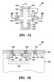
- FIG. 7A is a plan view of the measurement device of the present invention.
- FIG. 7B is a cross-sectional side view of the measurement device taken at line 7 B— 7 B of FIG. 7 A.
- FIG. 8A is a plan view of the reference device of the present invention.
- FIG. 8B is a cross-sectional side view of the reference device taken at line 8 B— 8 B of FIG. 8 A.
- FIG. 9 depicts a monitor set comprised of four pairs of measurement and reference devices of the present invention.
- FIG. 10 is a graph of data resulting from probing of the monitor set of the present invention.
- FIG. 11 is a plan view of a self-contained monitor device according to the present invention.
- FIGS. 12A through 12E show cross-sectional views illustrating the fabrication of a diode measurement and reference device pair according to the present invention.
- FIGS. 13A through 13C show a plan views of a wafer and the spatial dependence of stress monitoring devices.
- the invention utilizes a semiconductor structure upon which is located a diode which is surrounded by an isolation trench.
- the process of forming an isolation trench is well-known in the art.
- the isolation trench is filled with dielectric, typically an oxide or nitride.
- the resulting structure can be employed as a device for monitoring mechanical stress acting upon the semiconductor structure at the location of the diode.
- the trench isolation causes the semiconductor structure to behave much the same as a piezoresistive device, in that the effects of induced mechanical stress can modulate the nominal electrical behavior of a properly designed device, or array of such devices, for the purpose of measuring the induced stress. Extrinsically generated stress will also modulate device behavior and this stress, too, can effectively be measured.
- the end result is a stress monitor that measures stresses on a microscopic level, rather than only at the coarser device level.
- the surface tensile stress is primarily caused by the combination of the trench fill and the surface passivation films, such as silicon oxides and nitrides, which can cause dislocations and gate oxide defects.
- Surface tensile stress can retard or enhance oxide growth, which can in turn increase “bird's-beaking” in some manufacturing processes.
- bird's beak refers to a structural feature produced as a result of the lifting of the edges of the nitride layer during subsequent oxidation steps. Compressive trench stress can result in corner device turn-on, and anomalous PFET behavior.
- deep trench capacitors which share similar fabrication processes to trench isolation, also have similar stress-related problems, namely those due to shear stress causing dislocations, and compressive stress causing spurious electron-hole pair generation.
- Observed stress-induced device parametric changes include bandgap effects of carrier density, which varies exponentially, and changes in mobility, which varies linearly; saturation current (“I d ”) which can be enhanced or retarded up to about 7%; and reduced boron out-diffusion in positive-channel field effect transistor (“PFET”) source/drains (“S/D”), which directly affects the electrical channel length, L eff .
- I d saturation current
- S/D positive-channel field effect transistor
- FIG. 1 is a perspective view of a wafer portion 100 , containing a typical field effect transistor (“FET”) device, showing the channel 110 of channel length (“L”) 120 and the channel width (“W”) 130 .
- FET field effect transistor
- Trench isolation 140 is shown along the length of the device 110 .
- Trench isolation 140 exists (but is not shown) at the extrema along the width of the device 110 as well, where it forms the outer border of the S/D diffusions 150 .
- Two perspectives are indicated, A and B.
- FIG. 2 is a cross-sectional view of the typical FET device 110 , viewed at perspective B in FIG. 1, as constructed in a substrate 230 and capped with a polysilicon layer 240 , through the gate/channel region 210 parallel to the channel width 130 .
- the symbol “ ⁇ ” 220 is used to indicate stress.
- stress affects mobility (“ ⁇ ”), the effective electrical channel length (“L eff ”), and the drain-to-source current at maximum drain bias (“I dsat ”)
- stress affects the threshold voltage (“V t ”), the effective electrical channel width (“W eff ”), the mobility (“ ⁇ ”), and to second order, L eff
- V t threshold voltage
- W eff effective electrical channel width
- ⁇ mobility
- L eff second order, L eff
- the stress affects V t and I dsat , and to some extent, ⁇ .
- W decreases, ⁇ increases in magnitude.
- the strong modulation of the minority carrier density by stress can be advantageously used to monitor process-induced stress due to reductions in channel width W.
- FIG. 3 is a cross-sectional view along perspective A in FIG. 1 of a portion of a semiconductor substrate 300 containing a typical device 310 , through the channel region (in the channel length direction), showing where L eff is measured. Note that this measurement excludes the S/D extension regions 320 , and the S/D diffusion regions 330 .
- FIG. 4 is a graph representing the deviation of actual, measured, effective electrical channel length (L eff ) for an FET versus the design channel length (L design )
- the graph presents data for three devices, namely, an ideal device, an NFET device, and a PFET device.
- the ideal relationship is equality, which is the straight-line relationship in the graph.
- the effective channel length, L eff is less than the design length, L design , and therefore its trend generally lies below the ideal curve, except as shown at very small channel lengths, where the PFET trends above the ideal, the NFET farther below.
- FIG. 5 is a graph representing the dependence of FET effective, electrical channel length, L eff , on the device width, W d , for the ideal device, an NFET device, and a PFET device.
- W d moving to the right along the horizontal axis
- the design and electrical channel lengths are nearly equal. This is represented by the horizontal line labeled “Ideal”.
- Ideal the horizontal line labeled “Ideal”.
- the present invention takes advantage of the strong dependence of the minority carrier density on mechanical stress in order to measure its effects on the electrical devices described above.
- the method of the present invention describes both a diode structure and a non-diode, reference structure.
- the reference structure is necessary to reduce or entirely factor out the effects of parasitic devices in the diode structure itself.
- Diode current is measured in either forward or reverse bias volts (“V”). Only the forward bias case is discussed herein.
- I d (V, ⁇ ,W) The relationship of measured net diode current, I d (V, ⁇ ,W) due to stress induced by two isolation trenches spaced a distance (“W”) apart is expressed by equation (1):
- I r is the reference device current
- ⁇ is hydrostatic stress
- ⁇ is the stress activation volume of silicon (i.e., on the order of 10 ⁇ 22 cm 3 )
- k is Boltzmann's constant (1.38 ⁇ 10 ⁇ 23 J/K (joules/kelvin))
- T is the temperature (°K).
- Both the diode and reference devices embodied by this invention require an N well diffusion which forms a junction with a p+ diffusion. This junction forms a parasitic diode, the characteristics of which need to be accounted for in extracting the dependence of diode current on mechanical stress.
- V well is the p+ to N well bias.
- the reference device is described in detail infra.
- the exponential dependence of I d with stress is due to the change in bandgap induced by stress, thus strongly modulating the local minority carrier density.
- I 0 is the standard pre-factor which depends upon carrier diffusion length. It is a weak, linear function of mechanical stress and can be approximated by its zero stress value.
- the reference device current, I r (V well , ⁇ ,W), has a voltage and stress dependence similar to that of I d , as shown by equation (3):
- I r ( V well , ⁇ ,W ) I 0 ⁇ ( e qV well /kT ⁇ 1) ⁇ e qV well /kT (3)
- V well The N well voltage (“V well ”) can be tuned independently of V for optimal sensitivity. However, in principle, for zeroing out the effects of the parasitic diode, V well should be set equal to the bias voltage V.
- FIG. 6A shows the dependence of the lateral n+/p+ diode current as a function of forward diode bias voltage, V f , at different stress states. The stress values used are typical of that exerted by the isolation region on a device due to the fabrication process. The current values are normalized to the value at 1.0 V. The stress is given in dynes/cm 2 .
- the values of stress shown, +/ ⁇ 4.0 ⁇ 10 9 dynes/cm 2 are near the allowable limit, i.e., near the critical shear stress, 1.0 ⁇ 10 10 dynes/cm 2 , of the silicon substrate, at which stress value a dislocation will occur.
- a positive stress value e.g., +4.0 ⁇ 10 9 dynes/cm 2
- a negative stress value e.g., ⁇ 4.0 ⁇ 10 9 dynes/cm 2
- FIG. 6B is a calculation of the diode stress as a function of the isolation trench spacing, W, which shows that stress can substantially modulate the magnitude of the diode current.
- FIG. 6C is a plot of the diode current difference relative to the reference device as a function of inverse trench spacing (1/W).
- the signal grows as the trench spacing shrinks, making the disclosed measurement device a sensitive detector of mechanical stress.
- the acquired signal can therefore be used to set a limit to the maximum allowable induced stress by calibration to previously determined L eff values for specific NFET/PFET characterizations.
- the mechanical stress data can be used to discriminate the effects of stress on device behavior from other process-induced variations, such as PC linewidth variations, spacer oxide thickness variations, and extension dopant implant variations.
- FIG. 7A is a plan view of the measurement device 700 of the present invention. (The fabrication process by which the measurement device 700 is formed is described infra in the discussion of FIGS. 12A through 12E.)
- FIG. 7B is a cross-sectional side view of the measurement device 700 taken at line 7 B— 7 B of FIG. 7 A. It shows that the measurement device 700 comprises both p-type 710 and n-type 720 diffusions (thus forming a pn diode 730 ).
- the pn diode 730 is surrounded by trench isolation 740 in an n-well 750 , and this n-well 750 is in turn located in a p-well 760 .
- the measurement device 700 is substantially cross-shaped, that is, having pairs of arms extending at right angles from each other, for two reasons.
- the “horizontal” arms 744 having length L and width W, provide locations for the contacts spaced away from the n-well junction 735 .
- the “vertical” arms 764 provide for increased n-well junction 735 length which amplifies the desired effect and minimizes processes variations.
- the entire surface of the substrate, excluding electrical contact areas, is covered by a layer of dielectric material 725 .
- a layer of silicide 705 underlies the electrical contact 715 , 780 areas.
- FIG. 8A is a plan view of the reference device 800 of the present invention.
- FIG. 8B is a cross-sectional side view of the reference device 800 taken at line 8 B— 8 B of FIG. 8 A.
- the reference device 800 comprises a p-type diffusion 810 surrounded by trench isolation 840 in an n-well 850 , which in turn is located in a p-well 860 .
- An n-type diffusion 837 also permits electrical contact access to n-well 850 .
- Electrical contacts 880 to the p-diffusion 810 , and a contact 815 to the p-well, are provided.
- a parasitic vertical diode 890 is located at the p-type diffusion 810 and the n-well junction 835 .
- the horizontal arms 844 and the vertical arms 864 of the reference device 800 are essentially identical in length and width to those of the measurement device 700 (FIGS. 7A, 7 B).
- the entire surface of the substrate, excluding electrical contact areas, is covered by a layer of dielectric material 825 .
- a layer of silicide 805 underlies the electrical contact 815 , 880 areas.
- FIG. 9 depicts a stress monitor set 900 comprised of pairs (A, B, C, D) of measurement devices 910 and reference devices 920 . These device pairs 910 , 920 differ only in the changes in their width (“W”) from one pair to another; all pairs 910 , 920 have the same length (“L”). The differences in device width (“W”) are useful to modulate the stress.
- FIG. 10 is a graph of typical data taken from the monitor set 900 via application of test probes at: n-well contacts 912 for the measurement devices 910 ; 922 for the reference devices 920 ; p-well contacts 914 for the measurement devices 910 ; and 924 for the reference devices 920 .
- the monitor set 900 could be probed repeatedly throughout wafer fabrication, from contact formation through completion of the wafer by bringing the contacts up through all the wiring levels.
- I m is the current measured in the diode structure and I r is the current in the reference device.
- the current differential (I m ⁇ I r ) vs. 1/W is plotted, and can be compared to FIG. 6 C.
- I m is the current measured in the diode structure
- I r is the current in the reference device.
- the current differential (I m ⁇ I r ) vs. 1/W is plotted, and can be compared to FIG. 6 C.
- FIG. 10 is a graph
- V initial the first measurement curve labeled V initial is obtained early in wafer fabrication.
- V stress is measured later in the wafer fabrication process. If the stress has increased, the V stress measurement will have a greater current differential (I m ⁇ I r ) than the initial measurement. The difference between V initial and V stress indicates size sensitivity to stress.
- FIG. 11 is a plan view of a self-contained monitor device 1100 according to the present invention.
- the monitor set 1100 is comprised of pairs of measurement devices 1150 and reference devices 1160 . These device pairs 1150 , 1160 are surrounded by trench isolation 1110 , and are formed in an n-well 1120 .
- the n-well 1120 is itself bounded by a second trench isolation 1130 , and formed in a p-well 1140 .
- Table 1, infra indicates voltage levels for various contacts (e.g., I, II, III, IV, V) as indicated in FIG. 11 .
- FIGS. 12A through 12E show cross-sectional views illustrating the fabrication of a diode measurement device 1280 and reference device 1290 pair according to the present invention.
- a silicon substrate 1200 has been provided with a p-well 1210 into which dielectric trench isolation 1220 has been formed using techniques known in the art.
- n-wells 1230 have been formed.
- the measurement p-diffusion 1240 , reference p-diffusion 1250 , and the p-well contact diffusion 1250 have been formed by an ion implantation of boron at 10 Kev and at a dose of 10 15 atoms/cm 2 .
- FIG. 12A a silicon substrate 1200 has been provided with a p-well 1210 into which dielectric trench isolation 1220 has been formed using techniques known in the art.
- n-wells 1230 have been formed.
- the measurement p-diffusion 1240 , reference p-diffusion 1250 , and the p-well contact diffusion 1250 have been formed
- the diode n-diffusion 1245 and reference n-well contact 1265 have been formed by an ion implantation of arsenic at 25 Kev and at a dose of 10 15 atoms/cm 2 .
- the diode measurement device 1280 and reference device 1290 pair has been completed through the contact level with stud contacts 1270 , silicide layer 1275 , and insulative dielectric layer 1295 .
- semi-recessed oxide (“SROX”) can be used in place of trench isolation. The process for forming SROX is well known in the art.
- a silicon wafer 1310 is shown.
- the wafer diameter can be of a typical industry standard, either about 8 inches or 12 inches.
- the surface of the wafer 1310 defines the (1 0 0) crystal plane or crystal direction. In this example, the (1 0 0) crystal direction is along an axis (not shown) perpendicular to the page.
- a single notch 1320 is located at the perimeter of the wafer 1310 , and is present for manufacturing purposes. This notch 1320 is located on a single radius 1360 from the center point 1330 of the wafer 1310 .
- Crystal directions are defined with respect to the notch 1320 . These crystal directions are (1 1 0) and ( ⁇ overscore (1) ⁇ 1 0).
- the (1 1 0) crystal direction is defined by the radius 1360 extending from the wafer's center point 1330 to the notch 1320 .
- the ( ⁇ overscore (1) ⁇ 1 0) crystal direction is defined by a radius 1380 extending from center point 1330 in a direction rotated 90 degrees from crystal direction (1 1 0) and radius 1360 .
- radius 1370 extending from center point 1330 in a direction rotated 45 degrees from crystal direction (1 1 0) and radius 1360 , defines crystal direction (0 1 0).
- the current conduction properties are equivalent along the (1 1 0) and ( ⁇ overscore (1) ⁇ 1 0) directions (i.e., radii 1360 and 1380 , respectively).
- the current conduction properties in the plane of the wafer differ along the (0 1 0) direction from those along the (1 0 0) direction (i.e., perpendicular to the paper).
- the stress couples with the electric field and current perpendicular to the wafer surface, i.e., along the (1 0 0) direction, differently from any in-plane direction.
- Equation 1 the ( ⁇ ) product (see Equation 1) has a different magnitude for the same physical fabrication process, for the (1 0 0) and (0 1 0) crystal directions in the exponential stress term in previously defined Equation 1, supra, which defines the stress modulated current flow.
- stress monitoring structures 1390 such as embodied in FIG. 11, so that the diode current flow is along the different crystal directions in a coplanar arrangement.
- This arrangement is highly advantageous for detecting the differences in current conduction due to stress for devices similarly rotated.
- the stress magnitude has a radial dependence, from center-to-edge of the wafer 1310 .
- the 13B shows a pair of stress monitoring structures 1390 , 1392 on a wafer 1330 .
- One stress monitoring structure 1390 is oriented along the (1 1 0) crystal direction.
- the second stress monitoring structure 1392 is oriented along the (0 1 0) crystal direction.
- the diode current minus the reference current, (I m ⁇ I r ) is generally different for any crystal direction for any stress state.
- strategically placing and aligning stress detection structures 1390 , 1392 as shown in FIG. 13C allows sampling of a more complete spatial dependence of stress and diode current conduction on the wafer 1310 .
- the stresses exhibit an orientational or rotational dependence with respect to the semiconductor wafer. This information must be considered when placing the measurement and reference devices in the semiconductor wafer under test.
- these stress sensors can be embedded on product chips or monitor wafers. If on-chip, then maps of chip-level stress dependence can be determined, which should be related to wafer angular and radial stress dependence.
Abstract
A method is presented for measuring and monitoring the mechanical stress at the device level which occurs intrinsically during the fabrication process or which is induced via extrinsic means. The method applies the fact that the current-voltage (I-V) characteristics of a diode change as the diode is subjected to mechanical stress. The method is applicable to monitoring stress at the microscopic and device levels at various stages in the semiconductor wafer fabrication process. Apparatus for implementing the method is also presented.
Description
1. Technical Field
The present invention relates generally to the field of semiconductor device formation, and more specifically to a method and apparatus, integrated with said devices, for measuring mechanical stress induced in those devices. Such stress is either induced by the intrinsic fabrication process of the devices, or by extrinsic means, such as a vacuum chuck used during electrical tests. The method is particularly useful for measuring mechanical stress on semiconductor devices induced by the process of formation of either dielectric-filled isolation trenches or by semi-recessed oxide (SROX) isolation regions, which abut the devices of interest. The process of forming such isolation regions is well known in the art to be a significant source of stress.
2. Related Art
Dielectric-filled trench isolation is a common method of electrically isolating solid state silicon devices. It is especially common in complementary metal-oxide semiconductor (“CMOS”) technology as an alternative to back-biased isolation diffusion techniques used in negative-channel metal-oxide semiconductor (“NMOS”), positive-channel metal-oxide semiconductor (“PMOS”), or bipolar technologies. However, dielectric-filled trench isolation is difficult to implement in CMOS technology.
There are two significant drawbacks to the use of dielectric-filled trench isolation. First, the oxidation of the etched trench, which induces generally compressive stresses into the laterally adjacent silicon. Second, there is a densification of the dielectric that is deposited to fill the trench, and this densification induces tensile stress into the adjacent silicon. Thus, at the conclusion of the isolation trench construction process, the stress induced in the silicon is both compressive close to the surface, and tensile deeper down. These resulting stresses effect both device defects and device parameters.
Certain aspects of trench isolation as used in semiconductor structures causes the semiconductor structure to behave much the same as a piezoresistive device (i.e., a device whose resistance changes with the applied stress), and the effects of induced mechanical stress can modulate the nominal electrical behavior of a properly designed device, or array of such devices, for the purpose of measuring the induced stress. It is to be noted that extrinsically generated stress will also modulate device behavior and that this stress, too, can effectively be measured.
Devices known in the related art are designed to measure stress under controlled conditions, and are not meant to measure the process-induced stresses which are an accidental by-product of very large-scale integration (“VLSI”) fabrication.
Therefore, it would be most useful to be able to monitor stress during semiconductor device fabrication with the aim of modifying processes so as to reduce, or at least control, the stress and its resultant effects.
The invention disclosed herein presents a method and related structures that enable monitoring of stress acting upon a semiconductor structure. A method and apparatus for measuring the stress at microscopic levels is disclosed. The invention relies on the dimensional dependence between the width of a device and the inherent resistivity in the device.
The present invention discloses a method and apparatus used to measure the stress at a sub-chip (i.e., device and chip) level with resolution of stress effects on electrical conduction. The present invention permits obtaining data on the position dependence of stress effects on devices, including orientational effects on a semiconductor wafer or substrate used in production of VLSI devices and circuits. The present invention also allows monitoring of the dependence of stress on device size, particularly via wide-to-narrow diode behavior.
The present invention provides a structure for measuring stress in a semiconductor device comprising: a pn diode formed on the surface of a semiconductor device, said diode being bounded by a first shallow trench isolation region having predetermined dimensions; a diffusion region formed on the surface of the wafer, said diffusion region being bound by a second shallow trench isolation region having the same dimensions as the first shallow trench region; and contacts formed on said diode and diffusion region for passing current through the diode and through said diffusion region.
The present invention additionally provides a method of monitoring stress in a silicon substrate comprising the steps of: forming a first device comprising a pn diode in a first n-well region of a p-well formed in said silicon substrate, said pn diode having a geometry defined by a dielectric-filled trench; forming a second device comprising a p-type diffusion region in a second n-well region formed in said p-well region of said silicon substrate, said second n-well region having a geometry substantially the same as the geometry of said first n-well region and defined by a dielectric-filled trench; subtracting a first current measurement through said second device from a first current measurement from said first device.
The present invention further provides a method of using a stress monitor structure formed in a semiconductor wafer comprising the steps of: applying a current to the stress monitor structure; measuring a resultant bias voltage induced in the stress monitor structure by the current; comparing the stress-induced resultant bias voltage to a reference non-stress-induced bias voltage; and determining the amount of stress-induced electrical parameter variations in the semiconductor wafer.
The present invention also provides a stress monitoring unit comprising: a semiconductor material forming a base structure, said base structure containing a diode structure and a non-diode structure; said diode structure formed in the semiconductor material; said non-diode structure including a plurality of isolation trenches surrounding the diode structure, said isolation trenches being filled with a dielectric material; a system for applying an electrical potential across the diode structure, thereby inducing a diode current to flow through the diode structure; a system for measuring the diode current; and a system for translating the amount of diode current measured into dimensional units representing the stress on the base structure.
The present invention also discloses a stress monitoring set comprising: at least one pair of diode devices, or an array or plurality of diode devices, said pair consisting of a first device and a second device, wherein said first device is a reference device, and said second device (or array of secondary devices) is (are) a measurement device.
The present invention additionally discloses a stress monitoring system for monitoring mechanical stress in a semiconductor substrate containing trench isolation regions comprising: a semiconductor material forming a base structure, said base structure containing a diode structure and a non-diode structure; said diode structure formed in the semiconductor material; said non-diode structure including a plurality of isolation trenches surrounding the diode structure, said isolation trenches being filled with a dielectric material; a system for applying an electrical potential across the diode structure, thereby inducing a diode current to flow through the diode structure; a system for measuring the diode current; and a system for translating the amount of diode current measured into dimensional units representing the stress on the base structure.
For an understanding of the nature and advantages of the present invention, reference should be made to the following detailed description taken in connection with the accompanying drawings wherein:
FIG. 1 illustrates a typical FET in perspective showing channel length, L, and channel width, W.
FIG. 2 is a cross-section view of the typical FET of FIG. 1 through the gate/channel region parallel to the device width.
FIG. 3 is a cross-section view of the typical FET of FIG. 1 through the channel region, taken in the channel length direction.
FIG. 4 is a graph representing the deviation of actual, measured, effective electrical channel length for an FET versus the design channel length.
FIG. 5 is a graph representing the dependence of FET effective electrical channel length on the device width, Wd.
FIG. 6A is a graph showing the dependence of the lateral n+/p+ diode current as a function of forward diode bias voltage (“Vf”) at different stress states.
FIG. 6B is a graph showing the calculation of the diode stress as a function of isolation trench spacing (“W”).
FIG. 6C is a graph showing the diode current difference relative to reference as a function of inverse trench spacing (“1/W”) .
FIG. 7A is a plan view of the measurement device of the present invention.
FIG. 7B is a cross-sectional side view of the measurement device taken at line 7B—7B of FIG. 7A.
FIG. 8A is a plan view of the reference device of the present invention.
FIG. 8B is a cross-sectional side view of the reference device taken at line 8B—8B of FIG. 8A.
FIG. 9 depicts a monitor set comprised of four pairs of measurement and reference devices of the present invention.
FIG. 10 is a graph of data resulting from probing of the monitor set of the present invention.
FIG. 11 is a plan view of a self-contained monitor device according to the present invention.
FIGS. 12A through 12E show cross-sectional views illustrating the fabrication of a diode measurement and reference device pair according to the present invention.
FIGS. 13A through 13C show a plan views of a wafer and the spatial dependence of stress monitoring devices.
The invention utilizes a semiconductor structure upon which is located a diode which is surrounded by an isolation trench. The process of forming an isolation trench is well-known in the art. The isolation trench is filled with dielectric, typically an oxide or nitride. The resulting structure can be employed as a device for monitoring mechanical stress acting upon the semiconductor structure at the location of the diode. The trench isolation causes the semiconductor structure to behave much the same as a piezoresistive device, in that the effects of induced mechanical stress can modulate the nominal electrical behavior of a properly designed device, or array of such devices, for the purpose of measuring the induced stress. Extrinsically generated stress will also modulate device behavior and this stress, too, can effectively be measured. The end result is a stress monitor that measures stresses on a microscopic level, rather than only at the coarser device level.
There exist three types of stress which are of concern during semiconductor device fabrication. These are surface tensile stress, compressive trench stress, and shear stress.
The surface tensile stress is primarily caused by the combination of the trench fill and the surface passivation films, such as silicon oxides and nitrides, which can cause dislocations and gate oxide defects. Surface tensile stress can retard or enhance oxide growth, which can in turn increase “bird's-beaking” in some manufacturing processes.
The term “bird's beak” refers to a structural feature produced as a result of the lifting of the edges of the nitride layer during subsequent oxidation steps. Compressive trench stress can result in corner device turn-on, and anomalous PFET behavior.
In a related application, deep trench capacitors, which share similar fabrication processes to trench isolation, also have similar stress-related problems, namely those due to shear stress causing dislocations, and compressive stress causing spurious electron-hole pair generation.
Observed stress-induced device parametric changes include bandgap effects of carrier density, which varies exponentially, and changes in mobility, which varies linearly; saturation current (“Id”) which can be enhanced or retarded up to about 7%; and reduced boron out-diffusion in positive-channel field effect transistor (“PFET”) source/drains (“S/D”), which directly affects the electrical channel length, Leff.
Stress effects become very important as device dimensions shrink. FIG. 1 is a perspective view of a wafer portion 100, containing a typical field effect transistor (“FET”) device, showing the channel 110 of channel length (“L”) 120 and the channel width (“W”) 130. Trench isolation 140 is shown along the length of the device 110. Trench isolation 140 exists (but is not shown) at the extrema along the width of the device 110 as well, where it forms the outer border of the S/D diffusions 150. Two perspectives are indicated, A and B.
FIG. 2 is a cross-sectional view of the typical FET device 110, viewed at perspective B in FIG. 1, as constructed in a substrate 230 and capped with a polysilicon layer 240, through the gate/channel region 210 parallel to the channel width 130. The symbol “σ” 220 is used to indicate stress. In the channel length direction, stress affects mobility (“μ”), the effective electrical channel length (“Leff”), and the drain-to-source current at maximum drain bias (“Idsat”), In the device width direction (“W”), stress affects the threshold voltage (“Vt”), the effective electrical channel width (“Weff”), the mobility (“μ”), and to second order, Leff In the vertical direction (“V”), the stress affects Vt and Idsat, and to some extent, μ. Generally, as W decreases, σ increases in magnitude. In the present case, the strong modulation of the minority carrier density by stress can be advantageously used to monitor process-induced stress due to reductions in channel width W.
FIG. 3 is a cross-sectional view along perspective A in FIG. 1 of a portion of a semiconductor substrate 300 containing a typical device 310, through the channel region (in the channel length direction), showing where Leff is measured. Note that this measurement excludes the S/D extension regions 320, and the S/D diffusion regions 330.
FIG. 4 is a graph representing the deviation of actual, measured, effective electrical channel length (Leff) for an FET versus the design channel length (Ldesign) The graph presents data for three devices, namely, an ideal device, an NFET device, and a PFET device. The ideal relationship is equality, which is the straight-line relationship in the graph. Note that there is a significant departure from the ideal curve as Leff becomes smaller. Generally, the effective channel length, Leff, is less than the design length, Ldesign, and therefore its trend generally lies below the ideal curve, except as shown at very small channel lengths, where the PFET trends above the ideal, the NFET farther below. These excessive, small channel length deviations are due to a variety of physical effects, one of which is mechanical stress.
FIG. 5 is a graph representing the dependence of FET effective, electrical channel length, Leff, on the device width, Wd, for the ideal device, an NFET device, and a PFET device. For large Wd (moving to the right along the horizontal axis) the design and electrical channel lengths are nearly equal. This is represented by the horizontal line labeled “Ideal”. As Wd is reduced the effective channel length for both NFET and PFET can be drastically affected by the increasing mechanical stress due to the closer proximity of the isolation regions, and eventually exceed design specifications as shown.
For very small devices (e.g. , where Ldesign<0.2 μm) Leff rolls-off as a function of W for the NFET, but rolls-up for the PFET. This poses a problem, since the cross-hatched area 510 of FIG. 5 represents the region wherein the maximum performance of the device should be obtained. Significant contributors to the Leff roll-off/roll-up phenomena include both stress modulating the bandgap, and/or stress modulating the dopant lateral diffusion as discussed by T. Hook, et al. The following references are hereby incorporated by reference: T. B. Hook, S. Biesemanns, and J. Slinkman, “The dependence of channel length on channel width in narrow-channel CMOS Devices for 0.350-0.13 μm technologies.”, IEEE Elect. Dev. Lett., Feb. 21, 2000, pp85-87; and H. Park, “Point-defect based modeling of dislocation loops and stress effects on dopant diffusion in silicon,” PhD Thesis, Univ. Of Florida, 1993.
The present invention takes advantage of the strong dependence of the minority carrier density on mechanical stress in order to measure its effects on the electrical devices described above. The method of the present invention describes both a diode structure and a non-diode, reference structure. The reference structure is necessary to reduce or entirely factor out the effects of parasitic devices in the diode structure itself. First, a theory of operation of a diode structure under varying states of stress is described, then the embodiment of the diode and reference structures are described in detail.
Diode current is measured in either forward or reverse bias volts (“V”). Only the forward bias case is discussed herein. The relationship of measured net diode current, Id(V,σ,W) due to stress induced by two isolation trenches spaced a distance (“W”) apart is expressed by equation (1):
where the mechanically unstressed diode current is
I d(V,σ=0, W)=I 0·(e qV/kT−1) (2)
and where Ir is the reference device current, σ is hydrostatic stress, δΩ is the stress activation volume of silicon (i.e., on the order of 10−22 cm3), k is Boltzmann's constant (1.38×10⁻²³ J/K (joules/kelvin)), and T is the temperature (°K).
Both the diode and reference devices embodied by this invention require an Nwell diffusion which forms a junction with a p+ diffusion. This junction forms a parasitic diode, the characteristics of which need to be accounted for in extracting the dependence of diode current on mechanical stress.
For the reference device, Vwell is the p+ to Nwell bias. The reference device is described in detail infra. The exponential dependence of Id with stress is due to the change in bandgap induced by stress, thus strongly modulating the local minority carrier density. I0 is the standard pre-factor which depends upon carrier diffusion length. It is a weak, linear function of mechanical stress and can be approximated by its zero stress value. The reference device current, Ir(Vwell,σ,W), has a voltage and stress dependence similar to that of Id, as shown by equation (3):
The Nwell voltage (“Vwell”) can be tuned independently of V for optimal sensitivity. However, in principle, for zeroing out the effects of the parasitic diode, Vwell should be set equal to the bias voltage V. FIG. 6A shows the dependence of the lateral n+/p+ diode current as a function of forward diode bias voltage, Vf, at different stress states. The stress values used are typical of that exerted by the isolation region on a device due to the fabrication process. The current values are normalized to the value at 1.0 V. The stress is given in dynes/cm2. The values of stress shown, +/−4.0×109 dynes/cm2, are near the allowable limit, i.e., near the critical shear stress, 1.0×10¹⁰ dynes/cm2, of the silicon substrate, at which stress value a dislocation will occur. A positive stress value (e.g., +4.0×10⁹ dynes/cm2) indicates tensile stress, while a negative stress value (e.g., −4.0×10⁹ dynes/cm2) indicates compressive stress.
FIG. 6B is a calculation of the diode stress as a function of the isolation trench spacing, W, which shows that stress can substantially modulate the magnitude of the diode current.
Finally, FIG. 6C is a plot of the diode current difference relative to the reference device as a function of inverse trench spacing (1/W). Clearly, the signal grows as the trench spacing shrinks, making the disclosed measurement device a sensitive detector of mechanical stress. The acquired signal, for example, can therefore be used to set a limit to the maximum allowable induced stress by calibration to previously determined Leff values for specific NFET/PFET characterizations.
By correlation to In-Line-Test Leff data, the mechanical stress data can be used to discriminate the effects of stress on device behavior from other process-induced variations, such as PC linewidth variations, spacer oxide thickness variations, and extension dopant implant variations.
FIG. 7A is a plan view of the measurement device 700 of the present invention. (The fabrication process by which the measurement device 700 is formed is described infra in the discussion of FIGS. 12A through 12E.) FIG. 7B is a cross-sectional side view of the measurement device 700 taken at line 7B—7B of FIG. 7A. It shows that the measurement device 700 comprises both p-type 710 and n-type 720 diffusions (thus forming a pn diode 730). The pn diode 730 is surrounded by trench isolation 740 in an n-well 750, and this n-well 750 is in turn located in a p-well 760. Electrical contacts 780 to the p-type and n- type diffusions 710, 720 and a p-well contact 715 are provided. A parasitic diode 790 is located at the p-type diffusion 710 and n-well junction 735. The measurement device 700 is substantially cross-shaped, that is, having pairs of arms extending at right angles from each other, for two reasons. The “horizontal” arms 744, having length L and width W, provide locations for the contacts spaced away from the n-well junction 735. The “vertical” arms 764 provide for increased n-well junction 735 length which amplifies the desired effect and minimizes processes variations. The entire surface of the substrate, excluding electrical contact areas, is covered by a layer of dielectric material 725. A layer of silicide 705 underlies the electrical contact 715, 780 areas.
FIG. 8A is a plan view of the reference device 800 of the present invention. FIG. 8B is a cross-sectional side view of the reference device 800 taken at line 8B—8B of FIG. 8A. It can be seen that the reference device 800 comprises a p-type diffusion 810 surrounded by trench isolation 840 in an n-well 850, which in turn is located in a p-well 860. An n-type diffusion 837 also permits electrical contact access to n-well 850. Electrical contacts 880 to the p-diffusion 810, and a contact 815 to the p-well, are provided. Thus, a parasitic vertical diode 890 is located at the p-type diffusion 810 and the n-well junction 835. The horizontal arms 844 and the vertical arms 864 of the reference device 800 are essentially identical in length and width to those of the measurement device 700 (FIGS. 7A, 7B). The entire surface of the substrate, excluding electrical contact areas, is covered by a layer of dielectric material 825. A layer of silicide 805 underlies the electrical contact 815, 880 areas.
FIG. 9 depicts a stress monitor set 900 comprised of pairs (A, B, C, D) of measurement devices 910 and reference devices 920. These device pairs 910, 920 differ only in the changes in their width (“W”) from one pair to another; all pairs 910, 920 have the same length (“L”). The differences in device width (“W”) are useful to modulate the stress.
FIG. 10 is a graph of typical data taken from the monitor set 900 via application of test probes at: n-well contacts 912 for the measurement devices 910; 922 for the reference devices 920; p-well contacts 914 for the measurement devices 910; and 924 for the reference devices 920. Note that the monitor set 900 could be probed repeatedly throughout wafer fabrication, from contact formation through completion of the wafer by bringing the contacts up through all the wiring levels. In FIG. 10, Im is the current measured in the diode structure and Ir is the current in the reference device. The current differential (Im−Ir) vs. 1/W is plotted, and can be compared to FIG. 6C. In FIG. 10, the first measurement curve labeled Vinitial is obtained early in wafer fabrication. A subsequent curve, Vstress, is measured later in the wafer fabrication process. If the stress has increased, the Vstress measurement will have a greater current differential (Im−Ir) than the initial measurement. The difference between Vinitial and Vstress indicates size sensitivity to stress.
FIG. 11 is a plan view of a self-contained monitor device 1100 according to the present invention. The monitor set 1100 is comprised of pairs of measurement devices 1150 and reference devices 1160. These device pairs 1150, 1160 are surrounded by trench isolation 1110, and are formed in an n-well 1120. The n-well 1120 is itself bounded by a second trench isolation 1130, and formed in a p-well 1140. Table 1, infra, indicates voltage levels for various contacts (e.g., I, II, III, IV, V) as indicated in FIG. 11.
| TABLE 1 | |
| Contact | Voltage Level |
| I | biased at 0 to +2 v |
| II | ground (0 V) |
| III | biased at 0 to +2 v |
| IV | ground (0 V) |
| V | ground (0 V)* |
| *Alternatively, a −1 V back bias can be applied to p-well contact V to minimize substrate leakage; this may be necessary to implement the invention in future devices. | |
FIGS. 12A through 12E show cross-sectional views illustrating the fabrication of a diode measurement device 1280 and reference device 1290 pair according to the present invention. In FIG. 12A a silicon substrate 1200 has been provided with a p-well 1210 into which dielectric trench isolation 1220 has been formed using techniques known in the art. In FIG. 12B, n-wells 1230 have been formed. In FIG. 12C, the measurement p-diffusion 1240, reference p-diffusion 1250, and the p-well contact diffusion 1250 have been formed by an ion implantation of boron at 10 Kev and at a dose of 1015 atoms/cm2. In FIG. 12D, the diode n-diffusion 1245 and reference n-well contact 1265 have been formed by an ion implantation of arsenic at 25 Kev and at a dose of 1015 atoms/cm2. In FIG. 12E, the diode measurement device 1280 and reference device 1290 pair has been completed through the contact level with stud contacts 1270, silicide layer 1275, and insulative dielectric layer 1295. Alternatively, semi-recessed oxide (“SROX”) can be used in place of trench isolation. The process for forming SROX is well known in the art.
Referring now to FIG. 13A, a silicon wafer 1310 is shown. The wafer diameter can be of a typical industry standard, either about 8 inches or 12 inches. The surface of the wafer 1310 defines the (1 0 0) crystal plane or crystal direction. In this example, the (1 0 0) crystal direction is along an axis (not shown) perpendicular to the page. A single notch 1320 is located at the perimeter of the wafer 1310, and is present for manufacturing purposes. This notch 1320 is located on a single radius 1360 from the center point 1330 of the wafer 1310.
Crystal directions are defined with respect to the notch 1320. These crystal directions are (1 1 0) and ({overscore (1)} 1 0). The (1 1 0) crystal direction is defined by the radius 1360 extending from the wafer's center point 1330 to the notch 1320. The ({overscore (1)} 1 0) crystal direction is defined by a radius 1380 extending from center point 1330 in a direction rotated 90 degrees from crystal direction (1 1 0) and radius 1360. Similarly, radius 1370, extending from center point 1330 in a direction rotated 45 degrees from crystal direction (1 1 0) and radius 1360, defines crystal direction (0 1 0).
The current conduction properties are equivalent along the (1 1 0) and ({overscore (1)} 1 0) directions (i.e., radii 1360 and 1380, respectively). However, as is well known from semiconductor solid state physics, the current conduction properties in the plane of the wafer differ along the (0 1 0) direction from those along the (1 0 0) direction (i.e., perpendicular to the paper). Furthermore, the stress couples with the electric field and current perpendicular to the wafer surface, i.e., along the (1 0 0) direction, differently from any in-plane direction. This means that the (σ·δΩ) product (see Equation 1) has a different magnitude for the same physical fabrication process, for the (1 0 0) and (0 1 0) crystal directions in the exponential stress term in previously defined Equation 1, supra, which defines the stress modulated current flow. Thus, it is beneficial to align stress monitoring structures 1390, such as embodied in FIG. 11, so that the diode current flow is along the different crystal directions in a coplanar arrangement. This arrangement is highly advantageous for detecting the differences in current conduction due to stress for devices similarly rotated. Furthermore, as is well known in the art of VLSI device manufacturing, the stress magnitude has a radial dependence, from center-to-edge of the wafer 1310. FIG. 13B shows a pair of stress monitoring structures 1390, 1392 on a wafer 1330. One stress monitoring structure 1390 is oriented along the (1 1 0) crystal direction. The second stress monitoring structure 1392 is oriented along the (0 1 0) crystal direction. The diode current minus the reference current, (Im−Ir) , as discussed supra in the context of FIG. 10, is generally different for any crystal direction for any stress state.
Referring now to FIG. 13C, strategically placing and aligning stress detection structures 1390, 1392 as shown in FIG. 13C, allows sampling of a more complete spatial dependence of stress and diode current conduction on the wafer 1310.
Thus, the stresses exhibit an orientational or rotational dependence with respect to the semiconductor wafer. This information must be considered when placing the measurement and reference devices in the semiconductor wafer under test.
Also, these stress sensors can be embedded on product chips or monitor wafers. If on-chip, then maps of chip-level stress dependence can be determined, which should be related to wafer angular and radial stress dependence.
While embodiments of the present invention have been described herein for purposes of illustration, many modifications and changes will become apparent to those skilled in the art. Accordingly, the appended claims are intended to encompass all such modifications and changes as fall within the true spirit and scope of this invention.
Claims (18)
1. A stress monitoring set comprising:
at least one pair of diode devices, said pair comprising a first device and a second device, wherein said first device is a reference device, and said second device is a measurement device wherein each measurement device includes:
a diode structure formed in a semiconductor material; and
a non-diode structure including a plurality of isolation trenches surrounding the diode structure.
2. The stress monitoring set of claim 1 , wherein each reference device includes:
a diode structure formed in a semiconductor material; and
a non-diode structure including a plurality of isolation trenches surrounding the diode structure.
3. The stress monitoring set of claim 1 , further comprising a source of electrical current wherein the current is applied to the pairs of diode devices.
4. The stress monitoring set of claim 3 , wherein the stress monitoring set further includes a system for translating the amount of stress monitored into standardized data.
5. The stress monitoring set of claim 4 , wherein the stress monitoring set is self-contained.
6. A structure for measuring stress in a semiconductor device comprising:
a pn diode formed on the surface of a semiconductor device, said diode being bounded by a first isolation region having predetermined dimensions;
a diffusion region formed on the surface of the device, said diffusion region being bounded by a second isolation region having the same dimensions as the first isolation region; and
contacts formed on said diode and diffusion region for passing current through the diode and through said diffusion region.
7. The structure for measuring stress in a semiconductor device of claim 6 , wherein the first isolation region and the second isolation region are filled with dielectric material.
8. The structure for measuring stress in a semiconductor device of claim 6 , wherein the first isolation region and the second isolation region are shallow trench isolation regions.
9. The structure for measuring stress in a semiconductor device of claim 6 , wherein the first isolation region and the second isolation region are semi-recessed oxide regions.
10. A stress monitoring unit comprising:
a semiconductor material forming a base structure, said base structure containing a diode structure and a non-diode structure;
said diode structure formed in the semiconductor material;
said non-diode structure including a plurality of isolation trenches surrounding the diode structure, said isolation trenches being filled with a dielectric material;
a system for applying an electrical potential across the diode structure, thereby inducing a diode current to flow through the diode structure;
a system for measuring the diode current; and
a system for translating the amount of diode current measured into dimensional units representing the stress on the base structure.
11. The stress monitoring unit of claim 10 , wherein the dielectric material is an oxide.
12. The stress monitoring unit of claim 10 , wherein the diode structure further comprises a measurement device and a reference device.
13. The stress monitoring unit of claim 12 , wherein said measurement device further comprises:
p-type and n-type diffusions, each of which is surrounded trench isolation in an n-well;
a p-well surrounding said n-well;
contacts to the p-type and n-type diffusions, and to the p-well; and
a parasitic diode located at the junction of the p-type diffusion and the n-well junction.
14. The stress monitoring device of claim 12 , wherein the measurement device is formed substantially cross-shaped.
15. The stress monitoring unit of claim 12 , wherein said reference device further comprises:
a p-type diffusion surrounded by a trench isolation in an n-well;
a p-well surrounding said n-well;
contacts to the p-type diffusion, and to the p-well; and
a parasitic diode located at the junction of the p-type diffusion and the n-well junction.
16. The stress monitoring device of claim 15 , wherein the reference device is formed substantially cross-shaped.
17. The stress monitoring unit of claim 12 , wherein said cross-shaped portions, of said measurement device and said reference device, have substantially identical dimensions.
18. A stress monitoring system for monitoring mechanical stress in a semiconductor substrate containing trench isolation regions comprising:
a semiconductor material forming a base structure, said base structure containing a diode structure and a non-diode structure;
said diode structure formed in the semiconductor material;
said non-diode structure including a plurality of isolation trenches surrounding the diode structure, said isolation trenches being filled with a dielectric material;
a system for applying an electrical potential across the diode structure, thereby inducing a diode current to flow through the diode structure;
a system for measuring the diode current; and
a system for translating the amount of diode current measured into dimensional units representing the stress on the base structure.
Priority Applications (2)
| Application Number | Priority Date | Filing Date | Title |
|---|---|---|---|
| US09/695,038 US6441396B1 (en) | 2000-10-24 | 2000-10-24 | In-line electrical monitor for measuring mechanical stress at the device level on a semiconductor wafer |
| US10/194,642 US6649429B2 (en) | 2000-10-24 | 2002-07-11 | In-line electrical monitor for measuring mechanical stress at the device level on a semiconductor wafer |
Applications Claiming Priority (1)
| Application Number | Priority Date | Filing Date | Title |
|---|---|---|---|
| US09/695,038 US6441396B1 (en) | 2000-10-24 | 2000-10-24 | In-line electrical monitor for measuring mechanical stress at the device level on a semiconductor wafer |
Related Child Applications (1)
| Application Number | Title | Priority Date | Filing Date |
|---|---|---|---|
| US10/194,642 Division US6649429B2 (en) | 2000-10-24 | 2002-07-11 | In-line electrical monitor for measuring mechanical stress at the device level on a semiconductor wafer |
Publications (1)
| Publication Number | Publication Date |
|---|---|
| US6441396B1 true US6441396B1 (en) | 2002-08-27 |
Family
ID=24791295
Family Applications (2)
| Application Number | Title | Priority Date | Filing Date |
|---|---|---|---|
| US09/695,038 Expired - Fee Related US6441396B1 (en) | 2000-10-24 | 2000-10-24 | In-line electrical monitor for measuring mechanical stress at the device level on a semiconductor wafer |
| US10/194,642 Expired - Fee Related US6649429B2 (en) | 2000-10-24 | 2002-07-11 | In-line electrical monitor for measuring mechanical stress at the device level on a semiconductor wafer |
Family Applications After (1)
| Application Number | Title | Priority Date | Filing Date |
|---|---|---|---|
| US10/194,642 Expired - Fee Related US6649429B2 (en) | 2000-10-24 | 2002-07-11 | In-line electrical monitor for measuring mechanical stress at the device level on a semiconductor wafer |
Country Status (1)
| Country | Link |
|---|---|
| US (2) | US6441396B1 (en) |
Cited By (16)
| Publication number | Priority date | Publication date | Assignee | Title |
|---|---|---|---|---|
| US6624031B2 (en) * | 2001-11-20 | 2003-09-23 | International Business Machines Corporation | Test structure and methodology for semiconductor stress-induced defects and antifuse based on same test structure |
| US6759722B2 (en) * | 2000-03-31 | 2004-07-06 | Sharp Kabushiki Kaisha | Semiconductor device and method of manufacturing the same |
| US6808948B1 (en) * | 2002-12-11 | 2004-10-26 | Advanced Micro Devices, Inc. | Test structures to define COP electrical effects |
| US20050045879A1 (en) * | 2003-08-29 | 2005-03-03 | Udo Ausserlechner | Integrated circuitry and method for manufacturing the same |
| US20060151838A1 (en) * | 2005-01-12 | 2006-07-13 | International Business Machines Corporation | Enhanced pfet using shear stress |
| US20080173950A1 (en) * | 2007-01-18 | 2008-07-24 | International Business Machines Corporation | Structure and Method of Fabricating Electrical Structure Having Improved Charge Mobility |
| US20090098670A1 (en) * | 2007-10-15 | 2009-04-16 | Ji-Ho Hong | Semiconductor device for monitoring current characteristic and monitoring method for current characteristic of semiconductor device |
| US20090206316A1 (en) * | 2008-02-19 | 2009-08-20 | Qimonda Ag | Integrated circuit including u-shaped access device |
| US20120223309A1 (en) * | 2007-12-31 | 2012-09-06 | Advanced Micro Devices, Inc. | Test structure for monitoring process characteristics for forming embedded semiconductor alloys in drain/source regions |
| US20130175671A1 (en) * | 2010-09-30 | 2013-07-11 | Freescale Semiconductor, Inc. | Methods for processing a semiconductor wafer, a semiconductor wafer and a semiconductor device |
| US20140048897A1 (en) * | 2012-08-16 | 2014-02-20 | Omnivision Technologies, Inc. | Pixel with negatively-charged shallow trench isolation (sti) liner |
| CN103872021A (en) * | 2014-03-24 | 2014-06-18 | 上海华力微电子有限公司 | Semiconductor structure for WAT testing |
| US20150364402A1 (en) * | 2012-06-22 | 2015-12-17 | Infineon Technologies Ag | Monitor Structures and Methods of Formation Thereof |
| US9269607B2 (en) | 2014-06-17 | 2016-02-23 | Globalfoundries Inc. | Wafer stress control with backside patterning |
| US20160273991A1 (en) * | 2013-08-09 | 2016-09-22 | Infineon Technologies Ag | Circuits, methods, and computer programs to detect mechanical stress and to monitor a system |
| US10522380B2 (en) * | 2014-06-20 | 2019-12-31 | Applied Materials, Inc. | Method and apparatus for determining substrate placement in a process chamber |
Families Citing this family (12)
| Publication number | Priority date | Publication date | Assignee | Title |
|---|---|---|---|---|
| US6812717B2 (en) * | 2001-03-05 | 2004-11-02 | Boxer Cross, Inc | Use of a coefficient of a power curve to evaluate a semiconductor wafer |
| US6963393B2 (en) * | 2002-09-23 | 2005-11-08 | Applied Materials, Inc. | Measurement of lateral diffusion of diffused layers |
| US6878559B2 (en) * | 2002-09-23 | 2005-04-12 | Applied Materials, Inc. | Measurement of lateral diffusion of diffused layers |
| JP4408613B2 (en) * | 2002-09-25 | 2010-02-03 | Necエレクトロニクス株式会社 | Circuit simulation apparatus incorporating transistor diffusion layer length dependency and transistor model creation method |
| KR100563096B1 (en) * | 2003-08-22 | 2006-03-27 | 동부아남반도체 주식회사 | Detecting method for misalign of ion implanting |
| DE102004026145A1 (en) * | 2004-05-28 | 2006-05-11 | Advanced Micro Devices, Inc., Sunnyvale | Semiconductor structure with a voltage sensitive element and method for measuring an elastic stress in a semiconductor structure |
| JP2008501119A (en) * | 2004-05-28 | 2008-01-17 | アドバンスト・マイクロ・ディバイシズ・インコーポレイテッド | Semiconductor structure having stress sensitive elements and method for measuring stress in a semiconductor structure |
| DE102004036971B4 (en) * | 2004-07-30 | 2009-07-30 | Advanced Micro Devices, Inc., Sunnyvale | Technique for the evaluation of local electrical properties in semiconductor devices |
| KR20070043987A (en) * | 2004-07-30 | 2007-04-26 | 어드밴스드 마이크로 디바이시즈, 인코포레이티드 | Technique for evaluating local electrical characteristics in semiconductor devices |
| JP2006178907A (en) * | 2004-12-24 | 2006-07-06 | Matsushita Electric Ind Co Ltd | Circuit simulation method and device |
| US20080248598A1 (en) * | 2007-04-09 | 2008-10-09 | Rohit Pal | Method and apparatus for determining characteristics of a stressed material using scatterometry |
| FR2977368B1 (en) * | 2011-06-30 | 2014-01-31 | St Microelectronics Crolles 2 | METHOD FOR DETERMINING INDUCED LOCAL CONSTRAINTS IN A PLATE OF SEMICONDUCTOR MATERIAL BY CROSSING VIAS |
Citations (5)
| Publication number | Priority date | Publication date | Assignee | Title |
|---|---|---|---|---|
| US4125820A (en) | 1975-10-06 | 1978-11-14 | Honeywell Inc. | Stress sensor apparatus |
| US4144493A (en) * | 1976-06-30 | 1979-03-13 | International Business Machines Corporation | Integrated circuit test structure |
| US6265729B1 (en) * | 1997-10-14 | 2001-07-24 | American Microsystems, Inc. | Method for detecting and characterizing plasma-etch induced damage in an integrated circuit |
| US6291834B1 (en) * | 1999-03-15 | 2001-09-18 | Kabushiki Kaisha Toshiba | Semiconductor device and testing method therefor |
| US6339229B1 (en) * | 1999-10-21 | 2002-01-15 | Mitsubishi Denki Kabushiki Kaisha | Test structure for insulation-film evaluation |
Family Cites Families (5)
| Publication number | Priority date | Publication date | Assignee | Title |
|---|---|---|---|---|
| US5366906A (en) * | 1992-10-16 | 1994-11-22 | Martin Marietta Corporation | Wafer level integration and testing |
| JP3307240B2 (en) * | 1996-09-06 | 2002-07-24 | ヤマハ株式会社 | How to measure electronic shading damage |
| US6037792A (en) * | 1996-12-21 | 2000-03-14 | Stmicroelectronics, Inc. | Burn-in stress test mode |
| JP3251245B2 (en) * | 1998-06-10 | 2002-01-28 | 松下電器産業株式会社 | Method for evaluating semiconductor substrate and method for managing manufacturing process of semiconductor device |
| US6274397B1 (en) * | 1999-06-01 | 2001-08-14 | Taiwan Semiconductor Manufacturing Company Ltd. | Method to preserve the testing chip for package's quality |
-
2000
- 2000-10-24 US US09/695,038 patent/US6441396B1/en not_active Expired - Fee Related
-
2002
- 2002-07-11 US US10/194,642 patent/US6649429B2/en not_active Expired - Fee Related
Patent Citations (5)
| Publication number | Priority date | Publication date | Assignee | Title |
|---|---|---|---|---|
| US4125820A (en) | 1975-10-06 | 1978-11-14 | Honeywell Inc. | Stress sensor apparatus |
| US4144493A (en) * | 1976-06-30 | 1979-03-13 | International Business Machines Corporation | Integrated circuit test structure |
| US6265729B1 (en) * | 1997-10-14 | 2001-07-24 | American Microsystems, Inc. | Method for detecting and characterizing plasma-etch induced damage in an integrated circuit |
| US6291834B1 (en) * | 1999-03-15 | 2001-09-18 | Kabushiki Kaisha Toshiba | Semiconductor device and testing method therefor |
| US6339229B1 (en) * | 1999-10-21 | 2002-01-15 | Mitsubishi Denki Kabushiki Kaisha | Test structure for insulation-film evaluation |
Non-Patent Citations (1)
| Title |
|---|
| IBM Technical Disclosure Bulletin, vol. 34, No. 12, May 1992, On-Chip Electromigration Sensor Using Silicon Device, pp. 197-198. |
Cited By (34)
| Publication number | Priority date | Publication date | Assignee | Title |
|---|---|---|---|---|
| US6759722B2 (en) * | 2000-03-31 | 2004-07-06 | Sharp Kabushiki Kaisha | Semiconductor device and method of manufacturing the same |
| US6624031B2 (en) * | 2001-11-20 | 2003-09-23 | International Business Machines Corporation | Test structure and methodology for semiconductor stress-induced defects and antifuse based on same test structure |
| US7132325B2 (en) * | 2001-11-20 | 2006-11-07 | International Business Machines Corporation | Test structure and methodology for semiconductor stress-induced defects and antifuse based on same test structure |
| US6808948B1 (en) * | 2002-12-11 | 2004-10-26 | Advanced Micro Devices, Inc. | Test structures to define COP electrical effects |
| US7353712B2 (en) | 2003-08-29 | 2008-04-08 | Infineon Technologies Ag | Integrated circuitry and method for manufacturing the same |
| US20050045879A1 (en) * | 2003-08-29 | 2005-03-03 | Udo Ausserlechner | Integrated circuitry and method for manufacturing the same |
| DE10339939A1 (en) * | 2003-08-29 | 2005-04-14 | Infineon Technologies Ag | Integrated sounding arrangement and method for producing the same |
| DE10339939B4 (en) * | 2003-08-29 | 2010-02-11 | Infineon Technologies Ag | Integrated circuit arrangement and method for producing and evaluating the same |
| US20060286688A1 (en) * | 2003-08-29 | 2006-12-21 | Udo Ausserlechner | Integrated circuitry and method for manufacturing the same |
| US20070063309A1 (en) * | 2003-08-29 | 2007-03-22 | Udo Ausserlechner | Integrated circuitry and method for manufacturing the same |
| US7255010B2 (en) | 2003-08-29 | 2007-08-14 | Infineon Technologies Ag | Integrated circuitry and method for manufacturing the same |
| US7429498B2 (en) | 2003-08-29 | 2008-09-30 | Infineon Technologies Ag | Integrated circuitry and method for manufacturing the same |
| US20060151838A1 (en) * | 2005-01-12 | 2006-07-13 | International Business Machines Corporation | Enhanced pfet using shear stress |
| US7274084B2 (en) | 2005-01-12 | 2007-09-25 | International Business Machines Corporation | Enhanced PFET using shear stress |
| WO2006076535A1 (en) | 2005-01-12 | 2006-07-20 | International Business Machines Corporation | Enhanced pfet using shear stress |
| US20080173950A1 (en) * | 2007-01-18 | 2008-07-24 | International Business Machines Corporation | Structure and Method of Fabricating Electrical Structure Having Improved Charge Mobility |
| US20090098670A1 (en) * | 2007-10-15 | 2009-04-16 | Ji-Ho Hong | Semiconductor device for monitoring current characteristic and monitoring method for current characteristic of semiconductor device |
| KR100934791B1 (en) * | 2007-10-15 | 2009-12-31 | 주식회사 동부하이텍 | Semiconductor device for current characteristic measurement and current characteristic measurement method of semiconductor device |
| US20120223309A1 (en) * | 2007-12-31 | 2012-09-06 | Advanced Micro Devices, Inc. | Test structure for monitoring process characteristics for forming embedded semiconductor alloys in drain/source regions |
| US8530894B2 (en) * | 2007-12-31 | 2013-09-10 | Advanced Micro Devices, Inc. | Test structure for monitoring process characteristics for forming embedded semiconductor alloys in drain/source regions |
| US20090206316A1 (en) * | 2008-02-19 | 2009-08-20 | Qimonda Ag | Integrated circuit including u-shaped access device |
| US7994536B2 (en) * | 2008-02-19 | 2011-08-09 | Qimonda Ag | Integrated circuit including U-shaped access device |
| US20130175671A1 (en) * | 2010-09-30 | 2013-07-11 | Freescale Semiconductor, Inc. | Methods for processing a semiconductor wafer, a semiconductor wafer and a semiconductor device |
| US20170069554A1 (en) * | 2012-06-22 | 2017-03-09 | Infineon Technologies Ag | Monitor Structures and Methods of Formation Thereof |
| US20150364402A1 (en) * | 2012-06-22 | 2015-12-17 | Infineon Technologies Ag | Monitor Structures and Methods of Formation Thereof |
| US10014230B2 (en) * | 2012-06-22 | 2018-07-03 | Infineon Technologies Ag | Monitor structures and methods of formation thereof |
| US9530720B2 (en) * | 2012-06-22 | 2016-12-27 | Infineon Technologies Ag | Monitor structures and methods of formation thereof |
| US20140048897A1 (en) * | 2012-08-16 | 2014-02-20 | Omnivision Technologies, Inc. | Pixel with negatively-charged shallow trench isolation (sti) liner |
| US10352812B2 (en) * | 2013-08-09 | 2019-07-16 | Infineon Technologies Ag | Circuits, methods, and computer programs to detect mechanical stress and to monitor a system |
| US20160273991A1 (en) * | 2013-08-09 | 2016-09-22 | Infineon Technologies Ag | Circuits, methods, and computer programs to detect mechanical stress and to monitor a system |
| CN103872021A (en) * | 2014-03-24 | 2014-06-18 | 上海华力微电子有限公司 | Semiconductor structure for WAT testing |
| CN103872021B (en) * | 2014-03-24 | 2016-08-17 | 上海华力微电子有限公司 | Semiconductor structure for WAT test |
| US9269607B2 (en) | 2014-06-17 | 2016-02-23 | Globalfoundries Inc. | Wafer stress control with backside patterning |
| US10522380B2 (en) * | 2014-06-20 | 2019-12-31 | Applied Materials, Inc. | Method and apparatus for determining substrate placement in a process chamber |
Also Published As
| Publication number | Publication date |
|---|---|
| US20020190252A1 (en) | 2002-12-19 |
| US6649429B2 (en) | 2003-11-18 |
Similar Documents
| Publication | Publication Date | Title |
|---|---|---|
| US6441396B1 (en) | In-line electrical monitor for measuring mechanical stress at the device level on a semiconductor wafer | |
| US7132325B2 (en) | Test structure and methodology for semiconductor stress-induced defects and antifuse based on same test structure | |
| US8412487B2 (en) | Self heating monitor for SiGe and SOI CMOS devices | |
| US6521469B1 (en) | Line monitoring of negative bias temperature instabilities by hole injection methods | |
| US5519336A (en) | Method for electrically characterizing the insulator in SOI devices | |
| US7071044B1 (en) | Method of making a test structure for gate-body current and direct extraction of physical gate length using conventional CMOS | |
| US7989232B2 (en) | Method of using electrical test structure for semiconductor trench depth monitor | |
| US7132683B1 (en) | Dual purpose test structure for gate-body current measurement in PD/SOI and for direct extraction of physical gate length in scaled CMOS technologies | |
| CN101022105B (en) | Semiconductor device testing device and substrate for producing tester | |
| US20090098670A1 (en) | Semiconductor device for monitoring current characteristic and monitoring method for current characteristic of semiconductor device | |
| US6754553B2 (en) | Implant monitoring using multiple implanting and annealing steps | |
| Lee et al. | An anomalous device degradation of SOI narrow width devices caused by STI edge influence | |
| CN102142383B (en) | Method for detecting positions of wells | |
| US6265729B1 (en) | Method for detecting and characterizing plasma-etch induced damage in an integrated circuit | |
| US5841294A (en) | Method for measuring leakage current in junction region of semiconductor device | |
| US9383404B2 (en) | High resistivity substrate final resistance test structure | |
| US6362080B1 (en) | Formation of a vertical junction through process simulation based optimization of implant doses and energies | |
| CN108417536B (en) | Semiconductor structure and forming method and working method thereof | |
| US7838376B2 (en) | Non-destructive inline epi pattern shift monitor using selective epi | |
| US5831310A (en) | Semiconductor device for checking quality of a semiconductor region | |
| JP2964948B2 (en) | Semiconductor device and manufacturing method thereof. | |
| Terada et al. | A new VLSI memory cell using capacitance coupling | |
| Short et al. | Low dose ion implantation characterization for Vt control | |
| Draper et al. | Identification of Yield-Limiting Defects in a 0.5 Micron, Shallow Trench Isolation Technology | |
| Henderson et al. | Identification of Yield Limiting Defects in a 0.5 Micron, Shallow Trench Isolation Technology |
Legal Events
| Date | Code | Title | Description |
|---|---|---|---|
| FPAY | Fee payment |
Year of fee payment: 4 |
|
| REMI | Maintenance fee reminder mailed | ||
| LAPS | Lapse for failure to pay maintenance fees | ||
| STCH | Information on status: patent discontinuation |
Free format text: PATENT EXPIRED DUE TO NONPAYMENT OF MAINTENANCE FEES UNDER 37 CFR 1.362 |
|
| FP | Lapsed due to failure to pay maintenance fee |
Effective date: 20100827 |