US6399404B2 - Fabricating method of optical semiconductor device - Google Patents
Fabricating method of optical semiconductor device Download PDFInfo
- Publication number
- US6399404B2 US6399404B2 US09/407,091 US40709199A US6399404B2 US 6399404 B2 US6399404 B2 US 6399404B2 US 40709199 A US40709199 A US 40709199A US 6399404 B2 US6399404 B2 US 6399404B2
- Authority
- US
- United States
- Prior art keywords
- optical devices
- fabricating
- semiconductor substrate
- semiconductor
- optical
- Prior art date
- Legal status (The legal status is an assumption and is not a legal conclusion. Google has not performed a legal analysis and makes no representation as to the accuracy of the status listed.)
- Expired - Fee Related
Links
Images


Classifications
-
- H—ELECTRICITY
- H01—ELECTRIC ELEMENTS
- H01L—SEMICONDUCTOR DEVICES NOT COVERED BY CLASS H10
- H01L27/00—Devices consisting of a plurality of semiconductor or other solid-state components formed in or on a common substrate
- H01L27/15—Devices consisting of a plurality of semiconductor or other solid-state components formed in or on a common substrate including semiconductor components with at least one potential-jump barrier or surface barrier specially adapted for light emission
- H01L27/153—Devices consisting of a plurality of semiconductor or other solid-state components formed in or on a common substrate including semiconductor components with at least one potential-jump barrier or surface barrier specially adapted for light emission in a repetitive configuration, e.g. LED bars
- H01L27/156—Devices consisting of a plurality of semiconductor or other solid-state components formed in or on a common substrate including semiconductor components with at least one potential-jump barrier or surface barrier specially adapted for light emission in a repetitive configuration, e.g. LED bars two-dimensional arrays
-
- H—ELECTRICITY
- H01—ELECTRIC ELEMENTS
- H01S—DEVICES USING THE PROCESS OF LIGHT AMPLIFICATION BY STIMULATED EMISSION OF RADIATION [LASER] TO AMPLIFY OR GENERATE LIGHT; DEVICES USING STIMULATED EMISSION OF ELECTROMAGNETIC RADIATION IN WAVE RANGES OTHER THAN OPTICAL
- H01S5/00—Semiconductor lasers
- H01S5/02—Structural details or components not essential to laser action
- H01S5/0201—Separation of the wafer into individual elements, e.g. by dicing, cleaving, etching or directly during growth
-
- H—ELECTRICITY
- H01—ELECTRIC ELEMENTS
- H01S—DEVICES USING THE PROCESS OF LIGHT AMPLIFICATION BY STIMULATED EMISSION OF RADIATION [LASER] TO AMPLIFY OR GENERATE LIGHT; DEVICES USING STIMULATED EMISSION OF ELECTROMAGNETIC RADIATION IN WAVE RANGES OTHER THAN OPTICAL
- H01S5/00—Semiconductor lasers
- H01S5/06—Arrangements for controlling the laser output parameters, e.g. by operating on the active medium
- H01S5/062—Arrangements for controlling the laser output parameters, e.g. by operating on the active medium by varying the potential of the electrodes
- H01S5/0625—Arrangements for controlling the laser output parameters, e.g. by operating on the active medium by varying the potential of the electrodes in multi-section lasers
- H01S5/06255—Controlling the frequency of the radiation
- H01S5/06256—Controlling the frequency of the radiation with DBR-structure
-
- H—ELECTRICITY
- H01—ELECTRIC ELEMENTS
- H01S—DEVICES USING THE PROCESS OF LIGHT AMPLIFICATION BY STIMULATED EMISSION OF RADIATION [LASER] TO AMPLIFY OR GENERATE LIGHT; DEVICES USING STIMULATED EMISSION OF ELECTROMAGNETIC RADIATION IN WAVE RANGES OTHER THAN OPTICAL
- H01S5/00—Semiconductor lasers
- H01S5/10—Construction or shape of the optical resonator, e.g. extended or external cavity, coupled cavities, bent-guide, varying width, thickness or composition of the active region
- H01S5/12—Construction or shape of the optical resonator, e.g. extended or external cavity, coupled cavities, bent-guide, varying width, thickness or composition of the active region the resonator having a periodic structure, e.g. in distributed feedback [DFB] lasers
- H01S5/125—Distributed Bragg reflector [DBR] lasers
-
- H—ELECTRICITY
- H01—ELECTRIC ELEMENTS
- H01S—DEVICES USING THE PROCESS OF LIGHT AMPLIFICATION BY STIMULATED EMISSION OF RADIATION [LASER] TO AMPLIFY OR GENERATE LIGHT; DEVICES USING STIMULATED EMISSION OF ELECTROMAGNETIC RADIATION IN WAVE RANGES OTHER THAN OPTICAL
- H01S5/00—Semiconductor lasers
- H01S5/20—Structure or shape of the semiconductor body to guide the optical wave ; Confining structures perpendicular to the optical axis, e.g. index or gain guiding, stripe geometry, broad area lasers, gain tailoring, transverse or lateral reflectors, special cladding structures, MQW barrier reflection layers
- H01S5/2054—Methods of obtaining the confinement
- H01S5/2077—Methods of obtaining the confinement using lateral bandgap control during growth, e.g. selective growth, mask induced
Definitions
- the present invention relates to a fabrication method of an optical semiconductor device and, particularly, to a fabrication method of a semiconductor laser and an optical modulator for use in a WDM (wavelength division multiplexing) transmission system.
- WDM wavelength division multiplexing
- a semiconductor EA (electro-absorption) modulator or a LN (lithium niobate) modulator has been utilized.
- the EA modulator can be monolithically integrated with the DFB laser as the light source, it is effective in reducing the size and power consumption and is the key device of a high density WDM system. Since the basic purpose of the WDM system is to transmit optical signals having different wavelengths through a single optical fiber, DFB lasers having various oscillation wavelengths are required as light sources and optical modulators corresponding to the respective wavelengths are required.
- an element having only one oscillation wavelength or operation wavelength can be obtained from one semiconductor substrate.
- the gratings have the same pitch with respect to one direction of the substrate as shown in FIG. 18, that is, elements having different oscillation wavelengths are arranged according to some linear function, that is, linearly with respect to a certain direction of the substrate as shown in FIG. 19 ( a ). Therefore, when the elements are formed on a circular substrate, the number of elements formed in a center portion of the substrate becomes different from that of the elements formed in an edge portion thereof. Thus, the number of elements that can be fabricated on a single substrate varies substantially depending upon oscillation wavelength as shown in FIG. 19 ( b ). Therefore, the proposed technique is inadequate as the fabrication method of light source for WDM.
- An object of the present invention is to provide a fabrication method for fabricating optical semiconductor devices including DFB laser diodes having different oscillation wavelengths, EA modulators having different band gap wavelengths of absorption layers thereof or elements formed by the DFB laser diodes monolithically integrated with the EA modulators on a circular semiconductor substrate such as a 2-inch InP substrate, the number of semiconductor elements having a different one of operation wavelengths (oscillation wavelengths or absorption wavelengths), is constant.
- an object of the present invention is to provide a fabrication method with which a constant number of elements for each operation wavelength can be obtained most efficiently from a usual circular substrate.
- an optical semiconductor device fabrication method for simultaneously fabricating optical semiconductor devices having different operation wavelengths (operation energy) on a single circular semiconductor substrate is featured by that the number of elements having each of the operation wavelengths can be made constant.
- a first aspect of the present invention resides in a method for fabricating an optical semiconductor device on a circular semiconductor substrate, which is featured by comprising parabolically changing an operation band gap energy (band gap wavelength) of the optical semiconductor device from a center portion of the circular semiconductor substrate toward an outer periphery of the circular semiconductor substrate.
- a second aspect of the present invention resides in a method for fabricating a semiconductor laser on a circular semiconductor substrate, which is featured by comprising parabolically changing an oscillation wavelength of the semiconductor laser from a center portion of the circular semiconductor substrate toward an outer periphery of the circular semiconductor substrate.
- a third aspect of the present invention resides in the method for fabricating a semiconductor laser according to the second aspect, which is further featured by that the semiconductor laser is a DFB-LD (distributed feedback laser diode) or a DBR-LD (distributed Bragg reflector laser diode).
- the semiconductor laser is a DFB-LD (distributed feedback laser diode) or a DBR-LD (distributed Bragg reflector laser diode).
- a fourth aspect of the present invention resides in the method for fabricating a semiconductor laser according to the third aspect, which is further featured by that a pitch of gratings formed in a waveguide or in the vicinity of the waveguide is parabolically changed from a center portion of the circular semiconductor substrate toward an outer periphery of the circular semiconductor substrate.
- a fifth aspect of the present invention resides in the method for fabricating a semiconductor laser according to the third or fourth aspect, which is further featured by that Eb ⁇ Eg is constant in a range from ⁇ 5 meV to +15 meV and, preferably, from ⁇ 0 meV to +10 meV, where Eb is energy of Bragg wavelength (laser oscillation wavelength) determined by the gratings pitch and Eg is energy of a gain peak wavelength of an active layer of the laser.
- a sixth aspect of the present invention resides in a method for fabricating a semiconductor optical modulator of an EA type, on a circular semiconductor substrate, which is featured by comprising parabolically changing a band gap wavelength of an optical absorption layer of the semiconductor optical modulator from a center portion of the circular semiconductor substrate toward an outer periphery of the circular semiconductor substrate.
- a seventh aspect of the present invention resides in a method for fabricating a semiconductor optical integrated device having a DFB-LD monolithically integrated with a semiconductor optical modulator of an EA type or a DBR-LD monolithically integrated with a semiconductor optical modulator of an EA type, on a circular semiconductor substrate, which is featured by comprising parabolically changing both a band gap wavelength of an optical absorption layer of the semiconductor optical modulator and an oscillation wavelength of the DFB-LD or the DBR-LD from a center portion of the circular semiconductor substrate toward an outer periphery of the circular semiconductor substrate.
- An eighth aspect of the present invention resides in the method for fabricating a semiconductor laser according to the seventh aspect, which is further featured by that Em ⁇ Eb is constant in a range from 20 meV to 40 meV and, preferably, from 25 meV to 35 meV, where Em is band gap energy of the optical absorption layer of the EA modulator and Eb is energy of the DFB-LD or DBR-LD.
- a ninth aspect of the present invention resides in a method for fabricating an optical semiconductor device on a circular semiconductor substrate, which is featured by comprising growing a semiconductor layer constituting the optical semiconductor device by MOVPE (metal-organic vapor phase epitaxy) and changing a temperature of the semiconductor substrate such that the band gap wavelength of the epitaxially grown layer is parabolically changed in a surface of the semiconductor substrate from a center portion of the semiconductor substrate toward an outer periphery thereof.
- MOVPE metal-organic vapor phase epitaxy
- a tenth aspect to the present invention resides in a method for fabricating an optical semiconductor device on a circular semiconductor substrate, which is featured by comprising of growing a semiconductor layer constituting the optical semiconductor device by selective MOVPE using a dielectric film as a growth blocking mask and changing a width of the growth blocking mask such that the band gap wavelength of the epitaxially grown layer is parabolically changed in a surface of the semiconductor substrate from a center portion of the semiconductor substrate toward an outer periphery thereof.
- An eleventh aspect of the present invention resides in a method for fabricating an optical semiconductor device on a circular semiconductor substrate, which is featured by comprising of growing a semiconductor layer constituting said optical semiconductor device by selective MOVPE using a dielectric film as a growth blocking mask and changing a width of an opening portion of the growth blocking mask such that the band gap wavelength of the epitaxially grown layer is parabolically changed in a surface of said semiconductor substrate from a center portion of the semiconductor substrate toward an outer periphery thereof.
- a twelfth aspect of the present invention resides in the method of fabricating an optical semiconductor device according to any of the first to eleventh aspects, which is further featured by that the parabolic distribution of the operation and gap energy is approximated by a plurality of steps.
- a first effect of the present invention is that, in the fabrication method of an optical semiconductor device for forming elements having different operation wavelengths on a circular semiconductor substrate, the number of elements having each of operation wavelengths obtainable from the semiconductor substrate can be efficiently made constant.
- the reason for this is that the operation wavelengths of the optical semiconductor device are changed parabolically from a center portion of the substrate to an outer peripheral portion of the substrate.
- a second effect of the present invention is that an optical semiconductor device applied to a DFB laser can operate highly uniformly with low threshold current and high efficiency at any of different oscillation wavelengths thereof.
- the reason for this is that it is possible to always define an energy difference between DFB oscillation wavelength defined by the grating pitch and the gain peak wavelength defined by the crystal structure within a constant range.
- a third effect of the present invention is that an optical semiconductor device applied to an EA modulator integrated DFB laser can operate highly uniformly with low threshold current, high efficiency and high light extinction ratio, at any of different oscillation wavelengths thereof.
- the reason for this is that it is possible to always define an energy difference between DFB oscillation wavelength defined by the grating pitch and the gain peak wavelength defined by the crystal structure and an energy difference between the DFB oscillation wavelength and the band gap wavelength of the absorption layer of the modulator within a constant range.
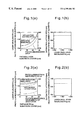
- FIGS. 1 ( a ) and 1 ( b ) show characteristics curves illustrating a principle of the present invention
- FIGS. 2 ( a ) and 2 ( b ) show characteristics curves illustrating the principle of the present invention
- FIG. 3 shows a characteristics curve illustrating the principle of the present invention
- FIG. 4 shows characteristics curves illustrating the principle of the present invention
- FIGS. 5 ( a ) and 5 ( b ) show characteristics curves illustrating the principle of the present invention
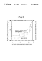
- FIG. 6 shows characteristics distributions illustrating the principle of the present invention
- FIG. 7 shows characteristics curves illustrating the principle of the present invention
- FIG. 8 shows characteristics curves illustrating the principle of the present invention
- FIG. 9 shows a circular semiconductor substrate formed with diffraction lattices thereon, illustrating an embodiment of the present invention
- FIG. 10 shows a mask pattern formed on the circular semiconductor substrate, illustrating the embodiment of the present invention.
- FIGS. 11 ( a ) to 11 ( e ) show cross sections of a wafer illustrating manufacturing steps according to the embodiment of the present invention
- FIG. 12 shows a mask pattern illustrating another embodiment of the present invention.
- FIGS. 13 ( a ) to 13 ( c ) show cross sections of a wafer illustrating manufacturing steps according to the embodiment shown in FIG. 12;
- FIG. 14 shows a circular semiconductor substrate formed with discrete partial gratings, illustrating another embodiment of the present invention.
- FIG. 15 shows a mask pattern formed on the circular semiconductor substrate shown in FIG. 14;
- FIG. 16 shows a portion of the mask pattern shown in FIG. 15;
- FIG. 17 shows a structure of an element illustrating another embodiment of the present invention.
- FIG. 18 shows a mask pattern used in a conventional fabrication method
- FIGS. 19 ( a ) and 19 ( b ) show characteristics curves of a conventional element.
- an operating band gap energy (band gap wavelength) of the optical semiconductor device is parabolically changed from a center portion of the circular semiconductor substrate toward an outer periphery thereof. That is, representing the distance from the center of the circular semiconductor substrate by R, the operating band gap energy at the center of the circular semiconductor substrate by E(0) and the operating band gap energy at a position which is distance R from the center of the circular semiconductor substrate by E(R),
- this structure By this structure, yield of elements for each of the different operating wavelengths is made constant and maximum.
- this structure is suitable for the usual MOVPE apparatus in which raw material gas is supplied from the top of the semiconductor substrate, because the distribution of the crystal growth layer in the semiconductor substrate surface becomes shaped like the concentric circle with the flow of raw material gas from center portion of the circular semiconductor substrate toward an outer periphery thereof.
- the pitch of grating which defines the oscillation wavelength of a DFB laser
- EB electron beam
- a photo-luminescence wavelength (band gap wavelength) distribution in forming an active layer of a DFB laser and/or an absorption layer of an optical modulator by using selective MOVPE it has been known that thickness and constituents of a selectively grown layer can be controlled by changing a width of a growth blocking mask and, therefore, it is possible to control the photo-luminescence wavelength distribution of the selectively grown layer by changing the width of the growth blocking mask from the center portion of the substrate toward the outer periphery thereof as shown in FIGS.
- the film thickness can be controlled by a width of an opening portion of the mask, it is possible to control the photo-luminescence wavelength distribution of the selectively grown layer by changing the width of the opening portion of the mask from the center portion of the substrate toward the outer periphery thereof as shown in FIG. 7 .
- an InGaAsP layer is grown by MOVPE, a ratio of arsenic to phosphor of the layer, which are group-V materials, is changed with crystal growing temperature.
- FIG. 3 shows a relation between the difference and the laser oscillation threshold current.
- abscissa indicates a value of the difference between ⁇ DFB and the gain peak wavelength, converted into energy. That is, representing the oscillation wavelength energy by E(DFB) and the gain peak energy by E(gain peak),
- ⁇ E2 should be within a range 20 ⁇ 40 meV and, preferably, 25 ⁇ 35 meV. Therefore, in the present invention, it is necessary to control the DFB laser oscillation wavelength distribution and the photo-luminescence wavelength distribution of the EA modulator in the surface of the substrate such that the above mentioned conditions are satisfied.
- gratings 100 each 10 ⁇ m wide were formed on a 2-inch (100) n-InP substrate 101 with an interval of 300 ⁇ m between adjacent grating, as shown in FIG. 9, by using EB exposure and chemical etching.
- the pitch of the grating 100 was changed parabolically from 240.4 nm in the center portion of the substrate to 243.3 nm in the outer periphery as shown in FIG. 1 ( a ). That is, representing the distance from the center of the circular semiconductor substrate by R [mm], the pitch of the gratings 100 at the center of the circular semiconductor substrate by P(0) and the pitch of the gratings 100 at the position which is distant R from the center of the circular semiconductor substrate by P(R),
- a SiO 2 film 102 having thickness of 100 nm was deposited thereon by atmospheric pressure thermal CVD (chemical vapor deposition). Thereafter, a pair of patterns each Wm wide were formed on each grating 100 in [011] direction with a gap being 1.5 ⁇ m therebetween as a selective growth mask by partially removing the SiO 2 film 102 with using photolithography and chemical etching, as shown in FIG. 10 .
- the width Wm of the mask was changed parabolically from 16 ⁇ m in the center portion of the substrate to 18.5 ⁇ m in the outer periphery thereof as shown in FIG. 5 ( a ).
- an InGaAsP strain MQW (multiple quantum well) structure was selectively grown by low pressure MOVPE at growing temperature of 625° C. and growing pressure of 100 hPa, as shown by a cross sectional structure in FIG. 11 ( a ).
- ⁇ g band gap wavelength
- the wavelength was 1.538 ⁇ m in the center portion of the substrate, was increased parabolically toward the outer periphery thereof and was 1.565 ⁇ m at the outermost portion of the outer periphery, remote from the center portion by 25 mm, as shown in FIG. 11 ( a ).
- a SiO 2 mask 104 was formed on only an upper surface of the strain MQW structure as shown in FIG. 11 ( b ) and current block layers 105 , 106 and 107 were formed by using the SiO 2 mask 104 as a selective growing mask, to bury the strain MQW structure, as shown in FIG.
- the DFB laser oscillation wavelength in the center portion of the substrate is 1.543 ⁇ m, is increased parabolically toward the outer periphery and is 1.560 ⁇ m at the outermost portion of the outer periphery, remote from the center of the substrate by 25 mm, as shown in FIG. 1 ( a ). Further, the number of elements for each oscillation wavelength, collected in 1 nm unit of the width of 17 nm (0.017 ⁇ m) covering the oscillation wavelength range from 1.543 ⁇ m to 1.560 ⁇ m was 855 constantly as shown in FIG. 1 ( b ).
- ⁇ E1 is controlled in the range 0 ⁇ +10 meV throughout the surface of the substrate, an average value of the laser oscillation threshold current as low as 5.25 mA (standard deviation ⁇ 0.22 mA) and an average value of the slope efficiency as high as 0.32 W/A (standard deviation ⁇ 0.015 W/A) were realized with good uniformity.
- a plurality of DFB lasers having different wavelengths are formed simultaneously by controlling the width of the selective growing mask opening.
- gratings 100 each 100 ⁇ m wide were formed on a 2-inch (100) n-InP substrate 101 with an interval of 300 ⁇ m between adjacent gratings, by using EB exposure and chemical etching.
- the pitch of the grating 100 was changed parabolically from 240.4 nm in the center portion of the substrate to 243.3 nm in the outer periphery as shown in FIG. 1 ( a ).
- a SiO 2 film 102 having thickness of 100 nm was deposited thereon by atmospheric pressure thermal CVD.
- each Wo wide were formed on each grating 100 in [011] direction with a gap being 16 ⁇ m therebetween as a selective growth mask by using photolithography and chemical etching, as shown in FIG. 10 .
- the width Wo of the mask was changed parabolically from 2.3 ⁇ m in the center portion of the substrate to 0.8 ⁇ m in the outer periphery thereof as shown in FIG. 7 .
- an InGaAsP strain MQW structure was selectively grown by low pressure MOVPE at growing temperature of 625° C. and growing pressure of 100 hPa, as shown by a cross sectional structure in FIG.
- the wavelength was 1.548 ⁇ m in the center portion of the substrate, was increased parabolically toward the outer periphery thereof and was 1.565 ⁇ m at the outermost portion of the outer periphery, remote from the center portion by 25 mm, as shown in FIG. 7 .
- a SiO 2 mask 104 was formed on only an upper surface of the strain MQW structure as shown in FIG. 11 ( b ) and current block layers 105 , 106 and 107 were selectively grown with using the SiO 2 mask 104 as a selective growing mask to bury the MQW structure, as shown in FIG.
- the DFB laser oscillation wavelength in the center portion of the substrate is 1.543 ⁇ m, is increased parabolically toward the outer periphery and is 1.560 ⁇ m at the outermost portion of the outer periphery, remote from the center of the substrate by 25 nm, as shown in FIG. 1 ( a ). Further, the number of elements for each oscillation wavelength, collected in 1 nm unit of the width of 17 nm (0.017 ⁇ m) covering the oscillation wavelength range from 1.543 ⁇ m to 1.560 ⁇ m was 855 constantly as shown in FIG. 1 ( b ).
- ⁇ E1 is controlled in the range 0 ⁇ +10 meV throughout the surface of the substrate, an average value of the laser oscillation threshold current as low as 5.25 mA (standard deviation ⁇ 1.15 mA) and an average value of the slope efficiency as high as 0.31 W/A (standard deviation ⁇ 0.025 W/A) were realized with good uniformity. Variations of the threshold current and the efficiency in the second embodiment are large to some extent compared with the first embodiment. This is because the width of the active layer is changed within the substrate surface.
- a plurality of DFB lasers having different wavelengths are formed simultaneously by controlling temperature in the surface of the substrate.
- gratings 100 each 10 ⁇ m wide were formed on a 2-inch (100) n-InP substrate 101 with an interval of 300 ⁇ m between adjacent gratings, by using EB exposure and chemical etching.
- the pitch of the gratings 100 was changed parabolically from 243.3 nm in the center portion of the substrate to 240.4 nm in the outer periphery as shown in FIG. 1 ( a ).
- a SiO 2 film 102 having thickness of 100 nm was deposited thereon by atmospheric pressure thermal CVD.
- an n-InP spacer layer 40 nm thick
- a multiple quantum well structure formed by repeating formation of a 0.7% compressive
- the wavelength is 1.565 ⁇ m in the center portion of the substrate, is reduced parabolically toward the outer periphery thereof and is 1.548 ⁇ m at the outermost portion of the outer periphery, remote from the center portion by 25 mm, as shown in FIG. 8 .
- a SiO 2 mask 104 was formed on only an upper surface of the strain MQW structure as shown in FIG. 11 ( b ) and current block layers 105 , 106 and 107 were selectively grown with using the SiO 2 mask 104 as a selective growing mask to bury the MQW structure, as shown in FIG. 11 ( c ).
- the p-InP layer 107 is provided in order to prevent a p-n junction from being formed in a re-grown interface, it is not always necessary in the construction of the present invention.
- the SiO 2 mask 104 was removed and, then, a p-InP clad layer 108 and a p+-InGaAs cap layer 109 were grown as shown in FIG.
- FIG. 11 ( d ) After an electrode forming step, a semiconductor laser was formed as shown in FIG. 11 ( e ). The element thus formed and 450 ⁇ m long is cut out and, after front and rear end faces were coated with reflection films having reflectivity's of 0.1% and 90%, respectively, characteristics of the elements were evaluated.
- the DFB laser oscillation wavelength in the center portion of the substrate is 1.560 ⁇ m, is reduced parabolically toward the outer peripheral and is 1.543 ⁇ m at the outermost portion of the outer periphery, remote from the center of the substrate by 25 mm. Further, the number of elements for each oscillation wavelength, collected in 1 nm unit of the width of 17 nm (0.017 ⁇ m) covering the oscillation wavelength range from 1.543 ⁇ m to 1.560 ⁇ m was 855 constantly as shown in FIG. 1 ( b ).
- ⁇ E1 is controlled in the range 0 ⁇ +10 meV throughout the surface of the substrate, an average value of the laser oscillation threshold current as low as 5.11 mA (standard deviation ⁇ 0.75 mA) and an average value of the slope efficiency as high as 0.33 W/A (standard deviation ⁇ 0.008 W/A) were realized with good uniformity.
- the present invention is applied to a fabrication of a plurality of EA modulators having different wavelengths.
- paired SiO 2 patterns 202 each Wm wide with a mask opening width being 1.5 ⁇ m were formed on a 2-inch (100) n-InP substrate 101 in [011] direction.
- the mask width Wm was changed parabolically from 6 ⁇ m in the center portion of the substrate to 8.5 ⁇ m in the outer periphery thereof as shown in FIG. 5 ( b ).
- an InGaAsP strain MQW structure having a cross section shown in FIG. 13 ( a ) was selectively grown by low pressure MOVPE at growing temperature 625° C.
- a p-InP layer 100 nm thick.
- the wavelength was 1.478 ⁇ m in the center portion of the substrate, was increased parabolically toward the outer periphery thereof and was 1.495 ⁇ m at the outermost portion of the outer periphery, remote from the center portion by 25 mm, as shown in FIG. 5 ( b ). Thereafter, a portion of the SiO 2 mask 202 is removed and then a p-InP clad layer 204 and a p-InGaAs cap layer 205 were grown as shown in FIG. 13 ( b ).
- semiconductor EA modulators were formed as shown in FIG. 13 ( c ).
- the thus formed elements each 300 ⁇ m long were cut out and front and rear end faces were coated with non-reflection films having reflectivity not more than 0.1%. An evaluation of characteristics of elements thus formed was then performed.
- the present invention is applied to an EA modulator integrated DFB laser.
- partial gratings 300 each 10 ⁇ m wide and 800 ⁇ m long were formed on a 2-inch (100) n-InP substrate 301 with an interval of 300 ⁇ m and a gap of 400 m between adjacent lattices in [011] direction, by using EB exposure and chemical etching.
- the pitch of the grating 300 was changed parabolically from 240.4 nm in the center portion of the substrate to 243.3 nm in the outer periphery thereof, as shown in FIG. 2 ( a ).
- a SiO 2 film 302 was deposited to a thickness of 100 nm by atmospheric pressure thermal CVD.
- a pair of patterns each having masks each WLD wide in the grating forming area and masks each Wmod wide in the area in which the grating is not formed were formed in [011] direction with a gap, namely, an opening width, being 1.5 ⁇ m, by using photolithography and chemical etching.
- the width WLD was changed parabolically from 16 ⁇ m in the center portion of the substrate to 18.5 ⁇ m in the outer periphery thereof as shown in FIG. 5 ( a ) and the width Wmod was changed parabolically from 6 ⁇ m in the center portion of the substrate to 8.5 ⁇ m in the outer periphery thereof as shown in FIG. 5 ( a ).
- FIG. 15 a pair of patterns each having masks each WLD wide in the grating forming area and masks each Wmod wide in the area in which the grating is not formed were formed in [011] direction with a gap, namely, an opening width, being 1.5 ⁇ m, by using photolithography and chemical etching.
- FIG. 16 is a perspective view of the patterning of a unit EA modulator integrated DFB laser element.
- the area in which the grating is formed corresponds to the DFB laser and the area in which grating is not formed corresponds to an area which becomes the EA modulator.
- the area having mask width WLD, which becomes the DFB laser area is patterned to provide a length of 425 ⁇ m. This is because crystal composition is changed by the gas phase diffusion effect of the selective growth in a transition area in which the mask width is changed from WLD to Wmod and the equivalent refraction index of the waveguide is changed, so that an adverse effect on the DFB oscillation spectrum characteristics is restricted.
- the above mentioned film thickness values are in the modulator area having width Wmod and these values become about 1.4 times, respectively, in the D
- the wavelength was 1.480 ⁇ m in the center portion of the substrate, was increased parabolically toward the outer periphery thereof and was 1.497 ⁇ m at the outermost portion of the outer periphery, remote from the center portion by 25 mm, in the modulator area having mask width Wmod, as shown in FIG. 2 ( a ).
- the wavelength was 1.548 ⁇ m in the center portion of the substrate, was increased parabolically toward the outer periphery thereof and was 1.565 ⁇ m at the outermost portion of the outer periphery, remote from the center portion by 25 mm, in the DFB laser area having mask width WLD.
- a portion of the SiO 2 mask 202 was removed as shown in FIG. 13 ( b ) and a p-InP clad layer 204 and a p-InGaAs cap layer 205 were formed in the mask opening portion
- semiconductor EA modulators were formed as shown in FIG. 17 .
- the thus formed elements each 600 ⁇ m long (DFB laser area 425 ⁇ m+EA modulator area 175 ⁇ m) were cut out and, after DFB laser side end faces and EA modulator side end faces thereof were coated with a high reflection film having reflectivity of 95% and a non-reflection film having reflectivity not higher than 0.1%, respectively, characteristics of the element was evaluated.
- the DFB laser oscillation wavelength is increased parabolically from 1.543 ⁇ m in the center portion of the substrate to 1.560 ⁇ m in the outermost portion of the outer periphery, remote from the center of the substrate by 25 mm, as shown in FIG. 2 ( a ).
- an average value of the laser oscillation threshold current of the DFB laser as low as 5.35 mA (standard deviation ⁇ 0.22 mA), an average value of the slope efficiency as high as 0.28 W/A (standard deviation ⁇ 0.015 W/A) and an average light extinction ratio when a reverse bias voltage of 2V is applied to the EA modulator as high as 23.5 dB (standard deviation ⁇ 1.12 dB) were realized with good uniformity.
- 102 elements randomly extracted from the wafer substrate surface were evaluated on a normal fiber transmission with 2.5 Gb/s modulation through 1000 km and it was confirmed that a highly uniform transmission characteristics was realized with an average value of power penalty being 0.35 dB (standard deviation ⁇ 0.03 dB).
- the present invention can be applied to other general circular semiconductor substrate having diameter of 3 inches or 4 inches, etc.
- the fabrication method of an optical semiconductor device having different wavelength in the range of 17 nm has been described, the wavelength is not limited to this range and it can be expanded so long as crystal quality allows.
- the elements constituting the optical semiconductor device are not limited to InGaAsP system.
- the present invention can be applied to a III-V group compound semiconductor containing at least one of In, Ga and Al of the III group and at least one of As, P, Sb and N of the V group, or a II-VI group compound semiconductor belonging to ZnMgBeSSc system.
Abstract
Description
Claims (33)
Applications Claiming Priority (3)
| Application Number | Priority Date | Filing Date | Title |
|---|---|---|---|
| JP10272681A JP3141854B2 (en) | 1998-09-28 | 1998-09-28 | Method for manufacturing optical semiconductor device |
| JP272681/1998 | 1998-09-28 | ||
| JP10-272681 | 1998-09-28 |
Publications (2)
| Publication Number | Publication Date |
|---|---|
| US20010041379A1 US20010041379A1 (en) | 2001-11-15 |
| US6399404B2 true US6399404B2 (en) | 2002-06-04 |
Family
ID=17517320
Family Applications (1)
| Application Number | Title | Priority Date | Filing Date |
|---|---|---|---|
| US09/407,091 Expired - Fee Related US6399404B2 (en) | 1998-09-28 | 1999-09-28 | Fabricating method of optical semiconductor device |
Country Status (2)
| Country | Link |
|---|---|
| US (1) | US6399404B2 (en) |
| JP (1) | JP3141854B2 (en) |
Cited By (9)
| Publication number | Priority date | Publication date | Assignee | Title |
|---|---|---|---|---|
| US20040001521A1 (en) * | 2002-06-27 | 2004-01-01 | Ashish Tandon | Laser having active region formed above substrate |
| US6704342B1 (en) * | 1999-09-30 | 2004-03-09 | The Furukawa Electric Co., Ltd. | Gain-coupled distributed-feedback semiconductor laser device |
| US20040097000A1 (en) * | 1999-09-08 | 2004-05-20 | Kazuhiko Nemoto | Semiconductor laser and method of production of the same |
| US20040266144A1 (en) * | 2001-11-30 | 2004-12-30 | Stavrinou Paul Nicholas | Method of producing integrated semiconductor components on a semiconductor substrate |
| US20060088950A1 (en) * | 2004-10-26 | 2006-04-27 | Samsung Electro-Mechanics Co., Ltd. | Fabrication method of multi-wavelength semiconductor laser device |
| US20060172446A1 (en) * | 2001-08-06 | 2006-08-03 | Nanoplus Gmbh | Semiconductor laser with a weakly coupled grating |
| US7340142B1 (en) * | 2006-08-25 | 2008-03-04 | Opnext Japan, Inc. | Integrated optoelectronic device and method of fabricating the same |
| US20080291952A1 (en) * | 2007-05-23 | 2008-11-27 | Fujitsu Limited | Optical semiconductor device |
| US20140087493A1 (en) * | 2012-09-21 | 2014-03-27 | Mitsubishi Electric Corporation | Method of manufacturing optical modulator, and optical modulator |
Families Citing this family (9)
| Publication number | Priority date | Publication date | Assignee | Title |
|---|---|---|---|---|
| US6706542B1 (en) * | 2000-01-07 | 2004-03-16 | Triquint Technology Holding Co. | Application of InAIAs double-layer to block dopant out-diffusion in III-V device Fabrication |
| JP2003069145A (en) * | 2001-06-14 | 2003-03-07 | Furukawa Electric Co Ltd:The | Method of manufacturing distributed feedback semiconductor laser element group |
| JP2003086890A (en) * | 2001-09-11 | 2003-03-20 | Oki Electric Ind Co Ltd | Method of manufacturing semiconductor light emitting element |
| SG99970A1 (en) * | 2002-04-05 | 2003-11-27 | Inst Materials Research & Eng | Method for forming a modified semiconductor having a plurality of band gaps |
| KR100706951B1 (en) * | 2005-08-17 | 2007-04-12 | 삼성전기주식회사 | Method for forming the vertically structured GaN type Light Emitting Diode device |
| JP4552894B2 (en) * | 2006-05-12 | 2010-09-29 | 住友電気工業株式会社 | Method for fabricating distributed feedback semiconductor laser |
| JP5043880B2 (en) * | 2009-03-31 | 2012-10-10 | 日本オクラロ株式会社 | Semiconductor device and manufacturing method thereof |
| JP2012248812A (en) * | 2011-05-31 | 2012-12-13 | Sumitomo Electric Ind Ltd | Manufacturing method of semiconductor optical integrated element |
| KR20160006838A (en) * | 2014-07-09 | 2016-01-20 | 한국전자통신연구원 | Distributed feedback laser diode array and method for manufacturing the same |
Citations (13)
| Publication number | Priority date | Publication date | Assignee | Title |
|---|---|---|---|---|
| US4279464A (en) * | 1979-12-18 | 1981-07-21 | Northern Telecom Limited | Integrated optical wavelength demultiplexer |
| US5070509A (en) * | 1990-08-09 | 1991-12-03 | Eastman Kodak Company | Surface emitting, low threshold (SELTH) laser diode |
| US5101469A (en) * | 1989-05-08 | 1992-03-31 | Canon Kabushiki Kaisha | Light isolator of waveguide type |
| US5329542A (en) * | 1989-03-31 | 1994-07-12 | British Telecommunications Public Limited Company | Distributed feedback lasers |
| US5333219A (en) * | 1992-12-17 | 1994-07-26 | At&T Bell Laboratories | Asymmetric Y-branch optical device |
| US5448536A (en) * | 1992-06-16 | 1995-09-05 | Hitachi, Ltd. | Magneto-optical recording device having an optical head capable of generating a circularly polarized light beam |
| US5663974A (en) * | 1994-11-11 | 1997-09-02 | Matsushita Electric Industrial Co., Ltd. | Semiconductor laser |
| US5679965A (en) * | 1995-03-29 | 1997-10-21 | North Carolina State University | Integrated heterostructures of Group III-V nitride semiconductor materials including epitaxial ohmic contact, non-nitride buffer layer and methods of fabricating same |
| US5742415A (en) * | 1993-10-11 | 1998-04-21 | British Telecommunications Public Limited Company | Optical switching device |
| US5915051A (en) * | 1997-01-21 | 1999-06-22 | Massascusetts Institute Of Technology | Wavelength-selective optical add/drop switch |
| US5956355A (en) * | 1991-04-29 | 1999-09-21 | Massachusetts Institute Of Technology | Method and apparatus for performing optical measurements using a rapidly frequency-tuned laser |
| US6141370A (en) * | 1998-02-20 | 2000-10-31 | Northern Telecom Limited | Superimposed grating WDM tunable lasers |
| US6174749B1 (en) * | 1998-05-13 | 2001-01-16 | The Regents Of The University Of California | Fabrication of multiple-wavelength vertical-cavity opto-electronic device arrays |
-
1998
- 1998-09-28 JP JP10272681A patent/JP3141854B2/en not_active Expired - Fee Related
-
1999
- 1999-09-28 US US09/407,091 patent/US6399404B2/en not_active Expired - Fee Related
Patent Citations (13)
| Publication number | Priority date | Publication date | Assignee | Title |
|---|---|---|---|---|
| US4279464A (en) * | 1979-12-18 | 1981-07-21 | Northern Telecom Limited | Integrated optical wavelength demultiplexer |
| US5329542A (en) * | 1989-03-31 | 1994-07-12 | British Telecommunications Public Limited Company | Distributed feedback lasers |
| US5101469A (en) * | 1989-05-08 | 1992-03-31 | Canon Kabushiki Kaisha | Light isolator of waveguide type |
| US5070509A (en) * | 1990-08-09 | 1991-12-03 | Eastman Kodak Company | Surface emitting, low threshold (SELTH) laser diode |
| US5956355A (en) * | 1991-04-29 | 1999-09-21 | Massachusetts Institute Of Technology | Method and apparatus for performing optical measurements using a rapidly frequency-tuned laser |
| US5448536A (en) * | 1992-06-16 | 1995-09-05 | Hitachi, Ltd. | Magneto-optical recording device having an optical head capable of generating a circularly polarized light beam |
| US5333219A (en) * | 1992-12-17 | 1994-07-26 | At&T Bell Laboratories | Asymmetric Y-branch optical device |
| US5742415A (en) * | 1993-10-11 | 1998-04-21 | British Telecommunications Public Limited Company | Optical switching device |
| US5663974A (en) * | 1994-11-11 | 1997-09-02 | Matsushita Electric Industrial Co., Ltd. | Semiconductor laser |
| US5679965A (en) * | 1995-03-29 | 1997-10-21 | North Carolina State University | Integrated heterostructures of Group III-V nitride semiconductor materials including epitaxial ohmic contact, non-nitride buffer layer and methods of fabricating same |
| US5915051A (en) * | 1997-01-21 | 1999-06-22 | Massascusetts Institute Of Technology | Wavelength-selective optical add/drop switch |
| US6141370A (en) * | 1998-02-20 | 2000-10-31 | Northern Telecom Limited | Superimposed grating WDM tunable lasers |
| US6174749B1 (en) * | 1998-05-13 | 2001-01-16 | The Regents Of The University Of California | Fabrication of multiple-wavelength vertical-cavity opto-electronic device arrays |
Non-Patent Citations (2)
| Title |
|---|
| K. Kudo et al., "1.52-1.59-mum Range Different-Wavelength Modulator-Integrated DFB-LD's Fabricated on a Single Wafer", vol. 10, No. 7, Jul. 1998, IEEE Photonics Technology Letters, pp. 929-931. |
| K. Kudo et al., "1.52-1.59-μm Range Different-Wavelength Modulator-Integrated DFB-LD's Fabricated on a Single Wafer", vol. 10, No. 7, Jul. 1998, IEEE Photonics Technology Letters, pp. 929-931. |
Cited By (16)
| Publication number | Priority date | Publication date | Assignee | Title |
|---|---|---|---|---|
| US20040097000A1 (en) * | 1999-09-08 | 2004-05-20 | Kazuhiko Nemoto | Semiconductor laser and method of production of the same |
| US6787381B2 (en) * | 1999-09-08 | 2004-09-07 | Sony Corporation | Semiconductor laser and method of production of the same |
| US6704342B1 (en) * | 1999-09-30 | 2004-03-09 | The Furukawa Electric Co., Ltd. | Gain-coupled distributed-feedback semiconductor laser device |
| US20060172446A1 (en) * | 2001-08-06 | 2006-08-03 | Nanoplus Gmbh | Semiconductor laser with a weakly coupled grating |
| US7776634B2 (en) | 2001-08-06 | 2010-08-17 | Nanoplus Gmbh | Semiconductor laser with a weakly coupled grating |
| US7494836B2 (en) * | 2001-08-06 | 2009-02-24 | Nanoplus Gmbh | Semiconductor laser with a weakly coupled grating |
| US20040266144A1 (en) * | 2001-11-30 | 2004-12-30 | Stavrinou Paul Nicholas | Method of producing integrated semiconductor components on a semiconductor substrate |
| US7226849B2 (en) * | 2001-11-30 | 2007-06-05 | Epiic Limited | Method of producing integrated semiconductor components on a semiconductor substrate |
| US20040001521A1 (en) * | 2002-06-27 | 2004-01-01 | Ashish Tandon | Laser having active region formed above substrate |
| US7393710B2 (en) * | 2004-10-26 | 2008-07-01 | Samsung Electro-Mechanics Co., Ltd | Fabrication method of multi-wavelength semiconductor laser device |
| US20060088950A1 (en) * | 2004-10-26 | 2006-04-27 | Samsung Electro-Mechanics Co., Ltd. | Fabrication method of multi-wavelength semiconductor laser device |
| US7340142B1 (en) * | 2006-08-25 | 2008-03-04 | Opnext Japan, Inc. | Integrated optoelectronic device and method of fabricating the same |
| US20080069493A1 (en) * | 2006-08-25 | 2008-03-20 | Opnext Japan, Inc. | Integrated optoelectronic device and method of fabricating the same |
| US20080291952A1 (en) * | 2007-05-23 | 2008-11-27 | Fujitsu Limited | Optical semiconductor device |
| US20140087493A1 (en) * | 2012-09-21 | 2014-03-27 | Mitsubishi Electric Corporation | Method of manufacturing optical modulator, and optical modulator |
| US8841143B2 (en) * | 2012-09-21 | 2014-09-23 | Mitsubishi Electric Corporation | Method of manufacturing optical modulator |
Also Published As
| Publication number | Publication date |
|---|---|
| JP2000101187A (en) | 2000-04-07 |
| JP3141854B2 (en) | 2001-03-07 |
| US20010041379A1 (en) | 2001-11-15 |
Similar Documents
| Publication | Publication Date | Title |
|---|---|---|
| US6399404B2 (en) | Fabricating method of optical semiconductor device | |
| US5250462A (en) | Method for fabricating an optical semiconductor device | |
| US5678935A (en) | Semiconductor optical waveguide and method of fabricating the same | |
| US5770466A (en) | Semiconductor optical integrated circuits and method for fabricating the same | |
| EP0836255B1 (en) | Laser diode array and fabrication method thereof | |
| US4318058A (en) | Semiconductor diode laser array | |
| US7440666B2 (en) | Buried heterostucture device having integrated waveguide grating fabricated by single step MOCVD | |
| US5790580A (en) | Semiconductor optical integrated device | |
| US6224667B1 (en) | Method for fabricating semiconductor light integrated circuit | |
| JP2003069145A (en) | Method of manufacturing distributed feedback semiconductor laser element group | |
| US6594298B2 (en) | Multi-wavelength semiconductor laser array and method for fabricating the same | |
| EP0680119B1 (en) | Fabrication process for semiconductor optical device | |
| JP3847038B2 (en) | Optical semiconductor device and manufacturing method thereof | |
| JP2701569B2 (en) | Method for manufacturing optical semiconductor device | |
| EP0641053A1 (en) | Method and apparatus for control of lasing wavelength in distributed feedback lasers | |
| JP2900824B2 (en) | Method for manufacturing optical semiconductor device | |
| US6204078B1 (en) | Method of fabricating photonic semiconductor device using selective MOVPE | |
| US6643315B2 (en) | Distributed feedback semiconductor laser device and multi-wavelength laser array | |
| JPH10242577A (en) | Semiconductor laser and manufacture thereof | |
| JPH08153928A (en) | Manufacture of semiconductor laser array | |
| WO2021209114A1 (en) | Optical device | |
| JPH08292336A (en) | Production of optical semiconductor integrated circuit | |
| JPH06283802A (en) | Semiconductor laser device and fabrication thereof | |
| JP2771276B2 (en) | Semiconductor optical integrated device and manufacturing method thereof | |
| JPH02252284A (en) | Semiconductor laser array and manufacture thereof |
Legal Events
| Date | Code | Title | Description |
|---|---|---|---|
| AS | Assignment |
Owner name: NEC CORPORATION, JAPAN Free format text: ASSIGNMENT OF ASSIGNORS INTEREST;ASSIGNOR:SAKATA, YASUTAKA;REEL/FRAME:010297/0590 Effective date: 19990924 |
|
| FEPP | Fee payment procedure |
Free format text: PAYOR NUMBER ASSIGNED (ORIGINAL EVENT CODE: ASPN); ENTITY STATUS OF PATENT OWNER: LARGE ENTITY |
|
| AS | Assignment |
Owner name: NEC COMPOUND SEMICONDUCTOR DEVICES, LTD., JAPAN Free format text: ASSIGNMENT OF ASSIGNORS INTEREST;ASSIGNOR:NEC CORPORATION;REEL/FRAME:013852/0613 Effective date: 20020919 |
|
| FPAY | Fee payment |
Year of fee payment: 4 |
|
| AS | Assignment |
Owner name: NEC ELECTRONICS CORPORATION, JAPAN Free format text: ASSIGNMENT OF ASSIGNORS INTEREST;ASSIGNOR:NEC COMPOUND SEMICONDUCTOR DEVICES, LTD.;REEL/FRAME:017422/0528 Effective date: 20060315 |
|
| REMI | Maintenance fee reminder mailed | ||
| LAPS | Lapse for failure to pay maintenance fees | ||
| STCH | Information on status: patent discontinuation |
Free format text: PATENT EXPIRED DUE TO NONPAYMENT OF MAINTENANCE FEES UNDER 37 CFR 1.362 |
|
| FP | Lapsed due to failure to pay maintenance fee |
Effective date: 20100604 |