US6396555B1 - LCD panel in which the scanning line and the line connected to the drain of the TFT are parallel - Google Patents
LCD panel in which the scanning line and the line connected to the drain of the TFT are parallel Download PDFInfo
- Publication number
- US6396555B1 US6396555B1 US09/359,356 US35935699A US6396555B1 US 6396555 B1 US6396555 B1 US 6396555B1 US 35935699 A US35935699 A US 35935699A US 6396555 B1 US6396555 B1 US 6396555B1
- Authority
- US
- United States
- Prior art keywords
- line
- transparent substrate
- thin film
- film transistor
- liquid crystal
- Prior art date
- Legal status (The legal status is an assumption and is not a legal conclusion. Google has not performed a legal analysis and makes no representation as to the accuracy of the status listed.)
- Expired - Lifetime
Links
Images


Classifications
-
- G—PHYSICS
- G02—OPTICS
- G02F—OPTICAL DEVICES OR ARRANGEMENTS FOR THE CONTROL OF LIGHT BY MODIFICATION OF THE OPTICAL PROPERTIES OF THE MEDIA OF THE ELEMENTS INVOLVED THEREIN; NON-LINEAR OPTICS; FREQUENCY-CHANGING OF LIGHT; OPTICAL LOGIC ELEMENTS; OPTICAL ANALOGUE/DIGITAL CONVERTERS
- G02F1/00—Devices or arrangements for the control of the intensity, colour, phase, polarisation or direction of light arriving from an independent light source, e.g. switching, gating or modulating; Non-linear optics
- G02F1/01—Devices or arrangements for the control of the intensity, colour, phase, polarisation or direction of light arriving from an independent light source, e.g. switching, gating or modulating; Non-linear optics for the control of the intensity, phase, polarisation or colour
- G02F1/13—Devices or arrangements for the control of the intensity, colour, phase, polarisation or direction of light arriving from an independent light source, e.g. switching, gating or modulating; Non-linear optics for the control of the intensity, phase, polarisation or colour based on liquid crystals, e.g. single liquid crystal display cells
- G02F1/133—Constructional arrangements; Operation of liquid crystal cells; Circuit arrangements
- G02F1/136—Liquid crystal cells structurally associated with a semi-conducting layer or substrate, e.g. cells forming part of an integrated circuit
-
- G—PHYSICS
- G02—OPTICS
- G02F—OPTICAL DEVICES OR ARRANGEMENTS FOR THE CONTROL OF LIGHT BY MODIFICATION OF THE OPTICAL PROPERTIES OF THE MEDIA OF THE ELEMENTS INVOLVED THEREIN; NON-LINEAR OPTICS; FREQUENCY-CHANGING OF LIGHT; OPTICAL LOGIC ELEMENTS; OPTICAL ANALOGUE/DIGITAL CONVERTERS
- G02F1/00—Devices or arrangements for the control of the intensity, colour, phase, polarisation or direction of light arriving from an independent light source, e.g. switching, gating or modulating; Non-linear optics
- G02F1/01—Devices or arrangements for the control of the intensity, colour, phase, polarisation or direction of light arriving from an independent light source, e.g. switching, gating or modulating; Non-linear optics for the control of the intensity, phase, polarisation or colour
- G02F1/13—Devices or arrangements for the control of the intensity, colour, phase, polarisation or direction of light arriving from an independent light source, e.g. switching, gating or modulating; Non-linear optics for the control of the intensity, phase, polarisation or colour based on liquid crystals, e.g. single liquid crystal display cells
- G02F1/133—Constructional arrangements; Operation of liquid crystal cells; Circuit arrangements
- G02F1/1333—Constructional arrangements; Manufacturing methods
- G02F1/1343—Electrodes
- G02F1/134309—Electrodes characterised by their geometrical arrangement
- G02F1/134363—Electrodes characterised by their geometrical arrangement for applying an electric field parallel to the substrate, i.e. in-plane switching [IPS]
Definitions
- the present invention relates to a liquid crystal display panel used in a display device for OA (Office Automation) and the like and particularly, to a liquid crystal display panel with high luminance.
- OA Office Automation
- a liquid crystal display panel of an active matrix type is the main stream of liquid crystal display panel.
- a liquid crystal is contained between two transparent substrates which are disposed in parallel to each other and display is controlled by applying voltage to the liquid crystal in a direction perpendicular to the transparent substrates.
- a contrast of display is strongly affected according to a viewing angle.
- liquid crystal display panel of an IPS type in which a change in contrast according to a viewing angle is diminished and wide viewing angle characteristics can be achieved by applying voltage to transparent substrates in parallel thereto, has been developing toward commercialization.
- FIG. 1 is a schematic view showing a conventional liquid crystal display panel.
- a plurality of signal lines 54 and a plurality of scanning lines 55 intersected with each other are provided.
- a region which is surrounded by adjacent signal lines 54 and adjacent scanning lines 55 is a display section 57 of a fundamental pixel unit.
- a pixel electrode 52 extending in the same direction as that of a signal line 54 is disposed in a central portion of the display section 57 .
- a thin film field effect transistor 51 whose gate is connected to the scanning line 55 is provided. The drain of the thin film transistor 51 is connected to the signal line 54 and the source thereof is connected to a pixel electrode 52 .
- a common electrode line 56 extending in the same direction as that of the scanning line 55 is provided between the pixel electrode 52 and the scanning line 55 to which the thin film transistor 51 of the fundamental pixel unit is not provided.
- opposite electrodes 53 extending in the same direction as that of the signal line 54 are provided between the pixel electrode 52 and both of the two signal lines 54 in the fundamental pixel unit. The opposite electrodes 53 are connected to the common electrode line 56 .
- these elements such as the thin film transistor 51 described above are disposed on one of the two transparent substrates.
- the common electrode 56 is provided on such a conventional liquid crystal display panel as described above, an effective region (opening section) where display is actually effected is narrow compared with a twisted nematic (TN) type. Therefore, the conventional liquid crystal display panel has a problem that high luminance is hard to be realized.
- TN twisted nematic
- a liquid crystal display panel may comprise a transparent substrate, a thin film transistor provided on the transparent substrate, and a pixel electrode provided on the transparent substrate.
- a scanning line connected to a gate of the thin film transistor may be provided on the transparent substrate.
- a voltage which controls the thin film transistor may be applied to the scanning line from an external circuit.
- An opposite electrode connected to a source of the thin film transistor may be provided on the transparent substrate.
- a potential difference between the opposite electrode and the pixel electrode may be a voltage applied to a liquid crystal.
- a common electrode line connected to a drain of the thin film transistor may be provided on the transparent substrate. A voltage which controls a potential of the opposite electrode is applied to the common electrode line from the external circuit.
- the opposite electrode assumes an electrically open state. Therefore, a voltage between a pixel electrode and the opposite electrode is held constant until the thin film transistor assumes the ON state in the next stage even if the potential of the pixel electrode changes. Hence, wiring that has conventionally been used to eliminate influence of electric field is unnecessary, which enables an opening section to be widely secured. Thereby, high luminance can be assured.
- the pixel electrode and the opposite electrode preferably have regions respectively which are superimposed on each other in a thickness direction of the transparent substrate.
- the common electrode line is shared by adjacent pixels and interposed between the adjacent pixels.
- the liquid crystal display panel may include a signal line connected to the pixel electrode.
- the opposite electrode may be surrounded by the common electrode line, the pixel electrode and the signal line.
- common electrode line and the scanning line may be substantially arranged in parallel to each other.
- the common electrode line and the signal line may substantially perpendicularly intersect with each other.
- the wiring is unnecessary. Hence, a wide opening section can be secured, thereby enabling high luminance to be achieved while securing a wide viewing angle.
- FIG. 1 is a schematic view showing a conventional liquid crystal a is play panel.
- FIG. 2 is a schematic view showing a structure of a liquid crystal display panel according a first embodiment of the present invention.
- FIG. 3 is a circuit diagram showing an equivalent circuit of a fundamental pixel unit in the first embodiment.
- FIG. 4 is a timing chart showing operation of the liquid crystal display panel according to the first embodiment.
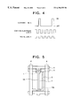
- FIG. 5 is a schematic view showing a structure of a liquid crystal display panel according to a second embodiment of the present invention.
- FIG. 6 is a circuit diagram showing an equivalent circuit of a fundamental pixel unit in the second embodiment.
- FIG. 7 is a schematic view showing a structure of a liquid crystal display panel according to a third embodiment of the present invention.
- FIG. 2 is a schematic view showing a structure of a liquid crystal display panel according a first embodiment of the present invention.
- FIG. 3 is a circuit diagram showing an equivalent circuit of a fundamental pixel unit in the first embodiment.
- a liquid crystal display panel of the embodiment includes two transparent substrates (not shown) having a pair of sheet polarizers and a liquid crystal layer (not shown) sandwiched by the substrates.
- a plurality of signal lines 4 and a plurality of common electrode lines 6 are disposed on a surface on the liquid crystal layer side of one of the two transparent substrates.
- the signal lines 4 and the common electrode lines 6 are preferably intersected with each other perpendicularly.
- a region surrounded by adjacent signal lines 4 and adjacent common electrode lines 6 is a display section 7 of a fundamental pixel unit.
- An opposite electrode 3 preferably extending in the same direction as the signal lines 4 is provided in a central portion of the display section 7 .
- a scanning line 5 is arranged in the vicinity of one of the common electrode lines 6 of the display section 7 .
- a thin film field effect transistor (TFT) 1 whose gate connected to the scanning line 5 is provided on the transparent substrate.
- the drain of the thin film transistor 1 is connected to the common electrode line 6 and the source thereof is connected to the opposite electrode 3 .
- a pixel electrode 2 which is connected to the other of the two signal lines 4 and extends in the same direction as that of the signal lines 4 .
- the opposite electrode 3 is surrounded by the common electrode lines 6 , the pixel electrode 2 and the other signal lines 4 .
- the fundamental pixel unit thus constructed in such a manner, for example, is repeatedly formed on the one of the two transparent substrates. Further, an external circuit (not shown) which applies voltages, while controlling, to the signal lines 4 , the scanning line 5 and the common electrode line 6 is provided outside the panel.
- a voltage applied to the scanning line 5 is controlled by the external circuit so that an ON voltage is applied when a pixel is selected. That is, a voltage which switches the thin film transistor 1 between an ON state and an OFF state is applied to the scanning line 5 . Thereby, one of a writing state and a holding state of each pixel is selected according to a potential of the scanning line 5 .
- a voltage applied to the common electrode 6 is a voltage which controls a potential of the opposite electrode 3 and constant regardless of a pixel and a display condition.
- a constant potential is applied in the same period as a period in which an ON voltage is applied to the scanning line 5 and control is effected by the external circuit so that a relationship in potential between the scanning line 5 and the common electrode line 6 is reversed for each scanning line 5 .
- a voltage applied to the signal line 4 is controlled by the external circuit, according to a picture displayed on a screen, so that a voltage which is computed from a relationship between an applied voltage and a transmittance in advance is applied to the signal line 4 in a timed manner to application of a voltage to the scanning line 5 for each pixel.
- a voltage is applied to the liquid crystal layer of the fundamental pixel unit by a potential difference between a pair of the pixel electrode 2 and the opposite electrode 3 .
- FIG. 4 is a timing chart showing operation of the liquid crystal display panel according to the first embodiment of the present invention.
- a potential difference between the common electrode line 6 and the signal line 4 is a voltage applied to the liquid crystal portion.
- a potential of the pixel electrode 2 is always equal to a potential of the signal line 4 in a voltage holding state, no wiring to prevent a change in potential of the signal line 4 from influencing a display is necessary. Therefore, it is possible to use an area, which the wiring has conventionally occupied in, as a display region, thereby enabling a wide opening area to be secured. Further, since the signal line 4 is used as an pixel electrode 2 , an area occupied by wiring is reduced as compared with conventional and thereby a region corresponding to unnecessary wiring can also be used as an opening section. Therefore, high luminance can actually be realized.
- FIG. 5 is a schematic view showing a structure of a liquid crystal display panel according to the second embodiment of the present invention.
- FIG. 6 is a circuit diagram showing an equivalent circuit of a fundamental pixel unit of the second embodiment. Incidentally, in the second embodiment shown in FIGS. 5 and 6, the same components as those of the first embodiment shown in FIGS. 2 and 3 are indicated by the same reference numerals and detailed descriptions on them will be omitted.
- an opposite electrode 13 preferably extending in the same direction as that of the signal line 4 is arranged in a central portion of the display section 7 .
- the opposite electrode 13 has a region which is superimposed on a portion of the pixel electrode 2 which the portion is parallel to a common electrode 6 .
- an auxiliary capacitor 13 a which has the portion of the pixel electrode 2 and the portion of the opposite electrode 13 as two electrodes, is formed with the superimposed region.
- FIG. 7 is a schematic view showing a structure of a liquid crystal display panel according to the third embodiment of the present invention.
- the same components as those in the first embodiment as shown in FIG. 2 are indicated by the same reference numerals and detailed descriptions on them are omitted.
- each fundamental pixel unit may be constructed in a similar manner to the first embodiment.
- the common electrode 6 to which the thin film transistor 1 is provided is shared by two fundamental pixel units and the two fundamental pixel units are preferably arranged in axial symmetry with respect to the common electrode line 6 .
- the other common electrode line 6 which is provided in the first embodiment, is not provided in the third embodiment.
- a part of a pixel electrode 2 parallel to the common electrode line 6 is also shared by the two fundamental pixel units adjacent to each other in the direction along which the signal line 4 extends.
- a new fundamental unit is constructed from the two fundamental pixel units adjacent to each other in the direction along which the signal line 4 extends and the new fundamental unit is repeatedly formed on one of two transparent substrates.
- the third embodiment can be applied to the second embodiment.
- a common electrode line can be arranged in a layer above a signal line.
Abstract
Description
Claims (5)
Applications Claiming Priority (2)
| Application Number | Priority Date | Filing Date | Title |
|---|---|---|---|
| JP21002698A JP3156671B2 (en) | 1998-07-24 | 1998-07-24 | LCD panel |
| JP10-210026 | 1998-07-24 |
Publications (1)
| Publication Number | Publication Date |
|---|---|
| US6396555B1 true US6396555B1 (en) | 2002-05-28 |
Family
ID=16582597
Family Applications (1)
| Application Number | Title | Priority Date | Filing Date |
|---|---|---|---|
| US09/359,356 Expired - Lifetime US6396555B1 (en) | 1998-07-24 | 1999-07-21 | LCD panel in which the scanning line and the line connected to the drain of the TFT are parallel |
Country Status (4)
| Country | Link |
|---|---|
| US (1) | US6396555B1 (en) |
| JP (1) | JP3156671B2 (en) |
| KR (1) | KR100342123B1 (en) |
| TW (1) | TW536654B (en) |
Cited By (2)
| Publication number | Priority date | Publication date | Assignee | Title |
|---|---|---|---|---|
| US20150179677A1 (en) * | 2013-12-25 | 2015-06-25 | Shenzhen China Star Optoelectronics Technology Co., Ltd. | Liquid crystal display array substrates and a method for manufacturing the same |
| WO2023004864A1 (en) * | 2021-07-29 | 2023-02-02 | 深圳市华星光电半导体显示技术有限公司 | Display panel and display apparatus |
Families Citing this family (7)
| Publication number | Priority date | Publication date | Assignee | Title |
|---|---|---|---|---|
| KR100895017B1 (en) * | 2002-12-10 | 2009-04-30 | 엘지디스플레이 주식회사 | In plane switching mode liquid crystal display device having improved aperture ratio |
| JP2008262006A (en) * | 2007-04-11 | 2008-10-30 | Nec Lcd Technologies Ltd | Active matrix substrate and liquid crystal panel |
| JP4662494B2 (en) * | 2007-10-16 | 2011-03-30 | 東芝モバイルディスプレイ株式会社 | Liquid crystal display device |
| JP2012234212A (en) * | 2012-09-03 | 2012-11-29 | Nlt Technologies Ltd | Active matrix substrate and liquid crystal panel |
| CN104570523B (en) * | 2015-01-16 | 2018-11-13 | 昆山龙腾光电有限公司 | A kind of array substrate, the forming method of array substrate and liquid crystal display device |
| WO2017046931A1 (en) * | 2015-09-17 | 2017-03-23 | 堺ディスプレイプロダクト株式会社 | Liquid crystal display device |
| CN105867033B (en) * | 2016-06-13 | 2019-06-14 | 厦门天马微电子有限公司 | Array substrate and liquid crystal display panel |
Citations (13)
| Publication number | Priority date | Publication date | Assignee | Title |
|---|---|---|---|---|
| US4678282A (en) * | 1985-02-19 | 1987-07-07 | Ovonic Imaging Systems, Inc. | Active display matrix addressable without crossed lines on any one substrate and method of using the same |
| JPH07128687A (en) | 1993-10-28 | 1995-05-19 | Victor Co Of Japan Ltd | Active matrix type pannel device |
| JPH07239480A (en) | 1994-03-01 | 1995-09-12 | Hitachi Ltd | Liquid crystal display substrate |
| JPH0915650A (en) | 1995-04-28 | 1997-01-17 | Hitachi Ltd | Liquid crystal display device |
| JPH09160073A (en) | 1995-12-12 | 1997-06-20 | Sharp Corp | Liquid crystal display device |
| JPH09171194A (en) | 1995-12-20 | 1997-06-30 | Semiconductor Energy Lab Co Ltd | Liquid crystal electro-optic device |
| JPH09185080A (en) | 1995-12-28 | 1997-07-15 | Semiconductor Energy Lab Co Ltd | Liquid crystal electro-optical device |
| JPH09230380A (en) | 1996-02-27 | 1997-09-05 | Sharp Corp | Active matrix substrate and liquid crystal display device |
| JPH1010494A (en) | 1996-06-24 | 1998-01-16 | Hitachi Ltd | Liquid crystal display device |
| JPH1010570A (en) | 1996-06-21 | 1998-01-16 | Nec Corp | Active matrix liquid crystal display panel |
| US6038007A (en) * | 1996-08-30 | 2000-03-14 | Nec Corporation | In-plane type liquid crystal display apparatus with increased numerical aperture |
| US6052163A (en) * | 1996-04-04 | 2000-04-18 | Frontec Incorporated | Thin film transistor and liquid crystal display device |
| US6271903B1 (en) * | 1997-01-23 | 2001-08-07 | Lg. Philips Lcd Co., Ltd. | Liquid crystal display device having a light shielding matrix |
Family Cites Families (5)
| Publication number | Priority date | Publication date | Assignee | Title |
|---|---|---|---|---|
| JP3465835B2 (en) * | 1995-08-21 | 2003-11-10 | 松下電器産業株式会社 | Active matrix type liquid crystal display |
| JPH0980473A (en) * | 1995-09-08 | 1997-03-28 | Hitachi Ltd | Liquid crystal display element |
| JPH09230311A (en) * | 1995-11-14 | 1997-09-05 | Semiconductor Energy Lab Co Ltd | Display device |
| JP3243185B2 (en) * | 1996-07-15 | 2002-01-07 | 株式会社日立製作所 | Active matrix type liquid crystal display device and driving method thereof |
| JP2845215B2 (en) * | 1996-09-20 | 1999-01-13 | 日本電気株式会社 | Liquid crystal display device and method of manufacturing the same |
-
1998
- 1998-07-24 JP JP21002698A patent/JP3156671B2/en not_active Expired - Fee Related
-
1999
- 1999-07-21 US US09/359,356 patent/US6396555B1/en not_active Expired - Lifetime
- 1999-07-22 TW TW088112578A patent/TW536654B/en not_active IP Right Cessation
- 1999-07-24 KR KR1019990030169A patent/KR100342123B1/en not_active IP Right Cessation
Patent Citations (14)
| Publication number | Priority date | Publication date | Assignee | Title |
|---|---|---|---|---|
| US4678282A (en) * | 1985-02-19 | 1987-07-07 | Ovonic Imaging Systems, Inc. | Active display matrix addressable without crossed lines on any one substrate and method of using the same |
| JPH07128687A (en) | 1993-10-28 | 1995-05-19 | Victor Co Of Japan Ltd | Active matrix type pannel device |
| JPH07239480A (en) | 1994-03-01 | 1995-09-12 | Hitachi Ltd | Liquid crystal display substrate |
| JPH0915650A (en) | 1995-04-28 | 1997-01-17 | Hitachi Ltd | Liquid crystal display device |
| JPH09160073A (en) | 1995-12-12 | 1997-06-20 | Sharp Corp | Liquid crystal display device |
| US5892562A (en) * | 1995-12-20 | 1999-04-06 | Semiconductor Energy Laboratory Co., Ltd. | Liquid crystal electro-optic device |
| JPH09171194A (en) | 1995-12-20 | 1997-06-30 | Semiconductor Energy Lab Co Ltd | Liquid crystal electro-optic device |
| JPH09185080A (en) | 1995-12-28 | 1997-07-15 | Semiconductor Energy Lab Co Ltd | Liquid crystal electro-optical device |
| JPH09230380A (en) | 1996-02-27 | 1997-09-05 | Sharp Corp | Active matrix substrate and liquid crystal display device |
| US6052163A (en) * | 1996-04-04 | 2000-04-18 | Frontec Incorporated | Thin film transistor and liquid crystal display device |
| JPH1010570A (en) | 1996-06-21 | 1998-01-16 | Nec Corp | Active matrix liquid crystal display panel |
| JPH1010494A (en) | 1996-06-24 | 1998-01-16 | Hitachi Ltd | Liquid crystal display device |
| US6038007A (en) * | 1996-08-30 | 2000-03-14 | Nec Corporation | In-plane type liquid crystal display apparatus with increased numerical aperture |
| US6271903B1 (en) * | 1997-01-23 | 2001-08-07 | Lg. Philips Lcd Co., Ltd. | Liquid crystal display device having a light shielding matrix |
Cited By (3)
| Publication number | Priority date | Publication date | Assignee | Title |
|---|---|---|---|---|
| US20150179677A1 (en) * | 2013-12-25 | 2015-06-25 | Shenzhen China Star Optoelectronics Technology Co., Ltd. | Liquid crystal display array substrates and a method for manufacturing the same |
| US9461072B2 (en) * | 2013-12-25 | 2016-10-04 | Shenzhen China Star Optoelectronics Technology Co., Ltd. | Liquid crystal display array substrates and a method for manufacturing the same |
| WO2023004864A1 (en) * | 2021-07-29 | 2023-02-02 | 深圳市华星光电半导体显示技术有限公司 | Display panel and display apparatus |
Also Published As
| Publication number | Publication date |
|---|---|
| KR20000011952A (en) | 2000-02-25 |
| KR100342123B1 (en) | 2002-06-26 |
| JP3156671B2 (en) | 2001-04-16 |
| JP2000047250A (en) | 2000-02-18 |
| TW536654B (en) | 2003-06-11 |
Similar Documents
| Publication | Publication Date | Title |
|---|---|---|
| US5870075A (en) | LCD display with divided pixel electrodes connected separately with respective transistors in one pixel and method of driving which uses detection of movement in video | |
| US7064803B2 (en) | Liquid crystal device, method for driving the same, and electronic apparatus | |
| EP1136873B1 (en) | Liquid crystal display element having controlled storage capacitance | |
| KR100311214B1 (en) | LCD having high aperture ratio and high transmittance | |
| US8179489B2 (en) | Display device | |
| US6654075B1 (en) | Liquid crystal display device and method for fabricating the same | |
| JPH1039328A (en) | Liquid crystal display device | |
| JP3006586B2 (en) | Active matrix type liquid crystal display | |
| US6396555B1 (en) | LCD panel in which the scanning line and the line connected to the drain of the TFT are parallel | |
| KR100531388B1 (en) | Display device | |
| US6947021B2 (en) | Liquid crystal display | |
| JP5068608B2 (en) | Dynamic device array substrate | |
| JPH10274783A (en) | Liquid crystal display device | |
| WO2001081993A1 (en) | Liquid crystal display unit | |
| US20110228206A1 (en) | Liquid crystal device and electronic apparatus | |
| JP2003302648A (en) | Liquid crystal display device | |
| US11347122B2 (en) | Display apparatus | |
| US20090153530A1 (en) | Active device array substrate and method for driving the same | |
| JP5137690B2 (en) | Electro-optical device and electronic apparatus equipped with the same | |
| JPH11288006A (en) | Liquid crystal display device | |
| KR100242446B1 (en) | Tft substrate for lcd | |
| JP3268287B2 (en) | Active matrix display device and projection display device using the same | |
| JP4587063B2 (en) | Display device | |
| JP2002140015A (en) | Liquid crystal display device | |
| JP2002123227A (en) | Active matrix type liquid crystal display device |
Legal Events
| Date | Code | Title | Description |
|---|---|---|---|
| AS | Assignment |
Owner name: NEC CORPORATION, JAPAN Free format text: ASSIGNMENT OF ASSIGNORS INTEREST;ASSIGNOR:HORIE, YOSHITAKA;REEL/FRAME:010128/0378 Effective date: 19990714 |
|
| STCF | Information on status: patent grant |
Free format text: PATENTED CASE |
|
| FEPP | Fee payment procedure |
Free format text: PAYOR NUMBER ASSIGNED (ORIGINAL EVENT CODE: ASPN); ENTITY STATUS OF PATENT OWNER: LARGE ENTITY |
|
| AS | Assignment |
Owner name: NEC LCD TECHNOLOGIES, LTD., JAPAN Free format text: ASSIGNMENT OF ASSIGNORS INTEREST;ASSIGNOR:NEC CORPORATION;REEL/FRAME:014108/0248 Effective date: 20030401 |
|
| FPAY | Fee payment |
Year of fee payment: 4 |
|
| FPAY | Fee payment |
Year of fee payment: 8 |
|
| AS | Assignment |
Owner name: NLT TECHNOLOGIES, LTD., JAPAN Free format text: CHANGE OF NAME;ASSIGNOR:NEC LCD TECHNOLOGIES, LTD.;REEL/FRAME:027188/0738 Effective date: 20110701 |
|
| FPAY | Fee payment |
Year of fee payment: 12 |