US6380606B1 - Locos isolation process using a layered pad nitride and dry field oxidation stack and semiconductor device employing the same - Google Patents
Locos isolation process using a layered pad nitride and dry field oxidation stack and semiconductor device employing the same Download PDFInfo
- Publication number
- US6380606B1 US6380606B1 US09/205,413 US20541398A US6380606B1 US 6380606 B1 US6380606 B1 US 6380606B1 US 20541398 A US20541398 A US 20541398A US 6380606 B1 US6380606 B1 US 6380606B1
- Authority
- US
- United States
- Prior art keywords
- stack
- sublayer
- recited
- thickness
- semiconductor
- Prior art date
- Legal status (The legal status is an assumption and is not a legal conclusion. Google has not performed a legal analysis and makes no representation as to the accuracy of the status listed.)
- Expired - Lifetime
Links
Images

Classifications
-
- H—ELECTRICITY
- H01—ELECTRIC ELEMENTS
- H01L—SEMICONDUCTOR DEVICES NOT COVERED BY CLASS H10
- H01L21/00—Processes or apparatus adapted for the manufacture or treatment of semiconductor or solid state devices or of parts thereof
- H01L21/02—Manufacture or treatment of semiconductor devices or of parts thereof
- H01L21/04—Manufacture or treatment of semiconductor devices or of parts thereof the devices having at least one potential-jump barrier or surface barrier, e.g. PN junction, depletion layer or carrier concentration layer
- H01L21/18—Manufacture or treatment of semiconductor devices or of parts thereof the devices having at least one potential-jump barrier or surface barrier, e.g. PN junction, depletion layer or carrier concentration layer the devices having semiconductor bodies comprising elements of Group IV of the Periodic System or AIIIBV compounds with or without impurities, e.g. doping materials
- H01L21/30—Treatment of semiconductor bodies using processes or apparatus not provided for in groups H01L21/20 - H01L21/26
- H01L21/31—Treatment of semiconductor bodies using processes or apparatus not provided for in groups H01L21/20 - H01L21/26 to form insulating layers thereon, e.g. for masking or by using photolithographic techniques; After treatment of these layers; Selection of materials for these layers
- H01L21/314—Inorganic layers
- H01L21/318—Inorganic layers composed of nitrides
- H01L21/3185—Inorganic layers composed of nitrides of siliconnitrides
-
- H—ELECTRICITY
- H01—ELECTRIC ELEMENTS
- H01L—SEMICONDUCTOR DEVICES NOT COVERED BY CLASS H10
- H01L21/00—Processes or apparatus adapted for the manufacture or treatment of semiconductor or solid state devices or of parts thereof
- H01L21/02—Manufacture or treatment of semiconductor devices or of parts thereof
- H01L21/04—Manufacture or treatment of semiconductor devices or of parts thereof the devices having at least one potential-jump barrier or surface barrier, e.g. PN junction, depletion layer or carrier concentration layer
- H01L21/18—Manufacture or treatment of semiconductor devices or of parts thereof the devices having at least one potential-jump barrier or surface barrier, e.g. PN junction, depletion layer or carrier concentration layer the devices having semiconductor bodies comprising elements of Group IV of the Periodic System or AIIIBV compounds with or without impurities, e.g. doping materials
- H01L21/30—Treatment of semiconductor bodies using processes or apparatus not provided for in groups H01L21/20 - H01L21/26
- H01L21/31—Treatment of semiconductor bodies using processes or apparatus not provided for in groups H01L21/20 - H01L21/26 to form insulating layers thereon, e.g. for masking or by using photolithographic techniques; After treatment of these layers; Selection of materials for these layers
- H01L21/32—Treatment of semiconductor bodies using processes or apparatus not provided for in groups H01L21/20 - H01L21/26 to form insulating layers thereon, e.g. for masking or by using photolithographic techniques; After treatment of these layers; Selection of materials for these layers using masks
-
- H—ELECTRICITY
- H01—ELECTRIC ELEMENTS
- H01L—SEMICONDUCTOR DEVICES NOT COVERED BY CLASS H10
- H01L21/00—Processes or apparatus adapted for the manufacture or treatment of semiconductor or solid state devices or of parts thereof
- H01L21/02—Manufacture or treatment of semiconductor devices or of parts thereof
- H01L21/02104—Forming layers
- H01L21/02107—Forming insulating materials on a substrate
- H01L21/02109—Forming insulating materials on a substrate characterised by the type of layer, e.g. type of material, porous/non-porous, pre-cursors, mixtures or laminates
- H01L21/02112—Forming insulating materials on a substrate characterised by the type of layer, e.g. type of material, porous/non-porous, pre-cursors, mixtures or laminates characterised by the material of the layer
- H01L21/02123—Forming insulating materials on a substrate characterised by the type of layer, e.g. type of material, porous/non-porous, pre-cursors, mixtures or laminates characterised by the material of the layer the material containing silicon
- H01L21/0217—Forming insulating materials on a substrate characterised by the type of layer, e.g. type of material, porous/non-porous, pre-cursors, mixtures or laminates characterised by the material of the layer the material containing silicon the material being a silicon nitride not containing oxygen, e.g. SixNy or SixByNz
-
- H—ELECTRICITY
- H01—ELECTRIC ELEMENTS
- H01L—SEMICONDUCTOR DEVICES NOT COVERED BY CLASS H10
- H01L21/00—Processes or apparatus adapted for the manufacture or treatment of semiconductor or solid state devices or of parts thereof
- H01L21/02—Manufacture or treatment of semiconductor devices or of parts thereof
- H01L21/02104—Forming layers
- H01L21/02107—Forming insulating materials on a substrate
- H01L21/02109—Forming insulating materials on a substrate characterised by the type of layer, e.g. type of material, porous/non-porous, pre-cursors, mixtures or laminates
- H01L21/022—Forming insulating materials on a substrate characterised by the type of layer, e.g. type of material, porous/non-porous, pre-cursors, mixtures or laminates the layer being a laminate, i.e. composed of sublayers, e.g. stacks of alternating high-k metal oxides
-
- H—ELECTRICITY
- H01—ELECTRIC ELEMENTS
- H01L—SEMICONDUCTOR DEVICES NOT COVERED BY CLASS H10
- H01L21/00—Processes or apparatus adapted for the manufacture or treatment of semiconductor or solid state devices or of parts thereof
- H01L21/02—Manufacture or treatment of semiconductor devices or of parts thereof
- H01L21/02104—Forming layers
- H01L21/02107—Forming insulating materials on a substrate
- H01L21/02109—Forming insulating materials on a substrate characterised by the type of layer, e.g. type of material, porous/non-porous, pre-cursors, mixtures or laminates
- H01L21/02205—Forming insulating materials on a substrate characterised by the type of layer, e.g. type of material, porous/non-porous, pre-cursors, mixtures or laminates the layer being characterised by the precursor material for deposition
- H01L21/02208—Forming insulating materials on a substrate characterised by the type of layer, e.g. type of material, porous/non-porous, pre-cursors, mixtures or laminates the layer being characterised by the precursor material for deposition the precursor containing a compound comprising Si
- H01L21/02211—Forming insulating materials on a substrate characterised by the type of layer, e.g. type of material, porous/non-porous, pre-cursors, mixtures or laminates the layer being characterised by the precursor material for deposition the precursor containing a compound comprising Si the compound being a silane, e.g. disilane, methylsilane or chlorosilane
-
- H—ELECTRICITY
- H01—ELECTRIC ELEMENTS
- H01L—SEMICONDUCTOR DEVICES NOT COVERED BY CLASS H10
- H01L21/00—Processes or apparatus adapted for the manufacture or treatment of semiconductor or solid state devices or of parts thereof
- H01L21/02—Manufacture or treatment of semiconductor devices or of parts thereof
- H01L21/02104—Forming layers
- H01L21/02107—Forming insulating materials on a substrate
- H01L21/02225—Forming insulating materials on a substrate characterised by the process for the formation of the insulating layer
- H01L21/0226—Forming insulating materials on a substrate characterised by the process for the formation of the insulating layer formation by a deposition process
- H01L21/02263—Forming insulating materials on a substrate characterised by the process for the formation of the insulating layer formation by a deposition process deposition from the gas or vapour phase
- H01L21/02271—Forming insulating materials on a substrate characterised by the process for the formation of the insulating layer formation by a deposition process deposition from the gas or vapour phase deposition by decomposition or reaction of gaseous or vapour phase compounds, i.e. chemical vapour deposition
Definitions
- the present invention is directed, in general, to semiconductor fabrication and, more specifically, to a method of manufacturing a silicon nitride stack and a semiconductor device employing the stack produced by way of the method.
- LOCS Local oxidation of silicon
- Si 3 N 4 silicon nitride
- pad oxide is inserted between the nitride and silicon substrate
- VLSI very large-scale integrated
- LOCOS refers to selective oxidation in device isolation spaces while leaving active device areas unoxidized. The active device area is protected from oxidation by low-pressure chemical vapor deposition (LPCVD) deposited nitride hard masking.
- LPCVD low-pressure chemical vapor deposition
- Poly buffered LOCOS (PBL) utilizes polysilicon or amorphous silicon ( ⁇ -Si) as a buffer between the pad oxide and masking nitride to prevent stress-induced defects. This application of polysilicon allows thinner pad oxide and thicker nitride.
- LOCOS and its derivatives have been remarkably successful in meeting device isolation requirements for metal oxide semiconductors (MOS) technologies developed and manufactured over the last twenty years.
- MOS metal oxide semiconductors
- MOSFET metal oxide semiconductor field effect transistor
- a “bird's-beak” is formed, which partially extends under the nitride layer.
- Bird's beak encroachment refers to lateral oxidation encroachment due to lateral oxygen diffusion beneath the masking nitride, forming the shape of a bird's beak.
- the encroachment reduces the effective size of the device active regions, thus limiting further scale down.
- Bird's beak encroachment is measured from the edge of the masking nitride to the end of oxidation beneath the nitride.
- the bird's-beak produces stress to the nitride layer resulting in nitride lifting and micro-cracks. Therefore, a stress nonuniformity in the nitride layer always exists.
- the thicknesses of the FOX and PADOX have also decreased.
- the FOX thickness has decreased to about 400 nm and below and the PADOX thickness has decreased to about 1.5 nm.
- LOCOS processes using steam FOX have become less desirable because of the harmful effects of the bird's-beak.
- the extension of the bird's-beak under the nitride layer causes oxide/nitride stack lifting.
- Stress within the nitride layer generated during nitride deposition coupled with stress acquired from bird's beak encroachment results in uneven stress distribution within the nitride layer, causing the nitride layer to etch unevenly.
- This uneven etching is highly undesirable because the FOX's thickness is now 400 nm or less, and the large FOX thickness loss during wet etching results in severe compromise on isolation.
- the effects of the bird's-beak with respect to the non-uniform etching of the nitride layer is exacerbated by the facts that conventional deposition processes produce a nitride layer that has a thickness variability of 10% or greater, and the PADOX layers in present day semiconductor devices are around 10.0 nm thick versus the 20 nm thickness found in former technologies. Because of this high thickness variability in the nitride layer and the thinness of the PADOX, the PADOX layer may be inadvertently etched through during the removal of the nitride layer. If the PADOX layer is penetrated and the etch proceeds into the substrate, the semiconductor device may be damaged and may have to be discarded. Therefore, it is highly desirable that the nitride layer have minimum stress and thickness variability for uniform nitride removal with minimum FOX loss and PADOX punch through.
- Field oxide thinning refers to the oxidation growth rate difference between submicron isolation spacing and limited spacing (>1.0 ⁇ m) in the same wafer.
- the oxidation growth rate in isolation spaces 21 1.0 ⁇ m may achieve the targeted oxide thickness, while the growth rate in the submicron area is significantly suppressed.
- the thinning effect is significantly increased as isolation space decreases. This effect poses significant challenges to effective device isolation and smooth surface topology for sub-0.5- ⁇ m technologies. Accordingly, minimization of field oxide thinning is essential.
- Still further processes have involved forming a thicker PADOX.
- this proposed process produces a problem, which only amplifies the above-discussed problems.
- the problem is that the thicker PADOX simply increases the bird's beak length, which, in turn, increases the amount of stress in the nitride layer.
- the increased stress within the nitride layer increases the etch variability of the nitride layer, which, in turn, increases the possibility of puncturing the PADOX.
- the present invention provides methods of manufacturing an isolation structure over a substrate such as that typically found in semiconductors.
- the method includes the steps of: (1) depositing a first stack-nitride sublayer over the substrate at a first deposition rate and (2) subsequently depositing a second stack-nitride sublayer over the first stack-sublayer at a second deposition rate that is different from the first deposition rate.
- the first and second deposition rates provide first and second stack-sublayers that cooperate to form a uniform thickness of the isolation structure over the substrate and provide a stress-accommodating system within the isolation structure.
- the first deposition rate preferably ranges from about 0.5 nm per minute to about 1 nm per minute and the second rate of deposition preferably ranges from about 3 nm per minute to about 5 nm per minute.
- the present invention therefore introduces a method of manufacturing a relatively uniform isolation structure having multiple nitride sublayers.
- the varying rates of deposition, and in some embodiments, accompanying changes in mixture ratio, as well as pressure changes produce a nitride stack that is better able to absorb stress, has greater uniformity and is far less subject to the disadvantageous phenomenon of stack lifting, particularly encountered in semiconductor having a PADOX layer deposited thereon.
- FIG. 1 illustrates a schematic representation of a exemplary structure according to an advantageous embodiment of the present invention, having a nitride layer structure formed over a pad oxide on the surface of a semiconductor substrate;
- FIG. 2 illustrates a schematic graph of a flow rate history for an oxidation scheme in accordance with an advantageous embodiment of the present invention
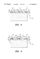
- FIG. 3 illustrates a schematic representation of the exemplary structure of FIG. 1 wherein a portion of the nitride layer structure has been etched away;
- FIG. 4 illustrates a schematic representation of the exemplary structure of FIG. 3 wherein the field oxide has been grown following the etch away of a portion of the nitride layer structure.
- the semiconductor wafer 10 is comprised of a substrate 12 , which has been doped in accordance with conventional processes. While it is preferred that the substrate 12 is comprised of silicon, it will be recognized that other materials, whether presently known or later-determined, may also be used for such manufacture in place of the silicon.
- a pad oxide, PADOX 14 has been formed over the surface of the substrate 12 .
- the PADOX 14 is preferably thermally grown by conventional processes from the substrate 12 itself and is silicon dioxide (SiO 2 ) in exemplary embodiments.
- the thickness of the PADOX 14 may range from about 5 nm to about 25 nm. However, in an exemplary embodiment, the thickness is less than about 6.5 nm, which is considerably thinner than pad oxide thickness of prior art processes and devices. As previously explained, the thickness of the PADOX 14 is a factor in determining the isolation integrity (e.g., bird's-beak length and stack lifting), which is a significant factor in minimizing the stress effects of the bird's-beak formed during the field oxide (FOX) formation. If the PADOX 14 is thicker, there is an increase in the bird's-beak length and thus, the stress. Therefore, it is advantageous to reduce the thickness of the PADOX 14 .
- the isolation integrity e.g., bird's-beak length and stack lifting
- the bird's-beak length achieved lengths as much as about 85 nm. Due to the advantages associated with the present invention, however, it is believed that a bird's-beak length of less than 50 nm can be achieved, which will substantially reduce the amount of stress formed within the FOX isolation structure that is formed over the PADOX 14 .
- the desirable thickness of the PADOX 14 is a function of the thickness variability of the FOX isolation structure and the etch selectivity of that structure and may be mathematically expressed as follows: 2 ⁇ /etch selectivity ⁇ PADOX thickness, where ⁇ is the thickness variability.
- the desired thickness of the PADOX 14 may be determined by simply knowing the thickness variability and the etch selectivity of the FOX isolation structure.
- an isolation structure 16 formed over the PADOX 14 , which is used to isolate the field oxide during its deformation.
- the isolation structure 16 may comprise two layers 16 a and 16 b.
- the isolation structure 16 may comprise at least a third layer 16 c with the overall thickness of the isolation structure 16 having a thickness that ranges between 3 nm and 120 nm.
- an isolation structure comprised of more than three layers is also within the scope of the present invention. In fact, it is believed that the greater the number of layers, the greater the stress reducing capabilities of the isolation structure 16 , as long as the layers do not extend the overall thickness beyond desired parameters.
- the isolation structure 16 is attained by a deliberate oscillation in deposition rate, which is discussed in more detail below. It is expected that this oscillatory deposition scheme creates sublayers within the isolation structure 16 that forms virtual interfaces to accommodate stress and hence minimize pinholes, thickness variability and micro-crack nucleation and propagation. Each layer is successively formed over the other at a rate different than the one before it.
- the first isolation stack-sublayer 16 a is deposited at a first deposition rate, for example 1 nm per minute, and the second isolation stack-sublayer 16 b is then deposited over the first stack-sublayer 16 a at a second deposition rate that is different from the first deposition rate, for example 2 nm per minute.
- its deposition rate is preferably equal to the deposition rate of the first isolation stack-sublayer 16 a.
- the first and second deposition rates provide first and second isolation stack-sublayers 16 a, 16 b that cooperate to form a uniform thickness of the isolation structure 16 over the PADOX 14 and provide a stress-accommodating system within the isolation structure 16 . It is believed that this oscillatory deposition rate scheme produces virtual interfaces 18 between the layers 16 a, 16 b and 16 c. As stated above, it is believed that it is these virtual interfaces 18 that form the stress-accommodating system within the isolation structure 16 .
- the present invention therefore introduces a method of manufacturing a relatively thin field oxide isolation structure having multiple sublayers.
- the varying rates of deposition, and in some embodiments, accompanying changes in mixture ratio, is believed to produce a structure that is better able to absorb stress, has greater uniformity and is less subject to the disadvantageous phenomenon of stack lifting, particularly encountered in semiconductor having a PADOX layer deposited thereon.
- the isolation structure 16 is comprised of a silicon nitride that is composed of a mixture of ammonia (NH 3 ) and dichlorosilane SiCl 2 H 2 or DCS of a predetermined ratio, which is deposited by conventional processes with the exception, of course, of the oscillatory deposition rate scheme proposed by the present invention.
- the NH 3 and DCS is mixed in such a way to produce a hydrogen rich environment.
- the mixture may be mixed to provide a silicon rich environment.
- the predetermined ratio for the first (and, preferably, the third also) isolation stack-sublayers 16 a, 16 c, respectively is about 6:1 (ammonia to dichlorosilane).
- the predetermined ratio for the second isolation stack-sublayer is about 3:1 (ammonia to dichlorosilane), and in yet another embodiment, the predetermined ratio of ammonia to dichlorosilane may be about 12:1.
- the predetermined ratios for these layers may be reversed.
- the predetermined ratio for the isolation stack-sublayers 16 a and 16 c may be about 3:1 and the predetermined ratio for isolation stack-sublayer 16 b may be about 6:1.
- the preferred deposition rate scheme is the former of these examples. It will also, of course, be appreciated that the predetermined ratios may take on a variety of patterns and at a variety of rates, provided that the deposition of each layer is varied from the one previous to it.
- FIG. 2 there is illustrated a schematic graph of the flow rate history for an oxidation scheme in accordance with an advantageous embodiment of the present invention.
- the semiconductor wafer 10 is moved into the deposition chamber.
- An ammonia and dichlorosilane gas mixture is injected into the chamber at a rate of approximately 180 cc per minute for the ammonia and at a rate of approximately 30 cc per minute for the dichlorosilane, which provides a ratio of ammonia to dichlorosilane of about 6:1.
- the temperature and pressure are maintained at approximately 800° C. and about 50 milliTorr, respectively.
- the deposition rate of the silicon nitride may vary greatly.
- the deposition rate may range from about 0.5 nm per minute to about be about 1 nm, which continues until t 2 .
- the period of time that the deposition continues depends on the desired thickness of the first layer.
- the temperatures and pressures at which deposition occurs may also vary, depending on the deposition equipment used and rate of deposition desired.
- first isolation stack-sublayer of silicon nitride having a thickness that varies, depending on the desired application.
- the first stack-sublayer has a thickness that may range from about 1 nm to about 40 nm. In a more specific embodiment, the first stack-sublayer has a thickness of less than about 2 nm. In an even more specific embodiment, the first stack-sublayer has a thickness of about 1.5 nm.
- the temperature is increased from about 800° C. to about 850° C. and the pressure is increased to about 225 milliTorr until t 3 .
- the rate at which the temperature is increase is inconsequential to the overall process. It may be increased rapidly or gradually.
- the ammonia and dichlorosilane gas mixture is injected into the chamber at a rate of about 180 cc per minute for the ammonia and at a rate of about 60 cc per minute for the dichlorosilane, which provides a preferred ratio of ammonia to dichlorosilane of about 3:1.
- the deposition rate of the silicon nitride may vary greatly. For example, the deposition rate may be range from about 3 nm per minute to about 5 nm per minute. This deposition continues until t 4 , which depends on the desired thickness of the second layer.
- second isolation stack-sublayer of silicon nitride having a thickness that varies, depending on the desired application.
- the second stack-sublayer has a thickness-that ranges from about 1 nm to about 40 nm.
- the second isolation stack-sublayer has a thickness of about 2.5 nm.
- the temperature is decreased to about 800° C. until t 5 .
- the rate at which the temperature is increase is inconsequential to the overall process. It may be increased rapidly or gradually.
- the ammonia and dichlorosilane gas mixture is injected into the chamber at a rate of about 180 cc per minute for the ammonia and at a rate of about 30 cc per minute for the dichlorosilane, which provides a preferred ratio of ammonia to dichlorosilane of about 6:1.
- the temperature is maintained at about 800° C. and the pressure is reduced back to about 50 milliTorr.
- the deposition rate of the silicon nitride may vary greatly.
- the deposition rate may range from about 0.5 nm per minute to about 1 nm per minute, which continues until t 6 , at which time, the semiconductor wafer 10 is removed from the deposition chamber.
- the period of time that the deposition continues depends on the desired thickness of the first layer.
- third isolation stack-sublayer of silicon nitride having a thickness that varies, depending on the application.
- the thickness of the third isolation stack-sublayer may range from about 1 nm to about 40 nm.
- the above-described process may be repeated for several cycles that are limited only by the overall thickness requirements of the semiconductor.
- FIG. 3 there is illustrated an intermediate structure of the semiconductor wafer 10 manufactured in accordance with the present invention.
- the isolation structure 16 has been masked and etched in accordance with conventional processes.
- the above-described process produces an isolation structure that is better able to absorb stress, has greater uniformity and is far less subject to the disadvantageous phenomenon of stack lifting, particularly encountered in semiconductors having a PADOX layer deposited thereon.
- the uniformity in thickness provides an isolation structure that, in preferred embodiments, has thickness variability of less than three percent. This excellent thickness variability allows the PADOX 14 to be much thinner than before since the thickness produced by the present process is extremely uniform across the semiconductor wafer 10 .
- the oscillatory fashion in which the isolation layers 16 a, 16 b and 16 c are deposited provide a isolation structure 16 that has virtual interfaces 18 therebetween to accommodate and reduce the overall stress within the isolation structure 16 .
- FIG. 4 there is illustrated the semiconductor wafer 10 of FIG. 3 wherein a field oxide 20 has been isolated and formed on the semiconductor wafer 10 and between the isolation structures 16 .
- the field oxide 20 can be grown with conventional dry oxide process, which reduces the bird's-beak length and thereby reduces the stack-lifting. This reduced stack-lifting, in turn, also reduces the stress within the isolation structure 16 .
- a bird's-beak length of less than 50 nm can be achieved by way of the deposition method provided by the present invention with a field oxide thinning of less than 25 nm.
- the reduction in stress provides a isolation structure that etches more evenly.
- the PADOX's thickness may also be reduced, thereby achieving a reduction in the overall thickness of the semiconductor device.
- the starting substrate was a p/p + (100) and the silicon wafers were oxidized at 800° C. to 850° C. to form the buffer PADOX having a thickness ranging from about 5 nm to 20 nm.
- the PADOX was capped with a nitride layer having a thickness ranging from about 60 nm to about 120 nm and composed for three deposited stack-sublayers.
- the nitride layers were deposited by low pressure chemical vapor deposition (LPCVD) by a reaction of ammonia (NH 3 ) and dichlorosilane SiH 2 Cl 2 .
- the unique isolation structure of the present invention was obtained by a deliberate oscillation in the deposition rate of the various stack-sublayers (1 nm to 5 nm/minute) by fluctuating the NH 3 :SiH 2 Cl 2 ratio from about 6:1 to about 3:1 and the pressure from about 50 to about 250 milliTorr during the LPCVD reaction of NH 3 and SiH 2 Cl 2 at about 750° C. to about 800° C., as discussed above. It is believed that this fluctuation in deposition rate causes microstructural sublayering. At least two stack-sublayers are needed for stress-accommodation and reduction. In addition, decreasing the ammonia:dichlorosilane ratio also makes the isolation structure silicon rich. It is further believed that the oscillatory fashion in which the pad silicon nitride isolation structure is formed produces an isolation structure that has thickness and stress unformity, which are important to the isolation integrity.
- Forming the stack-sublayers as discussed herein achieved an isolation structure thickness variability from wafer to wafer of less than 2% with stress accommodation and stress reduction. Thus, there was better etch selectivity with no stack lifting, and a thinner PADOX of less than 6.5 nm was used without oxide punch through.
- Pad oxides with thicknesses ranging from about 5 nm to about 15 nm and pad nitride (isolation structure) with thicknesses ranging from about 60 nm to about 120 nm for a dry field oxide with a thickness ranging from about 100 nm to about 250 nm were fabricated. The results are shown in the following tables:
- the present invention provides a process and a semiconductor that has the advantages of: (1) reduced isolation structure thickness variability, (2)oscillatory layering that results in stress accommodation and reduction with a simultaneous reduction in pinholes and micro-cracks, (3) better etch selectivity of the isolation structure is expected due to stress accommodation, (4)PADOX thickness reduction to 5 nm and (5) reduction of stack-lifting due to stress accommodation.
Abstract
Description
| Birds Beak Length (Pad Oxide = 9 nm) |
| FOX thickness | 150 | nm | 200 | nm | 250 | nm |
| 117.5 nm Si3N4 | 25 | nm | 40 | nm | 50 | nm |
| 240 nm Si3N4 | 25 | nm | 40 | nm | 50 | nm |
| Birds Beak Length (FOX = 250 nm) |
| Pad-Oxide Thickness | 9 | nm | 15 |
20 nm | ||
| 117.5 nm Si3N4 | 50 | nm | 65 nm | 80 nm | ||
| 240 nm Si3N4 | 50 | nm | 65 nm | 70 nm | ||
| Birds Beak Length (FOX = 250 nm) |
| Si3N4 Thickness | 117.5 | nm | 180 | nm | 240 | nm |
| 9 nm Pad-Oxide | 50 | nm | 50 | nm | 50 | |
| 20 nm Pad-Oxide | 89 | nm | 80 | nm | 80 | nm |
Claims (23)
Priority Applications (1)
| Application Number | Priority Date | Filing Date | Title |
|---|---|---|---|
| US09/205,413 US6380606B1 (en) | 1997-06-18 | 1998-12-02 | Locos isolation process using a layered pad nitride and dry field oxidation stack and semiconductor device employing the same |
Applications Claiming Priority (2)
| Application Number | Priority Date | Filing Date | Title |
|---|---|---|---|
| US08/878,242 US6090686A (en) | 1997-06-18 | 1997-06-18 | Locos isolation process using a layered pad nitride and dry field oxidation stack and semiconductor device employing the same |
| US09/205,413 US6380606B1 (en) | 1997-06-18 | 1998-12-02 | Locos isolation process using a layered pad nitride and dry field oxidation stack and semiconductor device employing the same |
Related Parent Applications (1)
| Application Number | Title | Priority Date | Filing Date |
|---|---|---|---|
| US08/878,242 Division US6090686A (en) | 1997-06-18 | 1997-06-18 | Locos isolation process using a layered pad nitride and dry field oxidation stack and semiconductor device employing the same |
Publications (1)
| Publication Number | Publication Date |
|---|---|
| US6380606B1 true US6380606B1 (en) | 2002-04-30 |
Family
ID=25371650
Family Applications (2)
| Application Number | Title | Priority Date | Filing Date |
|---|---|---|---|
| US08/878,242 Expired - Lifetime US6090686A (en) | 1997-06-18 | 1997-06-18 | Locos isolation process using a layered pad nitride and dry field oxidation stack and semiconductor device employing the same |
| US09/205,413 Expired - Lifetime US6380606B1 (en) | 1997-06-18 | 1998-12-02 | Locos isolation process using a layered pad nitride and dry field oxidation stack and semiconductor device employing the same |
Family Applications Before (1)
| Application Number | Title | Priority Date | Filing Date |
|---|---|---|---|
| US08/878,242 Expired - Lifetime US6090686A (en) | 1997-06-18 | 1997-06-18 | Locos isolation process using a layered pad nitride and dry field oxidation stack and semiconductor device employing the same |
Country Status (4)
| Country | Link |
|---|---|
| US (2) | US6090686A (en) |
| EP (1) | EP0886309A1 (en) |
| JP (1) | JPH1174265A (en) |
| KR (1) | KR19990007078A (en) |
Cited By (2)
| Publication number | Priority date | Publication date | Assignee | Title |
|---|---|---|---|---|
| US6566183B1 (en) * | 2001-12-12 | 2003-05-20 | Steven A. Chen | Method of making a transistor, in particular spacers of the transistor |
| US6747338B1 (en) | 2002-11-27 | 2004-06-08 | Analog Devices, Inc. | Composite dielectric with improved etch selectivity for high voltage MEMS structures |
Families Citing this family (8)
| Publication number | Priority date | Publication date | Assignee | Title |
|---|---|---|---|---|
| US5712186A (en) * | 1996-06-12 | 1998-01-27 | Micron Technology, Inc. | Method for growing field oxide to minimize birds' beak length |
| US6051511A (en) | 1997-07-31 | 2000-04-18 | Micron Technology, Inc. | Method and apparatus for reducing isolation stress in integrated circuits |
| US6239003B1 (en) * | 1998-06-16 | 2001-05-29 | Texas Instruments Incorporated | Method of simultaneous fabrication of isolation and gate regions in a semiconductor device |
| KR100340716B1 (en) * | 1999-10-29 | 2002-06-20 | 윤종용 | method for forming silicion nitride |
| US6171948B1 (en) * | 1999-11-02 | 2001-01-09 | Micron Technology, Inc. | Method for filling structural gaps and intergrated circuitry |
| US6599798B2 (en) * | 2001-07-24 | 2003-07-29 | Infineon Technologies Ag | Method of preparing buried LOCOS collar in trench DRAMS |
| US6717226B2 (en) * | 2002-03-15 | 2004-04-06 | Motorola, Inc. | Transistor with layered high-K gate dielectric and method therefor |
| US6949448B2 (en) * | 2003-04-01 | 2005-09-27 | Taiwan Semiconductor Manufacturing Co., Ltd. | Local oxidation of silicon (LOCOS) method employing graded oxidation mask |
Citations (19)
| Publication number | Priority date | Publication date | Assignee | Title |
|---|---|---|---|---|
| US3874919A (en) | 1974-03-13 | 1975-04-01 | Ibm | Oxidation resistant mask layer and process for producing recessed oxide region in a silicon body |
| US3925804A (en) * | 1974-01-29 | 1975-12-09 | Westinghouse Electric Corp | Structure of and the method of processing a semiconductor matrix or MNOS memory elements |
| US4110899A (en) | 1976-01-12 | 1978-09-05 | Hitachi, Ltd. | Method for manufacturing complementary insulated gate field effect transistors |
| US4268321A (en) | 1978-08-23 | 1981-05-19 | Hitachi, Ltd. | Method of fabricating a semiconductor device having channel stoppers |
| US4333964A (en) | 1980-09-15 | 1982-06-08 | General Electric Company | Method of making integrated circuits |
| US4398992A (en) | 1982-05-20 | 1983-08-16 | Hewlett-Packard Company | Defect free zero oxide encroachment process for semiconductor fabrication |
| JPS618929A (en) | 1984-06-22 | 1986-01-16 | Matsushita Electric Ind Co Ltd | Formation of thin film |
| US4631804A (en) | 1984-12-10 | 1986-12-30 | At&T Bell Laboratories | Technique for reducing substrate warpage springback using a polysilicon subsurface strained layer |
| US4729816A (en) | 1987-01-02 | 1988-03-08 | Motorola, Inc. | Isolation formation process with active area protection |
| US5153701A (en) | 1987-12-28 | 1992-10-06 | At&T Bell Laboratories | Semiconductor device with low defect density oxide |
| JPH0669499A (en) | 1992-08-20 | 1994-03-11 | Matsushita Electron Corp | Manufacture of mos-structure transistor |
| US5306946A (en) | 1990-10-15 | 1994-04-26 | Seiko Epson Corporation | Semiconductor device having a passivation layer with silicon nitride layers |
| US5441768A (en) | 1994-02-08 | 1995-08-15 | Applied Materials, Inc. | Multi-step chemical vapor deposition method for thin film transistors |
| US5472906A (en) | 1993-12-08 | 1995-12-05 | Matsushita Electric Industrial Co., Ltd. | Method of forming isolation |
| US5539249A (en) * | 1993-07-06 | 1996-07-23 | Motorola, Inc. | Method and structure for forming an integrated circuit pattern on a semiconductor substrate |
| US5679600A (en) | 1995-10-11 | 1997-10-21 | Micron Technology, Inc. | Double locos for submicron isolation |
| US5763317A (en) * | 1995-12-30 | 1998-06-09 | Hyundai Electronics Industries Co., Ltd. | Method for PBLOCOS isolation between semiconductor devices |
| US5981403A (en) * | 1997-11-24 | 1999-11-09 | Lucent Technologies, Inc. | Layered silicon nitride deposition process |
| US6051496A (en) * | 1998-09-17 | 2000-04-18 | Taiwan Semiconductor Manufacturing Company | Use of stop layer for chemical mechanical polishing of CU damascene |
-
1997
- 1997-06-18 US US08/878,242 patent/US6090686A/en not_active Expired - Lifetime
-
1998
- 1998-06-09 EP EP98304526A patent/EP0886309A1/en not_active Withdrawn
- 1998-06-17 JP JP10169774A patent/JPH1174265A/en active Pending
- 1998-06-18 KR KR1019980022855A patent/KR19990007078A/en active IP Right Grant
- 1998-12-02 US US09/205,413 patent/US6380606B1/en not_active Expired - Lifetime
Patent Citations (19)
| Publication number | Priority date | Publication date | Assignee | Title |
|---|---|---|---|---|
| US3925804A (en) * | 1974-01-29 | 1975-12-09 | Westinghouse Electric Corp | Structure of and the method of processing a semiconductor matrix or MNOS memory elements |
| US3874919A (en) | 1974-03-13 | 1975-04-01 | Ibm | Oxidation resistant mask layer and process for producing recessed oxide region in a silicon body |
| US4110899A (en) | 1976-01-12 | 1978-09-05 | Hitachi, Ltd. | Method for manufacturing complementary insulated gate field effect transistors |
| US4268321A (en) | 1978-08-23 | 1981-05-19 | Hitachi, Ltd. | Method of fabricating a semiconductor device having channel stoppers |
| US4333964A (en) | 1980-09-15 | 1982-06-08 | General Electric Company | Method of making integrated circuits |
| US4398992A (en) | 1982-05-20 | 1983-08-16 | Hewlett-Packard Company | Defect free zero oxide encroachment process for semiconductor fabrication |
| JPS618929A (en) | 1984-06-22 | 1986-01-16 | Matsushita Electric Ind Co Ltd | Formation of thin film |
| US4631804A (en) | 1984-12-10 | 1986-12-30 | At&T Bell Laboratories | Technique for reducing substrate warpage springback using a polysilicon subsurface strained layer |
| US4729816A (en) | 1987-01-02 | 1988-03-08 | Motorola, Inc. | Isolation formation process with active area protection |
| US5153701A (en) | 1987-12-28 | 1992-10-06 | At&T Bell Laboratories | Semiconductor device with low defect density oxide |
| US5306946A (en) | 1990-10-15 | 1994-04-26 | Seiko Epson Corporation | Semiconductor device having a passivation layer with silicon nitride layers |
| JPH0669499A (en) | 1992-08-20 | 1994-03-11 | Matsushita Electron Corp | Manufacture of mos-structure transistor |
| US5539249A (en) * | 1993-07-06 | 1996-07-23 | Motorola, Inc. | Method and structure for forming an integrated circuit pattern on a semiconductor substrate |
| US5472906A (en) | 1993-12-08 | 1995-12-05 | Matsushita Electric Industrial Co., Ltd. | Method of forming isolation |
| US5441768A (en) | 1994-02-08 | 1995-08-15 | Applied Materials, Inc. | Multi-step chemical vapor deposition method for thin film transistors |
| US5679600A (en) | 1995-10-11 | 1997-10-21 | Micron Technology, Inc. | Double locos for submicron isolation |
| US5763317A (en) * | 1995-12-30 | 1998-06-09 | Hyundai Electronics Industries Co., Ltd. | Method for PBLOCOS isolation between semiconductor devices |
| US5981403A (en) * | 1997-11-24 | 1999-11-09 | Lucent Technologies, Inc. | Layered silicon nitride deposition process |
| US6051496A (en) * | 1998-09-17 | 2000-04-18 | Taiwan Semiconductor Manufacturing Company | Use of stop layer for chemical mechanical polishing of CU damascene |
Non-Patent Citations (19)
| Title |
|---|
| Gary DePinto and Jim Wilson: "Optimization of LPCVD Silicon Nitride Deposition Process by Use of Designed Experiments"; IEEE Advanced Semiconductor Manufacturing Conference; Sep. 11-12, 1990; pp. 47-53. |
| H. W. van Zeijl. L. K. Nanver P. J. French; Low-Stress Nitride As Oxidation Ask for Submicrometre Locos Isolation; IEEE Electron Device Letters; May 25, 1995: pp. 927-929. |
| H.W. van Zeijl, L. K. Nanver and P. J. French, "Low-stress nitride as oxidation mask for submicrometre LOCOS isolation", May 25, 1995-vol. 31-No. 11-Electronics Letters, (p. 927). |
| Hong-Hsiang Tsai, Chin-Lin Yu and Ching-Yuan Wu, "A New Twin-Well CMOs Process Using Nitridized-Oxide-LOCOS (NOLOCOS) Isolation Technology", 1989 IEEE, (p. 307). |
| J. D. Bude, M. Mastrapasqua, M.R. Pinto, R.W. Gregor, P.J. Kelley, R.A. Kohler, C.W. Leung, Ma, R.J. McPartland, P.K. Roy and R. Singh, "Secondary Electron Flash-A High Performance, Low Power Flash Technology for 0.35 mum and Below," 1997 IEEE, pp. 11.3.1-11.3.4. |
| J. D. Bude, M. Mastrapasqua, M.R. Pinto, R.W. Gregor, P.J. Kelley, R.A. Kohler, C.W. Leung, Ma, R.J. McPartland, P.K. Roy and R. Singh, "Secondary Electron Flash—A High Performance, Low Power Flash Technology for 0.35 μm and Below," 1997 IEEE, pp. 11.3.1—11.3.4. |
| J.R. Pfiester, P.U. Kenkare, R. Subrahmanyan, J.H. Lin and P. Crabtree: "Nitride-Clad Locos Isolation for 0.25mum CMOS"; Digest of Technical Papers of the Symposium on VLSI Technology; May 17, 1993: pp. 139-140. |
| J.R. Pfiester, P.U. Kenkare, R. Subrahmanyan, J.H. Lin and P. Crabtree: "Nitride-Clad Locos Isolation for 0.25μm CMOS"; Digest of Technical Papers of the Symposium on VLSI Technology; May 17, 1993: pp. 139-140. |
| Koji Suzuki, Kazunobu Mameno, Hideharu Nagasawa, Atsuhiro Nishida, Hideaki Fujiwara Kiyoshi Yoneda, "Half-Micron LOCOS Isolation Using High Energy Ion Implantation", Sep. 1992-IEICE Trans. Electron vol. E75C. No. 9 (pp. 972-977). |
| M. Ghezzo, E. Kaminsky, Y. Nissan-Cohen, P. Frank and R. Saia, "LOPOS: Advanced Device Isolation for a 0.8 mum CMOS/Bulk Process Technology", Jul. 1989-vol. 136-No. 7 Journal of the Electrochemical Society, (pp. 1992-1996). |
| M. Ghezzo, E. Kaminsky, Y. Nissan-Cohen, P. Frank and R. Saia, "LOPOS: Advanced Device Isolation for a 0.8 μm CMOS/Bulk Process Technology", Jul. 1989-vol. 136-No. 7 Journal of the Electrochemical Society, (pp. 1992-1996). |
| N. Guillemot, Georges Pananakakis and Pierre Chenevier, A New Analytical Model of the "Bird's Beak", 1987 IEEE, (pp. 1033-1038. |
| Peter I.L. Smeys, Peter B. Griffin and Krishna C. Saraswat; "Material Properties or Low Pressure Chemical Vapor Deposited Silicon Nitride for Modeling and Calibrating the Simulation of Advanced Isolation Structures"; Journal of Applied Physics; Aug. 15, 1995; pp. 2837-2842. |
| Q.W. Ren, L.K. Nanver, C. R. de Boer and H.W. van Zeijl; "Silicon Nitride as Dielectric in the Low Temperature SiGe HBT Processing"; Microelectronic Engineering 36 (1997); pp. 179-182. |
| Sang S. Kim, Alan Emani & Simon Deleonibus, "High-pressure and high-temperature furnace oxidation for advanced poly-buffered Locos", Nov. 1994-Solid State Technology, (pp. 67-72). |
| Seiichi Mori, Eiji Sakagami, Hitoshi Araki, Yukio Kaneko, Kazuhito Narita, Yoichi Ohshima, Norihisa Arai and Kuniyoshi Yoshikawa, "Ono Inter-Poly Dielectric Scaling for Nonvolatile Memory Applications," IEEE Transactions on Electron Devices, vol. 38, No. 2, Feb. 1991, pp. 386-390. |
| Seiichi Mori, Yoshiko Yamaguchi Araki, Muneharu Sato, Hisataka Meguro, Hiroaki Tsunoda, Eiji Kamiya, Kuniyoshi Yoshikawa, Norihisa Arai, and Eiji Sakagami, "Thickness Scaling Limitation Factors of Ono Interpoly Dielectric for Nonvolatile Memory Devices," IEEE Transactions on Electron Devices, vol. 43, No. 1, Jan. 1996, pp. 47-53. |
| Stanley Wofd, "A Review of IC Isolation Technologies-Part 6", Dec. 1992-Solid State Technology, (pp. 39-41). |
| Stanley Wolf, "A Review of IC Isolation Technologies-Part 5", Nov. 1992-Solid State Technology, (pp. 47-48). |
Cited By (2)
| Publication number | Priority date | Publication date | Assignee | Title |
|---|---|---|---|---|
| US6566183B1 (en) * | 2001-12-12 | 2003-05-20 | Steven A. Chen | Method of making a transistor, in particular spacers of the transistor |
| US6747338B1 (en) | 2002-11-27 | 2004-06-08 | Analog Devices, Inc. | Composite dielectric with improved etch selectivity for high voltage MEMS structures |
Also Published As
| Publication number | Publication date |
|---|---|
| US6090686A (en) | 2000-07-18 |
| EP0886309A1 (en) | 1998-12-23 |
| KR19990007078A (en) | 1999-01-25 |
| JPH1174265A (en) | 1999-03-16 |
Similar Documents
| Publication | Publication Date | Title |
|---|---|---|
| US6414376B1 (en) | Method and apparatus for reducing isolation stress in integrated circuits | |
| US6544875B1 (en) | Chemical vapor deposition of silicate high dielectric constant materials | |
| US5151381A (en) | Method for local oxidation of silicon employing two oxidation steps | |
| US6080682A (en) | Methodology for achieving dual gate oxide thicknesses | |
| US6008106A (en) | Micro-trench oxidation by using rough oxide mask for field isolation | |
| KR20000069813A (en) | N2o nitrided-oxide trench sidewals to prevent boron outdiffusion and decrease stress | |
| US6100160A (en) | Oxide etch barrier formed by nitridation | |
| US5858852A (en) | Fabrication process of a stack type semiconductor capacitive element | |
| US6380606B1 (en) | Locos isolation process using a layered pad nitride and dry field oxidation stack and semiconductor device employing the same | |
| US20020151142A1 (en) | Thermally stable poly-Si/high dielectric constant material interfaces | |
| KR20030011186A (en) | Method of forming gete electrode in semiconductor device and method of forming cell gete electrode in non-volatile memory device by using the same | |
| KR100206029B1 (en) | Manufacture of semiconductor device | |
| KR100381961B1 (en) | Method for forming a nitridized interface on a semiconductor substrate | |
| JPH09326391A (en) | Manufacture of element isolation oxide film | |
| JP2538830B2 (en) | A method for partial oxidation of silicon using a ceramic barrier layer. | |
| US5804492A (en) | Method of fabricating an isolation region for semiconductor device | |
| US5726091A (en) | Method of reducing bird's beak of field oxide using reoxidized nitrided pad oxide layer | |
| US6197662B1 (en) | Semiconductor processing method of forming field isolation oxide using a polybuffered mask which includes a base nitride layer on the substrate, and other semiconductor processing methods | |
| KR100256264B1 (en) | Semiconductor elenent field oxidation layer manufacturing method | |
| KR960009985B1 (en) | Manufacturing method of silicon oxide with removed bird's beak in fully recessed local oxidation | |
| KR100310463B1 (en) | Method for forming isolation layer of semiconductor device | |
| KR100399972B1 (en) | Method for forming isolation layer of semiconductor device | |
| JPH0817814A (en) | Method for forming oxidation prevention film for separating element | |
| KR100226214B1 (en) | Method of fabricating gate isolation film of semiconductor device | |
| KR960010461B1 (en) | Manufacturing method of field oxide in semiconductor device |
Legal Events
| Date | Code | Title | Description |
|---|---|---|---|
| AS | Assignment |
Owner name: LUCENT TECHNOLOGIES INC., NEW JERSEY Free format text: ASSIGNMENT OF ASSIGNORS INTEREST;ASSIGNORS:BRADY, DAVID C.;KIZILYALLI, ISIK C.;ROY, PRADIP K.;AND OTHERS;REEL/FRAME:009621/0687;SIGNING DATES FROM 19970428 TO 19970616 |
|
| STCF | Information on status: patent grant |
Free format text: PATENTED CASE |
|
| FEPP | Fee payment procedure |
Free format text: PAYOR NUMBER ASSIGNED (ORIGINAL EVENT CODE: ASPN); ENTITY STATUS OF PATENT OWNER: LARGE ENTITY |
|
| FPAY | Fee payment |
Year of fee payment: 4 |
|
| FPAY | Fee payment |
Year of fee payment: 8 |
|
| FPAY | Fee payment |
Year of fee payment: 12 |
|
| AS | Assignment |
Owner name: DEUTSCHE BANK AG NEW YORK BRANCH, AS COLLATERAL AG Free format text: PATENT SECURITY AGREEMENT;ASSIGNORS:LSI CORPORATION;AGERE SYSTEMS LLC;REEL/FRAME:032856/0031 Effective date: 20140506 |
|
| AS | Assignment |
Owner name: AVAGO TECHNOLOGIES GENERAL IP (SINGAPORE) PTE. LTD Free format text: ASSIGNMENT OF ASSIGNORS INTEREST;ASSIGNOR:AGERE SYSTEMS LLC;REEL/FRAME:035365/0634 Effective date: 20140804 |
|
| AS | Assignment |
Owner name: LSI CORPORATION, CALIFORNIA Free format text: TERMINATION AND RELEASE OF SECURITY INTEREST IN PATENT RIGHTS (RELEASES RF 032856-0031);ASSIGNOR:DEUTSCHE BANK AG NEW YORK BRANCH, AS COLLATERAL AGENT;REEL/FRAME:037684/0039 Effective date: 20160201 Owner name: AGERE SYSTEMS LLC, PENNSYLVANIA Free format text: TERMINATION AND RELEASE OF SECURITY INTEREST IN PATENT RIGHTS (RELEASES RF 032856-0031);ASSIGNOR:DEUTSCHE BANK AG NEW YORK BRANCH, AS COLLATERAL AGENT;REEL/FRAME:037684/0039 Effective date: 20160201 |
|
| AS | Assignment |
Owner name: BANK OF AMERICA, N.A., AS COLLATERAL AGENT, NORTH CAROLINA Free format text: PATENT SECURITY AGREEMENT;ASSIGNOR:AVAGO TECHNOLOGIES GENERAL IP (SINGAPORE) PTE. LTD.;REEL/FRAME:037808/0001 Effective date: 20160201 Owner name: BANK OF AMERICA, N.A., AS COLLATERAL AGENT, NORTH Free format text: PATENT SECURITY AGREEMENT;ASSIGNOR:AVAGO TECHNOLOGIES GENERAL IP (SINGAPORE) PTE. LTD.;REEL/FRAME:037808/0001 Effective date: 20160201 |
|
| AS | Assignment |
Owner name: AVAGO TECHNOLOGIES GENERAL IP (SINGAPORE) PTE. LTD., SINGAPORE Free format text: TERMINATION AND RELEASE OF SECURITY INTEREST IN PATENTS;ASSIGNOR:BANK OF AMERICA, N.A., AS COLLATERAL AGENT;REEL/FRAME:041710/0001 Effective date: 20170119 Owner name: AVAGO TECHNOLOGIES GENERAL IP (SINGAPORE) PTE. LTD Free format text: TERMINATION AND RELEASE OF SECURITY INTEREST IN PATENTS;ASSIGNOR:BANK OF AMERICA, N.A., AS COLLATERAL AGENT;REEL/FRAME:041710/0001 Effective date: 20170119 |
|
| AS | Assignment |
Owner name: BELL SEMICONDUCTOR, LLC, ILLINOIS Free format text: ASSIGNMENT OF ASSIGNORS INTEREST;ASSIGNORS:AVAGO TECHNOLOGIES GENERAL IP (SINGAPORE) PTE. LTD.;BROADCOM CORPORATION;REEL/FRAME:044886/0608 Effective date: 20171208 |
|
| AS | Assignment |
Owner name: CORTLAND CAPITAL MARKET SERVICES LLC, AS COLLATERA Free format text: SECURITY INTEREST;ASSIGNORS:HILCO PATENT ACQUISITION 56, LLC;BELL SEMICONDUCTOR, LLC;BELL NORTHERN RESEARCH, LLC;REEL/FRAME:045216/0020 Effective date: 20180124 |
|
| AS | Assignment |
Owner name: BELL NORTHERN RESEARCH, LLC, ILLINOIS Free format text: RELEASE BY SECURED PARTY;ASSIGNOR:CORTLAND CAPITAL MARKET SERVICES LLC;REEL/FRAME:059720/0719 Effective date: 20220401 Owner name: BELL SEMICONDUCTOR, LLC, ILLINOIS Free format text: RELEASE BY SECURED PARTY;ASSIGNOR:CORTLAND CAPITAL MARKET SERVICES LLC;REEL/FRAME:059720/0719 Effective date: 20220401 Owner name: HILCO PATENT ACQUISITION 56, LLC, ILLINOIS Free format text: RELEASE BY SECURED PARTY;ASSIGNOR:CORTLAND CAPITAL MARKET SERVICES LLC;REEL/FRAME:059720/0719 Effective date: 20220401 |