US6302959B2 - Mn2+ activated green emitting SrAl12O19 luminescent material - Google Patents
Mn2+ activated green emitting SrAl12O19 luminescent material Download PDFInfo
- Publication number
- US6302959B2 US6302959B2 US09/748,777 US74877700A US6302959B2 US 6302959 B2 US6302959 B2 US 6302959B2 US 74877700 A US74877700 A US 74877700A US 6302959 B2 US6302959 B2 US 6302959B2
- Authority
- US
- United States
- Prior art keywords
- phosphor
- ions
- seed
- scintillator
- temperature zone
- Prior art date
- Legal status (The legal status is an assumption and is not a legal conclusion. Google has not performed a legal analysis and makes no representation as to the accuracy of the status listed.)
- Expired - Fee Related
Links
Images


Classifications
-
- H—ELECTRICITY
- H01—ELECTRIC ELEMENTS
- H01J—ELECTRIC DISCHARGE TUBES OR DISCHARGE LAMPS
- H01J61/00—Gas-discharge or vapour-discharge lamps
- H01J61/02—Details
- H01J61/38—Devices for influencing the colour or wavelength of the light
- H01J61/42—Devices for influencing the colour or wavelength of the light by transforming the wavelength of the light by luminescence
- H01J61/44—Devices characterised by the luminescent material
-
- C—CHEMISTRY; METALLURGY
- C09—DYES; PAINTS; POLISHES; NATURAL RESINS; ADHESIVES; COMPOSITIONS NOT OTHERWISE PROVIDED FOR; APPLICATIONS OF MATERIALS NOT OTHERWISE PROVIDED FOR
- C09K—MATERIALS FOR MISCELLANEOUS APPLICATIONS, NOT PROVIDED FOR ELSEWHERE
- C09K11/00—Luminescent, e.g. electroluminescent, chemiluminescent materials
- C09K11/08—Luminescent, e.g. electroluminescent, chemiluminescent materials containing inorganic luminescent materials
- C09K11/77—Luminescent, e.g. electroluminescent, chemiluminescent materials containing inorganic luminescent materials containing rare earth metals
- C09K11/7701—Chalogenides
- C09K11/7703—Chalogenides with alkaline earth metals
-
- C—CHEMISTRY; METALLURGY
- C09—DYES; PAINTS; POLISHES; NATURAL RESINS; ADHESIVES; COMPOSITIONS NOT OTHERWISE PROVIDED FOR; APPLICATIONS OF MATERIALS NOT OTHERWISE PROVIDED FOR
- C09K—MATERIALS FOR MISCELLANEOUS APPLICATIONS, NOT PROVIDED FOR ELSEWHERE
- C09K11/00—Luminescent, e.g. electroluminescent, chemiluminescent materials
- C09K11/08—Luminescent, e.g. electroluminescent, chemiluminescent materials containing inorganic luminescent materials
- C09K11/77—Luminescent, e.g. electroluminescent, chemiluminescent materials containing inorganic luminescent materials containing rare earth metals
- C09K11/7712—Borates
-
- C—CHEMISTRY; METALLURGY
- C09—DYES; PAINTS; POLISHES; NATURAL RESINS; ADHESIVES; COMPOSITIONS NOT OTHERWISE PROVIDED FOR; APPLICATIONS OF MATERIALS NOT OTHERWISE PROVIDED FOR
- C09K—MATERIALS FOR MISCELLANEOUS APPLICATIONS, NOT PROVIDED FOR ELSEWHERE
- C09K11/00—Luminescent, e.g. electroluminescent, chemiluminescent materials
- C09K11/08—Luminescent, e.g. electroluminescent, chemiluminescent materials containing inorganic luminescent materials
- C09K11/77—Luminescent, e.g. electroluminescent, chemiluminescent materials containing inorganic luminescent materials containing rare earth metals
- C09K11/7766—Luminescent, e.g. electroluminescent, chemiluminescent materials containing inorganic luminescent materials containing rare earth metals containing two or more rare earth metals
- C09K11/7774—Aluminates
-
- H—ELECTRICITY
- H01—ELECTRIC ELEMENTS
- H01J—ELECTRIC DISCHARGE TUBES OR DISCHARGE LAMPS
- H01J29/00—Details of cathode-ray tubes or of electron-beam tubes of the types covered by group H01J31/00
- H01J29/02—Electrodes; Screens; Mounting, supporting, spacing or insulating thereof
- H01J29/10—Screens on or from which an image or pattern is formed, picked up, converted or stored
- H01J29/18—Luminescent screens
- H01J29/20—Luminescent screens characterised by the luminescent material
-
- G—PHYSICS
- G21—NUCLEAR PHYSICS; NUCLEAR ENGINEERING
- G21K—TECHNIQUES FOR HANDLING PARTICLES OR IONISING RADIATION NOT OTHERWISE PROVIDED FOR; IRRADIATION DEVICES; GAMMA RAY OR X-RAY MICROSCOPES
- G21K4/00—Conversion screens for the conversion of the spatial distribution of X-rays or particle radiation into visible images, e.g. fluoroscopic screens
- G21K2004/06—Conversion screens for the conversion of the spatial distribution of X-rays or particle radiation into visible images, e.g. fluoroscopic screens with a phosphor layer
Definitions
- the present invention is directed to a luminescent material doped with various ions, and more particularly to a SrAl 12 O 19 material doped with Mn 2+ Ce 3+ , Pr 3+ , Gd 3+ , Tb 3+ and/or Mg 2+ and used as a lamp phosphor, a display phosphor or as a laser crystal.
- a luminescent material absorbs energy in one portion of the electromagnetic spectrum and emits energy in another portion of the electromagnetic spectrum.
- a luminescent material in powder form is commonly called a phosphor, while a luminescent material in the form of a transparent solid body is commonly called a scintillator.
- phosphors and scintillators emit radiation in the visible portion of the spectrum in response to the absorption of radiation which is outside the visible portion of the spectrum.
- the phosphor performs the function of converting electromagnetic radiation to which the human eye is not sensitive into electromagnetic radiation to which the human eye is sensitive.
- Most phosphors are responsive to more energetic portions of the electromagnetic spectrum than the visible portion of the spectrum.
- luminescent materials Two broad classes of luminescent materials are recognized. These are self-activated luminescent materials and impurity-activated luminescent materials.
- a self-activated luminescent material is one in which the pure crystalline host material upon absorption of a high energy photon elevates electrons to an excited state from which they return to a lower energy state by emitting a photon.
- Self-activated luminescent materials normally have a broad spectrum emission pattern because of the relatively wide range of energies which the electron may have in either the excited or the lower energy states. Thus, any given excited electron may emit a fairly wide range of energy during its transition from its excited to its lower energy state, depending on the particular energies it has before and after its emissive transition.
- An impurity activated luminescent material is normally one in which a non-luminescent host material has been modified by inclusion of an activator species which is present in the host material in a relatively low concentration, such as in the range from about 200 parts per million to 1,000 parts per million. However, some materials require several mole or atomic percent of activator ions for optimized light output. With an impurity activated luminescent material, the activator ions may directly absorb the incident photons or the lattice may absorb the incident photons and transfer the absorbed photon energy to the activator ions.
- the photon absorbed by the lattice may create mobile migrating electrons and holes in the lattice. Due to favorable charge configurations, the migrating electrons and holes are trapped at the activator ions, where they recombine and emit a photon of luminescent light.
- the photon if the photon is absorbed directly by the activator ion, the photon raises one or more electrons of the activator ion to a more excited state. These electrons, in returning to their less excited state, emit a photon of luminescent light.
- the electrons which emit the luminescent light are d or f shell electrons whose energy levels may be significantly affected or relatively unaffected, respectively, by the surrounding crystal field.
- the emitted luminescent light is substantially characteristic of the activator ions rather than the host material and the luminescent spectrum comprises one or more relatively narrow emission peaks. This contrasts with a self-activated luminescent material's much broader emission spectrum.
- the host lattice When a host lattice absorbs the incident photon (i.e. the excitation energy) and transfers it to the activator ion, the host lattice acts as a sensitizer.
- the host lattice may also be doped with sensitizer atoms.
- the sensitizer atoms absorb the incident photon either directly, or from the host lattice, and transfer it to the activator ion.
- One prior art green light emitting phosphor is Zn 2 SiO 4 :Mn 2+ .
- This phosphor is used in display devices, such as plasma displays and cathode ray tubes (CRT), and in various fluorescent lamps.
- the phosphor absorbs the emitted UV radiation from the lamp or plasma display or electrons in a CRT and emits radiation in the green spectral range.
- a phosphor It is generally advantageous for a phosphor to be resistant to radiation damage and exhibit a high lumen maintenance.
- Radiation damage is the characteristic of a luminescent material in which the quantity of light emitted by the luminescent material in response to a given intensity of stimulating radiation decreases after the material has been exposed to a high radiation does.
- Lumen maintenance is the ability of a luminescent material to resist radiation damage over time. Luminescent materials with a high resistance to radiation damage over time have a high lumen maintenance.
- the Zn 2 SiO 4 :Mn 2+ phosphor has shown a significant decrease in light output after several hundred hours of bombardment by energetic UV radiation or electrons. Therefore, the phosphor suffers from poor lumen maintenance.
- One embodiment of the present invention provides a composition of matter, comprising AD 12 O 19 :Mn,R where A comprises at least one of strontium, barium and calcium, D comprises at least one of aluminum, gallium, boron and magnesium and R comprises at least one trivalent rare earth ion.
- a luminescent device comprising a housing, a source of energetic media contained in the housing and a luminescent material contained in the interior of the housing.
- the luminescent material comprises AD 12 O 19 :Mn,R where A comprises at least one of strontium, barium and calcium, D comprises at least one of aluminum, gallium, boron and magnesium and R comprises at least one trivalent rare earth ion.
- an embodiment of the present invention provides a method of making a phosphor, comprising the steps of mixing oxide, carbonate, hydroxide, nitrate or oxalate compounds of strontium, aluminum, manganese and at least one of gallium, magnesium, boron, calcium, barium, cerium, praseodymium, gadolinium and terbium, and heating a resulting mixture to form the phosphor.
- An embodiment of the present invention also provides a method of making a scintillator, comprising the steps of placing a single crystal seed in contact with a melt comprising strontium, aluminum, oxygen, maganese and at least one of gallium, magnesium, boron, calcium, barium, cerium, praseodymium, gadolinium and terbium, moving the seed from a high temperature zone to a low temperature zone and forming a single crystal scintillator in contact with the seed.
- FIG. 1 is a perspective view of a magnetoplumbite crystal structure.
- FIG. 2 is side cross sectional view of a fluorescent lamp coated with a phosphor in accordance with an exemplary embodiment of the present invention.
- FIGS. 3 and 4 are side cross sectional view of cathode ray tubes coated with a phosphor in accordance with an exemplary embodiment of the present invention.
- FIG. 5 is a side cross sectional view of a liquid crystal display device coated with a phosphor in accordance with an exemplary embodiment of the present invention.
- FIG. 6 is a side cross sectional view of a plasma display device coated with a phosphor in accordance with an exemplary embodiment of the present invention.
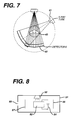
- FIG. 7 is a side cross sectional view of an X-ray detection device containing a scintillator in accordance with an exemplary embodiment of the present invention.
- FIG. 8 a side cross sectional view of a laser containing a scintillator in accordance with an exemplary embodiment of the present invention.
- FIG. 9 is a schematic of one method of making a scintillator in accordance with an exemplary embodiment of the present invention.
- FIG. 10 is a schematic of another method of making a scintillator in accordance with an exemplary embodiment of the present invention.
- FIG. 11 is comparison of emission spectra of the phosphor in accordance with an exemplary embodiment of the present invention and of a prior art phosphor under 254 nm incident radiation.
- FIG. 12 is comparison of chromaticity color coordinates of the phosphor of an exemplary embodiment of the present invention and of a prior art phosphor.
- SrAl 12 O 19 is a luminescent material in the green spectral range when it is doped with Mn 2+ activator ions. Furthermore, trivalent rare earth ions, such as Ce, Pr, Gd and Tb act as sensitizers in SrAl 12 O 19 :Mn 2+ . This material has a more saturated green luminescence (i.e., a sharp emission peak with a maximum wavelength in the green spectral region) and an equivalent absolute quantum efficiency compared to the prior art Zn 2 SiO 4 :Mn 2+ phosphor, having a broad emission peak in the green-yellow spectral range.
- trivalent rare earth ions such as Ce, Pr, Gd and Tb act as sensitizers in SrAl 12 O 19 :Mn 2+ .
- This material has a more saturated green luminescence (i.e., a sharp emission peak with a maximum wavelength in the green spectral region) and an equivalent absolute quantum efficiency compared to the prior art Zn 2 SiO
- the SrAl 12 O 19 :Mn 2+ phosphor is also superior to the Zn 2 SiO 4 :Mn 2+ phosphor with respect to high energy radiation damage resistance and lumen maintenance because of an inherent stability of its magnetoplumbite lattice structure.
- the SrAl 12 O 19 material crystallizes in a magnetoplumbite structure, as shown in FIG. 1 .
- the Mn 2+ dopant ions substitute Al ions on the Al tetrahedral cation sites not occupying the mirror plane. Therefore, the Mn ions have a tetrahedral coordination because each Mn ion has four bonds. Tetrahedrally coordinated Mn 2+ ions are subject to a weak crystal field. Therefore, SrAl 12 O 19 :Mn 2+ emits radiation in the green spectral range because the emitted luminescent light is substantially characteristic of the Mn 2+ activator ions rather than of the host material.
- the strontium ions occupy cation sites inside the magnetoplumbite lattice mirror plane. Therefore, these ions expand the lattice mirror plane and are a source of crystal field effects in the lattice.
- the trivalent rare earth dopant ions occupy the Sr lattice sites. Since the rare earth ions are larger than the Sr ions, the rare earth ions may cause a greater amount of mirror plane expansion than the Sr ions and act as sensitizers for the Mn 2+ activator ions.
- the preferred trivalent rare earth ions are cerium (Ce), praseodymium (Pr), gadolinium (Gd) and terbium (Tb).
- Pr acts as a sensitizer for 185 nm incident radiation. Therefore, if the luminescent material is exposed to 185 nm radiation, the Pr ions on the Sr lattice sites absorb the incident radiation and transfer the energy generated by the incident radiation to the Mn 2+ activator ions on the Al sites. Therefore, if SrAl 12 O 19 :Mn 2+ is used as a green emitting phosphor for a UV gas discharge lamp that emits at 185 nm, then the phosphor should be doped with Pr activator ions.
- Ce acts as a sensitizer for 254 nm incident radiation. Therefore, if the luminescent material is exposed to 254 nm radiation, the Ce ions on the Sr lattice sites absorb the incident radiation and transfer the energy generated by the incident radiation to the Mn 2+ activator ions on the Al sites. Therefore, if SrAl 12 O 19 :Mn 2+ is used as a green emitting phosphor for a UV gas discharge lamp that emits at 254 nm, then the phosphor should be doped with Ce activator ions.
- both Ce and Pr sensitizers should be used. It should be noted that Pr and Ce act as sensitizers for ranges of different wavelengths extending to about 300 nm, and not just for 185 and 254 nm wavelengths.
- the current inventors believe the following possible mechanism of energy transfer utilizing Gd ions.
- the Gd ions reside on adjacent Sr sites in the magnetoplumbite SrAl 12 O 19 lattice to form a Gd ion sublattice.
- the Pr or Ce sensitizers absorb the incident radiation and transfer the energy to at least one Gd ion in the sublattice.
- the Gd ions then transfer the energy to other Gd ions in the sublattice, until the energy reaches a Gd ion adjacent to a Mn 2+ activator.
- the energy is then transferred from the sublattice to the activator.
- the Gd ion sublattice facilitates energy transfer to the activator ions. Therefore, Gd may be added to SrAl 12 O 19 :Mn 2+ in addition to Pr and/or Ce.
- Tb acts as a quantum efficiency enhancer in SrAl 12 O 19 :Mn 2+ .
- the present inventors discovered that when SrAl 12 O 19 :Mn 2+ is doped with Tb ions, the green Mn 2+ quantum efficiency is improved compared to SrAl 12 O 19 :Mn 2+ that is not doped with Tb ions. Therefore, SrAl 12 O 19 :Mn 2+ may be doped with Tb ions in addition to being doped with Pr, Ce and/or Gd ions.
- the current inventors believe that a complex, multistage energy transfer probably occurs when SrAl 12 O 19 :Mn 2+ is doped with Tb ions as well as other trivalent rare earth ions to achieve an improved quantum efficiency.
- the current inventors determined that the green light is emitted mainly from the Mn 2+ ions, and not from the Ce 3+ or Tb 3+ ions in SrAl 12 O 19 :Mn 2+ ,Tb 3+ ,Ce 3 3+ .
- the SrAl 12 O 19 :Mn 2+ material may comprise any combination of one, two, three or four trivalent rare earth ion dopant species, depending on the required use of the material.
- the dopant species comprise Pr, Ce, Gd and Tb.
- Al ions may be replaced by gallium, boron or magnesium ion dopant species.
- a preferred dopant species that substitutes the Al ions are the Mg ions. Mg ions act as charge compensating ions when the Sr 2+ lattice sites are filled by trivalent rare earth ions.
- a portion of the Sr ions may also be replaced by calcium or barium ion dopant species, if desired.
- the luminescent material according to an exemplary embodiment of the present invention may be characterized by the following generic formula: AD 12 O 19 :Mn,R, where A comprises at least one of strontium, calcium and barium, D comprises at least one of aluminum, gallium, boron and magnesium and R comprises at least one trivalent rare earth ion.
- Mn comprises an activator ion with a 2+ valence state.
- Mn ion concentration may range from greater than zero to 50 mode or atomic percent or less of ⁇ fraction (1/12) ⁇ of the D cationic species.
- the preferred Mn ion concentration range is 20 to 30 atomic percent and the preferred Mn ion concentration is 25 atomic percent of ⁇ fraction (1/12) ⁇ of the D cationic species.
- the remaining 11.5 to 12 moles of the D cationic species may comprise Al or a combination of Al and Mg.
- the magnesium ion concentration may range from zero to 50 mole or atomic percent of ⁇ fraction (1/12) ⁇ of the total Al ion concentration.
- the preferred Mg ion concentration range is 20 to 30 atomic percent and the preferred Mg ion concentration is 25 atomic percent of ⁇ fraction (1/12) ⁇ of the Al cationic species.
- R ion concentration may range from greater than zero to 100 mole or atomic percent of the A cationic species (i.e., the strontium cationic species, which may be partially substituted by calcium or barium cationic species, if desired).
- the preferred R ion concentration range is 25 to 75 atomic percent and the preferred R ion concentration is 50 atomic percent of the A cationic species.
- concentrations of Mn and R ions may be expressed by the following formula: (A 1-x R x )(D 12-z Mn z )O 19 where 0 ⁇ X ⁇ 1; 0 ⁇ Z ⁇ 0.5.
- A comprises strontium
- D comprises at least one of aluminum and magnesium
- R comprises at least one of cerium, praseodymium, gadolinium and terbium.
- Cerium and praseodymium ion concentration may range from zero to 100 mole or atomic percent each of the total Sr ion concentration. It should be understood that any combination of Ce and Pr ion concentrations cannot exceed 100 mole of atomic percent of the Sr ion concentration.
- the preferred Ce and Pr ion concentration range is 10 to 40 atomic percent each of the Sr cationic species. If Ce ions are added without adding Pr ions, then the preferred Ce ion concentration is 30 atomic percent of the Sr cationic species. If Pr ions are added without adding Ce ions, then the preferred Pr ion concentration is 30 atomic percent of the Sr cationic species. If both Ce and Pr ions are added, then preferred Ce and Pr ion concentration is 15 atomic percent each of the Sr cationic species.
- Gd and Tb ion concentration may range from zero to 50 mole or atomic percent each of the total Sr ion concentration.
- the preferred Gd and Tb ion concentration range is 5 to 15 atomic percent each and the preferred Gd and Tb ion concentration is 10 atomic percent each of the Sr cationic species.
- concentrations of Mg, Ce, Pr, Gd and Tb ions in the preferred material of the present invention may be expressed by the following formula: (Sr 1-m-q-r-t Ce m Pr q Gd r Tb t )(Al 12-e-g Mg e Mn g )O 19 where 0 ⁇ m ⁇ 1; 0 ⁇ q ⁇ 1; 0 ⁇ r ⁇ 0.5; 0 ⁇ t ⁇ 0.5; 0 ⁇ e ⁇ 0.5; and 0 ⁇ g ⁇ 0.5.
- One preferred material of the present invention contains non-zero concentrations of Mg, Ce, Pr, Gd and Tb ions.
- Another preferred material of the present invention contains non-zero concentrations of at least one of Ce and Pr ions.
- Another preferred material of the present invention contains non-zero concentrations of Ce and at least one of Gd and Tb ions. Yet another preferred material of the present invention contains non-zero concentrations of Pr and at least one of Gd and Tb ions.
- Three specific preferred materials of the present invention are:
- the luminescent material described above may be used in many different applications.
- the material may be used as a phosphor in lamp, in a cathode ray tube, in a plasma display device or in a liquid crystal display.
- the material may also be used as a scintillator in an electromagnetic calorimeter, in a gamma ray camera, in a computed tomography scanner or in a laser. These uses are meant to be merely exemplary and not exhaustive.
- the AD 12 O 19 :Mn,R phosphor may be used in a lamp.
- the phosphor may be used in a linear fluorescent lamp, as shown, for example in FIG. 2.
- a fluorescent lamp comprises a bulb 1 filled with a gas, the phosphor 2 formed on the interior surface of the bulb 1 , plural cathodes or gas discharge electrodes 3 and a lamp cap or base 4 .
- the phosphor 2 may be coated on the outside surface of the bulb 1 , or on a separate envelope containing the gas.
- the bulb 1 is preferably made of glass. Other appropriate transparent materials may also be used.
- the gas such a mercury, emits radiation (i.e. ultraviolet radiation) when a potential is applied to the cathode 3 through the base 4 .
- the phosphor 2 absorbs the incident UV radiation from the gas and emits green light.
- the Ad 12 O 19 :Mn,R phosphor may be used in a cathode ray tube (CRT).
- the phosphor may be used in a CRT adapted for use in a television set, as shown, for example in FIG. 3 .
- the CRT contains at least one, and preferably three electron gun(s) 5 , at least one electron beam deflector 6 , and anode 7 , a display screen 10 and the phosphor 2 coated on the inside of screen.
- the CRT operates by emitting an electron beam 8 from the gun 5 .
- the beam 8 is attracted to the phosphor 2 by the anode 7 .
- the deflectors 6 control the position of the beam 8 on the phosphor 2 .
- the CRT may comprise a cathode array as shown, for example in FIG. 4 .
- the CRT comprises an array of Spindt cathodes 11 (only one cathode is shown for clarity).
- a control circuit (not shown) applies a potential to a particular cathode 11 , it emits an electron beam 8 toward the phosphor 2 .
- the phosphor 2 coverts the electron beam 8 into an emission of green light 9 .
- the AD 12 O 19 :Mn,R phosphor may be used in a liquid crystal display (LCD), such as the one shown, for example, in FIG. 5 .
- the LCD comprises a transparent substrate 12 , a light source 13 , an array of plural control transistors 14 , 15 , such as thin film transistors (only two are shown for clarity), a transparent electrode 16 , 17 in electrical contact with each transistor, liquid crystal material 18 , a transparent counter substrate 19 , the green emitting AD 12 O 19 :Mn,R phosphor 2 formed on the counter substrate 19 above electrode 16 , another phosphor 20 formed on the counter substrate 19 above electrode 17 , a transparent display screen 21 , and an opaque housing 22 .
- the electrode 16 When transistor 14 is switched on, the electrode 16 applies a potential to the liquid crystal material 18 directly above the electrode 16 . The applied potential forces the liquid crystal material 18 to become transparent above electrode 16 . The liquid crystal material remains opaque above electrode 17 if no potential is applied to electrode 17 from transistor 15 . The light from lamp 13 may now pass through the transparent portion of the liquid crystal material 18 to reach the phosphor 2 . Phosphor 2 absorbs the light from lamp 13 and emits green light through screen 21 . An image may be formed on the screen 21 by controlling the transmission of light from lamp 13 to various colored phosphors 2 , 20 through the liquid crystal material. The phosphor 2 may alternatively be formed above counter substrate 19 or on the inside surface of screen 21 .
- the AD 12 O 19 :Mn,R phosphor may be used in a plasma display device, such as the one as shown, for example, in FIG. 6 .
- the plasma display device comprises a transparent display screen 21 , an opaque housing 22 , a gas envelope 23 , an array of gas discharge electrodes 23 (only one electrode is shown for clarity) and a control device 25 , such as a transistor.
- the phosphor 2 may be formed on the interior or exterior surface of the gas envelope 23 or on the interior surface of the screen 21 .
- the control device 25 applies a potential to electrode 24 , the electrode 24 creates a localized plasma discharge in the gas contained in the envelope 23 .
- the localized plasma emits UV radiation that is absorbed by an adjacent portion the phosphor 2 .
- the irradiated portion of the phosphor 2 then emits green light through the screen 21 .
- An image may be formed on the screen 21 by controlling the application of the potential to different electrodes 24 of the electrode array.
- the scintillator of the present invention may be used in a computed tomography (CT) scanning system, as shown in example in FIG. 7 .
- CT scanning system is used to obtain cross sectional images of the human body.
- an X-ray source such as an X-ray tube 41 rotates in a circle about the patient 43 .
- An X-ray detector 42 is placed on the opposite side of the patient 43 .
- the detector 42 rotates synchronously with the X-ray source about the perimeter of the circle.
- the detector comprises the AD 12 O 19 :Mn,R scintillator optically coupled to a photodiode or another type of photodetector.
- the detector 42 may comprise a AD 12 O 19 :Mn,R phosphor coated on a transparent substrate and optically coupled to a photodiode or another type of photodetector.
- the AD 12 O 19 :Mn,R scintillator may comprise a laser crystal, as shown for example in FIG. 8 .
- the laser comprises a housing 51 , the scintillator crystal 52 and a light source, such as a lamp 53 .
- a potential is applied to the crystal 52 thorough electrodes from a voltage source 54 .
- the crystal 52 emits coherent green radiation through aperture 55 while the crystal is irradiated by the light source 53 and a potential is applied from the voltage source 54 .
- the laser may optionally contain a full mirror 56 and a half mirror 57 for amplification of the coherent light amplitude by back and forth reflection of the light between the mirrors.
- the laser crystal 52 may be cleaved and/or processed to form a full mirror surface on the back of the crystal and a partial mirror surface on the front surface of the crystal 52 facing the aperture 55 .
- the AD 12 O 19 :Mn,R scintillator may also be used as a gamma ray camera or an electromagnetic calorimeter.
- a gamma ray camera the scintillator absorbs gamma rays and emits green light to expose a film.
- an electromagnetic calorimeter the scintillator absorbs high energy incident radiation, such as gamma rays collected by a telescope or positrons emitted by a positron source, and emits green light.
- Incident radiation for a distal radiation source enters the housing through an aperture in the housing. In these applications, this aperture may be considered as the source of incident radiation for the scintillator.
- the AD 12 O 19 :Mn,R phosphor and scintillator may be used in applications other than those described above.
- the AD 12 O 19 :Mn,R phosphor may be made by any ceramic powder method, such as a liquid phase (flux) method or a solid state method.
- the method of making the phosphor comprises the following steps. First, compounds of the phosphor material are mixed in a crucible or another suitable container, such as a ball mill.
- the starting materials may be blended using a ball mill with ZrO 2 or yttrium toughened zirconia milling media.
- the preferred starting phosphor compounds comprise oxides, carbonates, hydroxides, nitrates or oxalates of the metal constituents.
- the blended materials are then fired in a reducing atmosphere for 5-15 hours at 1,400 to 1600° C., preferably for 10 hours at 1500° C. to sinter the material.
- the reducing atmosphere may comprise forming gas (2 percent hydrogen and 98 percent nitrogen).
- the starting materials also have a reducing atmosphere for 5-15 hours at 1,400 to 1600° C., preferably for 10 hours at 1500° C. to sinter the material.
- the reducing atmosphere may comprise forming gas (2 percent hydrogen and 98 percent nitrogen).
- the starting materials also have forming gas (2 percent hydrogen and 98 percent nitrogen).
- the ceramic phosphor may contain a flux that promotes the reaction of the starting materials during the firing step to form the ceramic phosphor.
- the flux comprises a halogen compound, such as a fluoride or a chloride compound.
- the preferred halogen compounds comprise magnesium, aluminum or strontium fluoride or magnesium, strontium, manganese or ammonium chloride.
- the phosphor may be fired without adding a flux.
- the fired mixture is then coated onto the substrate, such as a display screen or a lamp bulb.
- a suspension of the mixture particles and a liquid is used to coat the substrate.
- the AD 12 O 19 :Mn,R scintillator may be made by any crystal growth method.
- the scintillator is made by either the Bridgeman-Stockbarger method or the Czochralski method.
- a schematic of the Bridgeman-Stockbarger crystal growth method is shown in FIG. 9.
- a solid AD 12 O 19 :Mn,R material is placed in contact with a single crystal seed 61 in a housing or container.
- the seed 61 may comprise AD 12 O 19 :Mn,R or another material with a magnetoplumbite crystal structure.
- the solid material is then placed into a high temperature zone 62 .
- the high temperature zone may comprise a resistance or lamp heater.
- the heater may have a bar or strip shape that melts only a portion of the solid material or it may be a furnace that melts the entire solid material to form a melt region 64 .
- the seed 61 and the melt region 64 are then moved into a low temperature zone 63 . If the high temperature zone 62 comprises a bar shaped heater, then the low temperature zone 63 comprises the area away from the heater. If the high temperature zone 62 comprises a furnace, then the low temperature zone 63 may be an area outside the furnace or a second furnace set to a lower temperature than the first furnace.
- the two furnaces are preferably separated by an insulating material 65 .
- the melt region 64 When the melt region 64 reaches the low temperature zone, it solidifies as a single crystal 66 that has the same lattice and orientation as the seed 61 .
- the seed and the solid material may be moved relative to a stationary heater or furnace. Alternatively, the heater or furnace may be moved relative to a stationary seed 61 . The relative movement may be vertical, horizontal or in any other direction.
- FIG. 10 A schematic of the Czochralski crystal growth method is shown in FIG. 10 .
- the starting materials comprising strontium, aluminum, oxygen, and at least one of magnesium, manganese, gallium, boron, barium, calcium, cerium, praseodymium, gadolinium and terbium are placed in a crucible 71 and heated to form a reactant melt 72 .
- the crucible is located in a housing, such as a quartz tube 73 , and heated by r.f. or resistance heaters 74 .
- the melt temperature is determined by a thermocouple 75 .
- a single crystal seed 76 attached to a seed holder 77 is lowered into the melt (the melt is the high temperature zone).
- a single crystal scintillator boule 78 forms below the seed.
- the size of the crystal boule 78 increases as the seed 76 is lifted further away from the melt 72 toward the low temperature zone above the heaters 74 .
- the boule is then sliced and polished into scintillator crystals.
- the (Sr 0.5 Ce 0.3 Gd 0.1 Tb 0.1 )(Al 11.5 Mg 0.25 Mn 0.25 )O 19 phosphor of the present invention and a Zn 2 SiO 4 :Mn 2+ prior art phosphor were irradiated with 254 nm incident radiation, and their emission spectra were measured with a spectrometer. The spectra are shown in FIG. 11 .
- the (Sr 0.5 Ce 0.3 Gd 0.1 Tb 0.1 )(Al 11.5 Mg 0.25 Mn 0.25 )O 19 phosphor exhibited a maximum emission wavelength of 517 nm. This wavelength in the green spectral range is only 6 nm away from the Zn 2 SiO 4 :Mn 2+ maximum emission wavelength of 523 nm.
- the chromaticity color coordinates x and y are known in the phosphor art, and are defined for example in a textbook by K. H. Butler, “ Fluorescent Lamp Phosphors, Technology and Theory” (Penn State U. Press 1980), pages 98-107.
- the solid curve in the diagram shows the monochromatic emission wavelength corresponding to certain x and y coordinates. As seen in FIG.
- the (Sr 0.5 Ce 0.3 Gd 0.1 Tb 0.1 )(Al 11.5 Mg 0.25 Mn 0.25 )O 19 phosphor (filled-in circle 81 ) which has a peak emission wavelength in the green range, has a more saturated green luminescence than the prior art Zn 2 SiO 4 :Mn 2+ phosphor (open circle 82 ) which has a peak emission wavelength in the green-yellow range. Furthermore, the two phosphors have an equivalent absolute quantum efficiency. Therefore, the AD 12 O 19 :Mn,R phosphor may replace the Zn 2 SiO 4 :Mn 2+ phosphor in virtually all applications. It should be understood that the example above is meant to merely illustrate the present invention and should not be deemed as limiting the scope of the claims.
Abstract
A SrAl12O19 green luminescent material is doped with Mn2+ activator ions and at least one trivalent rare earth sensitizer ion species. Preferably, the material contains four rare earth ions: Ce3+, Pr3+, Gd3+ and Tb3+. Optionally, a portion of the aluminum may be substituted with magnesium. The material may be used as a display device or lamp phosphor or as an X-ray diagnostic or laster scintillator.
Description
This application is division of application Ser. No. 09/359,900, filed Jul. 26, 1999, which is hereby incorporated by reference in its entirety.
The present invention is directed to a luminescent material doped with various ions, and more particularly to a SrAl12O19 material doped with Mn2+ Ce3+, Pr3+, Gd3+, Tb3+ and/or Mg2+ and used as a lamp phosphor, a display phosphor or as a laser crystal.
A luminescent material absorbs energy in one portion of the electromagnetic spectrum and emits energy in another portion of the electromagnetic spectrum. A luminescent material in powder form is commonly called a phosphor, while a luminescent material in the form of a transparent solid body is commonly called a scintillator.
Most useful phosphors and scintillators emit radiation in the visible portion of the spectrum in response to the absorption of radiation which is outside the visible portion of the spectrum. Thus, the phosphor performs the function of converting electromagnetic radiation to which the human eye is not sensitive into electromagnetic radiation to which the human eye is sensitive. Most phosphors are responsive to more energetic portions of the electromagnetic spectrum than the visible portion of the spectrum. Thus, there are phosphors and scintillators which are responsive to ultraviolet light (as in fluorescent lamps), electrons (as in cathode ray tubes) and x-rays (as in radiography).
Two broad classes of luminescent materials are recognized. These are self-activated luminescent materials and impurity-activated luminescent materials.
A self-activated luminescent material is one in which the pure crystalline host material upon absorption of a high energy photon elevates electrons to an excited state from which they return to a lower energy state by emitting a photon. Self-activated luminescent materials normally have a broad spectrum emission pattern because of the relatively wide range of energies which the electron may have in either the excited or the lower energy states. Thus, any given excited electron may emit a fairly wide range of energy during its transition from its excited to its lower energy state, depending on the particular energies it has before and after its emissive transition.
An impurity activated luminescent material is normally one in which a non-luminescent host material has been modified by inclusion of an activator species which is present in the host material in a relatively low concentration, such as in the range from about 200 parts per million to 1,000 parts per million. However, some materials require several mole or atomic percent of activator ions for optimized light output. With an impurity activated luminescent material, the activator ions may directly absorb the incident photons or the lattice may absorb the incident photons and transfer the absorbed photon energy to the activator ions.
The photon absorbed by the lattice may create mobile migrating electrons and holes in the lattice. Due to favorable charge configurations, the migrating electrons and holes are trapped at the activator ions, where they recombine and emit a photon of luminescent light.
Alternatively, if the photon is absorbed directly by the activator ion, the photon raises one or more electrons of the activator ion to a more excited state. These electrons, in returning to their less excited state, emit a photon of luminescent light.
In many commonly employed impurity activated luminescent materials, the electrons which emit the luminescent light are d or f shell electrons whose energy levels may be significantly affected or relatively unaffected, respectively, by the surrounding crystal field. In those situations where the activator ion is not much affect by the local crystal field, the emitted luminescent light is substantially characteristic of the activator ions rather than the host material and the luminescent spectrum comprises one or more relatively narrow emission peaks. This contrasts with a self-activated luminescent material's much broader emission spectrum.
When a host lattice absorbs the incident photon (i.e. the excitation energy) and transfers it to the activator ion, the host lattice acts as a sensitizer. The host lattice may also be doped with sensitizer atoms. The sensitizer atoms absorb the incident photon either directly, or from the host lattice, and transfer it to the activator ion.
One prior art green light emitting phosphor is Zn2SiO4:Mn2+. This phosphor is used in display devices, such as plasma displays and cathode ray tubes (CRT), and in various fluorescent lamps. The phosphor absorbs the emitted UV radiation from the lamp or plasma display or electrons in a CRT and emits radiation in the green spectral range.
It is generally advantageous for a phosphor to be resistant to radiation damage and exhibit a high lumen maintenance. Radiation damage is the characteristic of a luminescent material in which the quantity of light emitted by the luminescent material in response to a given intensity of stimulating radiation decreases after the material has been exposed to a high radiation does. Lumen maintenance is the ability of a luminescent material to resist radiation damage over time. Luminescent materials with a high resistance to radiation damage over time have a high lumen maintenance.
However, the Zn2SiO4:Mn2+ phosphor has shown a significant decrease in light output after several hundred hours of bombardment by energetic UV radiation or electrons. Therefore, the phosphor suffers from poor lumen maintenance.
Two of the current inventors recently proposed a new Sr1-xPrxAl12-yMgyO19 phosphor in U.S. Pat. No. 5,571,451. This phosphor emits light in the blue spectral range due to emission from the Pr3+ activator. Furthermore, this phosphor exhibits a high quantum efficiency in the blue spectral range due to a Pr quantum splitting effect. However, this phosphor does not exhibit luminescence in the green spectral range.
In view of the foregoing, it would be desirable to provide a green emitting phosphor or scintillator material that exhibits an adequate lumen maintenance. It would also be desirable to provide a method of making such a phosphor or scintillator.
One embodiment of the present invention provides a composition of matter, comprising AD12O19:Mn,R where A comprises at least one of strontium, barium and calcium, D comprises at least one of aluminum, gallium, boron and magnesium and R comprises at least one trivalent rare earth ion.
Another embodiment of the present invention provides a luminescent device, comprising a housing, a source of energetic media contained in the housing and a luminescent material contained in the interior of the housing. The luminescent material comprises AD12O19:Mn,R where A comprises at least one of strontium, barium and calcium, D comprises at least one of aluminum, gallium, boron and magnesium and R comprises at least one trivalent rare earth ion.
Furthermore, an embodiment of the present invention provides a method of making a phosphor, comprising the steps of mixing oxide, carbonate, hydroxide, nitrate or oxalate compounds of strontium, aluminum, manganese and at least one of gallium, magnesium, boron, calcium, barium, cerium, praseodymium, gadolinium and terbium, and heating a resulting mixture to form the phosphor. An embodiment of the present invention also provides a method of making a scintillator, comprising the steps of placing a single crystal seed in contact with a melt comprising strontium, aluminum, oxygen, maganese and at least one of gallium, magnesium, boron, calcium, barium, cerium, praseodymium, gadolinium and terbium, moving the seed from a high temperature zone to a low temperature zone and forming a single crystal scintillator in contact with the seed.
FIG. 1 is a perspective view of a magnetoplumbite crystal structure.
FIG. 2 is side cross sectional view of a fluorescent lamp coated with a phosphor in accordance with an exemplary embodiment of the present invention.
FIGS. 3 and 4 are side cross sectional view of cathode ray tubes coated with a phosphor in accordance with an exemplary embodiment of the present invention.
FIG. 5 is a side cross sectional view of a liquid crystal display device coated with a phosphor in accordance with an exemplary embodiment of the present invention.
FIG. 6 is a side cross sectional view of a plasma display device coated with a phosphor in accordance with an exemplary embodiment of the present invention.
FIG. 7 is a side cross sectional view of an X-ray detection device containing a scintillator in accordance with an exemplary embodiment of the present invention.
FIG. 8 a side cross sectional view of a laser containing a scintillator in accordance with an exemplary embodiment of the present invention.
FIG. 9 is a schematic of one method of making a scintillator in accordance with an exemplary embodiment of the present invention.
FIG. 10 is a schematic of another method of making a scintillator in accordance with an exemplary embodiment of the present invention.
FIG. 11 is comparison of emission spectra of the phosphor in accordance with an exemplary embodiment of the present invention and of a prior art phosphor under 254 nm incident radiation.
FIG. 12 is comparison of chromaticity color coordinates of the phosphor of an exemplary embodiment of the present invention and of a prior art phosphor.
The present inventors have discovered that SrAl12O19 is a luminescent material in the green spectral range when it is doped with Mn2+ activator ions. Furthermore, trivalent rare earth ions, such as Ce, Pr, Gd and Tb act as sensitizers in SrAl12O19:Mn2+. This material has a more saturated green luminescence (i.e., a sharp emission peak with a maximum wavelength in the green spectral region) and an equivalent absolute quantum efficiency compared to the prior art Zn2SiO4:Mn2+ phosphor, having a broad emission peak in the green-yellow spectral range. The SrAl12O19:Mn2+ phosphor is also superior to the Zn2SiO4:Mn2+ phosphor with respect to high energy radiation damage resistance and lumen maintenance because of an inherent stability of its magnetoplumbite lattice structure.
While the present inventors do not wish to be bound by any particular theory as to why Mn and trivalent rare earth ion doping produces green emission from the SrAl12O19, the present inventors believe the following.
The SrAl12O19 material crystallizes in a magnetoplumbite structure, as shown in FIG. 1. The Mn2+ dopant ions substitute Al ions on the Al tetrahedral cation sites not occupying the mirror plane. Therefore, the Mn ions have a tetrahedral coordination because each Mn ion has four bonds. Tetrahedrally coordinated Mn2+ ions are subject to a weak crystal field. Therefore, SrAl12O19:Mn2+ emits radiation in the green spectral range because the emitted luminescent light is substantially characteristic of the Mn2+ activator ions rather than of the host material.
The strontium ions occupy cation sites inside the magnetoplumbite lattice mirror plane. Therefore, these ions expand the lattice mirror plane and are a source of crystal field effects in the lattice. The trivalent rare earth dopant ions occupy the Sr lattice sites. Since the rare earth ions are larger than the Sr ions, the rare earth ions may cause a greater amount of mirror plane expansion than the Sr ions and act as sensitizers for the Mn2+ activator ions.
The preferred trivalent rare earth ions are cerium (Ce), praseodymium (Pr), gadolinium (Gd) and terbium (Tb). However, other trivalent rare earth ions may be used. The present inventors believe that each rare earth ion has a different sensitizer function. Pr acts as a sensitizer for 185 nm incident radiation. Therefore, if the luminescent material is exposed to 185 nm radiation, the Pr ions on the Sr lattice sites absorb the incident radiation and transfer the energy generated by the incident radiation to the Mn2+ activator ions on the Al sites. Therefore, if SrAl12O19:Mn2+ is used as a green emitting phosphor for a UV gas discharge lamp that emits at 185 nm, then the phosphor should be doped with Pr activator ions.
Ce acts as a sensitizer for 254 nm incident radiation. Therefore, if the luminescent material is exposed to 254 nm radiation, the Ce ions on the Sr lattice sites absorb the incident radiation and transfer the energy generated by the incident radiation to the Mn2+ activator ions on the Al sites. Therefore, if SrAl12O19:Mn2+ is used as a green emitting phosphor for a UV gas discharge lamp that emits at 254 nm, then the phosphor should be doped with Ce activator ions. If the SrAl12O19:Mn2+ is used as a green emitting phosphor for a lamp or another radiation source that emits at both 185 nm and 254 nm, then both Ce and Pr sensitizers should be used. It should be noted that Pr and Ce act as sensitizers for ranges of different wavelengths extending to about 300 nm, and not just for 185 and 254 nm wavelengths.
The current inventors believe the following possible mechanism of energy transfer utilizing Gd ions. The Gd ions reside on adjacent Sr sites in the magnetoplumbite SrAl12O19 lattice to form a Gd ion sublattice. The Pr or Ce sensitizers absorb the incident radiation and transfer the energy to at least one Gd ion in the sublattice. The Gd ions then transfer the energy to other Gd ions in the sublattice, until the energy reaches a Gd ion adjacent to a Mn2+ activator. The energy is then transferred from the sublattice to the activator. Thus, the Gd ion sublattice facilitates energy transfer to the activator ions. Therefore, Gd may be added to SrAl12O19:Mn2+ in addition to Pr and/or Ce.
Tb acts as a quantum efficiency enhancer in SrAl12O19:Mn2+. The present inventors discovered that when SrAl12O19:Mn2+ is doped with Tb ions, the green Mn2+ quantum efficiency is improved compared to SrAl12O19:Mn2+ that is not doped with Tb ions. Therefore, SrAl12O19:Mn2+ may be doped with Tb ions in addition to being doped with Pr, Ce and/or Gd ions. The current inventors believe that a complex, multistage energy transfer probably occurs when SrAl12O19:Mn2+ is doped with Tb ions as well as other trivalent rare earth ions to achieve an improved quantum efficiency. The current inventors determined that the green light is emitted mainly from the Mn2+ ions, and not from the Ce3+ or Tb3+ ions in SrAl12O19:Mn2+,Tb3+,Ce3 3+.
For at least the reasons described above, the SrAl12O19:Mn2+ material may comprise any combination of one, two, three or four trivalent rare earth ion dopant species, depending on the required use of the material. Preferably, the dopant species comprise Pr, Ce, Gd and Tb.
Furthermore, a portion of the Al ions may be replaced by gallium, boron or magnesium ion dopant species. A preferred dopant species that substitutes the Al ions are the Mg ions. Mg ions act as charge compensating ions when the Sr2+ lattice sites are filled by trivalent rare earth ions. A portion of the Sr ions may also be replaced by calcium or barium ion dopant species, if desired.
Therefore, the luminescent material according to an exemplary embodiment of the present invention may be characterized by the following generic formula: AD12O19:Mn,R, where A comprises at least one of strontium, calcium and barium, D comprises at least one of aluminum, gallium, boron and magnesium and R comprises at least one trivalent rare earth ion. Mn comprises an activator ion with a 2+ valence state.
Mn ion concentration may range from greater than zero to 50 mode or atomic percent or less of {fraction (1/12)} of the D cationic species. The preferred Mn ion concentration range is 20 to 30 atomic percent and the preferred Mn ion concentration is 25 atomic percent of {fraction (1/12)} of the D cationic species. In other words, there may be 0-0.5 moles or ions of Mn out of a total 12 moles or ions of the D cationic species. The remaining 11.5 to 12 moles of the D cationic species may comprise Al or a combination of Al and Mg.
The magnesium ion concentration may range from zero to 50 mole or atomic percent of {fraction (1/12)} of the total Al ion concentration. The preferred Mg ion concentration range is 20 to 30 atomic percent and the preferred Mg ion concentration is 25 atomic percent of {fraction (1/12)} of the Al cationic species. In other words, there may be 0-0.5 moles or ions Mg out of a total 12 moles or ions of the D cationic species.
R ion concentration may range from greater than zero to 100 mole or atomic percent of the A cationic species (i.e., the strontium cationic species, which may be partially substituted by calcium or barium cationic species, if desired). The preferred R ion concentration range is 25 to 75 atomic percent and the preferred R ion concentration is 50 atomic percent of the A cationic species.
The concentrations of Mn and R ions may be expressed by the following formula: (A1-xRx)(D12-zMnz)O19 where 0<X≦1; 0<Z≦0.5. In one preferred material of the present invention, A comprises strontium, D comprises at least one of aluminum and magnesium and R comprises at least one of cerium, praseodymium, gadolinium and terbium.
Cerium and praseodymium ion concentration may range from zero to 100 mole or atomic percent each of the total Sr ion concentration. It should be understood that any combination of Ce and Pr ion concentrations cannot exceed 100 mole of atomic percent of the Sr ion concentration. The preferred Ce and Pr ion concentration range is 10 to 40 atomic percent each of the Sr cationic species. If Ce ions are added without adding Pr ions, then the preferred Ce ion concentration is 30 atomic percent of the Sr cationic species. If Pr ions are added without adding Ce ions, then the preferred Pr ion concentration is 30 atomic percent of the Sr cationic species. If both Ce and Pr ions are added, then preferred Ce and Pr ion concentration is 15 atomic percent each of the Sr cationic species.
Gd and Tb ion concentration may range from zero to 50 mole or atomic percent each of the total Sr ion concentration. The preferred Gd and Tb ion concentration range is 5 to 15 atomic percent each and the preferred Gd and Tb ion concentration is 10 atomic percent each of the Sr cationic species.
The concentrations of Mg, Ce, Pr, Gd and Tb ions in the preferred material of the present invention may be expressed by the following formula: (Sr1-m-q-r-tCemPrqGdrTbt)(Al12-e-gMgeMng)O19 where 0≦m≦1; 0≦q≦1; 0≦r≦0.5; 0≦t≦0.5; 0≦e≦0.5; and 0<g≦0.5. One preferred material of the present invention contains non-zero concentrations of Mg, Ce, Pr, Gd and Tb ions. Another preferred material of the present invention contains non-zero concentrations of at least one of Ce and Pr ions. Another preferred material of the present invention contains non-zero concentrations of Ce and at least one of Gd and Tb ions. Yet another preferred material of the present invention contains non-zero concentrations of Pr and at least one of Gd and Tb ions. Three specific preferred materials of the present invention are:
1) (Sr0.5Ce0.3Gd0.1Tb0.1)(Al11.5Mg0.25Mn0.25)O19,
2) (Sr0.5Ce0.15Pr0.15Gd0.1Tb0.1)(Al11.5Mg0.25Mn0.25)O19, and
3) (Sr0.5Ce0.15Pr0.15Gd0.1Tb0.1)(Al11.75Mn0.25)O19.
The luminescent material described above may be used in many different applications. For example, the material may be used as a phosphor in lamp, in a cathode ray tube, in a plasma display device or in a liquid crystal display. The material may also be used as a scintillator in an electromagnetic calorimeter, in a gamma ray camera, in a computed tomography scanner or in a laser. These uses are meant to be merely exemplary and not exhaustive.
The AD12O19:Mn,R phosphor may be used in a lamp. For example, the phosphor may be used in a linear fluorescent lamp, as shown, for example in FIG. 2. A fluorescent lamp comprises a bulb 1 filled with a gas, the phosphor 2 formed on the interior surface of the bulb 1, plural cathodes or gas discharge electrodes 3 and a lamp cap or base 4. Alternatively, the phosphor 2 may be coated on the outside surface of the bulb 1, or on a separate envelope containing the gas. The bulb 1 is preferably made of glass. Other appropriate transparent materials may also be used. The gas, such a mercury, emits radiation (i.e. ultraviolet radiation) when a potential is applied to the cathode 3 through the base 4. The phosphor 2 absorbs the incident UV radiation from the gas and emits green light.
The Ad12O19:Mn,R phosphor may be used in a cathode ray tube (CRT). For example, the phosphor may be used in a CRT adapted for use in a television set, as shown, for example in FIG. 3. The CRT contains at least one, and preferably three electron gun(s) 5, at least one electron beam deflector 6, and anode 7, a display screen 10 and the phosphor 2 coated on the inside of screen. The CRT operates by emitting an electron beam 8 from the gun 5. The beam 8 is attracted to the phosphor 2 by the anode 7. The deflectors 6 control the position of the beam 8 on the phosphor 2. The portion of the phosphor 2 that absorbs the incident electron beam 8 emits green light 9 through the screen 10. Alternatively, the CRT may comprise a cathode array as shown, for example in FIG. 4. The CRT comprises an array of Spindt cathodes 11 (only one cathode is shown for clarity). When a control circuit (not shown) applies a potential to a particular cathode 11, it emits an electron beam 8 toward the phosphor 2. The phosphor 2 coverts the electron beam 8 into an emission of green light 9.
The AD12O19:Mn,R phosphor may be used in a liquid crystal display (LCD), such as the one shown, for example, in FIG. 5. The LCD comprises a transparent substrate 12, a light source 13, an array of plural control transistors 14, 15, such as thin film transistors (only two are shown for clarity), a transparent electrode 16, 17 in electrical contact with each transistor, liquid crystal material 18, a transparent counter substrate 19, the green emitting AD12O19:Mn,R phosphor 2 formed on the counter substrate 19 above electrode 16, another phosphor 20 formed on the counter substrate 19 above electrode 17, a transparent display screen 21, and an opaque housing 22. When transistor 14 is switched on, the electrode 16 applies a potential to the liquid crystal material 18 directly above the electrode 16. The applied potential forces the liquid crystal material 18 to become transparent above electrode 16. The liquid crystal material remains opaque above electrode 17 if no potential is applied to electrode 17 from transistor 15. The light from lamp 13 may now pass through the transparent portion of the liquid crystal material 18 to reach the phosphor 2. Phosphor 2 absorbs the light from lamp 13 and emits green light through screen 21. An image may be formed on the screen 21 by controlling the transmission of light from lamp 13 to various colored phosphors 2, 20 through the liquid crystal material. The phosphor 2 may alternatively be formed above counter substrate 19 or on the inside surface of screen 21.
The AD12O19:Mn,R phosphor may be used in a plasma display device, such as the one as shown, for example, in FIG. 6. The plasma display device comprises a transparent display screen 21, an opaque housing 22, a gas envelope 23, an array of gas discharge electrodes 23 (only one electrode is shown for clarity) and a control device 25, such as a transistor. The phosphor 2 may be formed on the interior or exterior surface of the gas envelope 23 or on the interior surface of the screen 21. When the control device 25 applies a potential to electrode 24, the electrode 24 creates a localized plasma discharge in the gas contained in the envelope 23. The localized plasma emits UV radiation that is absorbed by an adjacent portion the phosphor 2. The irradiated portion of the phosphor 2 then emits green light through the screen 21. An image may be formed on the screen 21 by controlling the application of the potential to different electrodes 24 of the electrode array.
The scintillator of the present invention may be used in a computed tomography (CT) scanning system, as shown in example in FIG. 7. The CT scanning system is used to obtain cross sectional images of the human body. In a CT scanning system, an X-ray source, such as an X-ray tube 41 rotates in a circle about the patient 43. An X-ray detector 42 is placed on the opposite side of the patient 43. The detector 42 rotates synchronously with the X-ray source about the perimeter of the circle. The detector comprises the AD12O19:Mn,R scintillator optically coupled to a photodiode or another type of photodetector. Alternatively, the detector 42 may comprise a AD12O19:Mn,R phosphor coated on a transparent substrate and optically coupled to a photodiode or another type of photodetector.
Alternatively, the AD12O19:Mn,R scintillator may comprise a laser crystal, as shown for example in FIG. 8. The laser comprises a housing 51, the scintillator crystal 52 and a light source, such as a lamp 53. A potential is applied to the crystal 52 thorough electrodes from a voltage source 54. The crystal 52 emits coherent green radiation through aperture 55 while the crystal is irradiated by the light source 53 and a potential is applied from the voltage source 54. The laser may optionally contain a full mirror 56 and a half mirror 57 for amplification of the coherent light amplitude by back and forth reflection of the light between the mirrors. Alternatively, the laser crystal 52 may be cleaved and/or processed to form a full mirror surface on the back of the crystal and a partial mirror surface on the front surface of the crystal 52 facing the aperture 55.
The AD12O19:Mn,R scintillator may also be used as a gamma ray camera or an electromagnetic calorimeter. In a gamma ray camera, the scintillator absorbs gamma rays and emits green light to expose a film. In an electromagnetic calorimeter, the scintillator absorbs high energy incident radiation, such as gamma rays collected by a telescope or positrons emitted by a positron source, and emits green light. Incident radiation for a distal radiation source enters the housing through an aperture in the housing. In these applications, this aperture may be considered as the source of incident radiation for the scintillator. Of course the AD12O19:Mn,R phosphor and scintillator may be used in applications other than those described above.
The AD12O19:Mn,R phosphor may be made by any ceramic powder method, such as a liquid phase (flux) method or a solid state method. Preferably, the method of making the phosphor comprises the following steps. First, compounds of the phosphor material are mixed in a crucible or another suitable container, such as a ball mill. For example, the starting materials may be blended using a ball mill with ZrO2 or yttrium toughened zirconia milling media. The preferred starting phosphor compounds comprise oxides, carbonates, hydroxides, nitrates or oxalates of the metal constituents. For example, to form (Sr1-m-q-r-tCemPrqGdrTbt)(Al12-e-gMgeMng)O19, strontium carbonate (SrCO3), aluminum oxide (alumina, Al2O3) or aluminum hydroxide (Al(OH)3), praseodymium oxide (Pr6O11), cerium oxide (Ce2O), gadolinium oxide (Gd2O3), terbium oxide (Tb4O7), magnesium carbonate (MgCo3) or magnesium oxide (MgO), and manganese oxide or carbonate (MnCO3) may be mixed in the crucible or ball mill.
The blended materials are then fired in a reducing atmosphere for 5-15 hours at 1,400 to 1600° C., preferably for 10 hours at 1500° C. to sinter the material. The reducing atmosphere may comprise forming gas (2 percent hydrogen and 98 percent nitrogen). Preferably, the starting materials also
contain a flux that promotes the reaction of the starting materials during the firing step to form the ceramic phosphor. Preferably, the flux comprises a halogen compound, such as a fluoride or a chloride compound. The preferred halogen compounds comprise magnesium, aluminum or strontium fluoride or magnesium, strontium, manganese or ammonium chloride. However, the phosphor may be fired without adding a flux. The fired mixture is then coated onto the substrate, such as a display screen or a lamp bulb. Preferably, a suspension of the mixture particles and a liquid is used to coat the substrate.
The AD12O19:Mn,R scintillator may be made by any crystal growth method. Preferably, the scintillator is made by either the Bridgeman-Stockbarger method or the Czochralski method. A schematic of the Bridgeman-Stockbarger crystal growth method is shown in FIG. 9. A solid AD12O19:Mn,R material is placed in contact with a single crystal seed 61 in a housing or container. The seed 61 may comprise AD12O19:Mn,R or another material with a magnetoplumbite crystal structure. The solid material is then placed into a high temperature zone 62. The high temperature zone may comprise a resistance or lamp heater. The heater may have a bar or strip shape that melts only a portion of the solid material or it may be a furnace that melts the entire solid material to form a melt region 64. The seed 61 and the melt region 64 are then moved into a low temperature zone 63. If the high temperature zone 62 comprises a bar shaped heater, then the low temperature zone 63 comprises the area away from the heater. If the high temperature zone 62 comprises a furnace, then the low temperature zone 63 may be an area outside the furnace or a second furnace set to a lower temperature than the first furnace. The two furnaces are preferably separated by an insulating material 65. When the melt region 64 reaches the low temperature zone, it solidifies as a single crystal 66 that has the same lattice and orientation as the seed 61. The seed and the solid material may be moved relative to a stationary heater or furnace. Alternatively, the heater or furnace may be moved relative to a stationary seed 61. The relative movement may be vertical, horizontal or in any other direction.
A schematic of the Czochralski crystal growth method is shown in FIG. 10. The starting materials, comprising strontium, aluminum, oxygen, and at least one of magnesium, manganese, gallium, boron, barium, calcium, cerium, praseodymium, gadolinium and terbium are placed in a crucible 71 and heated to form a reactant melt 72. The crucible is located in a housing, such as a quartz tube 73, and heated by r.f. or resistance heaters 74. The melt temperature is determined by a thermocouple 75. A single crystal seed 76 attached to a seed holder 77 is lowered into the melt (the melt is the high temperature zone). As the seed 76 is rotated about its axis and lifted from the melt 72, a single crystal scintillator boule 78 forms below the seed. The size of the crystal boule 78 increases as the seed 76 is lifted further away from the melt 72 toward the low temperature zone above the heaters 74. The boule is then sliced and polished into scintillator crystals.
(Sr0.5Ce0.3Gd0.1Tb0.1)(Al11.5Mg0.25Mn0.25)O19 phosphor was made by the following method. Stoichiometric amounts of oxide and carbonate starting materials (SrCO3, Gd2O3, CeO2, Tb4O7, Al2O3, MnCO3 and MgO) were well blended and fired at 1000° C. for five hours under a slightly reducing atmosphere (97% N2 and 2% H2 forming gas). The partially reacted material was reground after cooling to room temperature under the same reducing atmosphere. The reground material was reheated to 1550° C. under the same atmosphere. The resultant phosphor luminesced bright green under short wavelength UV excitation. Aluminum or magnesium fluoride fluxes may also be added to the starting materials to promote the reaction between the starting materials.
The (Sr0.5Ce0.3Gd0.1Tb0.1)(Al11.5Mg0.25Mn0.25)O19 phosphor of the present invention and a Zn2SiO4:Mn2+ prior art phosphor were irradiated with 254 nm incident radiation, and their emission spectra were measured with a spectrometer. The spectra are shown in FIG. 11. The (Sr0.5Ce0.3Gd0.1Tb0.1)(Al11.5Mg0.25Mn0.25)O19 phosphor exhibited a maximum emission wavelength of 517 nm. This wavelength in the green spectral range is only 6 nm away from the Zn2SiO4:Mn2+ maximum emission wavelength of 523 nm.
The color coordinates of the (Sr0.5Ce0.3Gd0.1Tb0.1 )(Al11.5Mg0.25Mn0.25)O19 phosphor and the Zn2SiO4:Mn2+ prior art phosphor are described in the table below and are shown graphically on the CIE chromaticity diagram in FIG. 12.
| TABLE | ||
| PHOSPHOR | x | y |
| (Sr0.5Ce0.3Gd0.1Tb0.1)(Al11.5Mg0.25Mn0.25)O19 | 0.173 | 0.736 |
| Zn2SiO4:Mn2+ | 0.249 | 0.694 |
The chromaticity color coordinates x and y are known in the phosphor art, and are defined for example in a textbook by K. H. Butler, “Fluorescent Lamp Phosphors, Technology and Theory” (Penn State U. Press 1980), pages 98-107. The solid curve in the diagram shows the monochromatic emission wavelength corresponding to certain x and y coordinates. As seen in FIG. 12, the (Sr0.5Ce0.3Gd0.1Tb0.1)(Al11.5Mg0.25Mn0.25)O19 phosphor (filled-in circle 81) which has a peak emission wavelength in the green range, has a more saturated green luminescence than the prior art Zn2SiO4:Mn2+ phosphor (open circle 82) which has a peak emission wavelength in the green-yellow range. Furthermore, the two phosphors have an equivalent absolute quantum efficiency. Therefore, the AD12O19:Mn,R phosphor may replace the Zn2SiO4:Mn2+ phosphor in virtually all applications. It should be understood that the example above is meant to merely illustrate the present invention and should not be deemed as limiting the scope of the claims.
While the invention has been described in detail and with reference to specific embodiments thereof, it will be apparent to one skilled in the art that various changes and modifications can be made therein without departing from the spirit and scope of the invention.
Claims (5)
1. A method of making a scintillator, comprising the steps of:
placing a single crystal seed in contact with a melt comprising strontium, aluminum, oxygen, manganese and at least one of magnesium, gallium, barium, calcium, boron, cerium, praseodymium, gadolinium and terbium;
moving the seed from a high temperature zone to a low temperature zone; and
forming a single crystal scintillator in contact with the seed.
2. The method of claim 1, wherein:
the method comprises a Bridgeman-Stockbarger crystal growth method comprising the steps of:
melting at least a portion of a solid material comprising strontium, aluminum, oxygen, manganese and at least one of magnesium, cerium, praseodymium, gadolinium and terbium in the high temperature zone; and
moving the seed from the high temperature zone to the low temperature zone to solidify the melt into the single crystal scintillator.
3. The method of claim 1, wherein;
the method comprises a Czochralski crystal growth method, comprising the steps of:
melting at least a portion of a solid material comprising strontium, aluminum, oxygen, manganese and at least one of magnesium, cerium, praseodymium, gadolinium and terbium in a crucible comprising the high temperature zone;
lowering the seed into the crucible;
rotating the seed about its axis; and
lifting the seed from the crucible into the low temperature zone to pull the single crystal scintillator boule from the melt.
4. The method of claim 1, wherein the single crystal scintillator comprises a laser light emission source, an electromagnetic calorimeter detector, a computed tomography detector or a gamma radiation detector.
5. The method of claim 1, wherein the single crystal scintillator comprises:
wherein
A comprises at least one of strontium, barium and calcium,
D comprises at least one of aluminum and magnesium; and
R comprises at least one of cerium, praseodymium, gadolinium and terbium.
Priority Applications (1)
| Application Number | Priority Date | Filing Date | Title |
|---|---|---|---|
| US09/748,777 US6302959B2 (en) | 1999-07-26 | 2000-12-27 | Mn2+ activated green emitting SrAl12O19 luminescent material |
Applications Claiming Priority (2)
| Application Number | Priority Date | Filing Date | Title |
|---|---|---|---|
| US09/359,900 US6210605B1 (en) | 1999-07-26 | 1999-07-26 | Mn2+ activated green emitting SrAL12O19 luminiscent material |
| US09/748,777 US6302959B2 (en) | 1999-07-26 | 2000-12-27 | Mn2+ activated green emitting SrAl12O19 luminescent material |
Related Parent Applications (1)
| Application Number | Title | Priority Date | Filing Date |
|---|---|---|---|
| US09/359,900 Division US6210605B1 (en) | 1999-07-26 | 1999-07-26 | Mn2+ activated green emitting SrAL12O19 luminiscent material |
Publications (2)
| Publication Number | Publication Date |
|---|---|
| US20010020696A1 US20010020696A1 (en) | 2001-09-13 |
| US6302959B2 true US6302959B2 (en) | 2001-10-16 |
Family
ID=23415756
Family Applications (3)
| Application Number | Title | Priority Date | Filing Date |
|---|---|---|---|
| US09/359,900 Expired - Lifetime US6210605B1 (en) | 1999-07-26 | 1999-07-26 | Mn2+ activated green emitting SrAL12O19 luminiscent material |
| US09/746,349 Expired - Fee Related US6774556B2 (en) | 1999-07-26 | 2000-12-26 | Device with Mn2+ activated green emitting SrAl12O19 luminescent material |
| US09/748,777 Expired - Fee Related US6302959B2 (en) | 1999-07-26 | 2000-12-27 | Mn2+ activated green emitting SrAl12O19 luminescent material |
Family Applications Before (2)
| Application Number | Title | Priority Date | Filing Date |
|---|---|---|---|
| US09/359,900 Expired - Lifetime US6210605B1 (en) | 1999-07-26 | 1999-07-26 | Mn2+ activated green emitting SrAL12O19 luminiscent material |
| US09/746,349 Expired - Fee Related US6774556B2 (en) | 1999-07-26 | 2000-12-26 | Device with Mn2+ activated green emitting SrAl12O19 luminescent material |
Country Status (4)
| Country | Link |
|---|---|
| US (3) | US6210605B1 (en) |
| EP (1) | EP1073089B1 (en) |
| JP (1) | JP4520593B2 (en) |
| DE (1) | DE60031483T2 (en) |
Cited By (36)
| Publication number | Priority date | Publication date | Assignee | Title |
|---|---|---|---|---|
| US6645294B2 (en) * | 2001-10-30 | 2003-11-11 | National Taiwan University | Rational directional solidification crystal growth system and method |
| US6652647B2 (en) * | 2000-03-10 | 2003-11-25 | Commissariat A L'energie Atomique | Crystal growth device and method |
| US20030218151A1 (en) * | 2001-12-04 | 2003-11-27 | Mark Akselrod | Aluminum oxide material for optical data storage |
| US6704391B2 (en) * | 2000-12-19 | 2004-03-09 | Ge Medical Systems Global Technology Co., Llc | System and method of aligning scintillator crystalline structures for computed tomography imaging |
| US20040113539A1 (en) * | 2002-12-12 | 2004-06-17 | Thomas Soules | Optimized phosphor system for improved efficacy lighting sources |
| US20040113538A1 (en) * | 2002-12-12 | 2004-06-17 | Alok Srivastava | Red phosphors for use in high CRI fluorescent lamps |
| US20040113537A1 (en) * | 2002-12-12 | 2004-06-17 | Alok Srivastava | Blue-green phosphor for fluorescent lighting applications |
| US20040159803A1 (en) * | 2001-12-04 | 2004-08-19 | Akselrod Mark S. | Method for non-destructive measuring of radiation dose |
| US6794821B2 (en) * | 2000-12-12 | 2004-09-21 | Koninklijke Philips Electronics N.V. | Plasma picture screen with mixed particle phosphor |
| US20050001532A1 (en) * | 2003-07-02 | 2005-01-06 | Srivastava Alok Mani | Green phosphor for general illumination applications |
| US20050133725A1 (en) * | 2003-04-30 | 2005-06-23 | Haochuan Jiang | CT detector array having non-pixelated scintillator array |
| US20060169998A1 (en) * | 2005-02-02 | 2006-08-03 | Gelcore, Llc | Red line emitting phosphor materials for use in LED applications |
| US20060169986A1 (en) * | 2005-02-02 | 2006-08-03 | Gelcore, Llc | Red emitting phosphor materials for use in LED and LCD applications |
| US20060197023A1 (en) * | 2005-03-04 | 2006-09-07 | General Electric Company | Scintillator compositions of cerium halides, and related articles and processes |
| US20060208270A1 (en) * | 2005-03-17 | 2006-09-21 | Gelcore, Llc | Borate phosphor materials for use in lighting applications |
| US20060288926A1 (en) * | 2005-06-10 | 2006-12-28 | Hitachi Chemical Company, Ltd. | Scintillator single crystal and production method of same |
| US20070114562A1 (en) * | 2005-11-22 | 2007-05-24 | Gelcore, Llc | Red and yellow phosphor-converted LEDs for signal applications |
| US20070131874A1 (en) * | 2005-12-12 | 2007-06-14 | General Electric Company | Scintillator materials which are useful for detecting radiation, and related methods and articles |
| US20070205712A1 (en) * | 2005-02-02 | 2007-09-06 | Lumination, Llc | Red line emitting phosphors for use in LED applications |
| US20070267576A1 (en) * | 2005-03-30 | 2007-11-22 | General Electric Company | Composition, article, and method |
| US20070284534A1 (en) * | 2006-06-07 | 2007-12-13 | General Electric Company | Scintillators for detecting radiation, and related methods and articles |
| CN100357392C (en) * | 2003-11-24 | 2007-12-26 | 三星Sdi株式会社 | Green phosphor for plasma display panel |
| US20080001087A1 (en) * | 2006-06-30 | 2008-01-03 | General Electric Company | Scintillator compositions based on lanthanide halides, and related methods and articles |
| US20080131348A1 (en) * | 2006-12-04 | 2008-06-05 | General Electric Company | Scintillation compositions and method of manufacture thereof |
| US20080131347A1 (en) * | 2006-12-04 | 2008-06-05 | General Electric Company | Scintillation compositions and method of manufacture thereof |
| US20080237470A1 (en) * | 2007-03-26 | 2008-10-02 | General Electric Company | Polymeric composite scintillators and method for making same |
| US20080241040A1 (en) * | 2007-03-26 | 2008-10-02 | General Electric Company | Nano-scale metal halide scintillation materials and methods for making same |
| US20090020775A1 (en) * | 2007-07-16 | 2009-01-22 | Lumination Llc | RED LINE EMITTING COMPLEX FLUORIDE PHOSPHORS ACTIVATED WITH Mn4+ |
| US20090146065A1 (en) * | 2007-12-07 | 2009-06-11 | General Electric Company | Scintillator materials based on lanthanide silicates or lanthanide phosphates, and related methods and articles |
| US20090152497A1 (en) * | 2007-12-12 | 2009-06-18 | General Electric Company | Persistent phosphor |
| US7708968B2 (en) | 2007-03-26 | 2010-05-04 | General Electric Company | Nano-scale metal oxide, oxyhalide and oxysulfide scintillation materials and methods for making same |
| US20100136302A1 (en) * | 2007-01-17 | 2010-06-03 | General Electric Company | Articles using persistent phosphors |
| US20100230601A1 (en) * | 2005-03-30 | 2010-09-16 | General Electric Company | Composition, article, and method |
| US20110175029A1 (en) * | 2007-12-12 | 2011-07-21 | General Electric Company | Persistent phosphor |
| US8653732B2 (en) | 2007-12-06 | 2014-02-18 | General Electric Company | Ceramic metal halide lamp with oxygen content selected for high lumen maintenance |
| US20140091223A1 (en) * | 2012-09-30 | 2014-04-03 | Peter R. Menge | Scintillation Pixel Array, Radiation Sensing Apparatus Including The Scintillation Pixel Array and a Method of Forming a Scintillation Pixel Array |
Families Citing this family (28)
| Publication number | Priority date | Publication date | Assignee | Title |
|---|---|---|---|---|
| US6210605B1 (en) * | 1999-07-26 | 2001-04-03 | General Electric Company | Mn2+ activated green emitting SrAL12O19 luminiscent material |
| DE10111116A1 (en) * | 2001-03-08 | 2002-09-19 | Giesecke & Devrient Gmbh | value document |
| KR100424864B1 (en) * | 2001-05-03 | 2004-03-27 | 한국화학연구원 | Process for preparing GdOBr green phosphor |
| US6613248B2 (en) * | 2001-05-18 | 2003-09-02 | General Electric Company | Quantum-splitting oxide-based phosphors and method of producing the same |
| US6621208B2 (en) | 2001-05-18 | 2003-09-16 | General Electric Company | Quantum-splitting oxide-based phosphors, method of producing, and rules for designing the same |
| US6669867B2 (en) * | 2001-11-15 | 2003-12-30 | Georgia Tech Research Corporation | Oxide-based quantum cutter method and phosphor system |
| JP4235748B2 (en) * | 2002-03-18 | 2009-03-11 | 株式会社日立プラズマパテントライセンシング | Display device |
| JP4016724B2 (en) * | 2002-05-31 | 2007-12-05 | 住友化学株式会社 | Phosphor for vacuum ultraviolet light-emitting device |
| DE10238398A1 (en) * | 2002-08-22 | 2004-02-26 | Philips Intellectual Property & Standards Gmbh | Device for producing images and/or projections used in medical X-ray diagnosis has a unit for acquiring starting radiation having an acquisition element containing a sensor with an activated scintillator, and a photodiode |
| US7026755B2 (en) * | 2003-08-07 | 2006-04-11 | General Electric Company | Deep red phosphor for general illumination applications |
| US7279120B2 (en) | 2003-09-04 | 2007-10-09 | Intematix Corporation | Doped cadmium tungstate scintillator with improved radiation hardness |
| KR100553216B1 (en) * | 2003-12-23 | 2006-02-22 | 주식회사 엘지화학 | A new blue phosphor and a method of preparing the same |
| US7056451B2 (en) | 2004-01-21 | 2006-06-06 | General Electric Company | Phosphors containing boron and rare-earth metals, and light sources incorporating the same |
| US7608828B2 (en) * | 2004-04-12 | 2009-10-27 | Stella Chemifa Corporation | Solid solution material of rare earth element fluoride (polycrystal and single crystal), and method for preparation thereof, and radiation detector and test device |
| EP1759305B1 (en) * | 2004-06-14 | 2008-12-10 | Philips Intellectual Property & Standards GmbH | Low-pressure gas discharge lamp comprising a uv-b phosphor |
| KR100738068B1 (en) * | 2004-08-20 | 2007-07-12 | 삼성전자주식회사 | Noble metal electrode deposition method using oxidation and reduction method |
| US7311859B1 (en) * | 2004-11-17 | 2007-12-25 | General Electric Company | Method to produce nanocrystalline powders of oxide-based phosphors for lighting applications |
| JP4507862B2 (en) * | 2004-12-01 | 2010-07-21 | 株式会社日立プラズマパテントライセンシング | Phosphor and apparatus using the same |
| WO2006095613A1 (en) * | 2005-03-09 | 2006-09-14 | Konica Minolta Medical & Graphic, Inc. | Rare earth activated alkaline earth metal fluorohalide photostimulable phosphor and radiation image conversion panel using the same |
| US7578616B2 (en) * | 2005-09-22 | 2009-08-25 | Lam Research Corporation | Apparatus for determining a temperature of a substrate and methods therefor |
| WO2007080649A1 (en) | 2006-01-13 | 2007-07-19 | Hitachi Plasma Display Limited | Green fluorophor and plasma display panel |
| JP5459927B2 (en) * | 2006-07-07 | 2014-04-02 | 株式会社キャタラー | Exhaust gas purification catalyst |
| WO2012066425A2 (en) | 2010-11-16 | 2012-05-24 | Saint-Gobain Cristaux Et Detecteurs | Scintillation compound including a rare earth element and a process of forming the same |
| FR2967420B1 (en) * | 2010-11-16 | 2014-01-17 | Saint Gobain Cristaux Et Detecteurs | SCINTILLATOR MATERIAL WITH LOW DELAYED LUMINESCENCE |
| US8866068B2 (en) | 2012-12-27 | 2014-10-21 | Schlumberger Technology Corporation | Ion source with cathode having an array of nano-sized projections |
| CN104232082A (en) * | 2013-06-17 | 2014-12-24 | 欧司朗有限公司 | Red phosphor, white light source, light-emitting device and red phosphor forming method |
| US9328288B2 (en) * | 2013-11-15 | 2016-05-03 | Siemens Medical Solutions Usa, Inc. | Rare-earth oxyorthosilicates with improved growth stability and scintillation characteristics |
| US11114591B2 (en) | 2016-08-17 | 2021-09-07 | Current Lighting Solutions, Llc | Core-shell materials with red-emitting phosphors |
Citations (1)
| Publication number | Priority date | Publication date | Assignee | Title |
|---|---|---|---|---|
| US5571451A (en) | 1995-01-03 | 1996-11-05 | General Electric Company | Quantum splitting oxide phosphor and method of making |
Family Cites Families (9)
| Publication number | Priority date | Publication date | Assignee | Title |
|---|---|---|---|---|
| NL7214860A (en) * | 1972-11-03 | 1974-05-07 | ||
| US3836477A (en) * | 1972-11-15 | 1974-09-17 | Gte Sylvania Inc | Strontium aluminate phosphor activated by cerium and manganese |
| NL177757C (en) | 1975-04-16 | 1985-11-18 | Philips Nv | LUMINESCENT SCREEN, LOW-PRESSURE MERCURY DISCHARGE LAMP, AND METHOD FOR PREPARING A LUMINESCENT, CERIUM AND MANGANE ACTIVATED ALUMINATE. |
| US5624602A (en) * | 1989-09-25 | 1997-04-29 | Osram Sylvania Inc. | Method of improving the maintenance of a fluorescent lamp containing terbium-activated cerium magnesium aluminate phosphor |
| CN1028872C (en) | 1991-08-24 | 1995-06-14 | 复旦大学 | Rare earth aluminate green emission fluorescent body |
| JPH06100360A (en) * | 1992-09-21 | 1994-04-12 | Hitachi Chem Co Ltd | Method for thermally treating signal crystal |
| JPH0920599A (en) * | 1995-07-07 | 1997-01-21 | Mitsubishi Heavy Ind Ltd | Terbium-containing luminescent material and its production |
| WO1998006793A1 (en) * | 1996-08-08 | 1998-02-19 | Kabushiki Kaisha Tokyo Kagaku Kenkyusho | Process for the preparaiton of aluminate-base phosphor |
| US6210605B1 (en) * | 1999-07-26 | 2001-04-03 | General Electric Company | Mn2+ activated green emitting SrAL12O19 luminiscent material |
-
1999
- 1999-07-26 US US09/359,900 patent/US6210605B1/en not_active Expired - Lifetime
-
2000
- 2000-07-21 DE DE60031483T patent/DE60031483T2/en not_active Expired - Lifetime
- 2000-07-21 EP EP00306244A patent/EP1073089B1/en not_active Expired - Lifetime
- 2000-07-26 JP JP2000224692A patent/JP4520593B2/en not_active Expired - Fee Related
- 2000-12-26 US US09/746,349 patent/US6774556B2/en not_active Expired - Fee Related
- 2000-12-27 US US09/748,777 patent/US6302959B2/en not_active Expired - Fee Related
Patent Citations (1)
| Publication number | Priority date | Publication date | Assignee | Title |
|---|---|---|---|---|
| US5571451A (en) | 1995-01-03 | 1996-11-05 | General Electric Company | Quantum splitting oxide phosphor and method of making |
Non-Patent Citations (1)
| Title |
|---|
| K. H. Butler, "Fluorescent Lamp Phosphors, Technology and Theory"(Penn. State U. Press 1980) pp. 98-107. |
Cited By (64)
| Publication number | Priority date | Publication date | Assignee | Title |
|---|---|---|---|---|
| US6652647B2 (en) * | 2000-03-10 | 2003-11-25 | Commissariat A L'energie Atomique | Crystal growth device and method |
| US6794821B2 (en) * | 2000-12-12 | 2004-09-21 | Koninklijke Philips Electronics N.V. | Plasma picture screen with mixed particle phosphor |
| US6704391B2 (en) * | 2000-12-19 | 2004-03-09 | Ge Medical Systems Global Technology Co., Llc | System and method of aligning scintillator crystalline structures for computed tomography imaging |
| US6645294B2 (en) * | 2001-10-30 | 2003-11-11 | National Taiwan University | Rational directional solidification crystal growth system and method |
| US6811607B2 (en) | 2001-12-04 | 2004-11-02 | Landauer, Inc. | Method for forming aluminum oxide material used in optical data storage |
| US20030218151A1 (en) * | 2001-12-04 | 2003-11-27 | Mark Akselrod | Aluminum oxide material for optical data storage |
| US20040069210A1 (en) * | 2001-12-04 | 2004-04-15 | Mark Akselrod | Method for forming aluminum oxide material used in optical data storage |
| US7098470B2 (en) | 2001-12-04 | 2006-08-29 | Landauer, Inc. | Method for non-destructive measuring of radiation dose |
| US6846434B2 (en) | 2001-12-04 | 2005-01-25 | Landauer, Inc. | Aluminum oxide material for optical data storage |
| US20040159803A1 (en) * | 2001-12-04 | 2004-08-19 | Akselrod Mark S. | Method for non-destructive measuring of radiation dose |
| US6965193B2 (en) | 2002-12-12 | 2005-11-15 | General Electric Company | Red phosphors for use in high CRI fluorescent lamps |
| US7119488B2 (en) | 2002-12-12 | 2006-10-10 | General Electric Company | Optimized phosphor system for improved efficacy lighting sources |
| US20040113537A1 (en) * | 2002-12-12 | 2004-06-17 | Alok Srivastava | Blue-green phosphor for fluorescent lighting applications |
| US6867536B2 (en) | 2002-12-12 | 2005-03-15 | General Electric Company | Blue-green phosphor for fluorescent lighting applications |
| US20050179358A1 (en) * | 2002-12-12 | 2005-08-18 | General Electric Company | Optimized phosphor system for improved efficacy lighting sources |
| US20040113539A1 (en) * | 2002-12-12 | 2004-06-17 | Thomas Soules | Optimized phosphor system for improved efficacy lighting sources |
| US20040113538A1 (en) * | 2002-12-12 | 2004-06-17 | Alok Srivastava | Red phosphors for use in high CRI fluorescent lamps |
| US20050133725A1 (en) * | 2003-04-30 | 2005-06-23 | Haochuan Jiang | CT detector array having non-pixelated scintillator array |
| US7224766B2 (en) * | 2003-04-30 | 2007-05-29 | General Electric Company | CT detector array having non-pixelated scintillator array |
| US7088038B2 (en) | 2003-07-02 | 2006-08-08 | Gelcore Llc | Green phosphor for general illumination applications |
| US20050001532A1 (en) * | 2003-07-02 | 2005-01-06 | Srivastava Alok Mani | Green phosphor for general illumination applications |
| CN100357392C (en) * | 2003-11-24 | 2007-12-26 | 三星Sdi株式会社 | Green phosphor for plasma display panel |
| US7497973B2 (en) | 2005-02-02 | 2009-03-03 | Lumination Llc | Red line emitting phosphor materials for use in LED applications |
| US7648649B2 (en) | 2005-02-02 | 2010-01-19 | Lumination Llc | Red line emitting phosphors for use in led applications |
| US20060169986A1 (en) * | 2005-02-02 | 2006-08-03 | Gelcore, Llc | Red emitting phosphor materials for use in LED and LCD applications |
| US7358542B2 (en) | 2005-02-02 | 2008-04-15 | Lumination Llc | Red emitting phosphor materials for use in LED and LCD applications |
| US20070205712A1 (en) * | 2005-02-02 | 2007-09-06 | Lumination, Llc | Red line emitting phosphors for use in LED applications |
| US20060169998A1 (en) * | 2005-02-02 | 2006-08-03 | Gelcore, Llc | Red line emitting phosphor materials for use in LED applications |
| US7202477B2 (en) * | 2005-03-04 | 2007-04-10 | General Electric Company | Scintillator compositions of cerium halides, and related articles and processes |
| US20060197023A1 (en) * | 2005-03-04 | 2006-09-07 | General Electric Company | Scintillator compositions of cerium halides, and related articles and processes |
| US20060208270A1 (en) * | 2005-03-17 | 2006-09-21 | Gelcore, Llc | Borate phosphor materials for use in lighting applications |
| US7274045B2 (en) | 2005-03-17 | 2007-09-25 | Lumination Llc | Borate phosphor materials for use in lighting applications |
| US20070267576A1 (en) * | 2005-03-30 | 2007-11-22 | General Electric Company | Composition, article, and method |
| US7700003B2 (en) | 2005-03-30 | 2010-04-20 | General Electric Company | Composition, article, and method |
| US20100230601A1 (en) * | 2005-03-30 | 2010-09-16 | General Electric Company | Composition, article, and method |
| US7618491B2 (en) * | 2005-06-10 | 2009-11-17 | Hitachi Chemical Company, Ltd. | Scintillator single crystal and production method of same |
| US20060288926A1 (en) * | 2005-06-10 | 2006-12-28 | Hitachi Chemical Company, Ltd. | Scintillator single crystal and production method of same |
| US20070114562A1 (en) * | 2005-11-22 | 2007-05-24 | Gelcore, Llc | Red and yellow phosphor-converted LEDs for signal applications |
| US20070131874A1 (en) * | 2005-12-12 | 2007-06-14 | General Electric Company | Scintillator materials which are useful for detecting radiation, and related methods and articles |
| US20070284534A1 (en) * | 2006-06-07 | 2007-12-13 | General Electric Company | Scintillators for detecting radiation, and related methods and articles |
| US20080001087A1 (en) * | 2006-06-30 | 2008-01-03 | General Electric Company | Scintillator compositions based on lanthanide halides, and related methods and articles |
| US7541589B2 (en) | 2006-06-30 | 2009-06-02 | General Electric Company | Scintillator compositions based on lanthanide halides, and related methods and articles |
| US20080131348A1 (en) * | 2006-12-04 | 2008-06-05 | General Electric Company | Scintillation compositions and method of manufacture thereof |
| EP1930394A2 (en) | 2006-12-04 | 2008-06-11 | GE Homeland Protection, Inc. | Scintillation compositions and method of manufacture thereof |
| US20080131347A1 (en) * | 2006-12-04 | 2008-06-05 | General Electric Company | Scintillation compositions and method of manufacture thereof |
| US8333907B2 (en) | 2007-01-17 | 2012-12-18 | Utc Fire & Security Corporation | Articles using persistent phosphors |
| US20100136302A1 (en) * | 2007-01-17 | 2010-06-03 | General Electric Company | Articles using persistent phosphors |
| US20080241040A1 (en) * | 2007-03-26 | 2008-10-02 | General Electric Company | Nano-scale metal halide scintillation materials and methods for making same |
| US20080237470A1 (en) * | 2007-03-26 | 2008-10-02 | General Electric Company | Polymeric composite scintillators and method for making same |
| US7608829B2 (en) | 2007-03-26 | 2009-10-27 | General Electric Company | Polymeric composite scintillators and method for making same |
| US7708968B2 (en) | 2007-03-26 | 2010-05-04 | General Electric Company | Nano-scale metal oxide, oxyhalide and oxysulfide scintillation materials and methods for making same |
| US7625502B2 (en) | 2007-03-26 | 2009-12-01 | General Electric Company | Nano-scale metal halide scintillation materials and methods for making same |
| US20110024685A1 (en) * | 2007-03-26 | 2011-02-03 | General Electric Company | Nano-scale metal oxyhalide and oxysulfide scintillation materials and methods for making same |
| US20090020775A1 (en) * | 2007-07-16 | 2009-01-22 | Lumination Llc | RED LINE EMITTING COMPLEX FLUORIDE PHOSPHORS ACTIVATED WITH Mn4+ |
| US7847309B2 (en) | 2007-07-16 | 2010-12-07 | GE Lighting Solutions, LLC | Red line emitting complex fluoride phosphors activated with Mn4+ |
| US8653732B2 (en) | 2007-12-06 | 2014-02-18 | General Electric Company | Ceramic metal halide lamp with oxygen content selected for high lumen maintenance |
| US20090146065A1 (en) * | 2007-12-07 | 2009-06-11 | General Electric Company | Scintillator materials based on lanthanide silicates or lanthanide phosphates, and related methods and articles |
| US20110175029A1 (en) * | 2007-12-12 | 2011-07-21 | General Electric Company | Persistent phosphor |
| US7959827B2 (en) | 2007-12-12 | 2011-06-14 | General Electric Company | Persistent phosphor |
| US8545723B2 (en) | 2007-12-12 | 2013-10-01 | General Electric Company | Persistent phosphor |
| US20090152497A1 (en) * | 2007-12-12 | 2009-06-18 | General Electric Company | Persistent phosphor |
| US20140091223A1 (en) * | 2012-09-30 | 2014-04-03 | Peter R. Menge | Scintillation Pixel Array, Radiation Sensing Apparatus Including The Scintillation Pixel Array and a Method of Forming a Scintillation Pixel Array |
| US9182503B2 (en) * | 2012-09-30 | 2015-11-10 | Saint-Gobain Ceramics & Plastics, Inc. | Scintillation pixel array, radiation sensing apparatus including the scintillation pixel array and a method of forming a scintillation pixel array |
| US9804276B2 (en) | 2012-09-30 | 2017-10-31 | Saint-Gobain Ceramics & Plastics, Inc. | Scintillation pixel array, radiation sensing apparatus including the scintillation pixel array and a method of forming a scintillation pixel array |
Also Published As
| Publication number | Publication date |
|---|---|
| EP1073089A1 (en) | 2001-01-31 |
| US6210605B1 (en) | 2001-04-03 |
| JP4520593B2 (en) | 2010-08-04 |
| EP1073089B1 (en) | 2006-10-25 |
| US20010019241A1 (en) | 2001-09-06 |
| JP2001139942A (en) | 2001-05-22 |
| DE60031483D1 (en) | 2006-12-07 |
| US20010020696A1 (en) | 2001-09-13 |
| DE60031483T2 (en) | 2007-08-23 |
| US6774556B2 (en) | 2004-08-10 |
Similar Documents
| Publication | Publication Date | Title |
|---|---|---|
| US6302959B2 (en) | Mn2+ activated green emitting SrAl12O19 luminescent material | |
| US6853131B2 (en) | Single phosphor for creating white light with high luminosity and high CRI in a UV LED device | |
| US6402987B1 (en) | YMO4:Eu,L phoshpor with improved lumen maintenance | |
| US4216408A (en) | Luminescent material and discharge lamp and cathode ray tube containing the same | |
| Lakshmanan | Luminescence and display phosphors: phenomena and applications | |
| US7128849B2 (en) | Phosphors containing boron and metals of Group IIIA and IIIB | |
| Höppe | Recent developments in the field of inorganic phosphors | |
| Feldmann et al. | Inorganic luminescent materials: 100 years of research and application | |
| Singh et al. | Recent advancements in luminescent materials and their potential applications | |
| US4093890A (en) | Terbium-activated luminescent garnet material and mercury vapor discharge lamp containing the same | |
| US4208611A (en) | Fluorescent lamp containing a green emitting rare earth silicate coactivated phosphor | |
| CA1139545A (en) | Luminescent aluminate | |
| KR930010745B1 (en) | Phosphor and cathode-ray tube using the same | |
| US7019452B2 (en) | Boron-containing red light-emitting phosphors and light sources incorporating the same | |
| US5004948A (en) | Luminescent material, especially for application in mercury vapor gas discharge light sources, and mercury vapor gas discharge light source | |
| JP4032173B2 (en) | Phosphor and light emitting device | |
| US4195226A (en) | Luminescent material and preparation and use thereof | |
| KR100361847B1 (en) | Oxide fluorescent material and producing methods of the same | |
| KR100342648B1 (en) | Red phosphor | |
| US3242096A (en) | Luminescent niobates | |
| JPS621780A (en) | Fluorescent material | |
| JPH10121041A (en) | Image display tube | |
| JPH11158465A (en) | Phosphor and fluorescent lamp prepared by using the same | |
| JPH11236560A (en) | Ultra violet excited red fluorescent material | |
| JPH0651872B2 (en) | Method for producing rare earth oxybromide phosphor |
Legal Events
| Date | Code | Title | Description |
|---|---|---|---|
| FEPP | Fee payment procedure |
Free format text: PAYOR NUMBER ASSIGNED (ORIGINAL EVENT CODE: ASPN); ENTITY STATUS OF PATENT OWNER: LARGE ENTITY |
|
| REMI | Maintenance fee reminder mailed | ||
| FPAY | Fee payment |
Year of fee payment: 4 |
|
| SULP | Surcharge for late payment | ||
| FPAY | Fee payment |
Year of fee payment: 8 |
|
| REMI | Maintenance fee reminder mailed | ||
| LAPS | Lapse for failure to pay maintenance fees | ||
| STCH | Information on status: patent discontinuation |
Free format text: PATENT EXPIRED DUE TO NONPAYMENT OF MAINTENANCE FEES UNDER 37 CFR 1.362 |
|
| FP | Lapsed due to failure to pay maintenance fee |
Effective date: 20131016 |