US6300775B1 - Scattering parameter calibration system and method - Google Patents
Scattering parameter calibration system and method Download PDFInfo
- Publication number
- US6300775B1 US6300775B1 US09/241,704 US24170499A US6300775B1 US 6300775 B1 US6300775 B1 US 6300775B1 US 24170499 A US24170499 A US 24170499A US 6300775 B1 US6300775 B1 US 6300775B1
- Authority
- US
- United States
- Prior art keywords
- test
- error
- ports
- terms
- port
- Prior art date
- Legal status (The legal status is an assumption and is not a legal conclusion. Google has not performed a legal analysis and makes no representation as to the accuracy of the status listed.)
- Expired - Lifetime
Links
Images


Classifications
-
- G—PHYSICS
- G01—MEASURING; TESTING
- G01R—MEASURING ELECTRIC VARIABLES; MEASURING MAGNETIC VARIABLES
- G01R27/00—Arrangements for measuring resistance, reactance, impedance, or electric characteristics derived therefrom
- G01R27/28—Measuring attenuation, gain, phase shift or derived characteristics of electric four pole networks, i.e. two-port networks; Measuring transient response
-
- G—PHYSICS
- G01—MEASURING; TESTING
- G01R—MEASURING ELECTRIC VARIABLES; MEASURING MAGNETIC VARIABLES
- G01R35/00—Testing or calibrating of apparatus covered by the other groups of this subclass
Definitions
- the present invention is related to the field of scattering (or “S”) parameter measurement instruments, such as a vector network analyzer (or “VNA”).
- S scattering
- VNA vector network analyzer
- a novel calibration methodology for such instruments is disclosed that minimizes the number of calibration steps required to fully calibrate the measurement instrument so that the S parameters of a multi-port device under test (or “DUT”) can be accurately measured.
- a multi-port device is characterized by its number of ports, referred to throughout this application as n, where n is 2 or greater.
- the S matrix is composed of a plurality of S parameters.
- S parameters are the standard method for device characterization over a very wide range of frequencies, from less than 1 MHz to above 40 GHz. These parameters are used because they are easily determined, they provide directly relevant measures of device performance, and they are well defined for any type of device. If other device representations are required, such as impedance or admittance parameters, then these can be readily deduced from the measured S parameters.
- Scalar analyzers determine the amplitudes of the S parameters only, whereas vector analyzers (or VNAs) determine both the amplitudes and the phases. Scalar analyzers are far less flexible and far less accurate than vector analyzers, and are only employed in low-grade applications where equipment cost is a driving factor. Although the present system and method is generally applicable to VNA test instruments, the teaching of this application may also apply to other types of instruments that characterize S parameters (or other equivalent measurements) for a multi-port DUT.
- VNAs Vector network analyzers
- VNAs Commercial vector network analyzers
- These types of VNA systems include a signal generator and a combination of splitters and directional couplers that connect the two measurement ports of the VNA (Port 1 and Port 2) to its amplitude and phase detection circuitry (samplers).
- Typical VNAs have three or four samplers, the number of samplers affecting the accuracy and cost of the instrument.
- a typical device to be characterized by such a VNA may have two or more ports, typically with coaxial or waveguide interfaces.
- the S matrix (n ⁇ n) is defined by:
- a is an n-component vector containing the amplitudes of the waves incident on the device ports
- b is a vector containing the amplitudes of the outgoing waves. More formally, the wave amplitudes are defined by:
- a i is the incident voltage wave amplitude
- b i is the outgoing voltage wave amplitude
- V i is the voltage
- I i is the input current
- Z i is the normalizing impedance, all for the i'th port under test.
- the port-normalizing impedances (Z i ) are typically chosen to be equal to the characteristic impedances of the coaxial cables in the test system, which are 50 ⁇ inmost cases. If a given port is terminated with its normalizing impedance (a matched load) then the incident wave amplitude at that port is identically zero (from equation (2)).
- a signal is applied to each device port in succession, and the reflected and transmitted waves are detected with the aid of the directional couplers.
- the S parameters for the device are then deduced by measuring the amplitude and phase of each of these waves relative to those of the input signal.
- the basic concept in this known procedure is to use a mathematical model of the test system, with a certain number of unknown terms (usually 12), which describe all of the main error contributions. Initially, a sequence of measurements is performed on a set of calibration components with accurately known S parameters. The values of the unknown model terms can be determined from these measurements, and the model can then be used to eliminate errors from subsequent device measurements. After correction, the device S parameters have an accuracy comparable to that of the original calibration components despite any imperfections in the test hardware.
- DUTs have more than two electrical ports. However, they must also be measured with two-port VNAs.
- the simplest procedure is to make measurements between two ports, e.g., i and j, with the other ports terminated with accurate loads. This serves to determine the S ii , S ij , S ji and S jj terms in the n ⁇ n S matrix. And by repeating this procedure for all n(n ⁇ 1)/2 possible pairs of ports, the full S matrix for the multi-port device can be determined.
- the switch box contains at least as many test ports as there are electrical ports on the DUT. Any test port on the switch box can be connected to either port of the two-port analyzer. In operation, two test ports are usually active, and are coupled to the analyzer, and the remainder are terminated in the switch box.
- any of the transmission paths can be measured automatically without reconfiguring the hardware. This greatly speeds up measurements, and allows testing to be performed in thermal or TVAC chambers. In such testing, only the DUT is placed in the chamber. The test equipment remains outside, and the test cables that connect the switch box to the DUT are routed into the chamber via special feedthroughs.
- n 17-port device
- Making the switch box measurements is not a great problem, but calibrating the measurement system across all possible paths is extremely difficult, particularly as n becomes large, as in this example.
- Such a calibration task is hopelessly time consuming and error prone.
- this task is difficult because it is frequently necessary to use semi-rigid test cables, due to their stability, and it is not practical to make transmission measurements between all possible pairs of ports without an excessive amount of cable bending.
- full n-port error correction is not commercially practiced.
- calibrating an S parameter measurement system for a multi-port DUT at present typically involves calibrations only across the test paths required for measuring the most important S parameters (typically n paths are required). This is known as a “partial” calibration. In this type of calibration, the more important S parameters are measured and the mismatch errors are simply tolerated.
- the present invention overcomes the problems noted above and satisfies the needs in this field for a system and method of calibrating an S parameter measurement instrument (such as a vector network analyzer) in which the number of calibrations required to fully characterize the error model of an n-port system is n/2 calibrations for an even number of ports and (n+1)/2 calibrations for an odd number of ports.
- S parameter measurement instrument such as a vector network analyzer
- the number of calibrations required to fully characterize the error model of an n-port system is n/2 calibrations for an even number of ports and (n+1)/2 calibrations for an odd number of ports.
- Each test port in the system is involved in at least one full calibration, thus n/2 test paths are fully calibrated.
- the error terms of the applicable error model are calculated. These error terms are then decoupled from the associated test path into error parameters that are localized to the individual test ports of the test path. Having localized the error parameters, the error model for each test port can then be treated independently from the other test ports.
- the error terms for the test paths that are not calibrated are then constructed using the localized error parameters for the individual test ports.
- This calibration methodology provides a significant reduction in steps from the normal number of calibrations n(n ⁇ 1)/2, and is less than that currently used for a partial calibration n.
- a method of calibrating a scattering (S) parameter measurement system to characterize a multi-port device having n ports, wherein n is greater than or equal to 2, and the measurement system has at least n test ports, the method includes the following steps: (1) selecting n/2 test port pairs by assigning each of the n test ports to at least one of the n/2 test port pairs, wherein each test port pair is characterized by an error model comprising a plurality of error terms; (2) conducting a full calibration on each of the n/2 test port pairs and storing the S parameter measurements resulting from the full calibrations in a memory associated with the S parameter measurement system; (3) calculating the error terms of the error model for each of the n/2 test port pairs using the S parameter measurements taken during the full calibrations, and storing these error terms in the memory associated with the S parameter measurement system; (4) decoupling the error terms associated with the n/2 test port pairs into error parameters that are local to the individual test ports of the test port pairs, and storing these
- Another aspect of the invention provides a method of calibrating an S parameter measurement system having n test ports, wherein a test path between any two test ports is characterized by an error model having a plurality of error terms, the method comprising the steps of: calibrating n/2 test paths to determine the error terms for these test paths, wherein each test port participates in at least one of the n/2 calibration test paths; decoupling the error terms associated with the n/2 test paths into error parameters that are localized to a particular test port; and constructing the error terms for the non-calibrated test paths using the local error parameters for each of the test ports.
- Still another aspect of the invention provides a method of calibrating a vector network analyzer test system including a two-port vector network analyzer coupled to a 2-to-n switch matrix test set having two input ports coupled to the two ports of the vector network analyzer and n test ports, the method comprising the steps of: (a) selecting n/2 test paths for full calibration from the n(n ⁇ 1)/2 possible paths through the test system, each test port participating in at least one test path, wherein each path through the test system is characterized by an error model including a plurality of error terms; (b) calibrating the n/2 test paths and measuring S parameters for these paths; (c) calculating the error terms for the n/2 test paths from the measured S parameter data; (d) decoupling the error terms from the respective n/2 test paths into error parameters that are local to one or the other of the test ports that comprise the respective test path; and (e) constructing the error terms for the non-calibrated test paths using the local error parameters for the individual test ports.
- an apparatus includes: an S parameter measurement system having n test ports for measuring the S parameters of a multi-port device, the S parameter measurement system having errors that must be corrected by calibration; and a calibration control system for calibrating the n(n ⁇ 1)/2 possible test paths between the n test ports of the S parameter measurement system, and thus minimizing the errors, each test path being characterized by an error model having a plurality of error terms.
- the calibration control system includes software instructions for (1) calibrating n/2 test paths to determine the error terms for each of the paths, wherein each test port participates in at least one of the n/2 test paths; (2) decoupling the error terms associated with the calibrated test paths into error parameters that are localized to one of the test ports in the respective test path; and (3) constructing the error terms for the non-calibrated test paths using the localized error parameters for each of the test ports.
- Still another aspect of the invention provides a calibration system for use with an S parameter measurement instrument having n test ports, wherein a test path between any two test ports is characterized by an error model having a plurality of error terms, the calibration system comprising: means for calibrating n/2 test paths to determine the error terms for each of the paths, wherein each test port participates in at least one calibration test path; means for decoupling the error terms associated with the calibrated test paths into localized error parameters associated with the test ports; and means for constructing the error terms for the non-calibrated test paths using the localized error parameters associated with the test ports.
- a method for calibrating a four-sampler vector network analyzer test system having n test ports comprising the steps of: conducting a full calibration on one test path consisting of two of the n test ports; conducting reflection calibrations only on each of the remaining n ⁇ 2 test ports that did not participate in the full calibration; and constructing an error model for each of the test paths that were not fully calibrated using error data from the full calibration on the one test path and the reflection calibrations on the remaining test ports.
- the present invention overcomes the disadvantages of presently known calibration systems and methods for characterizing multi-port devices using a vector network analyzer (or other type of S parameter measurement instrument), and also provides many advantages. Not all of these advantages are simultaneously required to practice the invention as claimed, and the following list is merely illustrative of the types of benefits that may be provided, alone or in combination.
- FIG. 1 is a block diagram of a preferred four-sampler, two-port vector network analyzer test system incorporating a calibration control system according to the present invention, wherein the VNA is coupled to a hypothetical four-port DUT via a switch matrix test set.
- FIG. 2 is a mathematical model of the scattering matrix S A and the forward error parameters for the preferred 12-term error model, shown in signal flow-graph form.
- FIG. 3 is a mathematical model of the scattering matrix S A and the reverse error parameters for the preferred 12-term error model, shown in signal flow-graph form.
- FIG. 4 is a flowchart of a preferred series of steps for calibrating an n-port S parameter measurement system such as shown in FIG. 1 .
- FIG. 5 is a flowchart of a preferred series of steps for decoupling the forward and reverse error tracking terms in the 12-term error model.
- FIG. 6 is a plot showing the zero-frequency phase extrapolation step utilized by the methodology of the present invention to resolve the sign ambiguity in the square root calculation that results from decoupling the forward and reverse error tracking terms.
- FIG. 1 sets forth a block diagram of a four-sampler, two-port vector network analyzer test system 10 incorporating a calibration control system according to the present invention, wherein the VNA 10 is coupled to a hypothetical four-port DUT 50 via a switch matrix test set 30 .
- the present invention can be utilized with any type of vector network analyzer, or any other type of S parameter measurement system using vector error correction.
- the preferred four-sampler VNA test system 10 includes a microprocessor 12 coupled to a memory 14 , which together control the signal generation and measuring circuitry 16 , 18 , 20 , 22 and 24 used to characterize the DUT 50 .
- the microprocessor 12 could be any type of embedded microprocessor, microcontroller, DSP, ASIC, etc., as would be apparent to one of ordinary skill in this art.
- the memory 14 preferably contains the calibration control system of the present invention, and is preferably a permanent solid state memory, such as a flash ROM, EEPROM, ROM, etc. But, alternatively, the memory 14 could be a hard disk, floppy disk, RAM, or any other type of memory storage medium.
- the memory 14 could be located external to the VNA 10 itself.
- a PC or workstation (not shown) could be coupled to the VNA 10 using industry standard control bus structures such that the VNA 10 is controlled by the external PC or workstation.
- the calibration control system could be stored in the permanent memory (i.e., hard disk, CD-ROM, etc.) of the PC or workstation, or it could be loaded from a removable memory device.
- the signal generation and measuring circuitry 16 , 18 , 20 , 22 and 24 used to characterize DUTs includes signal source generator 16 , transfer switches 18 , splitters 20 , variable attenuators 22 , couplers 24 and four samplers A, B, R 1 and R 2 .
- Samplers A and B measure the reflected and transmitted waves, when power is incident on Port 1, and vice versa when power is incident on Port 2.
- Samplers R 1 and R 2 measure the incident waves on Port 1 ( 26 ) and Port 2 ( 28 ) of the VNA, respectively. The operation and control of these components will not be described in detail, as they are apparent to one of ordinary skill in the art of network analyzers.
- VNA 10 the overall operation of the VNA 10 is preferably controlled by microprocessor 12 , in conjunction with the calibration control system, which is preferably stored in memory 14 .
- This calibration system and methodology are described in more detail below in connection with FIGS. 4-6.
- vector network analyzers refer to David Ballo, Network Analyzer Basics, Hewlett-Packard Company, 1998.
- the VNA calibration system shown in FIG. 1 is setup in an example configuration for measuring the S parameters of a hypothetical four-port device 50 .
- This example device will be used in discussing the preferred calibration methodology set forth below. It should be noted that this particular VNA system 10 can, of course, be used to measure the S parameters of any type of DUT with four ports or less. The example device is chosen for simplicity in explaining the concepts and benefits of the preferred methodology.
- the hypothetical four-port DUT 50 is coupled to the two-port VNA 10 using a 2 ⁇ 4 switch matrix test set 30 .
- the purpose of the test set 30 is to provide for automatic switching between the two ports (Port 1, Port 2) 26 , 28 of the VNA 10 and the four test ports (P1-P4) 52 , 54 , 56 and 58 , which are connected to the device ports (J1-J4) during the taking of actual S parameter measurements.
- the switch matrix 30 is coupled to the VNA 10 by ports A ( 32 ) and B ( 34 ) and to the DUT 50 by switch matrix ports P1′ ( 36 ), P2′ ( 38 ), P3′ ( 40 ), and P4′ ( 42 ).
- the switch matrix ports P1′-P4′ are, in turn, coupled to the actual test ports (P1-P4), where the calibrations are conducted, via test cables C1-C4. It should be noted that the switch matrix 30 operation can be controlled by microprocessor 12 , or it could be controlled by an external PC or workstation that may also be controlling the VNA 10 .
- FIG. 2 is a mathematical model of the scattering matrix S A and the forward error parameters of the preferred 12-term error model
- FIG. 3 is the same for the reverse parameters of the 12-term error model.
- These figures represent the error model in signal flow graph form.
- Each test port path through the S parameter measurement system is characterized by two twelve-term error models, one model for each of the two senses in which the pair of test ports may be connected to Ports 1 and 2 of the analyzer.
- These models are based on the assumption that the wave amplitudes detected at the samplers are linear functions of the wave amplitudes at the device ports. This assumption means that non-linear effects in the instrument are not included, neither are repeatability effects associated with switches, cables and RF connectors. However, these models do accurately describe all the major error contributions in the test hardware.
- the forward error model 60 shown in FIG. 2 includes an input section 62 , a DUT section 64 and an output section 66 .
- the input section is composed of error parameters e 00 , e 10 , e 11 and e 01 coupled between nodes a 0 , a 1 , b 0 and b 1 , an RF in signal, and a measured S component S 11M .
- the output section is composed of error parameters e 22 and e 32 coupled between nodes a 2 , b 2 and b 3 , and a measured S component S 21M .
- the DUT section is composed of the actual S parameters S 11A , S 12A , S 21A and S 22A , and a single through leakage error parameter e 30 .
- the reverse error model 70 shown in FIG. 3 includes an input section 76 , a DUT section 74 and an output section 72 .
- the input section is composed of error parameters e′ 33 , e′ 23 , e′ 22 and e′ 32 coupled between nodes a′ 2 , a′ 3 , b′ 2 and b′ 3 , an RF in signal, now on the Port 2 side of the model, and a measured S component S 22M .
- the output section 72 is composed of error parameters e′ 11 and e′ 01 coupled between nodes a′ 1 , b′ 0 and b′ 1 , and a measured S component S 12M .
- the DUT section is composed of the actual S parameters S 11A , S 12A , S 21A and S 22A , and a single through leakage error parameter e′ 03 .
- S 11 M e 00 + ( e 10 ⁇ e 01 ) ⁇ S 11 A - e 22 ⁇ ⁇ S A ⁇ 1 - e 11 ⁇ S 11 A - e 22 ⁇ S 22 A + e 11 ⁇ e 22 ⁇ ⁇ S A ⁇ , ( 4 )
- S 21 M e 30 + ( e 10 ⁇ e 32 ) ⁇ S 21 A 1 - e 11 ⁇ S 11 A - e 22 ⁇ S 22 A + e 11 ⁇ e 22 ⁇ ⁇ S A ⁇ , ( 5 )
- S 12 M e 03 ′ + ( e 23 ′ ⁇ e 01 ′ ) ⁇ S 11 A 1 - e 11 ′ ⁇ S 11 A - e 22 ′ ⁇ S 22 A + e 11 ′ ⁇ e 22
- S A is the determinant of the matrix S A .
- the present inventors have discovered, however, that by making two minor assumptions regarding the VNA test hardware (as shown in FIG. 1 ), the error terms for all possible test paths can be determined by calibrating only n/2 paths, where each test port participates in at least one calibration path.
- the calibration system decouples the error terms into error parameters that are local to each of the n test ports.
- the error terms for the paths that are not calibrated are then mathematically constructed using the local error parameters for the respective test ports associated with the path.
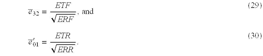
- This decoupling process includes a novel sign ambiguity determination method for calculating and resolving the square root of the forward and reverse reflection tracking terms (ETR, ERR), which are needed to effectively localize the forward and reverse transmission tracking terms (ETF, ERF).
- test port P4 ( 58 ) were connected to Port 1 26 of the VNA, then its local error parameters, e 00 , e 10 , e 01 , e 11 , e′ 1 , and e′ 11 would be independent of which of the other test ports P1-P3 was connected to Port 2 ( 28 ) of the analyzer.
- test ports are independent in this sense, then a standard calibration procedure has a great deal of redundancy. It is, in part, by eliminating this redundancy that the number of required test port interconnections can be reduced. It should be noted that no particular assumptions are required for the leakage terms EXF, EXR. These terms are determined by transmission measurements with all test ports disconnected (and usually terminated). The instrument can therefore cycle through all the paths automatically and determine the leakage terms without manual intervention.
- Equations (4-12) reveal an issue with this scheme that requires an additional assumption to reduce the number of full calibration steps to a minimum.
- This issue relates to the fact that the error parameters e 10 , e 32 , and e′ 23 , e′ 01 do not appear individually, but in the combinations ETF (e 10 *e 32 ), and ETR (e′ 23 *e′ 01 ) which are referred to as “the transmission tracking terms.” Indeed, no measurement on calibration standards alone can determine these error parameters in isolation.
- ⁇ overscore (e) ⁇ 32 and ⁇ overscore (e) ⁇ ′ 01 are identical to e 32 and e′ 01 , except that the ⁇ terms are missing. Since these terms cancel out in the final equations (see equations 31 and 32, below), it is only necessary to determine the ratios defined by ⁇ overscore (e) ⁇ 32 and ⁇ overscore (e) ⁇ ′ 01 in order to properly construct the non-calibrated test paths.
- This preferred calibration procedure only requires that the test ports (P1-P4) be calibrated in pairs in such a way that each test port is included in at least one pair.
- the interconnection scheme could therefore be (P1, P2), (P3, P4) for the hypothetical four-port test system shown in FIG. 1, although any other physically convenient pairing could be used.
- a full 12-term calibration procedure is performed.
- calibration measurements are made with the ports of the network analyzer (Port 1, Port 2) connected to the test ports (P1-P4) in both possible senses.
- reflection measurements are made of each test port in its terminated state.
- the total number of operations performed by the test technician is exactly the same as for a conventional 12-term calibration, but in this case the analyzer performs considerably more measurements on each calibration component.
- the error terms for paths 1 and 3 are then known from the actual measurements on these test ports.
- each test port in any path can be treated independently of the others.
- the error terms for the remaining paths (2, 4, 5 and 6) can be constructed from the localized error parameters for the two ports in the respective path. This procedure is described in more detail below.
- FIGS. 4-6 describe in more detail the method steps carried out by an S parameter measurement system programmed to function according to the present invention.
- FIG. 4 is a flowchart of a preferred series of steps for calibrating an n-port S parameter measurement system such as shown in FIG. 1 .
- FIG. 5 is a flowchart of a preferred series of steps for decoupling the forward and reverse error tracking terms in the 12-term error model.
- FIG. 6 is a plot showing the zero-frequency phase extrapolation step utilized to resolve the sign ambiguity in the square root calculation of the forward and reverse reflection tracking terms.
- the preferred method discussed herein is applicable to any RF measurements made using a VNA (or other equivalent device) for characterizing the S parameters of a DUT.
- VNA or other equivalent device
- the invention is capable of many distinct implementations. It can be implemented as a method of operation. It can be implemented as a system or apparatus including computer software (or firmware) programming for executing the preferred method of operation. It can be implemented as an article of manufacture (i.e., a series of computer-implemented steps stored on a magnetic medium, such as a floppy disk, CD-ROM or other transportable storage device.) These are just some of the many implementations that the present invention may take.
- each path is characterized by two twelve-term error models, which are chosen for each of the two possible ways of connecting the chosen test ports (P1-P4) to the VNA 10 .
- Table 1.0 set forth below.
- the measurements for a given pair of test ports are performed automatically, both senses can be calibrated in one operation and thus, only six pairs of ports need to be connected in order to fully calibrate the system.
- n(n ⁇ 1)/2 such pairings are required.
- This methodology is preferably implemented as software instructions stored in the memory 14 of the VNA 10 .
- These software instructions can be installed into the VNA memory via a floppy disk or other transportable medium, or they may be permanently installed in the VNA memory, such as in a ROM, Flash ROM, EEPROM, or other type of memory device.
- the first step of the method 80 is to select the desired n/2 test port pairings.
- Each test port must participate in at least one pairing.
- a standard full calibration is conducted on the pairings 82 .
- This full calibration step can be done according to several well-established and published techniques, such as SOLT (Short Open Load Through), LRM (Line Reflect Match) or TRL (Through Reflect Line), or can be done using any other suitable combination of calibration components.
- SOLT Short Open Load Through
- LRM Line Reflect Match
- TRL Through Reflect Line
- each method relies upon measuring certain calibration components in order to solve the error contributions in the standard 12-term model (or whatever other model is being used).
- 12 independent measurements at the test ports must be made.
- a typical procedure involves reflection measurements on three known impedance standards at each of the two test ports (6 measurements), transmission and reflection measurements on a through connection with known properties (4 measurements), and transmission measurements with the test ports disconnected and terminated with matched loads (2 measurements).
- the measured S parameters are stored at step 84 .
- This data can be stored in the memory 14 of the VNA 10 , or it could be transferred to a PC or workstation that is controlling the calibration system.
- the full calibration process continues ( 86 , 82 ) until each of the selected n/2 test port pairs is calibrated and the respective S parameters are stored 86 .
- Control of the calibration system then passes to step 90 , in which the measured S parameters gathered during the calibration process ( 82 ) are used to calculate the error terms (EDF, ESF, ELF, EXF, ERF, ETF, EDR, ESR, ELR, EXR, ERR, and ETR) associated with each test port pair.
- error terms EDF, ESF, ELF, EXF, ERF, ETF, EDR, ESR, ELR, EXR, ERR, and ETR
- control of the calibration system passes to step 92 , in which the error terms associated with the test port pairings are decoupled into error parameters that are localized to the individual test port to which they are associated by virtue of the independence assumption. These local error parameters are then stored per test port for use in constructing the error model for the non-measured paths.
- the error terms are decoupled from the port pair into localized error parameters associated with just one of the test ports.
- the first way relates to the transmission tracking terms (ETF, ETR), and is more thoroughly described below in connections with FIGS. 5 and 6.
- the second way (which is less complex than the first) relates to the remaining error terms. These terms are decoupled from the port pairing by disassociating the term from the port path that is calibrated and by associating the error parameters that comprise the term with one of the respective test ports that form the path.
- the error terms EDF, ESF, ERF, ELF, EDR, ESR, ERR and ELR can be decoupled from the test path (path 1) into the local error parameters e 00 , e 11 , e 10 *e 01 , e 22 , e′ 33 , e′ 22 , e′ 23 *e′ 32 and e′ 11 by disassociating these terms from the test port pairing (path 1), and associating the local parameters with the individual test ports (P1 or P2).
- FIG. 5 a flowchart is set forth showing a preferred series of steps for decoupling the forward and reverse error tracking terms into local error parameters.
- the parameters ⁇ overscore (e) ⁇ 32 and ⁇ overscore (e) ⁇ ′ 01 are identical to e 32 and e′ 01 , except that the ⁇ terms are missing. However, as shown in equations 31 and 32, these terms cancel out, and thus it is only necessary to determine the ratios defined by ⁇ overscore (e) ⁇ 32 and ⁇ overscore (e) ⁇ ′ 01 in order to properly construct the non-calibrated test paths.
- step 106 the complex square root of the ERF and ERR terms is calculated using data from step 108 to resolve the sign ambiguity of these square root terms (step 108 is described in more detail below.)
- Equations (31) and (32) thus express ETF and ETR as products of error parameters which can be explicitly determined and are localized to a particular test port.
- FIG. 6 is a plot showing the zero-frequency phase extrapolation step.
- the X-axis of the plot 124 shows frequency in Hz, and the Y-axis shows phase, measured in degrees.
- the data plots 126 , 128 show the ERF (or ERR) data for two test ports (as solid lines), and the extrapolated data as dashed lines.
- the absolute phase of ERF or ERR can be extracted.
- the square root can be taken using the following expression in complex polar notation:
- R the modulus or magnitude of the complex number
- 0 the argument or phase of the complex number
- test port pairing P1-P2 connected to ports 1 and 2 of the analyzer, respectively
- error parameter ⁇ overscore (e) ⁇ ′ 01 would be localized to test port P1 (since it is connected to Port 1 of the VNA), and parameter ⁇ overscore (e) ⁇ 32 would be associated with test port P2.
- step 98 the error model for each of the non-measured paths is constructed using the error parameters stored in step 94 for the individual test ports. For example, using the calibration data from path 1 (P1-P2) and path 3 (P4-P3), the error model for path 5 (P1-P3) can be constructed as shown in Table 3.0.
- the isolation terms (EXF, EXR) between test ports can be ignored in most applications. If the isolation terms are required, then they are measured with the test ports disconnected, so no additional calibration is needed.
- step 96 the error model terms for the non-measured paths are constructed.
- step 100 control of the system passes to step 100 , where a DUT 50 is attached to the system for actual S parameter measurements.
- these measured S parameters (S M ) for the DUT 50 can be corrected to give the actual S parameters (S A ) by solving the standard equations given above (4-12) using the error data stored at steps 88 and 96 .
- the actual S parameters of any n-port DUT can be accurately determined using a calibration methodology that requires only n/2 full calibration measurements for the VNA test setup.
- This preferred methodology provides many advantages over presently known calibration methods for measuring the S parameters of a multi-port DUT. Foremost among these many advantages is that it allows full calibration of an n-port test system with at most n/2 interconnections between test ports. This, in turn, permits true n-port error correction.
- n/2 calibration methodology reduces the number of full calibrations even further if a four-sampler VNA is used. With such a setup, it is possible to calibrate the system so that only one full two-port calibration is needed, and n ⁇ 2 reflection calibrations.
- the DUT 50 shown in FIG. 1 is assigned three arbitrary interface types as defined in Table 4.0 below.
- the VNA system can be calibrated by performing a full two-port calibration between test ports P2-P4 and two reflection calibrations, one on test port P1 using 3.5 mm calibration standards and one on test port P3 using TNC calibration standards.
- the full twelve-term error models can then be constructed from the error terms gathered during the calibration of the system.
- test ports P1 and P3 ( 52 , 56 ) are calibrated using a single reflection calibration
- test ports P2-P4 (Path 6) are calibrated using a full two-port calibration.
- the error parameters for each of the ports are determined by decoupling and localizing the parameters so that each port can be treated independently from the others.
- the error terms for path P1-P3 can be constructed using the measured error parameters from the partial calibrations of ports 1 and 3, and the full calibration of path P2-P4.
- the four remaining combinations of test ports P1-P2, P1-P4, P2-P3 and P3-P4 can be constructed.
- K f and K r are calculated based on error parameters from P2-P4 they are, in fact, independent of the test ports they are measured from and can be applied universally to all of the other test ports. In this manner an n-port system can be calibrated using one full two-port calibration and n ⁇ 2 reflection calibrations, which is again a significant reduction from the n/2 case.
Abstract
Description


| TABLE 1.0 |
| Conventional Calibration Path Connectivity for a Four-Port Device |
| Test Ports | Switch to |
Switch to |
| P1-P2 | P1 | P2 |
| P2-P1 | P2 | P1 |
| P1-P3 | P1 | P3 |
| P3-P1 | P3 | P1 |
| P1-P4 | P1 | P4 |
| P4-P1 | P4 | P1 |
| P2-P3 | P2 | P3 |
| P3-P2 | P3 | P2 |
| P2-P4 | P2 | P4 |
| P4-P2 | P4 | P2 |
| P3-P4 | P3 | P4 |
| P4-P3 | P4 | P3 |
| TABLE 2.0 |
| N/2 Calibration Path Connectivity for a Four Port Device |
| Test Ports | Switch to |
Switch to |
| P1-P2 | P1 | P2 |
| P2-P1 | P2 | P1 |
| P3-P4 | P3 | P4 |
| P4-P3 | P4 | P3 |


| TABLE 3.0 |
| Summary of Error Term Construction |
| P1-P2 | P4-P3 | P1-P3 | ||
| EDF(P1-P2) | EDF(P4-P3) | EDF(P1-P3) = e00(P1) | ||
| ERF(P1-P2) | ERF(P4-P3) | ERF(P1-P3) = e10(P1) * e01(P1) | ||
| ESF(P1-P2) | ESF(P4-P3) | ESF(P1-P3) = e11(P1) | ||
| ELF(P1-P2) | ELF(P4-P3) | ELF(P1-P3) = e22(P3) | ||
| ETF(P1-P2) | ETF(P4-P3) |
 |
||
| EDR(P1-P2) | EDR(P4-P3) | EDR(P1-P3) = e′33(P3) | ||
| ERR(P1-P2) | ERR(P4-P3) | ERR(P1-P3) = e′23(P3) * e′32(P3) | ||
| ESR(P1-P2) | ESR(P4-P3) | ESR(P1-P3) = e′22(P3) | ||
| ELR(P1-P2) | ELR(P4-P3) | ELR(P1-P3) = e′11(P1) | ||
| ETR(P1-P2) | ETR(P4-P3) |
 |
||
| TABLE 3.1 |
| Summary of Error Term Construction for Complete Data Set |
| Calibration | ||
| Required Path | Data with |
Calibration Data with |
| to Construct | of VNA as a Source | of VNA as a Receiver |
| P1-P3 | P1-P2 | P4-P3 |
| P3-P1 | P3-P4 | P2-P1 |
| P1-P4 | P1-P2 | P3-P4 |
| P4-P1 | P4-P3 | P2-P1 |
| P2-P3 | P2-P1 | P4-P3 |
| P3-P2 | P3-P4 | P1-P2 |
| P2-P4 | P2-P1 | P3-P4 |
| P4-P2 | P4-P3 | P1-P2 |
| TABLE 4.0 |
| DUT Connector Configuration and Type |
| DUT Port | Connector Type |
| J1 | 3.5 mm |
| J2 | Waveguide |
| J3 | TNC |
| J4 | Waveguide - Same size as J2 |
| TABLE 4.1 |
| Example of Error Term Construction for P1-P3 |
| |
|
||
| Source | Source | Path P2-P4 | P1-P3 Constructed Error Terms |
| P1 | P3 | P2-P4 | P1-P3 |
| EDF(P1) | EDF(P3) | EDF(P2-P4) | EDF(P1-P3) = e00(P1) |
| ERF(P1) | ERF(P3) | ERF(P2-P4) | ERF(P1-P3) = e10(P1) * e01(P1) |
| ESF(P1) | ESF(P3) | ESF(P2-P4) | ESF(P1-P3) = e11(P1) |
| ELF(P2-P4) | ELF(P1-P3) = e′22(P3) | ||
| ETF(P2-P4) |
 |
||
| EDR(P2-P4) | EDR(P1-P3) = e′33(P3) | ||
| ERR(P2-P4) | ERR(P1-P3) = e′23(P3) * e′32(P3) | ||
| ESR(P2-P4) | ESR(P1-P3) = e′22(P3) | ||
| ELR(P2-P4) | ELR(P1-P3) = e11(P1) | ||
| ETR(P2-P4) |
 |
||

Claims (31)


Priority Applications (5)
| Application Number | Priority Date | Filing Date | Title |
|---|---|---|---|
| US09/241,704 US6300775B1 (en) | 1999-02-02 | 1999-02-02 | Scattering parameter calibration system and method |
| PCT/CA2000/000087 WO2000046605A2 (en) | 1999-02-02 | 2000-02-01 | Scattering parameter calibration system and method |
| EP00901456A EP1181562B8 (en) | 1999-02-02 | 2000-02-01 | Scattering parameter calibration system and method |
| DE60034121T DE60034121T2 (en) | 1999-02-02 | 2000-02-01 | METHOD AND DEVICE FOR STREUPARAMETER CALIBRATION |
| CA002361666A CA2361666C (en) | 1999-02-02 | 2000-02-01 | Scattering parameter calibration system and method |
Applications Claiming Priority (1)
| Application Number | Priority Date | Filing Date | Title |
|---|---|---|---|
| US09/241,704 US6300775B1 (en) | 1999-02-02 | 1999-02-02 | Scattering parameter calibration system and method |
Publications (1)
| Publication Number | Publication Date |
|---|---|
| US6300775B1 true US6300775B1 (en) | 2001-10-09 |
Family
ID=22911826
Family Applications (1)
| Application Number | Title | Priority Date | Filing Date |
|---|---|---|---|
| US09/241,704 Expired - Lifetime US6300775B1 (en) | 1999-02-02 | 1999-02-02 | Scattering parameter calibration system and method |
Country Status (5)
| Country | Link |
|---|---|
| US (1) | US6300775B1 (en) |
| EP (1) | EP1181562B8 (en) |
| CA (1) | CA2361666C (en) |
| DE (1) | DE60034121T2 (en) |
| WO (1) | WO2000046605A2 (en) |
Cited By (65)
| Publication number | Priority date | Publication date | Assignee | Title |
|---|---|---|---|---|
| US6571187B1 (en) * | 2000-02-09 | 2003-05-27 | Avaya Technology Corp. | Method for calibrating two port high frequency measurements |
| US20030115008A1 (en) * | 2001-12-18 | 2003-06-19 | Yutaka Doi | Test fixture with adjustable pitch for network measurement |
| US6614237B2 (en) * | 2000-09-18 | 2003-09-02 | Agilent Technologies, Inc. | Multiport automatic calibration device for a multiport test system |
| US20030173975A1 (en) * | 2002-03-14 | 2003-09-18 | Adamian Vahe?Apos; A. | Method, apparatus, and article of manufacture for characterizing a device and predicting electrical behavior of the device in a circuit |
| US6643597B1 (en) * | 2001-08-24 | 2003-11-04 | Agilent Technologies, Inc. | Calibrating a test system using unknown standards |
| US6647357B1 (en) * | 2000-02-07 | 2003-11-11 | Avaya Technology Corp. | Method for correcting reciprocity error in two port network measurements |
| US6650123B2 (en) * | 2002-01-15 | 2003-11-18 | Anritsu Company | Methods for determining characteristics of interface devices used with vector network analyzers |
| US20040095145A1 (en) * | 2002-11-14 | 2004-05-20 | Ali Boudiaf | Method and apparatus for performing multiport through-reflect-line calibration and measurement |
| US20040100276A1 (en) * | 2002-11-25 | 2004-05-27 | Myron Fanton | Method and apparatus for calibration of a vector network analyzer |
| US20040153265A1 (en) * | 2003-01-30 | 2004-08-05 | Anritsu Company | Flexible vector network analyzer measurements and calibrations |
| US20040174172A1 (en) * | 2003-03-05 | 2004-09-09 | Gaku Kamitani | Method of correcting measurement error and electronic component characteristic measurement apparatus |
| US20040193382A1 (en) * | 2000-09-18 | 2004-09-30 | Adamian Vahe' A. | Method and apparatus for calibrating a multiport test system for measurement of a DUT |
| US20040251922A1 (en) * | 2003-06-12 | 2004-12-16 | Anritsu Company | Methods and computer program products for full N-port vector network analyzer calibrations |
| US20040257092A1 (en) * | 2003-06-11 | 2004-12-23 | Jan Verspecht | Method and a test setup for measuring large-signal S-parameters |
| US6836743B1 (en) * | 2002-10-15 | 2004-12-28 | Agilent Technologies, Inc. | Compensating for unequal load and source match in vector network analyzer calibration |
| EP1490910A2 (en) * | 2002-03-29 | 2004-12-29 | Agilent Technologies | Determination apparatus and method of calibrating the apparatus |
| US20050030047A1 (en) * | 2003-08-05 | 2005-02-10 | Vahe Adamian | Method and apparatus for measuring a device under test using an improved through-reflect-line measurement calibration |
| US20050093554A1 (en) * | 2003-11-05 | 2005-05-05 | Yong Wang | System and method for determining S-parameters using a load |
| US20050110502A1 (en) * | 2003-11-05 | 2005-05-26 | Yong Wang | System and method for determining S-parameters |
| US20050200365A1 (en) * | 2002-09-16 | 2005-09-15 | Anritsu Company | Apparatus for use in calibrating a VNA |
| US6965241B1 (en) * | 2003-10-07 | 2005-11-15 | Agilent Technologies, Inc. | Automated electronic calibration apparatus |
| US20050256658A1 (en) * | 2004-05-12 | 2005-11-17 | Anderson Keith F | Multi-port scattering parameter calibration system and method |
| US6995571B1 (en) * | 2005-01-03 | 2006-02-07 | Agilent Technologies, Inc. | Vector network analyzer mixer calibration using the unknown thru calibration |
| US20060055394A1 (en) * | 2004-09-13 | 2006-03-16 | Joel Dunsmore | Network analyzer including automatic port extension calibration and method of operation |
| US7030625B1 (en) | 2005-01-18 | 2006-04-18 | Agilent Technologies, Inc. | Method and apparatus for performing a minimum connection multiport through-reflect-line calibration and measurement |
| US20060084426A1 (en) * | 2004-10-18 | 2006-04-20 | Anderson Keith F | Vector network analyzer with independently tuned receivers characterizes frequency translation devices |
| GB2421802A (en) * | 2005-01-03 | 2006-07-05 | Agilent Technologies Inc | Two-tier vector network analyser calibration process |
| GB2421803A (en) * | 2005-01-03 | 2006-07-05 | Agilent Technologies Inc | Multi-port vector neywork analyzer calibration using the "unknown thru" method |
| US20060155498A1 (en) * | 2003-06-11 | 2006-07-13 | Dunsmore Joel P | Correcting test system calibration and transforming device measurements when using multiple test fixtures |
| US20060226856A1 (en) * | 2005-03-30 | 2006-10-12 | Wong Kenneth H | VNA and method for addressing transmission line effects in VNA measurement data |
| GB2426089A (en) * | 2005-05-12 | 2006-11-15 | Agilent Technologies Inc | Topology-independent calibration system and method of determining path errors in a test system |
| US7138813B2 (en) | 1999-06-30 | 2006-11-21 | Cascade Microtech, Inc. | Probe station thermal chuck with shielding for capacitive current |
| US7231308B2 (en) * | 2001-12-21 | 2007-06-12 | Agilent Technologies, Inc. | Test system dynamic range extension through compression compensation |
| US7355420B2 (en) | 2001-08-21 | 2008-04-08 | Cascade Microtech, Inc. | Membrane probing system |
| US7359814B1 (en) | 2000-02-07 | 2008-04-15 | Advantest | Multi-port analysis apparatus and method and calibration method thereof |
| US7420381B2 (en) | 2004-09-13 | 2008-09-02 | Cascade Microtech, Inc. | Double sided probing structures |
| US20080258738A1 (en) * | 2007-04-20 | 2008-10-23 | Anritsu Company | Characterizing test fixtures |
| US7492172B2 (en) | 2003-05-23 | 2009-02-17 | Cascade Microtech, Inc. | Chuck for holding a device under test |
| EP2081031A1 (en) | 2008-01-17 | 2009-07-22 | Com Dev International Limited | Method and system for tracking scattering parameter test system calibration |
| US20090234610A1 (en) * | 2008-03-13 | 2009-09-17 | Spinner Gmbh | Arrangement for Calibrating a Vector Network Analyzer |
| US20090319217A1 (en) * | 2006-07-03 | 2009-12-24 | Rosenberger Hochfrequenztechnik Gmbh & Co. Kg | Hf measurement system, method for the calibration thereof, and method for determining scattering parameters with this hf measurement system |
| US7656172B2 (en) | 2005-01-31 | 2010-02-02 | Cascade Microtech, Inc. | System for testing semiconductors |
| US7681312B2 (en) | 1998-07-14 | 2010-03-23 | Cascade Microtech, Inc. | Membrane probing system |
| US7688062B2 (en) | 2000-09-05 | 2010-03-30 | Cascade Microtech, Inc. | Probe station |
| US7688097B2 (en) | 2000-12-04 | 2010-03-30 | Cascade Microtech, Inc. | Wafer probe |
| US7688091B2 (en) | 2003-12-24 | 2010-03-30 | Cascade Microtech, Inc. | Chuck with integrated wafer support |
| US7723999B2 (en) | 2006-06-12 | 2010-05-25 | Cascade Microtech, Inc. | Calibration structures for differential signal probing |
| US20100161265A1 (en) * | 2008-12-19 | 2010-06-24 | Rohde & Schwarz Gmbh & Co. Kg | 9-term calibration method for network analyzers |
| US7750652B2 (en) | 2006-06-12 | 2010-07-06 | Cascade Microtech, Inc. | Test structure and probe for differential signals |
| US7759953B2 (en) | 2003-12-24 | 2010-07-20 | Cascade Microtech, Inc. | Active wafer probe |
| US7764072B2 (en) | 2006-06-12 | 2010-07-27 | Cascade Microtech, Inc. | Differential signal probing system |
| US7876114B2 (en) | 2007-08-08 | 2011-01-25 | Cascade Microtech, Inc. | Differential waveguide probe |
| US7888957B2 (en) | 2008-10-06 | 2011-02-15 | Cascade Microtech, Inc. | Probing apparatus with impedance optimized interface |
| US7893704B2 (en) | 1996-08-08 | 2011-02-22 | Cascade Microtech, Inc. | Membrane probing structure with laterally scrubbing contacts |
| US7898273B2 (en) | 2003-05-23 | 2011-03-01 | Cascade Microtech, Inc. | Probe for testing a device under test |
| US7898281B2 (en) | 2005-01-31 | 2011-03-01 | Cascade Mircotech, Inc. | Interface for testing semiconductors |
| US7969173B2 (en) | 2000-09-05 | 2011-06-28 | Cascade Microtech, Inc. | Chuck for holding a device under test |
| US8069491B2 (en) | 2003-10-22 | 2011-11-29 | Cascade Microtech, Inc. | Probe testing structure |
| US8319503B2 (en) | 2008-11-24 | 2012-11-27 | Cascade Microtech, Inc. | Test apparatus for measuring a characteristic of a device under test |
| CN102841261A (en) * | 2011-06-22 | 2012-12-26 | 纬创资通股份有限公司 | Method for measuring scattering parameter of object to be measured |
| US8410806B2 (en) | 2008-11-21 | 2013-04-02 | Cascade Microtech, Inc. | Replaceable coupon for a probing apparatus |
| US20160178722A1 (en) * | 2014-12-22 | 2016-06-23 | Fraunhofer-Gesellschaft Zur Forderung Der Angewandten Forschung E.V. | Method for characterizing microwave components |
| CN107390052A (en) * | 2017-07-03 | 2017-11-24 | 北京理工雷科电子信息技术有限公司 | A kind of Feature Analyzes method based on multiport ABCD parameters |
| US10396907B2 (en) * | 2010-02-01 | 2019-08-27 | Teledyne Lecroy, Inc. | Time domain reflectometry step to S-parameter conversion |
| US11428770B2 (en) * | 2020-03-30 | 2022-08-30 | Rohde & Schwarz Gmbh & Co. Kg | Method of calibrating a setup |
Families Citing this family (7)
| Publication number | Priority date | Publication date | Assignee | Title |
|---|---|---|---|---|
| US7061254B1 (en) * | 2005-05-12 | 2006-06-13 | Agilent Technologies, Inc. | Power calibration for multi-port vector network analyzer (VNA) |
| US7924025B2 (en) * | 2005-07-25 | 2011-04-12 | University Of Florida Research Foundation, Inc. | System, device, and method for embedded S-parameter measurement |
| DE102012006314A1 (en) * | 2012-03-28 | 2013-10-02 | Rosenberger Hochfrequenztechnik Gmbh & Co. Kg | Time domain measurement with calibration in the frequency domain |
| US11041894B2 (en) * | 2017-08-18 | 2021-06-22 | Rohde & Schwarz Gmbh & Co. Kg | Vector network analyzer with digital interface |
| CN111257814A (en) * | 2020-03-05 | 2020-06-09 | 西北工业大学 | Straight-through-short circuit calibration method of vector network analyzer |
| EP3951405A1 (en) * | 2020-08-07 | 2022-02-09 | Rohde & Schwarz GmbH & Co. KG | Measurement system and measurement method |
| CN112051534B (en) * | 2020-08-31 | 2023-08-25 | 中电科思仪科技股份有限公司 | External device and method for improving measurement and calibration precision of microwave network |
Citations (17)
| Publication number | Priority date | Publication date | Assignee | Title |
|---|---|---|---|---|
| US4816767A (en) * | 1984-01-09 | 1989-03-28 | Hewlett-Packard Company | Vector network analyzer with integral processor |
| US4853613A (en) | 1987-10-27 | 1989-08-01 | Martin Marietta Corporation | Calibration method for apparatus evaluating microwave/millimeter wave circuits |
| US4982164A (en) | 1988-04-22 | 1991-01-01 | Rhode & Schwarz Gmbh & Co. K.G. | Method of calibrating a network analyzer |
| US5313166A (en) | 1990-11-11 | 1994-05-17 | Rohde & Schwarz Gmbh & Co. Kg | Method of calibrating a network analyzer |
| US5434511A (en) | 1993-05-24 | 1995-07-18 | Atn Microwave, Inc. | Electronic microwave calibration device |
| US5440236A (en) | 1992-05-02 | 1995-08-08 | Rohde & Schwarz Gmbh & Co. Kg | Calibrating a network analyzer by making multiple measurements on a common transmission line with a movable discontinuity |
| US5442296A (en) | 1992-12-12 | 1995-08-15 | Rohde & Schwarz Gmbh & Co. Kg | Method for calibrating a network analyzer |
| US5467021A (en) | 1993-05-24 | 1995-11-14 | Atn Microwave, Inc. | Calibration method and apparatus |
| GB2292616A (en) | 1994-08-24 | 1996-02-28 | Hewlett Packard Co | Calibration of a circuit network measurement device |
| US5587934A (en) | 1993-10-21 | 1996-12-24 | Wiltron Company | Automatic VNA calibration apparatus |
| US5608330A (en) | 1994-10-05 | 1997-03-04 | Rohde & Schwarz Gmbh & Co. Kg | Method for calibrating a network analyzer according to the seven-term principle |
| US5661404A (en) | 1994-07-27 | 1997-08-26 | Hewlett-Packard Company | Circuit network measurement device and calibration method |
| US5748506A (en) | 1996-05-28 | 1998-05-05 | Motorola, Inc. | Calibration technique for a network analyzer |
| US5751153A (en) | 1994-07-05 | 1998-05-12 | Motorola, Inc. | Method and apparatus for characterizing a multiport circuit |
| US5784299A (en) | 1996-02-24 | 1998-07-21 | Rohde & Schwarz Gmbh & Co. Kg | Method for measuring electronic devices under test with a network analyzer |
| US5793213A (en) | 1996-08-01 | 1998-08-11 | Motorola, Inc. | Method and apparatus for calibrating a network analyzer |
| DE19828682A1 (en) | 1997-08-26 | 1999-03-18 | Hewlett Packard Co | Automatic calibration of a network analyzer |
-
1999
- 1999-02-02 US US09/241,704 patent/US6300775B1/en not_active Expired - Lifetime
-
2000
- 2000-02-01 CA CA002361666A patent/CA2361666C/en not_active Expired - Fee Related
- 2000-02-01 DE DE60034121T patent/DE60034121T2/en not_active Expired - Lifetime
- 2000-02-01 EP EP00901456A patent/EP1181562B8/en not_active Expired - Lifetime
- 2000-02-01 WO PCT/CA2000/000087 patent/WO2000046605A2/en active IP Right Grant
Patent Citations (23)
| Publication number | Priority date | Publication date | Assignee | Title |
|---|---|---|---|---|
| US4816767A (en) * | 1984-01-09 | 1989-03-28 | Hewlett-Packard Company | Vector network analyzer with integral processor |
| US4853613A (en) | 1987-10-27 | 1989-08-01 | Martin Marietta Corporation | Calibration method for apparatus evaluating microwave/millimeter wave circuits |
| US4982164A (en) | 1988-04-22 | 1991-01-01 | Rhode & Schwarz Gmbh & Co. K.G. | Method of calibrating a network analyzer |
| US5313166A (en) | 1990-11-11 | 1994-05-17 | Rohde & Schwarz Gmbh & Co. Kg | Method of calibrating a network analyzer |
| US5440236A (en) | 1992-05-02 | 1995-08-08 | Rohde & Schwarz Gmbh & Co. Kg | Calibrating a network analyzer by making multiple measurements on a common transmission line with a movable discontinuity |
| US5442296A (en) | 1992-12-12 | 1995-08-15 | Rohde & Schwarz Gmbh & Co. Kg | Method for calibrating a network analyzer |
| US5548221A (en) | 1993-05-24 | 1996-08-20 | Atn Microwave, Inc. | Electronic calibration method and apparatus |
| US5467021A (en) | 1993-05-24 | 1995-11-14 | Atn Microwave, Inc. | Calibration method and apparatus |
| US5537046A (en) | 1993-05-24 | 1996-07-16 | Atn Microwave, Inc. | Electronic calibration method and apparatus |
| US5434511A (en) | 1993-05-24 | 1995-07-18 | Atn Microwave, Inc. | Electronic microwave calibration device |
| US5552714A (en) | 1993-05-24 | 1996-09-03 | Atn Microwave, Inc. | Electronic calibration method and apparatus |
| US5578932A (en) | 1993-05-24 | 1996-11-26 | Atn Microwave, Inc. | Method and apparatus for providing and calibrating a multiport network analyzer |
| US5587934A (en) | 1993-10-21 | 1996-12-24 | Wiltron Company | Automatic VNA calibration apparatus |
| US5751153A (en) | 1994-07-05 | 1998-05-12 | Motorola, Inc. | Method and apparatus for characterizing a multiport circuit |
| US5661404A (en) | 1994-07-27 | 1997-08-26 | Hewlett-Packard Company | Circuit network measurement device and calibration method |
| US5646536A (en) | 1994-08-24 | 1997-07-08 | Hewlett-Packard Company | Method for calibrating circuit network measurement devices |
| GB2292616A (en) | 1994-08-24 | 1996-02-28 | Hewlett Packard Co | Calibration of a circuit network measurement device |
| US5608330A (en) | 1994-10-05 | 1997-03-04 | Rohde & Schwarz Gmbh & Co. Kg | Method for calibrating a network analyzer according to the seven-term principle |
| US5666059A (en) | 1994-10-05 | 1997-09-09 | Rohde & Schwarz Gmbh & Co. Kg | Method for calibrating a network analyzer according to the fifteen-term principle |
| US5784299A (en) | 1996-02-24 | 1998-07-21 | Rohde & Schwarz Gmbh & Co. Kg | Method for measuring electronic devices under test with a network analyzer |
| US5748506A (en) | 1996-05-28 | 1998-05-05 | Motorola, Inc. | Calibration technique for a network analyzer |
| US5793213A (en) | 1996-08-01 | 1998-08-11 | Motorola, Inc. | Method and apparatus for calibrating a network analyzer |
| DE19828682A1 (en) | 1997-08-26 | 1999-03-18 | Hewlett Packard Co | Automatic calibration of a network analyzer |
Non-Patent Citations (4)
| Title |
|---|
| "An Automatic Network Analyzer System"; Hackborn, R.A.; Microwave Journal, pp. 45-52, May 1968. |
| "Error Models For Systems Measurement"; Fitzpatrick, J.; Microwave Journal, pp. 63-66, May 1978. |
| "Network Analyzer Basics"; Ballo, David; Hewlett-Packard Company, 1998 Back to Basics Seminar (1997). No month available. |
| Ferrero A. et al., "A New Implementation Of A Multiport Automatic Network Analyzer", IEEE Transactions On Microwave Theory And Techniques, US, IEE Inc., New York, vol. 40, No. 11, Nov. 1, 1992, pp. 2078-2085. |
Cited By (110)
| Publication number | Priority date | Publication date | Assignee | Title |
|---|---|---|---|---|
| US7893704B2 (en) | 1996-08-08 | 2011-02-22 | Cascade Microtech, Inc. | Membrane probing structure with laterally scrubbing contacts |
| US8451017B2 (en) | 1998-07-14 | 2013-05-28 | Cascade Microtech, Inc. | Membrane probing method using improved contact |
| US7681312B2 (en) | 1998-07-14 | 2010-03-23 | Cascade Microtech, Inc. | Membrane probing system |
| US7761986B2 (en) | 1998-07-14 | 2010-07-27 | Cascade Microtech, Inc. | Membrane probing method using improved contact |
| US7138813B2 (en) | 1999-06-30 | 2006-11-21 | Cascade Microtech, Inc. | Probe station thermal chuck with shielding for capacitive current |
| US7359814B1 (en) | 2000-02-07 | 2008-04-15 | Advantest | Multi-port analysis apparatus and method and calibration method thereof |
| US6647357B1 (en) * | 2000-02-07 | 2003-11-11 | Avaya Technology Corp. | Method for correcting reciprocity error in two port network measurements |
| US6571187B1 (en) * | 2000-02-09 | 2003-05-27 | Avaya Technology Corp. | Method for calibrating two port high frequency measurements |
| US7688062B2 (en) | 2000-09-05 | 2010-03-30 | Cascade Microtech, Inc. | Probe station |
| US7969173B2 (en) | 2000-09-05 | 2011-06-28 | Cascade Microtech, Inc. | Chuck for holding a device under test |
| US20040193382A1 (en) * | 2000-09-18 | 2004-09-30 | Adamian Vahe' A. | Method and apparatus for calibrating a multiport test system for measurement of a DUT |
| US6614237B2 (en) * | 2000-09-18 | 2003-09-02 | Agilent Technologies, Inc. | Multiport automatic calibration device for a multiport test system |
| US20030173978A1 (en) * | 2000-09-18 | 2003-09-18 | Adamian Vahe?Apos; A. | Method and apparatus for calibrating a multiport test system for measurement of a dut |
| US6920407B2 (en) | 2000-09-18 | 2005-07-19 | Agilent Technologies, Inc. | Method and apparatus for calibrating a multiport test system for measurement of a DUT |
| US6826506B2 (en) * | 2000-09-18 | 2004-11-30 | Agilent Technologies, Inc. | Method and apparatus for calibrating a multiport test system for measurement of a DUT |
| US7761983B2 (en) | 2000-12-04 | 2010-07-27 | Cascade Microtech, Inc. | Method of assembling a wafer probe |
| US7688097B2 (en) | 2000-12-04 | 2010-03-30 | Cascade Microtech, Inc. | Wafer probe |
| US7492175B2 (en) | 2001-08-21 | 2009-02-17 | Cascade Microtech, Inc. | Membrane probing system |
| US7355420B2 (en) | 2001-08-21 | 2008-04-08 | Cascade Microtech, Inc. | Membrane probing system |
| US6643597B1 (en) * | 2001-08-24 | 2003-11-04 | Agilent Technologies, Inc. | Calibrating a test system using unknown standards |
| US20030115008A1 (en) * | 2001-12-18 | 2003-06-19 | Yutaka Doi | Test fixture with adjustable pitch for network measurement |
| US7231308B2 (en) * | 2001-12-21 | 2007-06-12 | Agilent Technologies, Inc. | Test system dynamic range extension through compression compensation |
| US6650123B2 (en) * | 2002-01-15 | 2003-11-18 | Anritsu Company | Methods for determining characteristics of interface devices used with vector network analyzers |
| US20040160230A1 (en) * | 2002-03-14 | 2004-08-19 | Adamian Vahe A. | Method, apparatus, and article of manufacture for characterizing a device and predicting electrical behavior of the device in a circuit |
| US20030173975A1 (en) * | 2002-03-14 | 2003-09-18 | Adamian Vahe?Apos; A. | Method, apparatus, and article of manufacture for characterizing a device and predicting electrical behavior of the device in a circuit |
| US6744262B2 (en) * | 2002-03-14 | 2004-06-01 | Agilent Technologies, Inc. | Method, apparatus, and article of manufacture for characterizing a device and predicting electrical behavior of the device in a circuit |
| US6937032B2 (en) | 2002-03-14 | 2005-08-30 | Agilent Technologies, Inc. | Method, apparatus, and article of manufacture for characterizing a device and predicting electrical behavior of the device in a circuit |
| US7184911B2 (en) * | 2002-03-29 | 2007-02-27 | Agilent Technologies, Inc. | Determination apparatus and method of calibrating the apparatus |
| EP1490910A4 (en) * | 2002-03-29 | 2006-10-25 | Agilent Technologies Inc | Determination apparatus and method of calibrating the apparatus |
| US20050165570A1 (en) * | 2002-03-29 | 2005-07-28 | Ryohei Wakai | Determination apparatus and method of calibrating the apparatus |
| EP1490910A2 (en) * | 2002-03-29 | 2004-12-29 | Agilent Technologies | Determination apparatus and method of calibrating the apparatus |
| US7054776B2 (en) * | 2002-09-16 | 2006-05-30 | Anritsu Company | Apparatus for use in calibrating a VNA |
| US20050200365A1 (en) * | 2002-09-16 | 2005-09-15 | Anritsu Company | Apparatus for use in calibrating a VNA |
| US6836743B1 (en) * | 2002-10-15 | 2004-12-28 | Agilent Technologies, Inc. | Compensating for unequal load and source match in vector network analyzer calibration |
| US6853198B2 (en) | 2002-11-14 | 2005-02-08 | Agilent Technologies, Inc. | Method and apparatus for performing multiport through-reflect-line calibration and measurement |
| US20040095145A1 (en) * | 2002-11-14 | 2004-05-20 | Ali Boudiaf | Method and apparatus for performing multiport through-reflect-line calibration and measurement |
| US20040100276A1 (en) * | 2002-11-25 | 2004-05-27 | Myron Fanton | Method and apparatus for calibration of a vector network analyzer |
| US6928373B2 (en) | 2003-01-30 | 2005-08-09 | Anritsu Company | Flexible vector network analyzer measurements and calibrations |
| US20040153265A1 (en) * | 2003-01-30 | 2004-08-05 | Anritsu Company | Flexible vector network analyzer measurements and calibrations |
| US20040183542A1 (en) * | 2003-03-05 | 2004-09-23 | Murata Manufacturing Co., Ltd. | Method for correcting measurement error and electronic component characteristic measurement apparatus |
| US20040174172A1 (en) * | 2003-03-05 | 2004-09-09 | Gaku Kamitani | Method of correcting measurement error and electronic component characteristic measurement apparatus |
| US6960920B2 (en) * | 2003-03-05 | 2005-11-01 | Murata Manufacturing Co., Ltd. | Method for correcting measurement error and electronic component characteristic measurement apparatus |
| US6838885B2 (en) * | 2003-03-05 | 2005-01-04 | Murata Manufacturing Co., Ltd. | Method of correcting measurement error and electronic component characteristic measurement apparatus |
| US7492172B2 (en) | 2003-05-23 | 2009-02-17 | Cascade Microtech, Inc. | Chuck for holding a device under test |
| US7876115B2 (en) | 2003-05-23 | 2011-01-25 | Cascade Microtech, Inc. | Chuck for holding a device under test |
| US7898273B2 (en) | 2003-05-23 | 2011-03-01 | Cascade Microtech, Inc. | Probe for testing a device under test |
| US20060155498A1 (en) * | 2003-06-11 | 2006-07-13 | Dunsmore Joel P | Correcting test system calibration and transforming device measurements when using multiple test fixtures |
| US7500161B2 (en) * | 2003-06-11 | 2009-03-03 | Agilent Technologies, Inc. | Correcting test system calibration and transforming device measurements when using multiple test fixtures |
| US7038468B2 (en) * | 2003-06-11 | 2006-05-02 | Jan Verspecht | Method and a test setup for measuring large-signal S-parameters that include the coefficients relating to the conjugate of the incident waves |
| US20040257092A1 (en) * | 2003-06-11 | 2004-12-23 | Jan Verspecht | Method and a test setup for measuring large-signal S-parameters |
| US20040251922A1 (en) * | 2003-06-12 | 2004-12-16 | Anritsu Company | Methods and computer program products for full N-port vector network analyzer calibrations |
| US6882160B2 (en) | 2003-06-12 | 2005-04-19 | Anritsu Company | Methods and computer program products for full N-port vector network analyzer calibrations |
| US20050030047A1 (en) * | 2003-08-05 | 2005-02-10 | Vahe Adamian | Method and apparatus for measuring a device under test using an improved through-reflect-line measurement calibration |
| US7068049B2 (en) | 2003-08-05 | 2006-06-27 | Agilent Technologies, Inc. | Method and apparatus for measuring a device under test using an improved through-reflect-line measurement calibration |
| US6965241B1 (en) * | 2003-10-07 | 2005-11-15 | Agilent Technologies, Inc. | Automated electronic calibration apparatus |
| US8069491B2 (en) | 2003-10-22 | 2011-11-29 | Cascade Microtech, Inc. | Probe testing structure |
| US6998833B2 (en) * | 2003-11-05 | 2006-02-14 | Hewlett-Packard Development Company, L.P. | System and method for determining S-parameters using a load |
| US20050093554A1 (en) * | 2003-11-05 | 2005-05-05 | Yong Wang | System and method for determining S-parameters using a load |
| US20050110502A1 (en) * | 2003-11-05 | 2005-05-26 | Yong Wang | System and method for determining S-parameters |
| US7688091B2 (en) | 2003-12-24 | 2010-03-30 | Cascade Microtech, Inc. | Chuck with integrated wafer support |
| US7759953B2 (en) | 2003-12-24 | 2010-07-20 | Cascade Microtech, Inc. | Active wafer probe |
| US7113891B2 (en) * | 2004-05-12 | 2006-09-26 | Agilent Technologies, Inc. | Multi-port scattering parameter calibration system and method |
| US20050256658A1 (en) * | 2004-05-12 | 2005-11-17 | Anderson Keith F | Multi-port scattering parameter calibration system and method |
| US7088087B2 (en) * | 2004-09-13 | 2006-08-08 | Agilent Technologies, Inc. | Network analyzer including automatic port extension calibration and method of operation |
| US20060055394A1 (en) * | 2004-09-13 | 2006-03-16 | Joel Dunsmore | Network analyzer including automatic port extension calibration and method of operation |
| US8013623B2 (en) | 2004-09-13 | 2011-09-06 | Cascade Microtech, Inc. | Double sided probing structures |
| US7420381B2 (en) | 2004-09-13 | 2008-09-02 | Cascade Microtech, Inc. | Double sided probing structures |
| US20060084426A1 (en) * | 2004-10-18 | 2006-04-20 | Anderson Keith F | Vector network analyzer with independently tuned receivers characterizes frequency translation devices |
| US7248033B2 (en) * | 2004-10-18 | 2007-07-24 | Agilent Technologies, Inc. | Vector network analyzer with independently tuned receivers characterizes frequency translation devices |
| US7124049B2 (en) | 2005-01-03 | 2006-10-17 | Agilent Technologies, Inc. | Method for implementing TRL calibration in VNA |
| GB2421802B (en) * | 2005-01-03 | 2009-04-15 | Agilent Technologies Inc | Method for Implementing TRL Calibration in VNA |
| GB2421803B (en) * | 2005-01-03 | 2009-04-15 | Agilent Technologies Inc | Multiport Calibration Simplification using the "Unknown Thru" method |
| GB2421802A (en) * | 2005-01-03 | 2006-07-05 | Agilent Technologies Inc | Two-tier vector network analyser calibration process |
| US6995571B1 (en) * | 2005-01-03 | 2006-02-07 | Agilent Technologies, Inc. | Vector network analyzer mixer calibration using the unknown thru calibration |
| US20060161369A1 (en) * | 2005-01-03 | 2006-07-20 | Wong Kenneth H | Method for implementing trl calibration in vna |
| GB2421803A (en) * | 2005-01-03 | 2006-07-05 | Agilent Technologies Inc | Multi-port vector neywork analyzer calibration using the "unknown thru" method |
| US7030625B1 (en) | 2005-01-18 | 2006-04-18 | Agilent Technologies, Inc. | Method and apparatus for performing a minimum connection multiport through-reflect-line calibration and measurement |
| US7656172B2 (en) | 2005-01-31 | 2010-02-02 | Cascade Microtech, Inc. | System for testing semiconductors |
| US7940069B2 (en) | 2005-01-31 | 2011-05-10 | Cascade Microtech, Inc. | System for testing semiconductors |
| US7898281B2 (en) | 2005-01-31 | 2011-03-01 | Cascade Mircotech, Inc. | Interface for testing semiconductors |
| US20060226856A1 (en) * | 2005-03-30 | 2006-10-12 | Wong Kenneth H | VNA and method for addressing transmission line effects in VNA measurement data |
| US7148702B2 (en) * | 2005-03-30 | 2006-12-12 | Agilent Technologies, Inc. | VNA and method for addressing transmission line effects in VNA measurement data |
| GB2426089A (en) * | 2005-05-12 | 2006-11-15 | Agilent Technologies Inc | Topology-independent calibration system and method of determining path errors in a test system |
| US7764072B2 (en) | 2006-06-12 | 2010-07-27 | Cascade Microtech, Inc. | Differential signal probing system |
| US7750652B2 (en) | 2006-06-12 | 2010-07-06 | Cascade Microtech, Inc. | Test structure and probe for differential signals |
| US7723999B2 (en) | 2006-06-12 | 2010-05-25 | Cascade Microtech, Inc. | Calibration structures for differential signal probing |
| US20090319217A1 (en) * | 2006-07-03 | 2009-12-24 | Rosenberger Hochfrequenztechnik Gmbh & Co. Kg | Hf measurement system, method for the calibration thereof, and method for determining scattering parameters with this hf measurement system |
| US8452565B2 (en) * | 2006-07-03 | 2013-05-28 | Rosenberger Hochfrequenztechnik Gmbh & Co. Kg | HF measurement system, method for the calibration thereof, and method for determining scattering parameters with this HF measurement system |
| US20080258738A1 (en) * | 2007-04-20 | 2008-10-23 | Anritsu Company | Characterizing test fixtures |
| US7545151B2 (en) | 2007-04-20 | 2009-06-09 | Anritsu Company | Characterizing test fixtures |
| US7876114B2 (en) | 2007-08-08 | 2011-01-25 | Cascade Microtech, Inc. | Differential waveguide probe |
| US7777497B2 (en) | 2008-01-17 | 2010-08-17 | Com Dev International Ltd. | Method and system for tracking scattering parameter test system calibration |
| EP2081031A1 (en) | 2008-01-17 | 2009-07-22 | Com Dev International Limited | Method and system for tracking scattering parameter test system calibration |
| US20090184721A1 (en) * | 2008-01-17 | 2009-07-23 | Albert-Lebrun Xavier M H | Method and system for tracking scattering parameter test system calibration |
| US8041528B2 (en) * | 2008-03-13 | 2011-10-18 | Spinner Gmbh | Arrangement for calibrating a vector network analyzer |
| US20090234610A1 (en) * | 2008-03-13 | 2009-09-17 | Spinner Gmbh | Arrangement for Calibrating a Vector Network Analyzer |
| US7888957B2 (en) | 2008-10-06 | 2011-02-15 | Cascade Microtech, Inc. | Probing apparatus with impedance optimized interface |
| US8410806B2 (en) | 2008-11-21 | 2013-04-02 | Cascade Microtech, Inc. | Replaceable coupon for a probing apparatus |
| US9429638B2 (en) | 2008-11-21 | 2016-08-30 | Cascade Microtech, Inc. | Method of replacing an existing contact of a wafer probing assembly |
| US10267848B2 (en) | 2008-11-21 | 2019-04-23 | Formfactor Beaverton, Inc. | Method of electrically contacting a bond pad of a device under test with a probe |
| US8319503B2 (en) | 2008-11-24 | 2012-11-27 | Cascade Microtech, Inc. | Test apparatus for measuring a characteristic of a device under test |
| US8340935B2 (en) * | 2008-12-19 | 2012-12-25 | Rohde & Schwarz Gmbh & Co. Kg | 9-term calibration method for network analyzers |
| US20100161265A1 (en) * | 2008-12-19 | 2010-06-24 | Rohde & Schwarz Gmbh & Co. Kg | 9-term calibration method for network analyzers |
| US10396907B2 (en) * | 2010-02-01 | 2019-08-27 | Teledyne Lecroy, Inc. | Time domain reflectometry step to S-parameter conversion |
| CN102841261A (en) * | 2011-06-22 | 2012-12-26 | 纬创资通股份有限公司 | Method for measuring scattering parameter of object to be measured |
| US8860434B2 (en) | 2011-06-22 | 2014-10-14 | Wistron Corp. | Method of measuring scattering parameters of device under test |
| US20160178722A1 (en) * | 2014-12-22 | 2016-06-23 | Fraunhofer-Gesellschaft Zur Forderung Der Angewandten Forschung E.V. | Method for characterizing microwave components |
| CN107390052A (en) * | 2017-07-03 | 2017-11-24 | 北京理工雷科电子信息技术有限公司 | A kind of Feature Analyzes method based on multiport ABCD parameters |
| CN107390052B (en) * | 2017-07-03 | 2019-12-13 | 北京理工雷科电子信息技术有限公司 | System characteristic analysis method based on multiport ABCD parameters |
| US11428770B2 (en) * | 2020-03-30 | 2022-08-30 | Rohde & Schwarz Gmbh & Co. Kg | Method of calibrating a setup |
Also Published As
| Publication number | Publication date |
|---|---|
| EP1181562B8 (en) | 2007-06-27 |
| DE60034121T2 (en) | 2007-11-08 |
| CA2361666C (en) | 2005-11-01 |
| EP1181562A2 (en) | 2002-02-27 |
| WO2000046605A2 (en) | 2000-08-10 |
| DE60034121D1 (en) | 2007-05-10 |
| WO2000046605A3 (en) | 2001-11-29 |
| EP1181562B1 (en) | 2007-03-28 |
| CA2361666A1 (en) | 2000-08-10 |
Similar Documents
| Publication | Publication Date | Title |
|---|---|---|
| US6300775B1 (en) | Scattering parameter calibration system and method | |
| US6882160B2 (en) | Methods and computer program products for full N-port vector network analyzer calibrations | |
| Marks | Formulations of the basic vector network analyzer error model including switch-terms | |
| Hoer | A network analyzer incorporating two six-port reflectometers | |
| US7777497B2 (en) | Method and system for tracking scattering parameter test system calibration | |
| US6650123B2 (en) | Methods for determining characteristics of interface devices used with vector network analyzers | |
| KR100456493B1 (en) | Multi-port device analysis apparatus and method and calibration method thereof | |
| US7068049B2 (en) | Method and apparatus for measuring a device under test using an improved through-reflect-line measurement calibration | |
| US5578932A (en) | Method and apparatus for providing and calibrating a multiport network analyzer | |
| US7235982B1 (en) | Re-calculating S-parameter error terms after modification of a calibrated port | |
| US7061254B1 (en) | Power calibration for multi-port vector network analyzer (VNA) | |
| US8126670B2 (en) | Method and device for calibrating a network analyzer for measuring at differential connections | |
| US6836743B1 (en) | Compensating for unequal load and source match in vector network analyzer calibration | |
| CN104515907B (en) | A kind of scattering parameter test system and its implementation | |
| KR20160048112A (en) | Method for calibrating a test rig | |
| EP0234112B1 (en) | Six-port reflectometer test arrangement | |
| US7768271B2 (en) | Method for calibration of a vectorial network analyzer having more than two ports | |
| US7113891B2 (en) | Multi-port scattering parameter calibration system and method | |
| Heuermann et al. | Advanced on-wafer multiport calibration methods for mono-and mixed-mode device characterization | |
| JP3668136B2 (en) | Multiport device analysis apparatus and analysis method and calibration method for multiport device analysis apparatus | |
| JP7153309B2 (en) | Measurement method of reflection coefficient using vector network analyzer | |
| JPS62190471A (en) | Test apparatus | |
| Lenk et al. | A new multiport measurement-method using a two-port network analyzer | |
| WO2008021907A2 (en) | Calibrated s-parameter measurements of probes | |
| RU2753828C1 (en) | Method for calibration and determination of inherent systematic errors of vector network analyser |
Legal Events
| Date | Code | Title | Description |
|---|---|---|---|
| AS | Assignment |
Owner name: COM DEV LIMITED, CANADA Free format text: ASSIGNMENT OF ASSIGNORS INTEREST;ASSIGNORS:PEACH, ROBERT;SVENSSON, NICHOLAS;VO, THAI;REEL/FRAME:009763/0071 Effective date: 19990129 |
|
| STCF | Information on status: patent grant |
Free format text: PATENTED CASE |
|
| CC | Certificate of correction | ||
| AS | Assignment |
Owner name: CANADIAN IMPERIAL BANK OF COMMERCE, CANADA Free format text: SECURITY AGREEMENT;ASSIGNOR:COM DEV LTD.;REEL/FRAME:013998/0806 Effective date: 20021206 |
|
| FEPP | Fee payment procedure |
Free format text: PAYOR NUMBER ASSIGNED (ORIGINAL EVENT CODE: ASPN); ENTITY STATUS OF PATENT OWNER: LARGE ENTITY |
|
| FPAY | Fee payment |
Year of fee payment: 4 |
|
| AS | Assignment |
Owner name: COM DEV LTD., CANADA Free format text: SECURITY INTEREST DISCHARGE;ASSIGNOR:CANADIAN IMPERIAL BANK OF COMMERCE;REEL/FRAME:020837/0016 Effective date: 20060622 |
|
| FPAY | Fee payment |
Year of fee payment: 8 |
|
| AS | Assignment |
Owner name: AGILENT TECHNOLOGIES, INC., CALIFORNIA Free format text: ASSIGNMENT OF ASSIGNORS INTEREST;ASSIGNOR:COM DEV LTD.;REEL/FRAME:029140/0849 Effective date: 20120410 Owner name: AGILENT TECHNOLOGIES SINGAPORE (HOLDINGS) PTE.LTD. Free format text: ASSIGNMENT OF ASSIGNORS INTEREST;ASSIGNOR:COM DEV LTD.;REEL/FRAME:029140/0849 Effective date: 20120410 |
|
| AS | Assignment |
Owner name: AGILENT TECHNOLOGIES, INC., CALIFORNIA Free format text: ASSIGNMENT OF ASSIGNORS INTEREST;ASSIGNOR:AGILENT TECHNOLOGIES SINGAPORE (HOLDINGS) PTE.LTD.;REEL/FRAME:029371/0029 Effective date: 20120410 |
|
| FPAY | Fee payment |
Year of fee payment: 12 |
|
| AS | Assignment |
Owner name: KEYSIGHT TECHNOLOGIES, INC., CALIFORNIA Free format text: ASSIGNMENT OF ASSIGNORS INTEREST;ASSIGNOR:AGILENT TECHNOLOGIES, INC.;REEL/FRAME:033746/0714 Effective date: 20140801 |