US6252758B1 - Method for reducing particles from an electrostatic chuck and an equipment for manufacturing a semiconductor - Google Patents
Method for reducing particles from an electrostatic chuck and an equipment for manufacturing a semiconductor Download PDFInfo
- Publication number
- US6252758B1 US6252758B1 US09/346,305 US34630599A US6252758B1 US 6252758 B1 US6252758 B1 US 6252758B1 US 34630599 A US34630599 A US 34630599A US 6252758 B1 US6252758 B1 US 6252758B1
- Authority
- US
- United States
- Prior art keywords
- wafer
- temperature
- electrostatic chuck
- voltage
- attracting
- Prior art date
- Legal status (The legal status is an assumption and is not a legal conclusion. Google has not performed a legal analysis and makes no representation as to the accuracy of the status listed.)
- Expired - Fee Related
Links
Images


Classifications
-
- H—ELECTRICITY
- H01—ELECTRIC ELEMENTS
- H01L—SEMICONDUCTOR DEVICES NOT COVERED BY CLASS H10
- H01L21/00—Processes or apparatus adapted for the manufacture or treatment of semiconductor or solid state devices or of parts thereof
- H01L21/67—Apparatus specially adapted for handling semiconductor or electric solid state devices during manufacture or treatment thereof; Apparatus specially adapted for handling wafers during manufacture or treatment of semiconductor or electric solid state devices or components ; Apparatus not specifically provided for elsewhere
- H01L21/68—Apparatus specially adapted for handling semiconductor or electric solid state devices during manufacture or treatment thereof; Apparatus specially adapted for handling wafers during manufacture or treatment of semiconductor or electric solid state devices or components ; Apparatus not specifically provided for elsewhere for positioning, orientation or alignment
-
- G—PHYSICS
- G03—PHOTOGRAPHY; CINEMATOGRAPHY; ANALOGOUS TECHNIQUES USING WAVES OTHER THAN OPTICAL WAVES; ELECTROGRAPHY; HOLOGRAPHY
- G03F—PHOTOMECHANICAL PRODUCTION OF TEXTURED OR PATTERNED SURFACES, e.g. FOR PRINTING, FOR PROCESSING OF SEMICONDUCTOR DEVICES; MATERIALS THEREFOR; ORIGINALS THEREFOR; APPARATUS SPECIALLY ADAPTED THEREFOR
- G03F7/00—Photomechanical, e.g. photolithographic, production of textured or patterned surfaces, e.g. printing surfaces; Materials therefor, e.g. comprising photoresists; Apparatus specially adapted therefor
- G03F7/70—Microphotolithographic exposure; Apparatus therefor
- G03F7/70691—Handling of masks or workpieces
-
- H—ELECTRICITY
- H01—ELECTRIC ELEMENTS
- H01L—SEMICONDUCTOR DEVICES NOT COVERED BY CLASS H10
- H01L21/00—Processes or apparatus adapted for the manufacture or treatment of semiconductor or solid state devices or of parts thereof
- H01L21/67—Apparatus specially adapted for handling semiconductor or electric solid state devices during manufacture or treatment thereof; Apparatus specially adapted for handling wafers during manufacture or treatment of semiconductor or electric solid state devices or components ; Apparatus not specifically provided for elsewhere
- H01L21/683—Apparatus specially adapted for handling semiconductor or electric solid state devices during manufacture or treatment thereof; Apparatus specially adapted for handling wafers during manufacture or treatment of semiconductor or electric solid state devices or components ; Apparatus not specifically provided for elsewhere for supporting or gripping
- H01L21/6831—Apparatus specially adapted for handling semiconductor or electric solid state devices during manufacture or treatment thereof; Apparatus specially adapted for handling wafers during manufacture or treatment of semiconductor or electric solid state devices or components ; Apparatus not specifically provided for elsewhere for supporting or gripping using electrostatic chucks
- H01L21/6833—Details of electrostatic chucks
-
- H—ELECTRICITY
- H02—GENERATION; CONVERSION OR DISTRIBUTION OF ELECTRIC POWER
- H02N—ELECTRIC MACHINES NOT OTHERWISE PROVIDED FOR
- H02N13/00—Clutches or holding devices using electrostatic attraction, e.g. using Johnson-Rahbek effect
-
- Y—GENERAL TAGGING OF NEW TECHNOLOGICAL DEVELOPMENTS; GENERAL TAGGING OF CROSS-SECTIONAL TECHNOLOGIES SPANNING OVER SEVERAL SECTIONS OF THE IPC; TECHNICAL SUBJECTS COVERED BY FORMER USPC CROSS-REFERENCE ART COLLECTIONS [XRACs] AND DIGESTS
- Y10—TECHNICAL SUBJECTS COVERED BY FORMER USPC
- Y10T—TECHNICAL SUBJECTS COVERED BY FORMER US CLASSIFICATION
- Y10T279/00—Chucks or sockets
- Y10T279/23—Chucks or sockets with magnetic or electrostatic means
Definitions
- This invention relates to a method for reducing particles from an electrostatic chuck and an equipment for manufacturing a semiconductor.
- an electrostatic chuck is employed for attracting and holding the semiconductor wafer.
- an equipment for manufacturing a semiconductor requires a high heat conduction for rapidly heating and cooling a semiconductor wafer with holding it and requires a high shock resistance not to be destroyed due to such a remarkably temperature change.
- a material made of dense aluminum nitride, dense alumina, or the like is promised.
- the occurrence of particles, which results in defects of the semiconductor is needed to be prevented.
- the particles are mainly generated from a backside surface of the semiconductor, a part of which stacks on the semiconductor wafer directly, the other part of which spreads out and stacks on a wall of a chamber. Then, the particles are peeled off of the wall, and thereby results in defects of a semiconductor.
- JP A 7-245336 discloses a method in which convex-concave portions in an attracting face of an electrostatic chuck made of ceramic material are ground by irradiating a plasma and the fine protuberances of the convex-concave portions are removed, and thereby the occurrence of particles is reduced.
- the method is based on the finding of the cause of particles' occurrence that a silicon wafer having relatively low hardness is ground by the convex-concave portions when the silicon wafer contacts the convex-concave portions.
- JP A 8-55900 discloses a method in which a contacting shock of a silicon wafer with an electrostatic chuck is reduced by slowly rising a voltage to the electrostatic chuck when the silicon wafer is stuck to the electrostatic chuck, and thereby the particles' occurrence due to the convex-concave portions of the attracting face in the electrostatic chuck is decreased.
- a film-forming process such as a CVD or a sputtering
- it is required to epitaxially grow a semiconductor film on a wafer, and thus, the wafer is required to be heated to a higher temperature range of not less than 100° C., particularly not less than 200° C.
- an attracting face of an electrostatic chuck is heated by a heater built-in the electrostatic chuck or a heater provided so as to be contacted with the electrostatic chuck in the lower side thereof.
- the wafer In the electrostatic chuck, the wafer has a lower temperature when the wafer is stuck onto the attracting face of the electrostatic chuck, and the wafer has increasing temperature toward a saturated temperature with time past after attracting.
- the inventors found that, in such an electrostatic chuck or a semiconductor-manufacturing equipment, even though the contacting shock of the wafer with the electrostatic chuck just after attracting is relaxed and reduced, more particles than expectation occurs. It is difficult to reduce such particles as occurs with temperature rise of the wafer by a conventional method.
- This invention relates to a method for reducing particles from an electrostatic chuck, comprising the steps of: setting a wafer onto an attracting face of an electrostatic chuck in a state that a temperature of the wafer is lower than that of the attracting chuck, attracting the wafer onto the attracting face by applying a voltage with the electrostatic chuck, releasing stress due to a difference in heat expansion between the wafer and the electrostatic chuck by sliding the wafer relative to the attracting face before the wafer's temperature arrives at a saturated temperature, and increasing the wafer's temperature to the saturated temperature from its lower temperature than that of the attracting face.
- This invention also relates to a method for reducing particles from an electrostatic chuck, comprising the steps of: setting a wafer onto an attracting face of an electrostatic chuck, and attracting the wafer onto the attracting face by applying a pulsed voltage with the electrostatic chuck.
- This invention further relates a method for reducing particles from an electrostatic chuck, comprising the steps of: setting a wafer onto an attracting face of an electrostatic chuck in a state that a temperature of the wafer is lower than that of the attracting face, and attracting the wafer onto the attracting face by applying a stepwise or continuously increasing voltage toward a saturated voltage with the electrostatic chuck.
- This invention still further relate to a method for reducing particles from an electrostatic chuck, comprising the steps of: setting a wafer onto an attracting face of an electrostatic chuck, attracting the wafer into the attracting face by applying a voltage to the electrostatic chuck, and flowing a backside gas between the attracting face and the wafer when the voltage is applied to the electrostatic chuck.
- This invention also relate to an equipment for manufacturing a semiconductor, comprising: an electrostatic chuck having an attracting face for setting a semiconductor wafer, a power supply for applying a voltage to the electrostatic chuck, and a backside gas-supplying equipment for flowing a backside gas between the attracting face and the wafer.
- the inventors has studied to reduce particles as occurs with temperature rise of a wafer after attracting it onto an attracting face of an electrostatic chuck. Accordingly, they have got the following knowledge. That is, it has been conceived since before that the wafer have hardly stuck onto the attracting face of the electrostatic chuck made of ceramic material when the particles occur due to the shocks of the wafer colliding with the attracting face. Consequently, a means to reduce the shocks at the collision has been given. The inventors found, however, contrary to their expectations that the particles occur actually due to the difference of heat expansion between the wafer and the electrostatic chuck after the wafer is stuck onto the electrostatic chuck.
- the inventors has, based on the above finding, found that a means, whereby the stresses due to the difference of the heat expansion between the wafer and the electrostatic chuck are released by sliding the wafer relative to the attracting face during the time of arriving at a given saturated temperature of the wafer from just attracting the wafer onto the electrostatic chuck, is adopted and thereby the particles are remarkably reduced.
- saturated temperature means a stable temperature of the wafer when a given heat value is afforded a system containing the wafer and the electrostatic chuck in a state that the wafer is stuck onto the electrostatic chuck with a given attracting power. Thus, when the desired attracting power or the heat value to the system changes, the saturated temperature change, too.
- FIG. 1 is a graph showing, as an example, a voltage schedule V 1 and a temperature schedule T 1 ,
- FIG. 2 is a graph showing, as an example, a voltage schedule V 2 and a temperature schedule T 2 ,
- FIG. 3 is a graph showing, as an example, a voltage schedule V 3 and a temperature schedule T 3 ,
- FIG. 4 is a graph showing, as an example, a voltage schedule V 4 and a temperature schedule T 4 .
- FIG. 5 is a block view schematically showing a preferred embodiment for carrying out a method of the present invention.
- the difference of heat expansion between the wafer and the attracting face occurs.
- a means to release the stress due to the difference of the heat expansion is not restricted, a means, in which the wafer is slid relative to the attracting face fundamentally by providing the step of decreasing the attracting power to the wafer, may be employed. The sliding can be observed with microscopic observation of the wafer's surface.
- a means for reducing the attracting power to the wafer so as to cause the sliding after the attracting the wafer is begun is not restricted, the following means may be preferably used.
- the means is to control an applied voltage with the electrostatic chuck.
- the concrete means is to apply a pulsed voltage with the electrostatic chuck.
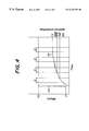
- FIG. 1 shows schematically an example of an applied voltage pattern V 1 and a temperature-rising schedule of the wafer, as a function of time past.
- a pulsed voltage between 0 and VS as a desired 10 voltage is applied.
- the voltage VS By applying the voltage VS, an attracting power enough to heat the wafer occurs and the temperature of the wafer is increased.
- the temperature When no voltage is applied, the temperature is almost constant.
- the attracting power vanishes when no voltage is applied, the wafer begin to slide relative to the attracting face and thereby the stress is released.
- the wafer's temperature difference between the successive stress releasing steps and the temperature difference between TA 4 and TS in the last stress releasing step are preferably not more than 50° C. or below, more preferably not more than 46° C. or below.
- a number of the pulse is not particularly limited, and a voltage values at high voltage applied and at low voltage applied are not restricted, but the voltage value at low voltage applied is preferably not more than the half of a desired voltage VS or below. Moreover, a negative biased voltage may be applied.
- a voltage to be applied with the electrostatic chuck may be also increased continuously to the saturated temperature.
- the treatment time can be shorten.
- FIG. 2 schematically shows, as a function of time past, an example of an applied voltage pattern V 2 and a rising schedule of the wafer's temperature in the above case.
- a voltage increasing toward the desired voltage VS is applied.
- Applying the low voltage VA 1 whereby the attracting power is increased and thereby the wafer is slid relative to the attracting face, is the stress releasing step.
- first temperature of the wafer is denoted as TO and the temperature of the stress released step is denoted as TA 5
- the difference between TA 5 and TS is preferably not more 50° C., more preferably not more than 46° C.
- the value of the low voltage VA 1 is preferably not more than the half of the desired voltage VS.
- FIG. 3 schematically shows an example of an applied voltage pattern V 3 and a rising schedule of the wafer's temperature, as a function of time past.
- the desired voltage VS is applied.
- Applying the low voltage VA 2 whereby the attracting power is decreased and the wafer is slid relative to the attracting face, is the stress releasing step.
- first temperature of the wafer is denoted as TO and the temperature of the stress releasing step is denoted as TA 6
- the temperature difference between TA 6 and TS is preferably not more than 50° C. or below, more preferably not more than 46° C. or below.
- FIG. 4 schematically show an example of an applied voltage pattern V 4 and a rising schedule of the wafer's temperature, as a function of time past.
- the desired voltage VS is applied from the beginning while the pulsed backside gas is flown intermittently during a period G.
- the wafer's temperature is smoothly increased during the period of the backside gas flowing.
- the attracting power is decreased by the pressure of the backside gas, and thereby the wafer is slid relative to the attracting face and the stress is released.
- the temperature difference between the successive stress releasing steps and the difference between the temperature TA 10 of the last stress releasing step and the saturated temperature TS are preferably not more than 50° C. or below, more preferably not more than 46° C. or below.
- the above method according to the present invention may be carried out by the following semiconductor-manufacturing equipment.
- the equipment has an electrostatic chuck with an attracting face to set a semiconductor wafer, a power source to apply a voltage with the electrostatic chuck, a controlling system to change a voltage from the power source before the semiconductor wafer's temperature arrives at the saturated temperature.
- This invention also relates to an equipment for manufacturing a semiconductor, comprising: an electrostatic chuck having an attracting face for setting a semiconductor wafer, a power supply for applying a voltage with the electrostatic chuck, a wafer's temperature-measuring means for measuring the temperature of the semiconductor wafer, and a controlling system which monitors and computes the temperature of the semiconductor wafer measured by the wafer's temperature-measuring means and transmits a controlling signal for controlling the power supply, based on the above computation.
- This invention further relates to an equipment for manufacturing a semiconductor, comprising: an electrostatic chuck having an attracting face for setting a semiconductor wafer and a dummy wafer, a power supply for applying a voltage with the electrostatic chuck, a wafer's temperature-measuring means for measuring the temperature of the dummy wafer, and a controlling system which monitors and computes the temperature of the dummy wafer measured by the wafer's temperature-measuring means and transmits a controlling signal for controlling the power supply, based on the above computation.
- an electrostatic chuck 14 to stick a wafer 16 is installed on a supporting pedestal 12 through a heater 13 in a vacuum chamber 1 . Then, a thermocouple 11 to measure the temperature of the electrostatic chuck 14 is set, and an infrared emission thermometer 7 as a wafer's temperature-measuring means for measuring the temperature of the wafer 16 . Moreover, a lift pin 15 and a lift pin-elevating equipment 9 for attracting and releasing the wafer 16 on and from the electrostatic chuck 14 .
- the wafer 16 is conveyed to the vacuum chamber 1 and set onto the lift pin 15 in above position. Thereafter, the lift pin 15 is moved downwardly by the lift pin-elevating equipment 9 and thereby the wafer 16 is set onto the electrostatic chuck 14 .
- the reference numeral “ 2 ” denotes a vacuum pump.
- the heater 13 is worked by a heater controller 5 , whereby the electrostatic chuck 14 is heated to a given temperature.
- the wafer is set onto an attracting face of the electrostatic chuck 14 and is stuck thereon by working electrostatic power sources 6 and 10 .
- the temperature of the wafer is monitored by the infrared emission thermometer 7
- the temperature of the electrostatic chuck 14 is monitored by the thermocouple 11
- the monitored data are transmitted to a controlling system 8 in a real-time.
- the controlling, as above mentioned, of the applied voltage with the electrostatic chuck and the wafer's temperature is carried out by working the controlling system 8 .
- the applied voltage with the electrostatic chuck is turn off, and the wafer 16 is released from the electrostatic chuck by moving upwardly the lift pin 15 .
- a wafer was set onto an attracting face of an electrostatic chuck, and was stuck thereon by applying a voltage in the same manner as Example 1.
- the pulsed voltage of 300V the period of the voltage was 5 seconds and the interval of the voltage was 1 second.
- Such a pulsed voltage was applied by10 cycles, turned off, and thereafter the wafer was released.
- 1700 particles with not less than 0.2 ⁇ m were observed.
- the temperature was smoothly increased as well as Example 1.
- the rise of the wafer's temperature during application of one pulsed voltage was not more than 35° C. or below and the difference between the wafer's temperature before attracting and its saturated temperature was 150° C.
- such applied voltage-schedule and a wafer's temperature-rising schedule as shown in FIG. 2 were employed, provided that VA 1 was 100V, VS was 300V, and a voltage increasing rate of 300V from 100V was 20V/min. Then, the applying voltage was held at 300V for 1 minute. After the voltage was turned off and the wafer was released, a number of particles was measured by a similar way to Example 1. Consequently, 1650 particles with not less than 0.2 ⁇ m m were observed.
- thermocouple-attached wafer When a thermocouple-attached wafer was employed and the wafer's temperature change in each position thereof at applying the voltage was measured, the difference between the wafer's temperature and its saturated temperature was 60° C. After attracting, the wafer's temperature was smoothly increased to the saturated temperature for 10 minutes.
- a wafer was stuck, released, and thereafter a number of particles on the wafer was measured in a similar way to Example 1.
- such applied voltage-schedule and a wafer's temperature-rising schedule as shown in FIG. 3 were employed, provided that VA 2 was 110V, VS was 300V, and an applying voltage was held at 300V for 1 minute. Then, 1800 particles with not less than 0.2 ⁇ m were observed.
- the wafer' temperature after 40 seconds from the beginning of the voltage application of 110V was higher by 58° C. than that before attracting. Switching the value of the voltage to 300V, the wafer's temperature was increased by 32° C. and reached the saturated temperature.
- such applied voltage-schedule and a wafer's temperature-rising schedule as shown in FIG. 4 were employed, provided that VS was 300V.
- a backside gas was introduced for 1 second so that its pressure may be 70 Torr and evacuated at 1 second later after a voltage of 300V was applied. Then, this process of gas-introduction was repeated 20 times. The wafer was released at 1 minute later after applying the above voltage. 1900 particles with not less than 0.2 ⁇ m were observed.
- the attracting power during introducing the backside gas of 70 Torr corresponds to that during applying a voltage of 110V in Example 4.
- such applied voltage-schedule and a wafer's temperature-rising schedule as shown in FIG. 4 was employed and a backside gas were not used.
- the wafer was released at 1 minute later after applying a voltage of 300V. 4500 particles with not less than 0.2 ⁇ m were observed.
- the temperature difference between before and after attracting was 69° C.
- the particles which occurs with the wafer's temperature rise after setting it onto the attracting face of the electrostatic chuck, can be reduced.
Abstract
A method for reducing particles from an electrostatic chuck, having the steps of: setting a wafer onto an attracting face of an electrostatic chuck, attracting the wafer onto the attracting face by applying a voltage to the electrostatic chuck, releasing stress due to a difference in heat expansion between the wafer and the electrostatic chuck by sliding the wafer relative to the attracting face before the wafer's temperature arrives at a saturated temperature, and increasing the wafer's temperature to a saturated temperature from its lower temperature than that of the attracting face.
Description
1. Field of the Invention
This invention relates to a method for reducing particles from an electrostatic chuck and an equipment for manufacturing a semiconductor.
2. Related Art Statement
In each step of conveying a semiconductor wafer, exposure, film-forming by CVD, sputtering, etc., micro-processing, cleaning, etching, dicing, or the like, an electrostatic chuck is employed for attracting and holding the semiconductor wafer.
Particularly, from the views of using, as an etching gas or a cleaning gas, a halogen-based corrosive gas such as ClF3, an equipment for manufacturing a semiconductor requires a high heat conduction for rapidly heating and cooling a semiconductor wafer with holding it and requires a high shock resistance not to be destroyed due to such a remarkably temperature change. Thus, a material made of dense aluminum nitride, dense alumina, or the like is promised.
On the other hand, inside the semiconductor-manufacturing equipment, the occurrence of particles, which results in defects of the semiconductor, is needed to be prevented. The particles are mainly generated from a backside surface of the semiconductor, a part of which stacks on the semiconductor wafer directly, the other part of which spreads out and stacks on a wall of a chamber. Then, the particles are peeled off of the wall, and thereby results in defects of a semiconductor.
In view of the above problems, JP A 7-245336 discloses a method in which convex-concave portions in an attracting face of an electrostatic chuck made of ceramic material are ground by irradiating a plasma and the fine protuberances of the convex-concave portions are removed, and thereby the occurrence of particles is reduced. The method is based on the finding of the cause of particles' occurrence that a silicon wafer having relatively low hardness is ground by the convex-concave portions when the silicon wafer contacts the convex-concave portions.
Moreover, JP A 8-55900 discloses a method in which a contacting shock of a silicon wafer with an electrostatic chuck is reduced by slowly rising a voltage to the electrostatic chuck when the silicon wafer is stuck to the electrostatic chuck, and thereby the particles' occurrence due to the convex-concave portions of the attracting face in the electrostatic chuck is decreased.
In a film-forming process such as a CVD or a sputtering, it is required to epitaxially grow a semiconductor film on a wafer, and thus, the wafer is required to be heated to a higher temperature range of not less than 100° C., particularly not less than 200° C. In that time, an attracting face of an electrostatic chuck is heated by a heater built-in the electrostatic chuck or a heater provided so as to be contacted with the electrostatic chuck in the lower side thereof.
In the electrostatic chuck, the wafer has a lower temperature when the wafer is stuck onto the attracting face of the electrostatic chuck, and the wafer has increasing temperature toward a saturated temperature with time past after attracting. The inventors found that, in such an electrostatic chuck or a semiconductor-manufacturing equipment, even though the contacting shock of the wafer with the electrostatic chuck just after attracting is relaxed and reduced, more particles than expectation occurs. It is difficult to reduce such particles as occurs with temperature rise of the wafer by a conventional method.
It is an object of the present invention to reduce such particles as occurs with a temperature rise of a wafer after setting the wafer onto an attracting face of an electrostatic chuck.
This invention relates to a method for reducing particles from an electrostatic chuck, comprising the steps of: setting a wafer onto an attracting face of an electrostatic chuck in a state that a temperature of the wafer is lower than that of the attracting chuck, attracting the wafer onto the attracting face by applying a voltage with the electrostatic chuck, releasing stress due to a difference in heat expansion between the wafer and the electrostatic chuck by sliding the wafer relative to the attracting face before the wafer's temperature arrives at a saturated temperature, and increasing the wafer's temperature to the saturated temperature from its lower temperature than that of the attracting face.
This invention also relates to a method for reducing particles from an electrostatic chuck, comprising the steps of: setting a wafer onto an attracting face of an electrostatic chuck, and attracting the wafer onto the attracting face by applying a pulsed voltage with the electrostatic chuck.
This invention further relates a method for reducing particles from an electrostatic chuck, comprising the steps of: setting a wafer onto an attracting face of an electrostatic chuck in a state that a temperature of the wafer is lower than that of the attracting face, and attracting the wafer onto the attracting face by applying a stepwise or continuously increasing voltage toward a saturated voltage with the electrostatic chuck.
This invention still further relate to a method for reducing particles from an electrostatic chuck, comprising the steps of: setting a wafer onto an attracting face of an electrostatic chuck, attracting the wafer into the attracting face by applying a voltage to the electrostatic chuck, and flowing a backside gas between the attracting face and the wafer when the voltage is applied to the electrostatic chuck.
This invention also relate to an equipment for manufacturing a semiconductor, comprising: an electrostatic chuck having an attracting face for setting a semiconductor wafer, a power supply for applying a voltage to the electrostatic chuck, and a backside gas-supplying equipment for flowing a backside gas between the attracting face and the wafer.
The inventors has studied to reduce particles as occurs with temperature rise of a wafer after attracting it onto an attracting face of an electrostatic chuck. Accordingly, they have got the following knowledge. That is, it has been conceived since before that the wafer have hardly stuck onto the attracting face of the electrostatic chuck made of ceramic material when the particles occur due to the shocks of the wafer colliding with the attracting face. Consequently, a means to reduce the shocks at the collision has been given. The inventors found, however, contrary to their expectations that the particles occur actually due to the difference of heat expansion between the wafer and the electrostatic chuck after the wafer is stuck onto the electrostatic chuck.
The inventors has, based on the above finding, found that a means, whereby the stresses due to the difference of the heat expansion between the wafer and the electrostatic chuck are released by sliding the wafer relative to the attracting face during the time of arriving at a given saturated temperature of the wafer from just attracting the wafer onto the electrostatic chuck, is adopted and thereby the particles are remarkably reduced.
The wording “saturated temperature” means a stable temperature of the wafer when a given heat value is afforded a system containing the wafer and the electrostatic chuck in a state that the wafer is stuck onto the electrostatic chuck with a given attracting power. Thus, when the desired attracting power or the heat value to the system changes, the saturated temperature change, too.
For a better understanding of this invention, reference is made to the attached drawings, wherein:
FIG. 1 is a graph showing, as an example, a voltage schedule V1 and a temperature schedule T1,
FIG. 2 is a graph showing, as an example, a voltage schedule V2 and a temperature schedule T2,
FIG. 3 is a graph showing, as an example, a voltage schedule V3 and a temperature schedule T3,
FIG. 4 is a graph showing, as an example, a voltage schedule V4 and a temperature schedule T4, and
FIG. 5 is a block view schematically showing a preferred embodiment for carrying out a method of the present invention.
If the temperature of the wafer increases at attracting, the difference of heat expansion between the wafer and the attracting face occurs. At that time, although a means to release the stress due to the difference of the heat expansion is not restricted, a means, in which the wafer is slid relative to the attracting face fundamentally by providing the step of decreasing the attracting power to the wafer, may be employed. The sliding can be observed with microscopic observation of the wafer's surface.
A means for reducing the attracting power to the wafer so as to cause the sliding after the attracting the wafer is begun is not restricted, the following means may be preferably used.
The means is to control an applied voltage with the electrostatic chuck. The concrete means is to apply a pulsed voltage with the electrostatic chuck. Thereby, the object of the present invention can be realized, and the temperature of the wafer can be increased during shorter time than that of only putting the wafer onto the electrostatic chuck, so that the treatment time of the wafer can be shorten.
FIG. 1 shows schematically an example of an applied voltage pattern V1 and a temperature-rising schedule of the wafer, as a function of time past. In this method, a pulsed voltage between 0 and VS as a desired 10 voltage is applied. By applying the voltage VS, an attracting power enough to heat the wafer occurs and the temperature of the wafer is increased. When no voltage is applied, the temperature is almost constant. Moreover, since the attracting power vanishes when no voltage is applied, the wafer begin to slide relative to the attracting face and thereby the stress is released. If the wafer's temperature in each of stress releasing steps is denotes as TA1 to TA4, respectively and the saturated temperature is denoted as TS, the wafer's temperature difference between the successive stress releasing steps and the temperature difference between TA4 and TS in the last stress releasing step are preferably not more than 50° C. or below, more preferably not more than 46° C. or below.
A number of the pulse is not particularly limited, and a voltage values at high voltage applied and at low voltage applied are not restricted, but the voltage value at low voltage applied is preferably not more than the half of a desired voltage VS or below. Moreover, a negative biased voltage may be applied.
A voltage to be applied with the electrostatic chuck may be also increased continuously to the saturated temperature. In this case, since the object of the present invention is attained, and besides the wafer's temperature can be increased in a short time, the treatment time can be shorten.
FIG. 2 schematically shows, as a function of time past, an example of an applied voltage pattern V2 and a rising schedule of the wafer's temperature in the above case. In this example, after low voltage VA1 is applied, a voltage increasing toward the desired voltage VS is applied. Applying the low voltage VA1, whereby the attracting power is increased and thereby the wafer is slid relative to the attracting face, is the stress releasing step. If first temperature of the wafer is denoted as TO and the temperature of the stress released step is denoted as TA5, the difference between TA5 and TS is preferably not more 50° C., more preferably not more than 46° C. Moreover, the value of the low voltage VA1 is preferably not more than the half of the desired voltage VS.
FIG. 3 schematically shows an example of an applied voltage pattern V3 and a rising schedule of the wafer's temperature, as a function of time past. In this example, after low voltage VA2 is applied, the desired voltage VS is applied. Applying the low voltage VA2, whereby the attracting power is decreased and the wafer is slid relative to the attracting face, is the stress releasing step. If first temperature of the wafer is denoted as TO and the temperature of the stress releasing step is denoted as TA6, the temperature difference between TA 6 and TS is preferably not more than 50° C. or below, more preferably not more than 46° C. or below.
Moreover, the wafer can be slid to the attracting face by flowing a backside gas between the attracting face and the wafer, when applying the voltage with the electrostatic chuck. FIG. 4 schematically show an example of an applied voltage pattern V4 and a rising schedule of the wafer's temperature, as a function of time past. In this example, the desired voltage VS is applied from the beginning while the pulsed backside gas is flown intermittently during a period G. The wafer's temperature is smoothly increased during the period of the backside gas flowing. Then, the attracting power is decreased by the pressure of the backside gas, and thereby the wafer is slid relative to the attracting face and the stress is released.
If each of temperatures of the stress releasing steps is denoted as TA1 to TA10, respectively and the saturated temperature is denoted as TS, the temperature difference between the successive stress releasing steps and the difference between the temperature TA10 of the last stress releasing step and the saturated temperature TS are preferably not more than 50° C. or below, more preferably not more than 46° C. or below.
The above method according to the present invention may be carried out by the following semiconductor-manufacturing equipment. The equipment has an electrostatic chuck with an attracting face to set a semiconductor wafer, a power source to apply a voltage with the electrostatic chuck, a controlling system to change a voltage from the power source before the semiconductor wafer's temperature arrives at the saturated temperature.
This invention also relates to an equipment for manufacturing a semiconductor, comprising: an electrostatic chuck having an attracting face for setting a semiconductor wafer, a power supply for applying a voltage with the electrostatic chuck, a wafer's temperature-measuring means for measuring the temperature of the semiconductor wafer, and a controlling system which monitors and computes the temperature of the semiconductor wafer measured by the wafer's temperature-measuring means and transmits a controlling signal for controlling the power supply, based on the above computation.
This invention further relates to an equipment for manufacturing a semiconductor, comprising: an electrostatic chuck having an attracting face for setting a semiconductor wafer and a dummy wafer, a power supply for applying a voltage with the electrostatic chuck, a wafer's temperature-measuring means for measuring the temperature of the dummy wafer, and a controlling system which monitors and computes the temperature of the dummy wafer measured by the wafer's temperature-measuring means and transmits a controlling signal for controlling the power supply, based on the above computation.
In FIG. 5, an electrostatic chuck 14 to stick a wafer 16 is installed on a supporting pedestal 12 through a heater 13 in a vacuum chamber 1. Then, a thermocouple 11 to measure the temperature of the electrostatic chuck 14 is set, and an infrared emission thermometer 7 as a wafer's temperature-measuring means for measuring the temperature of the wafer 16. Moreover, a lift pin 15 and a lift pin-elevating equipment 9 for attracting and releasing the wafer 16 on and from the electrostatic chuck 14.
The wafer 16 is conveyed to the vacuum chamber 1 and set onto the lift pin 15 in above position. Thereafter, the lift pin 15 is moved downwardly by the lift pin-elevating equipment 9 and thereby the wafer 16 is set onto the electrostatic chuck 14. The reference numeral “2” denotes a vacuum pump.
The heater 13 is worked by a heater controller 5, whereby the electrostatic chuck 14 is heated to a given temperature. The wafer is set onto an attracting face of the electrostatic chuck 14 and is stuck thereon by working electrostatic power sources 6 and 10. In this case, the temperature of the wafer is monitored by the infrared emission thermometer 7, the temperature of the electrostatic chuck 14 is monitored by the thermocouple 11, and thereafter the monitored data are transmitted to a controlling system 8 in a real-time. The controlling, as above mentioned, of the applied voltage with the electrostatic chuck and the wafer's temperature is carried out by working the controlling system 8.
After film-forming, the applied voltage with the electrostatic chuck is turn off, and the wafer 16 is released from the electrostatic chuck by moving upwardly the lift pin 15.
By employing such an equipment as FIG. 5 and followed by such a voltage schedule as FIG. 1, a wafer is stuck. Then, the wafer was conveyed to a vacuum chamber in a pressure of 10−5 Torr. When the wafer's temperature TO just before attracting was measured by an infrared emission thermometer, the temperature was 246° C. The temperature of the electrostatic chuck was made to be 320° C. in stable and the wafer with a dimension of 8 inches was set onto its attracting face. In this case, a mirror face of the wafer was downward. Such pulsed voltage as shown in FIG. 1 was applied to an electrode inside the electrostatic chuck, provided that the VS was 300V, the applying period of the 300V pulsed voltage was 4 seconds, and the interval of the pulsed voltage was 1 second. The pulsed voltage was applied by 12 pulses, and thereafter the wafer was released from the electrostatic chuck.
When a number of particles on the wafer was measured by a wafer protractor (WM-1500 made by Topcon Co., Ltd), 1500 particles with not less than 0.2 μm were observed. Moreover, a wafer with a thermocouple (8 inches' dimension, 17 measuring points) was employed, and the temperature change of the wafer was measured by applying a voltage, followed by a similar process to the above mentioned. When a voltage of 300V is applied for 4 seconds, the wafer's temperature is increased by 20° C. as compared with that before attracting. When the voltage is not applied for 1 second, the wafer's temperature is not decreased. After the above process, the wafer's temperature is almost smoothly increased during voltage application and arrive at a saturated temperature of 307° C. The rise of the wafer's temperature during application of one pulsed voltage was not more than 20° C. or below.
A wafer was set onto an attracting face of an electrostatic chuck, and was stuck thereon by applying a voltage in the same manner as Example 1. Hereupon, in applying the pulsed voltage of 300V , the period of the voltage was 5 seconds and the interval of the voltage was 1 second. Such a pulsed voltage was applied by10 cycles, turned off, and thereafter the wafer was released. When a number of particles was measured in a similar way to Example 1, 1700 particles with not less than 0.2 μm were observed. Moreover, when a thermocouple-attached wafer was employed and the temperature change in each point of the wafer was measured, the temperature was smoothly increased as well as Example 1. The rise of the wafer's temperature during application of one pulsed voltage was not more than 35° C. or below and the difference between the wafer's temperature before attracting and its saturated temperature was 150° C.
A wafer was stuck, released, and thereafter a number of particles on the wafer was measured in a similar way to Example 1. Hereupon, such applied voltage-schedule and a wafer's temperature-rising schedule as shown in FIG. 2 were employed, provided that VA1 was 100V, VS was 300V, and a voltage increasing rate of 300V from 100V was 20V/min. Then, the applying voltage was held at 300V for 1 minute. After the voltage was turned off and the wafer was released, a number of particles was measured by a similar way to Example 1. Consequently, 1650 particles with not less than 0.2 μm m were observed.
When a thermocouple-attached wafer was employed and the wafer's temperature change in each position thereof at applying the voltage was measured, the difference between the wafer's temperature and its saturated temperature was 60° C. After attracting, the wafer's temperature was smoothly increased to the saturated temperature for 10 minutes.
A wafer was stuck, released, and thereafter a number of particles on the wafer was measured in a similar way to Example 1. Hereupon, such applied voltage-schedule and a wafer's temperature-rising schedule as shown in FIG. 3 were employed, provided that VA2 was 110V, VS was 300V, and an applying voltage was held at 300V for 1 minute. Then, 1800 particles with not less than 0.2 μm were observed.
When a thermocouple-attached wafer was employed and the wafer's temperature change in each position thereof at applying the voltage was measured, the wafer' temperature after 40 seconds from the beginning of the voltage application of 110V was higher by 58° C. than that before attracting. Switching the value of the voltage to 300V, the wafer's temperature was increased by 32° C. and reached the saturated temperature.
A wafer was stuck, released, and thereafter a number of particles on the wafer was measured in a similar way to Example 1. Hereupon, such applied voltage-schedule and a wafer's temperature-rising schedule as shown in FIG. 4 were employed, provided that VS was 300V. Moreover, in this case, a backside gas was introduced for 1 second so that its pressure may be 70 Torr and evacuated at 1 second later after a voltage of 300V was applied. Then, this process of gas-introduction was repeated 20 times. The wafer was released at 1 minute later after applying the above voltage. 1900 particles with not less than 0.2 μm were observed.
The attracting power during introducing the backside gas of 70 Torr corresponds to that during applying a voltage of 110V in Example 4.
A wafer was stuck, released, and thereafter a number of particles on the wafer was measured in a similar way to Example 1. Hereupon, such applied voltage-schedule and a wafer's temperature-rising schedule as shown in FIG. 4 was employed and a backside gas were not used. The wafer was released at 1 minute later after applying a voltage of 300V. 4500 particles with not less than 0.2 μm were observed. The temperature difference between before and after attracting was 69° C.
As above mentioned, according to the present invention, the particles, which occurs with the wafer's temperature rise after setting it onto the attracting face of the electrostatic chuck, can be reduced.
Claims (7)
1. A method for reducing particles from an electrostatic chuck, comprising:
providing an electrostatic chuck with an attracting face,
setting a wafer onto the attracting face of the electrostatic chuck in a state wherein the temperature of the wafer is lower than the temperature of the attracting face,
attracting the wafer onto the attracting face by applying a voltage to the electrostatic chuck,
releasing stress due to a difference of the heat expansion between the wafer and the electrostatic chuck by sliding the wafer relative to the attracting face before the temperature of the wafer arrives at a saturated temperature, and
increasing the temperature of the wafer to a saturated temperature.
2. The method of claim 1, wherein the sliding of the wafer relative to the attracting face is controlled by the voltage to be applied to the electrostatic chuck.
3. The method of claim 2, wherein the voltage is a pulsed voltage.
4. The method of claim 2, wherein the voltage is increased stepwise to reach the saturated temperature.
5. The method of claim 2, wherein the voltage is increased continuously to reach the saturated temperature.
6. The method of claim 1, wherein the wafer is sliding relative to the attractive face by reducing an attracting power of the electrostatic chuck to the wafer through flowing a backside gas between the attracting face and the wafer when the voltage is applied to the electrostatic chuck.
7. The method of claim 1, wherein a difference between the saturated temperature and the temperature of the wafer in a last stress releasing step before the wafer reaches the saturated temperature is 50 °C. or below.
Priority Applications (1)
| Application Number | Priority Date | Filing Date | Title |
|---|---|---|---|
| US09/769,519 US6975497B2 (en) | 1998-07-06 | 2001-01-26 | Method for reducing particles from an electrostatic chuck and an equipment for manufacturing a semiconductor |
Applications Claiming Priority (2)
| Application Number | Priority Date | Filing Date | Title |
|---|---|---|---|
| JP10-190350 | 1998-07-06 | ||
| JP10190350A JP2000021964A (en) | 1998-07-06 | 1998-07-06 | Electrostatic chuck particle reducing method and semiconductor manufacturing apparatus |
Related Child Applications (1)
| Application Number | Title | Priority Date | Filing Date |
|---|---|---|---|
| US09/769,519 Continuation US6975497B2 (en) | 1998-07-06 | 2001-01-26 | Method for reducing particles from an electrostatic chuck and an equipment for manufacturing a semiconductor |
Publications (1)
| Publication Number | Publication Date |
|---|---|
| US6252758B1 true US6252758B1 (en) | 2001-06-26 |
Family
ID=16256740
Family Applications (2)
| Application Number | Title | Priority Date | Filing Date |
|---|---|---|---|
| US09/346,305 Expired - Fee Related US6252758B1 (en) | 1998-07-06 | 1999-07-02 | Method for reducing particles from an electrostatic chuck and an equipment for manufacturing a semiconductor |
| US09/769,519 Expired - Fee Related US6975497B2 (en) | 1998-07-06 | 2001-01-26 | Method for reducing particles from an electrostatic chuck and an equipment for manufacturing a semiconductor |
Family Applications After (1)
| Application Number | Title | Priority Date | Filing Date |
|---|---|---|---|
| US09/769,519 Expired - Fee Related US6975497B2 (en) | 1998-07-06 | 2001-01-26 | Method for reducing particles from an electrostatic chuck and an equipment for manufacturing a semiconductor |
Country Status (6)
| Country | Link |
|---|---|
| US (2) | US6252758B1 (en) |
| EP (1) | EP0971391B1 (en) |
| JP (1) | JP2000021964A (en) |
| KR (2) | KR100353021B1 (en) |
| DE (1) | DE69927439T2 (en) |
| TW (1) | TW417146B (en) |
Cited By (11)
| Publication number | Priority date | Publication date | Assignee | Title |
|---|---|---|---|---|
| US20020153024A1 (en) * | 2001-03-19 | 2002-10-24 | Fuminori Akiba | Electrostatic chuck cleaning method |
| US6778377B2 (en) * | 2000-06-22 | 2004-08-17 | Renesas Technology Corp. | Electrostatic chucking system, and apparatus and method of manufacturing a semiconductor device using the electrostatic chucking system |
| US20050174135A1 (en) * | 2002-06-17 | 2005-08-11 | Ryuichi Matsuda | Method and device for measuring wafer potential or temperature |
| US6975497B2 (en) * | 1998-07-06 | 2005-12-13 | Ngk Insulators, Ltd. | Method for reducing particles from an electrostatic chuck and an equipment for manufacturing a semiconductor |
| US20080314733A1 (en) * | 2007-06-22 | 2008-12-25 | Lam Research Corporation | Methods of and apparatus for reducing amounts of particles on a wafer during wafer de-chucking |
| US20090059199A1 (en) * | 2007-09-04 | 2009-03-05 | Asml Netherlands B.V. | Method of loading a substrate on a substrate table and lithographic apparatus and device manufacturing method |
| US20100195080A1 (en) * | 2007-06-21 | 2010-08-05 | Asml Netherlands B.V. | Clamping Device And Object Loading Method |
| US8338272B2 (en) | 2008-08-29 | 2012-12-25 | Renesas Electronics Corporation | Method for manufacturing a semiconductor device |
| US8835327B2 (en) | 2012-03-15 | 2014-09-16 | Fujitsu Limited | Method of manufacturing semiconductor device |
| US20180366359A1 (en) * | 2017-06-20 | 2018-12-20 | Applied Materials, Inc. | Method and apparatus for de-chucking a workpiece using a swing voltage sequence |
| US20220359172A1 (en) * | 2014-12-16 | 2022-11-10 | Hitachi High-Tech Corporation | Plasma processing apparatus |
Families Citing this family (21)
| Publication number | Priority date | Publication date | Assignee | Title |
|---|---|---|---|---|
| JP2002009141A (en) * | 2000-06-26 | 2002-01-11 | Anelva Corp | Vacuum treatment apparatus having electrostatic attraction mechanism and operation control method for electrostatic attraction mechanism |
| US7073217B2 (en) * | 2004-11-24 | 2006-07-11 | Stevenson Edward F | Folding multimodal sofa beds for recreational vehicles |
| US20080180873A1 (en) * | 2007-01-31 | 2008-07-31 | Applied Materials, Inc. | Securing a substrate to an electrostatic chuck |
| US20080316461A1 (en) * | 2007-06-21 | 2008-12-25 | Asml Netherlands B.V. | Lithographic apparatus and device manufacturing method |
| TWI448826B (en) * | 2007-06-21 | 2014-08-11 | Asml Netherlands Bv | Method of loading a substrate on a substrate table, device manufacturing method, computer program, data carrier and apparatus |
| US20090086187A1 (en) * | 2007-08-09 | 2009-04-02 | Asml Netherlands | Lithographic Apparatus and Device Manufacturing Method |
| US20090109595A1 (en) * | 2007-10-31 | 2009-04-30 | Sokudo Co., Ltd. | Method and system for performing electrostatic chuck clamping in track lithography tools |
| US9991147B2 (en) * | 2009-09-01 | 2018-06-05 | Hermes Microvision, Inc. | Wafer grounding and biasing method, apparatus, and application |
| US9399812B2 (en) * | 2011-10-11 | 2016-07-26 | Applied Materials, Inc. | Methods of preventing plasma induced damage during substrate processing |
| JP5933222B2 (en) * | 2011-11-08 | 2016-06-08 | 東京エレクトロン株式会社 | Temperature control method, control device, and plasma processing apparatus |
| JP6202720B2 (en) * | 2013-03-29 | 2017-09-27 | 株式会社日立ハイテクノロジーズ | Plasma processing apparatus and plasma processing method |
| JP6075555B2 (en) * | 2013-07-05 | 2017-02-08 | 日新イオン機器株式会社 | Electrostatic chuck system and semiconductor manufacturing apparatus |
| US9530626B2 (en) | 2014-07-25 | 2016-12-27 | Tokyo Electron Limited | Method and apparatus for ESC charge control for wafer clamping |
| US9570272B2 (en) * | 2015-03-31 | 2017-02-14 | Panasonic Intellectual Property Management Co., Ltd. | Plasma processing apparatus and plasma processing method |
| WO2017182216A1 (en) * | 2016-04-20 | 2017-10-26 | Asml Netherlands B.V. | Substrate support, lithographic apparatus and loading method |
| JP7304188B2 (en) | 2019-03-29 | 2023-07-06 | 東京エレクトロン株式会社 | Substrate processing method and substrate processing apparatus |
| JP7341043B2 (en) | 2019-12-06 | 2023-09-08 | 東京エレクトロン株式会社 | Substrate processing method and substrate processing apparatus |
| US11607716B1 (en) | 2020-06-23 | 2023-03-21 | Kla Corporation | Systems and methods for chuck cleaning |
| CN115621185A (en) * | 2021-07-13 | 2023-01-17 | 长鑫存储技术有限公司 | Control method and control system of deposition equipment |
| CN113628958B (en) * | 2021-07-29 | 2024-04-23 | 华虹半导体(无锡)有限公司 | Method for manufacturing semiconductor device |
| CN114400174B (en) * | 2022-01-18 | 2023-10-20 | 长鑫存储技术有限公司 | Plasma processing device and method for processing wafer |
Citations (11)
| Publication number | Priority date | Publication date | Assignee | Title |
|---|---|---|---|---|
| JPS59181622A (en) * | 1983-03-31 | 1984-10-16 | Fujitsu Ltd | Manufacture of semiconductor device |
| US5320982A (en) * | 1990-07-02 | 1994-06-14 | Hitachi, Ltd. | Wafer cooling method and apparatus |
| JPH07245336A (en) | 1994-03-03 | 1995-09-19 | Fujitsu Ltd | Electrostatic chuck and its surface treating method |
| JPH0855900A (en) | 1994-08-11 | 1996-02-27 | Fujitsu Ltd | Electrostatic attraction method and its device and manufacture of semiconductor device |
| JPH08316297A (en) * | 1995-05-24 | 1996-11-29 | Sony Corp | Electrostatic chuck and its controlling method |
| US5746928A (en) * | 1996-06-03 | 1998-05-05 | Taiwan Semiconductor Manufacturing Company Ltd | Process for cleaning an electrostatic chuck of a plasma etching apparatus |
| US5793192A (en) * | 1996-06-28 | 1998-08-11 | Lam Research Corporation | Methods and apparatuses for clamping and declamping a semiconductor wafer in a wafer processing system |
| JPH1167883A (en) * | 1997-08-14 | 1999-03-09 | Sony Corp | Electrostatic chuck |
| US5910011A (en) * | 1997-05-12 | 1999-06-08 | Applied Materials, Inc. | Method and apparatus for monitoring processes using multiple parameters of a semiconductor wafer processing system |
| JPH11251418A (en) * | 1998-03-02 | 1999-09-17 | Ulvac Corp | Vacuum process |
| US6084763A (en) * | 1996-06-21 | 2000-07-04 | Sony Corporation | Method of holding wafer, method of removing wafer and electrostatic chucking device |
Family Cites Families (19)
| Publication number | Priority date | Publication date | Assignee | Title |
|---|---|---|---|---|
| JPH0640027B2 (en) * | 1985-11-07 | 1994-05-25 | 光洋リンドバ−グ株式会社 | Method for measuring the temperature of an object to be heated in an optical heat treatment apparatus |
| US5147498A (en) * | 1990-04-09 | 1992-09-15 | Anelva Corporation | Apparatus for controlling temperature in the processing of a substrate |
| JP2939771B2 (en) | 1990-04-09 | 1999-08-25 | アネルバ 株式会社 | Semiconductor wafer processing method and apparatus |
| JPH04206546A (en) * | 1990-11-30 | 1992-07-28 | Hitachi Ltd | Method and device for plasma treatment |
| US5325261A (en) * | 1991-05-17 | 1994-06-28 | Unisearch Limited | Electrostatic chuck with improved release |
| JP2941572B2 (en) * | 1992-08-11 | 1999-08-25 | 三菱電機株式会社 | Plasma etching apparatus and method for manufacturing semiconductor device |
| JPH06151568A (en) * | 1992-11-02 | 1994-05-31 | Nippon Steel Corp | Electrostatic chuck device |
| TW277139B (en) * | 1993-09-16 | 1996-06-01 | Hitachi Seisakusyo Kk | |
| US5459632A (en) * | 1994-03-07 | 1995-10-17 | Applied Materials, Inc. | Releasing a workpiece from an electrostatic chuck |
| JP3451410B2 (en) * | 1994-10-07 | 2003-09-29 | 富士通株式会社 | Dry etching method |
| JP4079992B2 (en) * | 1994-10-17 | 2008-04-23 | バリアン・セミコンダクター・エクイップメント・アソシエイツ・インコーポレイテッド | Apparatus and electrostatic clamping method for fastening conductive object to mounting member |
| JPH08191098A (en) * | 1995-01-09 | 1996-07-23 | Hitachi Ltd | Electrostatic attraction equipment |
| JPH08213362A (en) * | 1995-02-02 | 1996-08-20 | Sony Corp | Plasma treatment equipment and plasma treatment method |
| US5982986A (en) * | 1995-02-03 | 1999-11-09 | Applied Materials, Inc. | Apparatus and method for rotationally aligning and degassing semiconductor substrate within single vacuum chamber |
| US6140612A (en) * | 1995-06-07 | 2000-10-31 | Lam Research Corporation | Controlling the temperature of a wafer by varying the pressure of gas between the underside of the wafer and the chuck |
| JP3563224B2 (en) * | 1996-03-25 | 2004-09-08 | 住友電気工業株式会社 | Semiconductor wafer evaluation method, heat treatment method, and heat treatment apparatus |
| TW334609B (en) * | 1996-09-19 | 1998-06-21 | Hitachi Ltd | Electrostatic chuck, method and device for processing sanyle use the same |
| JPH09191005A (en) * | 1996-12-26 | 1997-07-22 | Hitachi Ltd | Specimen temperature control method and vacuum treatment apparatus |
| JP2000021964A (en) * | 1998-07-06 | 2000-01-21 | Ngk Insulators Ltd | Electrostatic chuck particle reducing method and semiconductor manufacturing apparatus |
-
1998
- 1998-07-06 JP JP10190350A patent/JP2000021964A/en active Pending
-
1999
- 1999-06-22 TW TW088110442A patent/TW417146B/en not_active IP Right Cessation
- 1999-07-02 KR KR1019990026459A patent/KR100353021B1/en not_active IP Right Cessation
- 1999-07-02 US US09/346,305 patent/US6252758B1/en not_active Expired - Fee Related
- 1999-07-05 EP EP99305306A patent/EP0971391B1/en not_active Expired - Lifetime
- 1999-07-05 DE DE69927439T patent/DE69927439T2/en not_active Expired - Lifetime
-
2001
- 2001-01-26 US US09/769,519 patent/US6975497B2/en not_active Expired - Fee Related
- 2001-06-22 KR KR10-2001-0035649A patent/KR100412119B1/en not_active IP Right Cessation
Patent Citations (11)
| Publication number | Priority date | Publication date | Assignee | Title |
|---|---|---|---|---|
| JPS59181622A (en) * | 1983-03-31 | 1984-10-16 | Fujitsu Ltd | Manufacture of semiconductor device |
| US5320982A (en) * | 1990-07-02 | 1994-06-14 | Hitachi, Ltd. | Wafer cooling method and apparatus |
| JPH07245336A (en) | 1994-03-03 | 1995-09-19 | Fujitsu Ltd | Electrostatic chuck and its surface treating method |
| JPH0855900A (en) | 1994-08-11 | 1996-02-27 | Fujitsu Ltd | Electrostatic attraction method and its device and manufacture of semiconductor device |
| JPH08316297A (en) * | 1995-05-24 | 1996-11-29 | Sony Corp | Electrostatic chuck and its controlling method |
| US5746928A (en) * | 1996-06-03 | 1998-05-05 | Taiwan Semiconductor Manufacturing Company Ltd | Process for cleaning an electrostatic chuck of a plasma etching apparatus |
| US6084763A (en) * | 1996-06-21 | 2000-07-04 | Sony Corporation | Method of holding wafer, method of removing wafer and electrostatic chucking device |
| US5793192A (en) * | 1996-06-28 | 1998-08-11 | Lam Research Corporation | Methods and apparatuses for clamping and declamping a semiconductor wafer in a wafer processing system |
| US5910011A (en) * | 1997-05-12 | 1999-06-08 | Applied Materials, Inc. | Method and apparatus for monitoring processes using multiple parameters of a semiconductor wafer processing system |
| JPH1167883A (en) * | 1997-08-14 | 1999-03-09 | Sony Corp | Electrostatic chuck |
| JPH11251418A (en) * | 1998-03-02 | 1999-09-17 | Ulvac Corp | Vacuum process |
Cited By (22)
| Publication number | Priority date | Publication date | Assignee | Title |
|---|---|---|---|---|
| US6975497B2 (en) * | 1998-07-06 | 2005-12-13 | Ngk Insulators, Ltd. | Method for reducing particles from an electrostatic chuck and an equipment for manufacturing a semiconductor |
| US6778377B2 (en) * | 2000-06-22 | 2004-08-17 | Renesas Technology Corp. | Electrostatic chucking system, and apparatus and method of manufacturing a semiconductor device using the electrostatic chucking system |
| US20020153024A1 (en) * | 2001-03-19 | 2002-10-24 | Fuminori Akiba | Electrostatic chuck cleaning method |
| US7004180B2 (en) * | 2001-03-19 | 2006-02-28 | Applied Materials, Inc. | Electrostatic chuck cleaning method |
| US20060112970A1 (en) * | 2001-03-19 | 2006-06-01 | Applied Materials, Inc. | Electrostatic chuck cleaning method |
| US8454758B2 (en) | 2001-03-19 | 2013-06-04 | Applied Materials, Inc. | Electrostatic chuck cleaning method |
| US20050174135A1 (en) * | 2002-06-17 | 2005-08-11 | Ryuichi Matsuda | Method and device for measuring wafer potential or temperature |
| US7335315B2 (en) * | 2002-06-17 | 2008-02-26 | Mitsubishi Heavy Industries, Ltd. | Method and device for measuring wafer potential or temperature |
| US20100195080A1 (en) * | 2007-06-21 | 2010-08-05 | Asml Netherlands B.V. | Clamping Device And Object Loading Method |
| US9013682B2 (en) | 2007-06-21 | 2015-04-21 | Asml Netherlands B.V. | Clamping device and object loading method |
| WO2009002415A1 (en) * | 2007-06-22 | 2008-12-31 | Lam Research Corporation | Methods of and apparatus for reducing amounts of particles on a wafer during wafer de-chucking |
| US7782591B2 (en) | 2007-06-22 | 2010-08-24 | Lam Research Corporation | Methods of and apparatus for reducing amounts of particles on a wafer during wafer de-chucking |
| US20080314733A1 (en) * | 2007-06-22 | 2008-12-25 | Lam Research Corporation | Methods of and apparatus for reducing amounts of particles on a wafer during wafer de-chucking |
| US9122174B2 (en) | 2007-09-04 | 2015-09-01 | Asml Netherlands B.V. | Method of loading a substrate on a substrate table and lithographic apparatus and device manufacturing method |
| US8446566B2 (en) | 2007-09-04 | 2013-05-21 | Asml Netherlands B.V. | Method of loading a substrate on a substrate table and lithographic apparatus and device manufacturing method |
| US20090059199A1 (en) * | 2007-09-04 | 2009-03-05 | Asml Netherlands B.V. | Method of loading a substrate on a substrate table and lithographic apparatus and device manufacturing method |
| US8338272B2 (en) | 2008-08-29 | 2012-12-25 | Renesas Electronics Corporation | Method for manufacturing a semiconductor device |
| US8835327B2 (en) | 2012-03-15 | 2014-09-16 | Fujitsu Limited | Method of manufacturing semiconductor device |
| US20220359172A1 (en) * | 2014-12-16 | 2022-11-10 | Hitachi High-Tech Corporation | Plasma processing apparatus |
| US20180366359A1 (en) * | 2017-06-20 | 2018-12-20 | Applied Materials, Inc. | Method and apparatus for de-chucking a workpiece using a swing voltage sequence |
| US10242893B2 (en) * | 2017-06-20 | 2019-03-26 | Applied Materials, Inc. | Method and apparatus for de-chucking a workpiece using a swing voltage sequence |
| US10784132B2 (en) | 2017-06-20 | 2020-09-22 | Applied Materials, Inc. | Method and apparatus for de-chucking a workpiece using a swing voltage sequence |
Also Published As
| Publication number | Publication date |
|---|---|
| KR100353021B1 (en) | 2002-09-16 |
| EP0971391A3 (en) | 2002-10-02 |
| TW417146B (en) | 2001-01-01 |
| US6975497B2 (en) | 2005-12-13 |
| EP0971391B1 (en) | 2005-09-28 |
| KR20010070935A (en) | 2001-07-27 |
| DE69927439T2 (en) | 2006-06-22 |
| JP2000021964A (en) | 2000-01-21 |
| EP0971391A2 (en) | 2000-01-12 |
| DE69927439D1 (en) | 2006-02-09 |
| KR100412119B1 (en) | 2003-12-24 |
| US20010002871A1 (en) | 2001-06-07 |
| KR20000011428A (en) | 2000-02-25 |
Similar Documents
| Publication | Publication Date | Title |
|---|---|---|
| US6252758B1 (en) | Method for reducing particles from an electrostatic chuck and an equipment for manufacturing a semiconductor | |
| JP6526729B6 (en) | Rare earth oxide based monolithic chamber material | |
| JP5111030B2 (en) | Temperature controlled substrate holder with an erosion resistant insulating layer for use in a substrate processing system | |
| KR100984309B1 (en) | Plasma processing apparatus and plasma processing method | |
| KR100790765B1 (en) | Method for heating a semiconductor wafer in a process chamber, and process chamber | |
| US6905984B2 (en) | MEMS based contact conductivity electrostatic chuck | |
| JPH11507473A (en) | Wafer temperature control method and apparatus | |
| DE60313861D1 (en) | CHANGEABLE TEMPERATURE PROCESSES FOR ADJUSTABLE ELECTROSTATIC SUBSTRATE HOLDER | |
| WO2006130573A2 (en) | Optimizing the thermal budget during a pulsed heating process | |
| WO2010068294A1 (en) | Electrostatic chuck with compliant coat | |
| US6549392B1 (en) | Method for reducing particles from an electrostatic chuck and an equipment for manufacturing a semiconductor | |
| US6831823B2 (en) | Method and apparatus for chucking a substrate | |
| US20110104363A1 (en) | Plasma processing apparatus and method for controlling substrate attraction force in plasma processing apparatus | |
| US6759624B2 (en) | Method and apparatus for heating a semiconductor wafer plasma reactor vacuum chamber | |
| TWI534939B (en) | Methods for stabilizing contact surfaces of electrostatic chucks | |
| US10896840B2 (en) | Tape heating methods | |
| JP2613296B2 (en) | Vacuum processing method and device | |
| JPH02270320A (en) | Method and device of surface treatment | |
| KR100763681B1 (en) | Device and method for controlling the high density plasma chemical vapor deposition | |
| TW202221841A (en) | Hybrid high-temperature electrostatic clamp for improved workpiece temperature uniformity | |
| KR20040011840A (en) | Device and Method for manufacturing semiconductor devices with Electrostatic chuck | |
| WO2016176566A1 (en) | Methods and apparatus for correcting substrate deformity | |
| JP2613296C (en) |
Legal Events
| Date | Code | Title | Description |
|---|---|---|---|
| AS | Assignment |
Owner name: NGK INSULATORS, LTD., JAPAN Free format text: ASSIGNMENT OF ASSIGNORS INTEREST;ASSIGNORS:NAGAO, MIE;USHIKOSHI, RYUSUKE;OHNO, MASASHI;REEL/FRAME:010127/0526 Effective date: 19990713 |
|
| FPAY | Fee payment |
Year of fee payment: 4 |
|
| FPAY | Fee payment |
Year of fee payment: 8 |
|
| REMI | Maintenance fee reminder mailed | ||
| LAPS | Lapse for failure to pay maintenance fees | ||
| STCH | Information on status: patent discontinuation |
Free format text: PATENT EXPIRED DUE TO NONPAYMENT OF MAINTENANCE FEES UNDER 37 CFR 1.362 |
|
| FP | Lapsed due to failure to pay maintenance fee |
Effective date: 20130626 |