US6163519A - Scanning near-field optical microscope using the probe and recording and/or reproducing apparatus using the probe - Google Patents
Scanning near-field optical microscope using the probe and recording and/or reproducing apparatus using the probe Download PDFInfo
- Publication number
- US6163519A US6163519A US09/518,104 US51810400A US6163519A US 6163519 A US6163519 A US 6163519A US 51810400 A US51810400 A US 51810400A US 6163519 A US6163519 A US 6163519A
- Authority
- US
- United States
- Prior art keywords
- probe
- minute aperture
- probes
- light
- tip
- Prior art date
- Legal status (The legal status is an assumption and is not a legal conclusion. Google has not performed a legal analysis and makes no representation as to the accuracy of the status listed.)
- Expired - Fee Related
Links
Images


Classifications
-
- G—PHYSICS
- G01—MEASURING; TESTING
- G01Q—SCANNING-PROBE TECHNIQUES OR APPARATUS; APPLICATIONS OF SCANNING-PROBE TECHNIQUES, e.g. SCANNING PROBE MICROSCOPY [SPM]
- G01Q60/00—Particular types of SPM [Scanning Probe Microscopy] or microscopes; Essential components thereof
- G01Q60/18—SNOM [Scanning Near-Field Optical Microscopy] or apparatus therefor, e.g. SNOM probes
- G01Q60/22—Probes, their manufacture, or their related instrumentation, e.g. holders
-
- G—PHYSICS
- G01—MEASURING; TESTING
- G01Q—SCANNING-PROBE TECHNIQUES OR APPARATUS; APPLICATIONS OF SCANNING-PROBE TECHNIQUES, e.g. SCANNING PROBE MICROSCOPY [SPM]
- G01Q70/00—General aspects of SPM probes, their manufacture or their related instrumentation, insofar as they are not specially adapted to a single SPM technique covered by group G01Q60/00
- G01Q70/06—Probe tip arrays
-
- G—PHYSICS
- G02—OPTICS
- G02B—OPTICAL ELEMENTS, SYSTEMS OR APPARATUS
- G02B6/00—Light guides; Structural details of arrangements comprising light guides and other optical elements, e.g. couplings
- G02B6/10—Light guides; Structural details of arrangements comprising light guides and other optical elements, e.g. couplings of the optical waveguide type
- G02B6/12—Light guides; Structural details of arrangements comprising light guides and other optical elements, e.g. couplings of the optical waveguide type of the integrated circuit kind
- G02B6/122—Basic optical elements, e.g. light-guiding paths
-
- G—PHYSICS
- G11—INFORMATION STORAGE
- G11B—INFORMATION STORAGE BASED ON RELATIVE MOVEMENT BETWEEN RECORD CARRIER AND TRANSDUCER
- G11B11/00—Recording on or reproducing from the same record carrier wherein for these two operations the methods are covered by different main groups of groups G11B3/00 - G11B7/00 or by different subgroups of group G11B9/00; Record carriers therefor
- G11B11/03—Recording on or reproducing from the same record carrier wherein for these two operations the methods are covered by different main groups of groups G11B3/00 - G11B7/00 or by different subgroups of group G11B9/00; Record carriers therefor using recording by deforming with non-mechanical means, e.g. laser, beam of particles
-
- G—PHYSICS
- G11—INFORMATION STORAGE
- G11B—INFORMATION STORAGE BASED ON RELATIVE MOVEMENT BETWEEN RECORD CARRIER AND TRANSDUCER
- G11B7/00—Recording or reproducing by optical means, e.g. recording using a thermal beam of optical radiation by modifying optical properties or the physical structure, reproducing using an optical beam at lower power by sensing optical properties; Record carriers therefor
- G11B7/004—Recording, reproducing or erasing methods; Read, write or erase circuits therefor
- G11B7/005—Reproducing
-
- G—PHYSICS
- G11—INFORMATION STORAGE
- G11B—INFORMATION STORAGE BASED ON RELATIVE MOVEMENT BETWEEN RECORD CARRIER AND TRANSDUCER
- G11B7/00—Recording or reproducing by optical means, e.g. recording using a thermal beam of optical radiation by modifying optical properties or the physical structure, reproducing using an optical beam at lower power by sensing optical properties; Record carriers therefor
- G11B7/12—Heads, e.g. forming of the optical beam spot or modulation of the optical beam
- G11B7/14—Heads, e.g. forming of the optical beam spot or modulation of the optical beam specially adapted to record on, or to reproduce from, more than one track simultaneously
-
- G—PHYSICS
- G11—INFORMATION STORAGE
- G11B—INFORMATION STORAGE BASED ON RELATIVE MOVEMENT BETWEEN RECORD CARRIER AND TRANSDUCER
- G11B7/00—Recording or reproducing by optical means, e.g. recording using a thermal beam of optical radiation by modifying optical properties or the physical structure, reproducing using an optical beam at lower power by sensing optical properties; Record carriers therefor
- G11B7/12—Heads, e.g. forming of the optical beam spot or modulation of the optical beam
- G11B7/22—Apparatus or processes for the manufacture of optical heads, e.g. assembly
-
- G—PHYSICS
- G11—INFORMATION STORAGE
- G11B—INFORMATION STORAGE BASED ON RELATIVE MOVEMENT BETWEEN RECORD CARRIER AND TRANSDUCER
- G11B9/00—Recording or reproducing using a method not covered by one of the main groups G11B3/00 - G11B7/00; Record carriers therefor
- G11B9/12—Recording or reproducing using a method not covered by one of the main groups G11B3/00 - G11B7/00; Record carriers therefor using near-field interactions; Record carriers therefor
- G11B9/14—Recording or reproducing using a method not covered by one of the main groups G11B3/00 - G11B7/00; Record carriers therefor using near-field interactions; Record carriers therefor using microscopic probe means, i.e. recording or reproducing by means directly associated with the tip of a microscopic electrical probe as used in Scanning Tunneling Microscopy [STM] or Atomic Force Microscopy [AFM] for inducing physical or electrical perturbations in a recording medium; Record carriers or media specially adapted for such transducing of information
- G11B9/1409—Heads
-
- G—PHYSICS
- G01—MEASURING; TESTING
- G01Q—SCANNING-PROBE TECHNIQUES OR APPARATUS; APPLICATIONS OF SCANNING-PROBE TECHNIQUES, e.g. SCANNING PROBE MICROSCOPY [SPM]
- G01Q80/00—Applications, other than SPM, of scanning-probe techniques
-
- Y—GENERAL TAGGING OF NEW TECHNOLOGICAL DEVELOPMENTS; GENERAL TAGGING OF CROSS-SECTIONAL TECHNOLOGIES SPANNING OVER SEVERAL SECTIONS OF THE IPC; TECHNICAL SUBJECTS COVERED BY FORMER USPC CROSS-REFERENCE ART COLLECTIONS [XRACs] AND DIGESTS
- Y10—TECHNICAL SUBJECTS COVERED BY FORMER USPC
- Y10S—TECHNICAL SUBJECTS COVERED BY FORMER USPC CROSS-REFERENCE ART COLLECTIONS [XRACs] AND DIGESTS
- Y10S977/00—Nanotechnology
- Y10S977/84—Manufacture, treatment, or detection of nanostructure
- Y10S977/849—Manufacture, treatment, or detection of nanostructure with scanning probe
- Y10S977/86—Scanning probe structure
- Y10S977/862—Near-field probe
Definitions
- the present invention relates to a method of manufacturing or producing a probe with a minute aperture suitable for use in a scanning near-field optical microscope, an information recording and/or reproducing apparatus using the principle of that scanning near-field optical microscope and the like, a scanning near-field optical microscope using that probe and a recording and/or reproducing apparatus using that probe.
- STM scanning tunneling microscope
- AFM atomic force microscope
- SNOM scanning near-field optical microscope
- PSTM photon STM
- the intersection portion between cleaved surfaces of transparent crystal is coated with metal, the metal at the intersection portion is pushed against a hard face and removed therefrom and thus the pushed intersection portion is exposed to form a minute aperture (see European Patent No. 0112402). More recently, a method for forming a minute aperture by using a lithographic method has been also used.
- the size of the diameter of the minute aperture is apt to vary and its yield is not good.
- integration and compact construction are hard to attain.
- the limit in the diameter of the aperture is about 100 nm due to the limitation in precision of its processing apparatus, and thus it is difficult to fabricate the minute aperture with a diameter of about 10 nm.
- the resolution of the SNOM apparatus there is a limitation of the resolution of the SNOM apparatus.
- the processing is apt to be complicated, considerable time is required and its cost is relatively high.
- EB electron beam
- FIB focused ion beam
- a method of fabricating a probe with a minute aperture which includes the steps of:
- a scanning near-field optical microscope for observing an object on the basis of a change in intensity of near-field light which includes:
- a photodetector arranged at the back of the minute aperture to detect the intensity of the near-field light created by the light illumination and passing through the minute aperture.
- an information recording and/or reproducing apparatus for reproducing information recorded in a record medium by using near-field light, which includes:
- a photodetector arranged at the back of the minute aperture to detect the intensity of the near-field light created by the light illumination and passing through the minute aperture
- a unit for reproducing the information on the basis of the detected light intensity a unit for reproducing the information on the basis of the detected light intensity.
- FIGS. 1A, 1B and 1C are respectively cross-sectional views showing a method of the present invention for forming a minute aperture
- FIGS. 2A and 2B are respectively views showing the method of the present invention for forming the minute aperture, and FIG. 2A is a plan view of FIG. 1A and FIG. 2B is a plan view of FIG. 1C;
- FIGS. 3A, 3B, 3C and 3D are respectively cross-sectional views showing a method of the present invention for fabricating an elastic cantilever having a probe tip coated with metal;
- FIG. 4 is a cross-sectional view showing the structure of a probe having a conductive probe tip
- FIG. 5 is a sectional view showing a method for simultaneously fabricating a plurality of minute apertures in a plurality of probes
- FIG. 6 is a view showing the structure of a multiple SNOM using a plurality of probes of the present invention.
- FIG. 7 is a view showing the structure of a multiple SNOM/STM using the conductive probe of the present invention.
- FIG. 8 is a view showing the structure of a recording and/or reproducing apparatus using a plurality of probes of the present invention.
- a composite apparatus of scanning near-field optical microscope and scanning tunneling microscope using the thus-produced probe can be constructed, and a measurement resolution can be improved.
- a recording and/reproducing apparatus using this probe can be constructed, and a reproduction accuracy can be enhanced.
- a multiple structure can be built by a plurality of the probes, and hence high-speed recording and/or reproduction of a large capacity of data can be achieved.
- FIGS. 1A, 1B, 1C, 2A, 2B, 3A, 3B, 3C and 3D illustrate a fabrication method of a probe with a minute aperture according to the present invention.
- a fabrication method of an elastic cantilever with a probe having a tip portion coated with metal will be described with reference to FIGS. 3A to 3D.
- an SiO 2 mask 303 is deposited on an Si substrate 301 having a face orientation (100), except for a square portion of 5 ⁇ 5 ⁇ , and anisotropic etching is performed using a potassium hydroxide (KOH) solution, by which means a pyramid-shaped recess or groove 302 is formed.
- KOH potassium hydroxide
- a Pt (platinum) layer 304 having a thickness of 0.1 ⁇ m is formed by a sputtering method as illustrated in FIG. 3B, and the patterning of a probe-tip coat portion 305 and an electrode wiring 306 is performed.
- an Si 3 N 4 layer 307 having a thickness of 1 ⁇ m is formed by a low pressure chemical vapour deposition (LP-CVD), and then the patterning of a cantilever shape is conducted.
- LP-CVD low pressure chemical vapour deposition
- a glass substrate 308 is anode-joined (see an anode junction portion) to support the cantilever, as illustrated in FIG. 3C.
- the Si substrate 301 is removed by a KOH solution, and thus an elastic cantilever 310 having a probe tip 309 coated with Pt is formed.
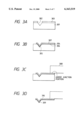
- FIGS. 1A, 1B and 1C show a method of forming a minute aperture in the thus-fabricated cantilever with the metal-coated probe.
- FIGS. 2A and 2B are plan views corresponding to FIGS. 1A and 1C.
- reference numeral 101 designates a probe portion with its sharp tip
- reference numeral 102 designates an elastic cantilever
- reference numeral 103 designates a metal coating.
- a probe portion 108 covered with metal is brought into contact with a metal substrate 105, and a voltage is applied between the probe portion 108 and the metal substrate 105 by a voltage applying unit 106 through an electrode wire 104.
- the coating metal layer at the probe tip portion is removed by electric-field evaporation or thermal melting, thus forming a minute aperture.
- the degree of removal of the coating metal film or the diameter of the minute aperture can be controlled by respectively controlling (1) a diameter of the probe tip, (2) a film thickness of the coating metal 108, (3) a contact force of the probe tip against the metal substrate 105 and (4) a condition of the above applied voltage.
- a contact area of the probe tip against the metal substrate 105 becomes smaller, and the area of applied electric field and the area of current flow concentrate when the voltage is applied.
- the area, where the coating metal film is removed decreases.
- a forming method and metal material which makes it possible to form a rough metal surface when the coating metal film is formed, can be selected, other than a method of sharpening the probe itself by the sharpening treatment.
- low-temperature thermal oxidation is performed after the pyramid-shaped groove is formed by anisotropic etching and thus the tip or bottom of the pyramid-shaped groove can be sharpened.
- Pt film when the sputtering method rather than the evaporation method is selected, Pt grains for forming the Pt film become fine and thus the coated probe tip can be sharpened.
- the area of applied electric field and the area of current flow concentrate when the voltage is applied, similar to the case where the diameter of the probe tip is small. Thus, the area where the coating metal film is removed, decreases.
- the film thickness of the metal film becomes less than 100 nm, there is a tendency that a continuous film is hard to attain. If so, the film is unsuitable for the probe of this invention, and hence it is desirable that the thickness of the metal film is approximately 100 nm.
- the contact force of the metal-coated probe portion 108 against the metal substrate 105 can be controlled to be set to a desired value by elastically deforming the elastic cantilever 102.
- the contact force can be below k ⁇ z by decreasing the amount of the elastic deformation of the elastic cantilever 102 (this is a reduced value relative to the position of the probe portion) due to its contact against the metal substrate 105 to below ⁇ z.
- magnitudes and changes with time of the electric field applied to the probe tip and the current flowing between the probe and the metal substrate can be controlled by adjusting crest value, waveform, time width and load resistance of the applied voltage.
- the degree of removal of the coating metal film can be controlled.
- the diameter of the minute aperture was about 10 nm when the voltage with the crest value of 10 V, square waveform, time width of 100 ⁇ s and load resistance of 1 M ⁇ was applied.
- the diameter of the minute aperture could be controlled in a range between 3 nm and 1000 nm when (1) the diameter of the probe tip, (2) the film thickness of the coating metal, (3) the contact force of the probe tip against the metal substrate and (4) the condition of the applied voltage were changed.
- the aperture with the diameter of above 100 nm the shape of the aperture is likely to be unstable and the probe tip is likely to be broken, maybe for the reason that formation conditions, such as the voltage application condition, the contact force condition and the like, are excessive. Therefore, such a probe is less preferred as the probe of the present invention.
- the range, in which the aperture can be stably formed was a range between about 10 nm and about 100 nm.
- the coating metal of the probe with the thus-formed minute aperture is removed from the probe tip, so the probe tip is not conductive.
- a portion close to the probe tip only needs to be coated with transparent conductive material, such as ITO, by the sputtering method or the like, as illustrated in FIG. 4.
- transparent conductive material such as ITO
- a monomolecular built-up film of conductive material such as polydiacetylene, may be formed on the portion close to the probe tip by Langmuir-Blodgett's technique.
- the above method of forming the probe with the minute aperture can be particularly suitably utilized as a method for simultaneously forming minute apertures in a plurality of probes.
- probe tips of a plurality of probes 502, 503 and 504 are brought into contact with a metal substrate 501, and a voltage is applied between the plural probes and the metal substrate using a voltage applying unit 505.
- a plurality of apertures can be simultaneously formed.
- the plural probes are respectively constructed using elastic cantilevers, even if positional variation in the z-direction in FIG. 5 of the probe tip relative to the metal substrate surface exists due to errors during the fabrication process of the plural probes and the like, the following state can be established: In this state, all the probe tips are in contact with the surface of the metal substrate under the condition under which magnitudes of the contact forces between the probe tips and the metal substrate are below a certain value.
- a demultiplexer In a method of applying the voltage, a demultiplexer can be used. In this case, the voltage is applied to the plural probes in turn and the minute apertures are successively formed in the plural probes. In this case, however, it takes considerable time to form the minute apertures. To solve this disadvantage, it is desirable to apply the voltage while the metal substrate 501 and the support member 506 for the plural probes are moved relative to the metal substrate in a plane parallel to the metal substrate surface. Thereby, the following fear can be prevented: The coating metal material removed from the probe tip during the fabrication of the aperture in a part of the probes can be prevented from being caught between the probe tip and the metal material, and a conductive state or a low-resistance state is created between the probe tip and the metal substrate. As a result, the value of the applied voltage in other probes is lowered, and the minute apertures cannot be formed.
- FIG. 6 illustrates an example of a multiple SNOM using a plurality of probes of the present invention.
- reference numerals 601, 602 and 603 designate SNOM probes 1, 2 and 3 using the probe of this invention, respectively.
- the plural SNOM probes 1, 2 and 3 are integrated with a probe support member 604.
- the design and structure are constructed such that the positions of the photodiodes 1-3 (605-607) are at the back (in FIG. 6, above) of corresponding minute apertures of the SNOM probes 1-3 (601-603).
- the probe of this invention since there is no metal coating at a place opposite to the minute aperture of the probe, an opening having a diameter (about several microns) larger than the minute aperture exists at the back of the minute aperture (see FIGS. 1A to 1C). Therefore, there appears a space at the back of the minute aperture, and the light detecting mechanism, such as the photodiode, can be disposed close to the probe without using a light waveguide or the like. Hence, the probe can be integrated with a light detecting mechanism which does not reduce the light detection resolution.
- An object 609 to be measured is put on a transparent substrate 610.
- Light 611 is input into the object 609 through the transparent substrate 610 from the back side of the object 609 at an angle which satisfies the total reflection condition on the surface of the object 609. At this time, though the light is not transmitted through the surface of the object 609 and does not emerge upward (in FIG. 6), evanescent light issues from the surface of the object 609 within the distance of less than 0.1 ⁇ m from its surface.
- the evanescent light 1 (612), 2 (613) and 3 (614) pass through the minute apertures of the SNOM probes and is detected by the photodiodes 1-3 (605-607) located at the back of the minute apertures.
- Current signals of the detected evanescent light are converted into voltage signals by I/V conversion circuits 1 (615), 2 (616) and 3 (617), and a multiple SNOM signal is created therefrom by a multiplexer 618.
- the following state can be established: In this state, all the probe tips are in contact with the surface of the object under the condition under which magnitudes of the contact forces between the probe tips and the object are below a certain value.
- FIG. 6 an xy actuator (not shown) is used, the object 609 is moved relatively to the plural SNOM probes 1-3 in directions (x- and y-directions in FIG. 6) on the object surface in a two-dimensional relative scanning manner, and magnitudes of the SNOM signals at respective positions in the xy plane are plotted.
- the SNOM observation image of the surface of the object 609 can be obtained.
- FIG. 7 illustrates an example of a multiple SNOM/STM using the conductive probes of the present invention.
- reference numerals 701-703 respectively designate conductive SNOM probes 1-3.
- Reference numeral 704 designates a support member for the probes.
- Reference numerals 705-707 respectively designate photodiodes 1-3.
- Reference numeral 708 designates a support member for the photodiodes.
- Reference numeral 709 designates an object.
- Reference numeral 710 designates a transparent substrate.
- Reference numeral 711 designates light.
- Reference numerals 712-714 designate evanescent light 1-3.
- Reference numerals 715-717 respectively designate I/V conversion circuits 1-3.
- Reference numeral 718 designates a multiplexer 1.
- This example differs from the example of FIG. 6 in that a transparent electrode 719 made of transparent conductive material, such as ITO, is formed on the transparent substrate 710 and the object 709 is put on the transparent electrode 719.
- the transparent electrode 719 is connected to a bias voltage applying unit 720, and a bias voltage is applied to the electrode.
- FIG. 8 illustrates an example of a recording/reproducing apparatus using a plurality of probes of the present invention.
- reference numerals 801, 802 and 803 designate recording and reproducing probes 1, 2 and 3 using the conductive probe of this invention, respectively.
- the plural recording and reproducing probes 1, 2 and 3 are integrated with a probe support member 804.
- the design and structure are constructed such that the positions of the photodiodes 1-3 (805-807) are at the back (in FIG. 8, above) of corresponding minute apertures of the recording and reproducing probes 1-3 (801-803).
- a record medium 809 is put on a transparent electrode 819 on a transparent substrate 810.
- the probe tips of the plural recording and reproducing probes 1-3 (801-803) are so positioned as to be in contact with the surface of the record medium 809.
- a voltage signal of information to be recorded is divided by a demultiplexer 820, and the divided ones are applied to the conductive probes of the respective recording and reproducing probes 1-3 (801-803).
- the recording is performed on a local portion of the record medium 809 with which the conductive probe is in contact.
- the record medium 809 is made of material whose optical characteristic is changed by the application of a voltage or electric-field, or injection of current (described below).
- Light 811 is input into the record medium 809 through the transparent substrate 810 from the back side of the record medium 809 at an angle which satisfies the total reflection condition on the surface of the record medium 809. At this time, though the light is not transmitted through the surface of the record medium 809 and does not emerge upward (in FIG. 8), the evanescent light escaped from the surface of the record medium 809 within a distance of less than 0.1 ⁇ m from its surface.
- the evanescent light 1 (812), 2 (813) and 3 (814) passes through the minute apertures of the recording and reproducing probes and is detected by the photodiodes 1-3 (805-807) located at the back of the minute apertures.
- Current signals of the detected evanescent light are converted into voltage signals by I/V conversion circuits 1 (815), 2 (816) and 3 (817), and those voltage signals are combined by a multiplexer 818.
- a reproduced signal is created therefrom.
- the following state can be established: In this state, all the probe tips are in contact with the surface of the record medium under the condition under which magnitudes of the contact forces between the probe tips and the record medium are below a certain value.
- an xy actuator (not shown) is used, the record medium 809 is moved relative to the plural recording and reproducing probes 1-3 in directions (x- and y-directions in FIG. 8) on the record medium surface in a two-dimensional relative scanning manner, and recording and reproduction are executed at predetermined locations in the xy plane.
- the recording and reproduction are conducted using the plural recording and reproducing probes with the minute apertures, the recording and reproduction can be performed to the record medium with a high density and at high speed.
- the recording is performed by the application of the voltage in this embodiment, but it is possible in the structure of this embodiment to apply a voltage under a condition under which light is illuminated.
- the record medium is a medium to which the recording is conducted by applying a voltage under the light-illuminated condition.
- the following record media can be used.
- the record medium whose optical characteristic is changed by the voltage application there exists a medium of 10, 12-pentacosadiynoic acid disclosed in Japanese Patent Application Laid-Open No. 4-90152, in which the voltage application causes a structural change in diacetylene derivative polymer due to Joule heat created by locally-flowing current and the peak wavelength of light absorption band is hence shifted.
- the forming method is simple and no complicated steps are needed, so the processing time for forming the minute aperture is short and the minute aperture can be formed with a small variation and with good yield. Further, its cost can be reduced and the probe can be readily integrated and made compact in size.
- the minute aperture forming method of the probe fabrication method according to the present invention in which the metal-coated probe is brought into contact with metal material and the coating metal at the probe tip is removed by the voltage application, since the minute aperture with the diameter of about 10 nm can be formed, it is possible to improve the measurement resolution and reproduction precision by using the probe with this minute aperture in the SNOM or recording and/or reproducing apparatus.
- the probe fabrication method of the present invention is a method suitable for the down-sizing and integration, it is possible to readily obtain a compact SNOM or recording and/or reproducing apparatus and a compact SNOM or recording and/or reproducing apparatus having a plurality of optical probes by using that probe fabrication method of the present invention.
- the probe of the present invention no conductive coating thin film is formed at an opposite side of the probe opposed to the surface of the probe tip with the minute aperture, so that a space can be provided at the back of the minute aperture and the light detecting mechanism, such as the photodiode, can be arranged without any difficulty.
- the probe can be integrated with the light detecting mechanism without reducing the light detecting resolution.
Abstract
In a method of manufacturing a probe with a minute aperture, the probe is coated with conductive material, a tip of the probe is brought into contact with a conductive substrate and a voltage is applied between the probe and the substrate to remove the coating material at the tip of the probe and form the minute aperture at the tip of the probe. The thus-fabricated probe can be used in a scanning near-field optical microscope for observing an object on the basis of a change in intensity of near-field light and an information recording and/or reproducing apparatus for reproducing information recorded in a record medium by using near-field light.
Description
This is a divisional application of application Ser. No. 08/825,129, filed Dec. 20, 1999, now U.S. Pat. No. 6,046,972.
1. Field of the Invention
The present invention relates to a method of manufacturing or producing a probe with a minute aperture suitable for use in a scanning near-field optical microscope, an information recording and/or reproducing apparatus using the principle of that scanning near-field optical microscope and the like, a scanning near-field optical microscope using that probe and a recording and/or reproducing apparatus using that probe.
2. Related Background Art
In recent years, a scanning tunneling microscope (hereinafter referred to as STM) has been developed to make it possible to observe the surface of conductive material with the sub-nanometer resolution (see U.S. Pat. No. 4,343,993). Thus, the arrangement of atoms on the surface of metal, semiconductor or the like, orientation of organic molecules and the like can be observed on an atomic or molecular scale.
Further, the STM technology has been expanded, and an atomic force microscope (hereinafter referred to as AFM) has been developed to make it possible to observe the surface of an insulating material or the like with a resolution similar to that of the STM (see U.S. Pat. No. 4,724,318).
Further, as the developed STM, a scanning near-field optical microscope (hereinafter referred to as SNOM) has been proposed to examine the surface condition of an object by using evanescent light issuing from a minute aperture formed at a sharp tip of a probe (see Durig, et al, J. Appl. Phys. 59, 3318 (1986)).
Furthermore, a photon STM (hereinafter referred to as PSTM) has been also developed, which is a kind of SNOM for examining the surface of an object by inputting light into the object from its bottom surface through a prism under the condition of total reflection and detecting evanescent light, which exudes toward the object surface, by an optical probe from the side of the object surface (see Reddick, et al, Phys. Rev. B39, 767 (1989)).
In the above SNOM, various kinds of methods for fabricating an optical probe have been devised so far since the resolution is determined by the tip diameter of the optical probe. For example, in order to increase the resolution, no minute aperture is formed at the tip of the optical probe in the PSTM and instead the tip of an optical fiber, which is used as the optical probe, is sharpened by optimizing chemical etching conditions on the end surface of the optical fiber.
Further, at the initial stage of manufacturing an SNOM, the intersection portion between cleaved surfaces of transparent crystal is coated with metal, the metal at the intersection portion is pushed against a hard face and removed therefrom and thus the pushed intersection portion is exposed to form a minute aperture (see European Patent No. 0112402). More recently, a method for forming a minute aperture by using a lithographic method has been also used.
Furthermore, a method for fabricating an optical probe by constructing integrate minute aperture and light waveguide has been proposed (see U.S. Pat. No. 5,354,985).
However, in the above conventional technologies, where no minute aperture is formed in the optical probe as in the PSTM, stray light other than the evanescent light, such as light scattering generated due to an uneven portion of the object surface, is undesirably detected and the resolution is likely to be lowered.
Further, in the method in which the optical fiber is etched, it is difficult to fabricate an integrated and compact optical probe.
In the conventional method of forming the minute aperture in which the cleaved surfaces of the crystal is used, the size of the diameter of the minute aperture is apt to vary and its yield is not good. In addition, integration and compact construction are hard to attain.
Further, in the conventional method of forming the minute aperture using the photolithography, the limit in the diameter of the aperture is about 100 nm due to the limitation in precision of its processing apparatus, and thus it is difficult to fabricate the minute aperture with a diameter of about 10 nm. Hence, there is a limitation of the resolution of the SNOM apparatus. Furthermore, the processing is apt to be complicated, considerable time is required and its cost is relatively high.
If EB (electron beam) processing apparatus or FIB (focused ion beam) processing apparatus is used, it is in principle possible to form an aperture of less than 100 nm. However, the positional alignment control is complicated and variation is likely to occur. Further, yield is not good since the processing is performed point by point.
Therefore, in order to solve the above problems of the above-discussed conventional technologies, it is an object of the present invention to provide a method of fabricating a probe having a minute aperture with a reduced variation in its size, according to which the minute aperture can be readily formed in a short time with good yield, an integrate and compact structure can be achieved and the resolution is improved, a probe formed by this method, a composite apparatus of scanning near-field optical microscope and scanning tunneling microscope using this probe and a recording and/reproducing apparatus using this probe.
In order to achieve the above object, there is provided a method of fabricating a probe with a minute aperture, which includes the steps of:
coating the probe with conductive material; and
bringing a tip of the probe into contact with a conductive substrate and applying a voltage between the probe and the substrate to remove the coating material at the tip of the probe and form the minute aperture at the tip of the probe.
Further, in order to achieve the above object, there is provided a scanning near-field optical microscope for observing an object on the basis of a change in intensity of near-field light, which includes:
a probe having a minute aperture at its tip;
a unit for moving the probe relatively to the object;
a unit for illuminating the object with light; and
a photodetector arranged at the back of the minute aperture to detect the intensity of the near-field light created by the light illumination and passing through the minute aperture.
Further, in order to achieve the above object, there is provided an information recording and/or reproducing apparatus for reproducing information recorded in a record medium by using near-field light, which includes:
a probe having a minute aperture at its tip;
a unit for moving the probe relatively to the record medium;
a unit for illuminating the record medium with light;
a photodetector arranged at the back of the minute aperture to detect the intensity of the near-field light created by the light illumination and passing through the minute aperture; and
a unit for reproducing the information on the basis of the detected light intensity.
The above and other objects and features of the present invention will become apparent from the following description.
FIGS. 1A, 1B and 1C are respectively cross-sectional views showing a method of the present invention for forming a minute aperture;
FIGS. 2A and 2B are respectively views showing the method of the present invention for forming the minute aperture, and FIG. 2A is a plan view of FIG. 1A and FIG. 2B is a plan view of FIG. 1C;
FIGS. 3A, 3B, 3C and 3D are respectively cross-sectional views showing a method of the present invention for fabricating an elastic cantilever having a probe tip coated with metal;
FIG. 4 is a cross-sectional view showing the structure of a probe having a conductive probe tip;
FIG. 5 is a sectional view showing a method for simultaneously fabricating a plurality of minute apertures in a plurality of probes;
FIG. 6 is a view showing the structure of a multiple SNOM using a plurality of probes of the present invention;
FIG. 7 is a view showing the structure of a multiple SNOM/STM using the conductive probe of the present invention; and
FIG. 8 is a view showing the structure of a recording and/or reproducing apparatus using a plurality of probes of the present invention.
The preferred embodiments of the present invention will be described in detail below with reference to the accompanying drawings.
According to the present invention, there can be provided a method of fabricating a probe having a minute aperture with a reduced variation according to which the minute aperture can be readily formed in a short time with good yield, an integrate and compact structure can be achieved with improved resolution, and a probe formed by this method. Further, a composite apparatus of scanning near-field optical microscope and scanning tunneling microscope using the thus-produced probe can be constructed, and a measurement resolution can be improved. Furthermore, a recording and/reproducing apparatus using this probe can be constructed, and a reproduction accuracy can be enhanced. In addition, a multiple structure can be built by a plurality of the probes, and hence high-speed recording and/or reproduction of a large capacity of data can be achieved.
Embodiments of the present invention will be described hereinafter with reference to the drawings.
FIGS. 1A, 1B, 1C, 2A, 2B, 3A, 3B, 3C and 3D illustrate a fabrication method of a probe with a minute aperture according to the present invention. Initially, regarding the fabrication method of the probe, a fabrication method of an elastic cantilever with a probe having a tip portion coated with metal will be described with reference to FIGS. 3A to 3D.
As illustrated in FIG. 3A, an SiO2 mask 303 is deposited on an Si substrate 301 having a face orientation (100), except for a square portion of 5μ×5μ, and anisotropic etching is performed using a potassium hydroxide (KOH) solution, by which means a pyramid-shaped recess or groove 302 is formed.
Then, after a Pt (platinum) layer 304 having a thickness of 0.1 μm is formed by a sputtering method as illustrated in FIG. 3B, and the patterning of a probe-tip coat portion 305 and an electrode wiring 306 is performed. After that, an Si3 N4 layer 307 having a thickness of 1 μm is formed by a low pressure chemical vapour deposition (LP-CVD), and then the patterning of a cantilever shape is conducted.
Further, a glass substrate 308 is anode-joined (see an anode junction portion) to support the cantilever, as illustrated in FIG. 3C. Finally, as illustrated in FIG. 3D, the Si substrate 301 is removed by a KOH solution, and thus an elastic cantilever 310 having a probe tip 309 coated with Pt is formed.
FIGS. 1A, 1B and 1C show a method of forming a minute aperture in the thus-fabricated cantilever with the metal-coated probe. FIGS. 2A and 2B are plan views corresponding to FIGS. 1A and 1C.
In FIGS. 1A and 2A, reference numeral 101 designates a probe portion with its sharp tip, reference numeral 102 designates an elastic cantilever and reference numeral 103 designates a metal coating. A probe portion 108 covered with metal is brought into contact with a metal substrate 105, and a voltage is applied between the probe portion 108 and the metal substrate 105 by a voltage applying unit 106 through an electrode wire 104. The coating metal layer at the probe tip portion is removed by electric-field evaporation or thermal melting, thus forming a minute aperture.
Here, the degree of removal of the coating metal film or the diameter of the minute aperture can be controlled by respectively controlling (1) a diameter of the probe tip, (2) a film thickness of the coating metal 108, (3) a contact force of the probe tip against the metal substrate 105 and (4) a condition of the above applied voltage. As the probe tip diameter decreases, a contact area of the probe tip against the metal substrate 105 becomes smaller, and the area of applied electric field and the area of current flow concentrate when the voltage is applied. Thus, the area, where the coating metal film is removed, decreases.
In order to reduce the probe tip diameter, a forming method and metal material, which makes it possible to form a rough metal surface when the coating metal film is formed, can be selected, other than a method of sharpening the probe itself by the sharpening treatment.
In an example in the above-discussed forming method of the elastic cantilever, low-temperature thermal oxidation is performed after the pyramid-shaped groove is formed by anisotropic etching and thus the tip or bottom of the pyramid-shaped groove can be sharpened. Further, where the Pt film is formed, when the sputtering method rather than the evaporation method is selected, Pt grains for forming the Pt film become fine and thus the coated probe tip can be sharpened.
When the film thickness of the coating metal film is small, the area of applied electric field and the area of current flow concentrate when the voltage is applied, similar to the case where the diameter of the probe tip is small. Thus, the area where the coating metal film is removed, decreases.
However, though depending on the forming method, if the film thickness of the metal film becomes less than 100 nm, there is a tendency that a continuous film is hard to attain. If so, the film is unsuitable for the probe of this invention, and hence it is desirable that the thickness of the metal film is approximately 100 nm.
Further, as the contact force decreases, the contact area of the probe tip against the metal substrate decreases and thus the area, where the coating metal film is removed, also becomes small. The following method may be taken to reduce the contact force. The contact force of the metal-coated probe portion 108 against the metal substrate 105 can be controlled to be set to a desired value by elastically deforming the elastic cantilever 102. For example, when the elastic constant with respect to the elastic deformation of the elastic cantilever 102 (this is a reduced value relative to the position of the probe portion) is indicated by k, the contact force can be below kΔz by decreasing the amount of the elastic deformation of the elastic cantilever 102 (this is a reduced value relative to the position of the probe portion) due to its contact against the metal substrate 105 to below Δz. Further, magnitudes and changes with time of the electric field applied to the probe tip and the current flowing between the probe and the metal substrate can be controlled by adjusting crest value, waveform, time width and load resistance of the applied voltage. Thus, the degree of removal of the coating metal film can be controlled.
Actually, in the case where the probe with the metal coating material of Pt and the tip diameter of 20 nm is prepared and the elastic cantilever is brought into contact with a metal substrate of Au under the condition under which the amount of elastic deformation of the elastic cantilever with its elastic constant of 0.1 N/m is set to less than 1 μm, i.e., the contact force is set to less than 10-7 N, the diameter of the minute aperture was about 10 nm when the voltage with the crest value of 10 V, square waveform, time width of 100 μs and load resistance of 1 MΩ was applied.
In the method of forming the minute aperture of the present invention, the diameter of the minute aperture could be controlled in a range between 3 nm and 1000 nm when (1) the diameter of the probe tip, (2) the film thickness of the coating metal, (3) the contact force of the probe tip against the metal substrate and (4) the condition of the applied voltage were changed. However, in a case where the aperture with the diameter of above 100 nm is formed, the shape of the aperture is likely to be unstable and the probe tip is likely to be broken, maybe for the reason that formation conditions, such as the voltage application condition, the contact force condition and the like, are excessive. Therefore, such a probe is less preferred as the probe of the present invention. Further, where the aperture is less than 10 nm, its reproducible property is not good. Therefore, the range, in which the aperture can be stably formed, was a range between about 10 nm and about 100 nm.
The coating metal of the probe with the thus-formed minute aperture is removed from the probe tip, so the probe tip is not conductive.
Therefore, in the case where the prove is used in an apparatus which requires the electric conductivity of the probe tip, a portion close to the probe tip only needs to be coated with transparent conductive material, such as ITO, by the sputtering method or the like, as illustrated in FIG. 4. Alternatively, a monomolecular built-up film of conductive material, such as polydiacetylene, may be formed on the portion close to the probe tip by Langmuir-Blodgett's technique.
The above method of forming the probe with the minute aperture can be particularly suitably utilized as a method for simultaneously forming minute apertures in a plurality of probes. As illustrated in FIG. 5, probe tips of a plurality of probes 502, 503 and 504 are brought into contact with a metal substrate 501, and a voltage is applied between the plural probes and the metal substrate using a voltage applying unit 505. Thus, a plurality of apertures can be simultaneously formed.
Since the plural probes are respectively constructed using elastic cantilevers, even if positional variation in the z-direction in FIG. 5 of the probe tip relative to the metal substrate surface exists due to errors during the fabrication process of the plural probes and the like, the following state can be established: In this state, all the probe tips are in contact with the surface of the metal substrate under the condition under which magnitudes of the contact forces between the probe tips and the metal substrate are below a certain value. For example, where k is the elastic constant of the elastic cantilever and Δz' is the maximum value of the positional variation in the z-direction of the probe tip relative to the metal substrate surface occurring due to errors during the fabrication process of the plural probes and the like, since the variation in the contact force in the state, in which all the probe tips are brought into contact with the surface of the metal substrate, is kΔz', magnitudes of all the contact forces can be below kΔz' in the state in which all the probe tips are in contact with the surface of the metal substrate, by controlling the positions in the z-direction of a support member 506 for the plural probe tips and the substrate 501.
In a method of applying the voltage, a demultiplexer can be used. In this case, the voltage is applied to the plural probes in turn and the minute apertures are successively formed in the plural probes. In this case, however, it takes considerable time to form the minute apertures. To solve this disadvantage, it is desirable to apply the voltage while the metal substrate 501 and the support member 506 for the plural probes are moved relative to the metal substrate in a plane parallel to the metal substrate surface. Thereby, the following fear can be prevented: The coating metal material removed from the probe tip during the fabrication of the aperture in a part of the probes can be prevented from being caught between the probe tip and the metal material, and a conductive state or a low-resistance state is created between the probe tip and the metal substrate. As a result, the value of the applied voltage in other probes is lowered, and the minute apertures cannot be formed.
Since the above disadvantage (catching of the removed material) is removed in this method, minute apertures are simultaneously formed in the plural probes without fail.
Now, the application of the thus-fabricated probe will be described. FIG. 6 illustrates an example of a multiple SNOM using a plurality of probes of the present invention. In FIG. 6, reference numerals 601, 602 and 603 designate SNOM probes 1, 2 and 3 using the probe of this invention, respectively. The plural SNOM probes 1, 2 and 3 are integrated with a probe support member 604. Further, a photodiode support member 608, on which a plurality of high-sensitivity photodiodes 1 (605), 2 (606) and 3 (607), such as avalanche photodiodes, are mounted, is fixed to and integrated with the probe support member 604. The design and structure are constructed such that the positions of the photodiodes 1-3 (605-607) are at the back (in FIG. 6, above) of corresponding minute apertures of the SNOM probes 1-3 (601-603).
In the probe of this invention, since there is no metal coating at a place opposite to the minute aperture of the probe, an opening having a diameter (about several microns) larger than the minute aperture exists at the back of the minute aperture (see FIGS. 1A to 1C). Therefore, there appears a space at the back of the minute aperture, and the light detecting mechanism, such as the photodiode, can be disposed close to the probe without using a light waveguide or the like. Hence, the probe can be integrated with a light detecting mechanism which does not reduce the light detection resolution. An object 609 to be measured is put on a transparent substrate 610. Light 611 is input into the object 609 through the transparent substrate 610 from the back side of the object 609 at an angle which satisfies the total reflection condition on the surface of the object 609. At this time, though the light is not transmitted through the surface of the object 609 and does not emerge upward (in FIG. 6), evanescent light issues from the surface of the object 609 within the distance of less than 0.1 μm from its surface. At this time, when the probe tips of the plural SNOM probes 1-3 (601-603) are so positioned as to be in contact with the object, the evanescent light 1 (612), 2 (613) and 3 (614) pass through the minute apertures of the SNOM probes and is detected by the photodiodes 1-3 (605-607) located at the back of the minute apertures. Current signals of the detected evanescent light are converted into voltage signals by I/V conversion circuits 1 (615), 2 (616) and 3 (617), and a multiple SNOM signal is created therefrom by a multiplexer 618.
Since the plural SNOM probes are respectively elastic cantilevers, the following state can be established: In this state, all the probe tips are in contact with the surface of the object under the condition under which magnitudes of the contact forces between the probe tips and the object are below a certain value. For example, where k is the elastic constant of the elastic cantilever and Δz" is the maximum value of the positional variation in the z-direction of the probe tip relative to the object surface occurring due to errors during the fabrication process of the plural SNOM probes and the like, since the variation in the contact force in the state, in which all the probe tips are brought into contact with the surface of the object, is kΔz", magnitudes of all the contact forces can be below kΔz" by controlling the positions in the z-direction of the probe support member 604 and the object 609.
Thereby, damage to the probe tips and the object due to large contact forces can be prevented. In FIG. 6, an xy actuator (not shown) is used, the object 609 is moved relatively to the plural SNOM probes 1-3 in directions (x- and y-directions in FIG. 6) on the object surface in a two-dimensional relative scanning manner, and magnitudes of the SNOM signals at respective positions in the xy plane are plotted. Thus, the SNOM observation image of the surface of the object 609 can be obtained.
FIG. 7 illustrates an example of a multiple SNOM/STM using the conductive probes of the present invention.
In FIG. 7, reference numerals 701-703 respectively designate conductive SNOM probes 1-3. Reference numeral 704 designates a support member for the probes. Reference numerals 705-707 respectively designate photodiodes 1-3. Reference numeral 708 designates a support member for the photodiodes. Reference numeral 709 designates an object. Reference numeral 710 designates a transparent substrate. Reference numeral 711 designates light. Reference numerals 712-714 designate evanescent light 1-3. Reference numerals 715-717 respectively designate I/V conversion circuits 1-3. Reference numeral 718 designates a multiplexer 1.
The structure, functions and operations of those structures are the same as those described with reference to FIG. 6. This example differs from the example of FIG. 6 in that a transparent electrode 719 made of transparent conductive material, such as ITO, is formed on the transparent substrate 710 and the object 709 is put on the transparent electrode 719. The transparent electrode 719 is connected to a bias voltage applying unit 720, and a bias voltage is applied to the electrode. Currents flowing between the probe tips of the conductive SNOM probes 1-3 (701-703) and the transparent electrode 719, i.e., currents flowing through a portion of the object in contact with the probe tips are converted into voltage signals by I/V conversion circuits 1' (721), 2' (722) and 3' (723), and a multiple STM signal is created therefrom by a multiplexer 2 (724). Together with the SNOM signal, magnitudes of the STM signals at respective positions in the xy plane during the two-dimensional relative scanning are plotted, and hence the SNOM/STM simultaneous observation image of the surface of the object 709 can be obtained.
Next, FIG. 8 illustrates an example of a recording/reproducing apparatus using a plurality of probes of the present invention. In FIG. 8, reference numerals 801, 802 and 803 designate recording and reproducing probes 1, 2 and 3 using the conductive probe of this invention, respectively. The plural recording and reproducing probes 1, 2 and 3 are integrated with a probe support member 804. Further, a photodiode support member 808, on which a plurality of high-sensitivity photodiodes 1 (805), 2 (806) and 3 (807), such as avalanche photodiodes, are mounted, is fixed to and integrated with the probe support member 804. The design and structure are constructed such that the positions of the photodiodes 1-3 (805-807) are at the back (in FIG. 8, above) of corresponding minute apertures of the recording and reproducing probes 1-3 (801-803).
A record medium 809 is put on a transparent electrode 819 on a transparent substrate 810. The probe tips of the plural recording and reproducing probes 1-3 (801-803) are so positioned as to be in contact with the surface of the record medium 809.
A voltage signal of information to be recorded is divided by a demultiplexer 820, and the divided ones are applied to the conductive probes of the respective recording and reproducing probes 1-3 (801-803). The recording is performed on a local portion of the record medium 809 with which the conductive probe is in contact. The record medium 809 is made of material whose optical characteristic is changed by the application of a voltage or electric-field, or injection of current (described below).
A reproducing method of reproducing the thus-recorded information will be described. Light 811 is input into the record medium 809 through the transparent substrate 810 from the back side of the record medium 809 at an angle which satisfies the total reflection condition on the surface of the record medium 809. At this time, though the light is not transmitted through the surface of the record medium 809 and does not emerge upward (in FIG. 8), the evanescent light escaped from the surface of the record medium 809 within a distance of less than 0.1 μm from its surface. At this time, the evanescent light 1 (812), 2 (813) and 3 (814) passes through the minute apertures of the recording and reproducing probes and is detected by the photodiodes 1-3 (805-807) located at the back of the minute apertures. Current signals of the detected evanescent light are converted into voltage signals by I/V conversion circuits 1 (815), 2 (816) and 3 (817), and those voltage signals are combined by a multiplexer 818. Thus, a reproduced signal is created therefrom.
Since the plural recording and reproducing probes are respectively constructed by elastic cantilevers, the following state can be established: In this state, all the probe tips are in contact with the surface of the record medium under the condition under which magnitudes of the contact forces between the probe tips and the record medium are below a certain value. For example, where k is the elastic constant of the elastic cantilever and Δz" is the maximum value of the positional variation in the z-direction of the probe tip relative to the record medium surface occurring due to errors during the fabrication process of the plural recording and reproducing probes and the like, since the variation in the contact force in the state, in which all the probe tips are brought into contact with the surface of the record medium, is kΔz", magnitudes of all the contact forces can be below kΔz" by controlling the positions in the z-direction of the probe support member 804 and the record medium 809.
Thereby, damage to the probe tips and the record medium due to large contact forces can be prevented.
In FIG. 6, an xy actuator (not shown) is used, the record medium 809 is moved relative to the plural recording and reproducing probes 1-3 in directions (x- and y-directions in FIG. 8) on the record medium surface in a two-dimensional relative scanning manner, and recording and reproduction are executed at predetermined locations in the xy plane.
In this embodiment, since the recording and reproduction are conducted using the plural recording and reproducing probes with the minute apertures, the recording and reproduction can be performed to the record medium with a high density and at high speed.
Further, the recording is performed by the application of the voltage in this embodiment, but it is possible in the structure of this embodiment to apply a voltage under a condition under which light is illuminated. In such a case, the record medium is a medium to which the recording is conducted by applying a voltage under the light-illuminated condition.
As the record medium to be used in the recording and reproducing apparatus of this embodiment, the following record media can be used. As the record medium whose optical characteristic is changed by the voltage application, there exists a medium of 10, 12-pentacosadiynoic acid disclosed in Japanese Patent Application Laid-Open No. 4-90152, in which the voltage application causes a structural change in diacetylene derivative polymer due to Joule heat created by locally-flowing current and the peak wavelength of light absorption band is hence shifted.
As the record medium whose optical characteristic is changed by the voltage application under the light-illuminated condition, there exists a medium of azo chemical compound having quinone radical and hydroquinone radical disclosed in Japanese Patent Application Laid-Open No. 2-98849, in which photoisomerization reaction between cis-type and trans-type occurs only at the time of light illumination to form redox-pairs and the application of electric-field causes the proton movement between the redox-pairs.
In the above-discussed method of forming the probe according to the present invention, the forming method is simple and no complicated steps are needed, so the processing time for forming the minute aperture is short and the minute aperture can be formed with a small variation and with good yield. Further, its cost can be reduced and the probe can be readily integrated and made compact in size.
Further, in the minute aperture forming method of the probe fabrication method according to the present invention in which the metal-coated probe is brought into contact with metal material and the coating metal at the probe tip is removed by the voltage application, since the minute aperture with the diameter of about 10 nm can be formed, it is possible to improve the measurement resolution and reproduction precision by using the probe with this minute aperture in the SNOM or recording and/or reproducing apparatus.
Further, since the probe fabrication method of the present invention is a method suitable for the down-sizing and integration, it is possible to readily obtain a compact SNOM or recording and/or reproducing apparatus and a compact SNOM or recording and/or reproducing apparatus having a plurality of optical probes by using that probe fabrication method of the present invention.
Further, in the probe of the present invention, no conductive coating thin film is formed at an opposite side of the probe opposed to the surface of the probe tip with the minute aperture, so that a space can be provided at the back of the minute aperture and the light detecting mechanism, such as the photodiode, can be arranged without any difficulty. Thus, the probe can be integrated with the light detecting mechanism without reducing the light detecting resolution.
Claims (4)
1. A scanning near-field optical microscope for observing an object on the basis of a change in intensity of near-field light, said microscope comprising:
a probe having a minute aperture at its tip supported by an elastic member;
means for moving the probe relatively to the object; means for illuminating the object with light;
a photodetector to detect the intensity of the near-field light created by the light illumination and passing through the minute aperture;
first member supporting the elastic member; and
a second member provided with the detector,
wherein said first member and said second member are integrated so that the photodetector is arranged in the back proximity of the minute aperture.
2. A scanning near-field optical microscope according to claim 1, wherein a plurality of said probes are provided on said first member and a plurality of said photodetectors are provided on said second member, said plurality of photodetectors being arranged corresponding to respective positions of said plurality of probes.
3. An information recording and/or reproducing apparatus for reproducing information recorded in a record medium by using near-field light, said apparatus comprising:
a probe having a minute aperture at its tip supported by an elastic member;
means for moving the probe relative to the record medium;
means for illuminating the record medium with light;
a photodetector to detect the intensity of the near-field light created by the light illumination and passing through the minute aperture;
means for reproducing information on the basis of the light intensity detected by the photodetector;
a first member supporting the elastic member; and
a second member provided with the photodetector,
wherein said first member and said second member are integrated so that the photodetector is arranged in the back proximity of the minute aperture.
4. An information recording and/or reproducing apparatus according to claim 3, wherein a plurality of said probes are provided on said first member and a plurality of said photodetectors are provided on said second member, said plurality of photodetectors being arranged corresponding to respective positions of said plurality of probes.
Priority Applications (1)
| Application Number | Priority Date | Filing Date | Title |
|---|---|---|---|
| US09/518,104 US6163519A (en) | 1996-03-29 | 2000-03-03 | Scanning near-field optical microscope using the probe and recording and/or reproducing apparatus using the probe |
Applications Claiming Priority (4)
| Application Number | Priority Date | Filing Date | Title |
|---|---|---|---|
| JP10336196A JP3618896B2 (en) | 1996-03-29 | 1996-03-29 | Manufacturing method of probe having minute aperture, probe thereby, combined apparatus of scanning near-field light microscope and scanning tunneling microscope using the probe, and recording / reproducing apparatus using the probe |
| JP8-103361 | 1996-03-29 | ||
| US08/825,129 US6046972A (en) | 1996-03-29 | 1997-03-27 | Method and producing probe with minute aperture, scanning near-field optical microscope using the probe and recording and/or reproducing apparatus using the probe |
| US09/518,104 US6163519A (en) | 1996-03-29 | 2000-03-03 | Scanning near-field optical microscope using the probe and recording and/or reproducing apparatus using the probe |
Related Parent Applications (1)
| Application Number | Title | Priority Date | Filing Date |
|---|---|---|---|
| US08825129 Division | 1999-12-20 |
Publications (1)
| Publication Number | Publication Date |
|---|---|
| US6163519A true US6163519A (en) | 2000-12-19 |
Family
ID=14351998
Family Applications (2)
| Application Number | Title | Priority Date | Filing Date |
|---|---|---|---|
| US08/825,129 Expired - Fee Related US6046972A (en) | 1996-03-29 | 1997-03-27 | Method and producing probe with minute aperture, scanning near-field optical microscope using the probe and recording and/or reproducing apparatus using the probe |
| US09/518,104 Expired - Fee Related US6163519A (en) | 1996-03-29 | 2000-03-03 | Scanning near-field optical microscope using the probe and recording and/or reproducing apparatus using the probe |
Family Applications Before (1)
| Application Number | Title | Priority Date | Filing Date |
|---|---|---|---|
| US08/825,129 Expired - Fee Related US6046972A (en) | 1996-03-29 | 1997-03-27 | Method and producing probe with minute aperture, scanning near-field optical microscope using the probe and recording and/or reproducing apparatus using the probe |
Country Status (2)
| Country | Link |
|---|---|
| US (2) | US6046972A (en) |
| JP (1) | JP3618896B2 (en) |
Cited By (15)
| Publication number | Priority date | Publication date | Assignee | Title |
|---|---|---|---|---|
| WO2002080187A1 (en) * | 2001-03-29 | 2002-10-10 | Eidgenössische Technische Hochschule Zürich | Array and method for quasi-parallel probe microscopy |
| WO2002080186A1 (en) * | 2001-03-30 | 2002-10-10 | Johns Hopkins University | Afm cantilevers and methods for making and using same |
| US6831765B2 (en) | 2001-02-22 | 2004-12-14 | Canon Kabushiki Kaisha | Tiltable-body apparatus, and method of fabricating the same |
| EP1533804A1 (en) * | 2003-11-21 | 2005-05-25 | Pioneer Corporation | Recording / reproducing head, recording / reproducing head array, method of producing the same, and recording apparatus and reproducing apparatus |
| US20060171728A1 (en) * | 2003-03-28 | 2006-08-03 | Canon Kaushiki Kaisha | Electric potential measuring device using oscillating device, image forming apparatus, and electric potential measuring method |
| US20060188398A1 (en) * | 2003-08-27 | 2006-08-24 | Canon Kabushiki Kaisha | Sensor for detecting a target substance in a fluid |
| US20060267578A1 (en) * | 2005-05-27 | 2006-11-30 | Canon Kabushiki Kaisha | Potential measuring apparatus |
| US20060267593A1 (en) * | 2005-05-16 | 2006-11-30 | Canon Kabushiki Kaisha | Potential measuring device and image forming apparatus using the same |
| US20070041238A1 (en) * | 2005-07-08 | 2007-02-22 | Nanochip, Inc. | High density data storage devices with read/write probes with hollow or reinforced tips |
| DE19926601B4 (en) * | 1998-09-12 | 2007-03-29 | Witec Wissenschaftliche Instrumente Und Technologie Gmbh | Aperture in a semiconductor material and production of the aperture and use |
| US20070182419A1 (en) * | 2006-02-09 | 2007-08-09 | Canon Kabushiki Kaisha | Oscillating device, electric potential measuring device, light deflecting device, and image forming apparatus |
| US20080144029A1 (en) * | 2006-11-30 | 2008-06-19 | Chian Chiu Li | Near-Field Optical Apparatus And Method Using Photodetector Array |
| US20090168636A1 (en) * | 2007-12-31 | 2009-07-02 | Tsung-Kuan Allen Chou | Cantilever design with electrostatic-force-modulated piezoresponse force microscopy (pfm) sensing |
| US20130332100A1 (en) * | 2010-11-24 | 2013-12-12 | Christopher David Young | Mechanical testing instruments including onboard data |
| CN104237568A (en) * | 2014-09-16 | 2014-12-24 | 上海应用技术学院 | Scanning near-field optical microscope active integrated probe and manufacturing method thereof |
Families Citing this family (26)
| Publication number | Priority date | Publication date | Assignee | Title |
|---|---|---|---|---|
| US6806477B1 (en) | 1997-05-23 | 2004-10-19 | Canon Kabushiki Kaisha | Position detection device, apparatus using the same, exposure apparatus, and device manufacturing method using the same |
| JP3697034B2 (en) * | 1997-08-26 | 2005-09-21 | キヤノン株式会社 | Method of manufacturing protrusions having minute openings, and probes or multiprobes using them |
| JPH11166935A (en) * | 1997-09-25 | 1999-06-22 | Canon Inc | Light probe for light detection or irradiation, near-field optical microscope provided with the probe, manufacture of the light probe and substrate used for its manufacture |
| JP3862845B2 (en) * | 1998-02-05 | 2006-12-27 | セイコーインスツル株式会社 | Near-field optical probe |
| JP4145985B2 (en) * | 1998-02-10 | 2008-09-03 | セイコーインスツル株式会社 | Information recording device |
| JP4083330B2 (en) * | 1998-02-25 | 2008-04-30 | セイコーインスツル株式会社 | Near-field optical memory head |
| JP4020229B2 (en) * | 1998-05-11 | 2007-12-12 | セイコーインスツル株式会社 | Near-field optical head |
| IL124838A0 (en) * | 1998-06-10 | 1999-01-26 | Yeda Res & Dev | Near-field optical inspection apparatus |
| JP2000035396A (en) * | 1998-07-16 | 2000-02-02 | Canon Inc | Probe with minute protrusion and its manufacturing method |
| JP3554233B2 (en) | 1998-10-28 | 2004-08-18 | キヤノン株式会社 | Optical probe manufacturing method |
| CN1275248C (en) | 1999-05-31 | 2006-09-13 | 富士通株式会社 | Recording head, method of manufacturing recording head, information recording device |
| JP4472863B2 (en) | 1999-12-20 | 2010-06-02 | セイコーインスツル株式会社 | Near-field optical probe and near-field optical device using the near-field optical probe |
| JP2002116131A (en) * | 2000-08-03 | 2002-04-19 | National Institute Of Advanced Industrial & Technology | Near-field probe and its manufacturing method |
| GB0024294D0 (en) * | 2000-10-04 | 2000-11-15 | Univ Cambridge Tech | Solid state embossing of polymer devices |
| EP1211694B1 (en) * | 2000-12-01 | 2006-09-20 | Seiko Instruments Inc. | Apparatus and method for forming optical aperture |
| KR100399052B1 (en) * | 2000-12-22 | 2003-09-26 | 한국전자통신연구원 | Apparatus for recording and reproducing high-density information using multi-functional probe |
| US6970413B2 (en) * | 2001-05-25 | 2005-11-29 | Hewlett-Packard Development Company, L.P. | Data storage medium utilizing directed light beam and near-field optical sources |
| US7082095B2 (en) * | 2001-05-25 | 2006-07-25 | Hewlett-Packard Development Company, L.P. | System and method for storing data |
| JP4694736B2 (en) * | 2001-08-22 | 2011-06-08 | 日本分光株式会社 | Probe aperture manufacturing apparatus and near-field optical microscope using the same |
| JP4157419B2 (en) * | 2002-06-11 | 2008-10-01 | セイコーインスツル株式会社 | Manufacturing method and manufacturing apparatus for near-field optical head |
| US7176450B2 (en) * | 2004-01-02 | 2007-02-13 | Itn Energy Systems, Inc. | Long travel near-field scanning optical microscope |
| KR100682968B1 (en) * | 2005-02-11 | 2007-02-15 | 삼성전자주식회사 | Probe for data storage apparatus |
| JP4527614B2 (en) * | 2005-06-23 | 2010-08-18 | セイコーインスツル株式会社 | Aperture manufacturing apparatus and aperture manufacturing method |
| KR100723410B1 (en) * | 2005-08-17 | 2007-05-30 | 삼성전자주식회사 | Mehtod of fabricating resistive probe having self-aligned metal shield |
| US7218803B1 (en) | 2006-03-24 | 2007-05-15 | Fitel Usa Corp. | Microsphere probe for optical surface microscopy and method of using the same |
| US8353061B2 (en) * | 2008-05-02 | 2013-01-08 | Ofs Fitel, Llc | Near-field scanning optical microscopy with nanoscale resolution from microscale probes |
Citations (11)
| Publication number | Priority date | Publication date | Assignee | Title |
|---|---|---|---|---|
| US4343993A (en) * | 1979-09-20 | 1982-08-10 | International Business Machines Corporation | Scanning tunneling microscope |
| EP0112402A1 (en) * | 1982-12-27 | 1984-07-04 | International Business Machines Corporation | Light waveguide with a submicron aperture, method for manufacturing the waveguide and application of the waveguide in an optical memory |
| US4724318A (en) * | 1985-11-26 | 1988-02-09 | International Business Machines Corporation | Atomic force microscope and method for imaging surfaces with atomic resolution |
| JPH0298849A (en) * | 1988-10-04 | 1990-04-11 | Canon Inc | Recording and reproducing device and recording and reproducing method using same |
| US5132533A (en) * | 1989-12-08 | 1992-07-21 | Canon Kabushiki Kaisha | Method for forming probe and apparatus therefor |
| US5294790A (en) * | 1991-10-09 | 1994-03-15 | Olympus Optical Co., Ltd. | Probe unit for near-field optical scanning microscope |
| US5304795A (en) * | 1991-10-03 | 1994-04-19 | Seiko Instruments Inc. | High resolution observation apparatus with photon scanning microscope |
| US5333495A (en) * | 1990-05-30 | 1994-08-02 | Hitachi, Ltd. | Method and apparatus for processing a minute portion of a specimen |
| US5343460A (en) * | 1990-08-03 | 1994-08-30 | Canon Kabushiki Kaisha | Information processing device and information processing method |
| US5354985A (en) * | 1993-06-03 | 1994-10-11 | Stanford University | Near field scanning optical and force microscope including cantilever and optical waveguide |
| US5581083A (en) * | 1995-05-11 | 1996-12-03 | The Regents Of The University Of California | Method for fabricating a sensor on a probe tip used for atomic force microscopy and the like |
Family Cites Families (1)
| Publication number | Priority date | Publication date | Assignee | Title |
|---|---|---|---|---|
| US4725318A (en) * | 1985-02-19 | 1988-02-16 | Maruo Calcium Company, Limited | Filler for paper-making and neutral paper-making process by the use thereof |
-
1996
- 1996-03-29 JP JP10336196A patent/JP3618896B2/en not_active Expired - Fee Related
-
1997
- 1997-03-27 US US08/825,129 patent/US6046972A/en not_active Expired - Fee Related
-
2000
- 2000-03-03 US US09/518,104 patent/US6163519A/en not_active Expired - Fee Related
Patent Citations (11)
| Publication number | Priority date | Publication date | Assignee | Title |
|---|---|---|---|---|
| US4343993A (en) * | 1979-09-20 | 1982-08-10 | International Business Machines Corporation | Scanning tunneling microscope |
| EP0112402A1 (en) * | 1982-12-27 | 1984-07-04 | International Business Machines Corporation | Light waveguide with a submicron aperture, method for manufacturing the waveguide and application of the waveguide in an optical memory |
| US4724318A (en) * | 1985-11-26 | 1988-02-09 | International Business Machines Corporation | Atomic force microscope and method for imaging surfaces with atomic resolution |
| JPH0298849A (en) * | 1988-10-04 | 1990-04-11 | Canon Inc | Recording and reproducing device and recording and reproducing method using same |
| US5132533A (en) * | 1989-12-08 | 1992-07-21 | Canon Kabushiki Kaisha | Method for forming probe and apparatus therefor |
| US5333495A (en) * | 1990-05-30 | 1994-08-02 | Hitachi, Ltd. | Method and apparatus for processing a minute portion of a specimen |
| US5343460A (en) * | 1990-08-03 | 1994-08-30 | Canon Kabushiki Kaisha | Information processing device and information processing method |
| US5304795A (en) * | 1991-10-03 | 1994-04-19 | Seiko Instruments Inc. | High resolution observation apparatus with photon scanning microscope |
| US5294790A (en) * | 1991-10-09 | 1994-03-15 | Olympus Optical Co., Ltd. | Probe unit for near-field optical scanning microscope |
| US5354985A (en) * | 1993-06-03 | 1994-10-11 | Stanford University | Near field scanning optical and force microscope including cantilever and optical waveguide |
| US5581083A (en) * | 1995-05-11 | 1996-12-03 | The Regents Of The University Of California | Method for fabricating a sensor on a probe tip used for atomic force microscopy and the like |
Non-Patent Citations (4)
| Title |
|---|
| D u rig, U., et al., Near Field Optical Scanning Microscopy , Journal of Applied Physics, vol. 59, No. 10, pp. 3318 3327 (May 15, 1986). * |
| Durig, U., et al., "Near-Field Optical-Scanning Microscopy", Journal of Applied Physics, vol. 59, No. 10, pp. 3318-3327 (May 15, 1986). |
| Reddick, R.C., et al., "New Form of Scanning Optical Microscopy", The American Physical Society, Physical Review B, vol. 39, No. 1, pp. 767-770 (Jan. 1, 1989). |
| Reddick, R.C., et al., New Form of Scanning Optical Microscopy , The American Physical Society, Physical Review B, vol. 39, No. 1, pp. 767 770 (Jan. 1, 1989). * |
Cited By (33)
| Publication number | Priority date | Publication date | Assignee | Title |
|---|---|---|---|---|
| DE19926601B4 (en) * | 1998-09-12 | 2007-03-29 | Witec Wissenschaftliche Instrumente Und Technologie Gmbh | Aperture in a semiconductor material and production of the aperture and use |
| US7173747B2 (en) | 2001-02-22 | 2007-02-06 | Canon Kabushiki Kaishi | Tiltable-body apparatus, and method of fabricating the same |
| US6831765B2 (en) | 2001-02-22 | 2004-12-14 | Canon Kabushiki Kaisha | Tiltable-body apparatus, and method of fabricating the same |
| US20050046918A1 (en) * | 2001-02-22 | 2005-03-03 | Canon Kabushiki Kaisha | Tiltable-body apparatus, and method of fabricating the same |
| US7362488B2 (en) | 2001-02-22 | 2008-04-22 | Canon Kabushiki Kaisha | Tiltable-body apparatus, and method of fabricating the same |
| US7277214B2 (en) | 2001-02-22 | 2007-10-02 | Canon Kabushiki Kaisha | Tiltable-body apparatus, and method of fabricating the same |
| US20060209378A1 (en) * | 2001-02-22 | 2006-09-21 | Canon Kabushiki Kaisha | Tiltable-body apparatus, and method of fabricating the same |
| WO2002080187A1 (en) * | 2001-03-29 | 2002-10-10 | Eidgenössische Technische Hochschule Zürich | Array and method for quasi-parallel probe microscopy |
| WO2002080186A1 (en) * | 2001-03-30 | 2002-10-10 | Johns Hopkins University | Afm cantilevers and methods for making and using same |
| US20050011256A1 (en) * | 2001-03-30 | 2005-01-20 | Hoh Jan H. | Afm cantilevers and methods for making and using same |
| US7441444B2 (en) | 2001-03-30 | 2008-10-28 | The Johns Hopkins University | AFM cantilevers and methods for making and using same |
| US7460803B2 (en) | 2003-03-28 | 2008-12-02 | Canon Kabushiki Kaisha | Electric potential measuring device using oscillating device, image forming apparatus, and electric potential measuring method |
| US20070154231A1 (en) * | 2003-03-28 | 2007-07-05 | Canon Kabushiki Kaisha | Electric potential measuring device using oscillating device, image forming apparatus, and electric potential measuring method |
| US20060171728A1 (en) * | 2003-03-28 | 2006-08-03 | Canon Kaushiki Kaisha | Electric potential measuring device using oscillating device, image forming apparatus, and electric potential measuring method |
| US7242882B2 (en) | 2003-03-28 | 2007-07-10 | Canon Kabushiki Kaisha | Electric potential measuring device using oscillating device, image forming apparatus, and electric potential measuring method |
| US20060188398A1 (en) * | 2003-08-27 | 2006-08-24 | Canon Kabushiki Kaisha | Sensor for detecting a target substance in a fluid |
| US20050128928A1 (en) * | 2003-11-21 | 2005-06-16 | Pioneer Corporation | Recording / reproducing head, recording / reproducing head array, method of producing the same, and recording apparatus and reproducing apparatus |
| EP1533804A1 (en) * | 2003-11-21 | 2005-05-25 | Pioneer Corporation | Recording / reproducing head, recording / reproducing head array, method of producing the same, and recording apparatus and reproducing apparatus |
| US20060267593A1 (en) * | 2005-05-16 | 2006-11-30 | Canon Kabushiki Kaisha | Potential measuring device and image forming apparatus using the same |
| US7548066B2 (en) | 2005-05-16 | 2009-06-16 | Canon Kabushiki Kaisha | Potential measuring device and image forming apparatus using the same |
| US20060267578A1 (en) * | 2005-05-27 | 2006-11-30 | Canon Kabushiki Kaisha | Potential measuring apparatus |
| US7382137B2 (en) | 2005-05-27 | 2008-06-03 | Canon Kabushiki Kaisha | Potential measuring apparatus |
| US7741851B2 (en) | 2005-05-27 | 2010-06-22 | Canon Kabushiki Kaisha | Potential measuring apparatus |
| US20080218172A1 (en) * | 2005-05-27 | 2008-09-11 | Canon Kabushiki Kaisha | Potential measuring apparatus |
| US20070041238A1 (en) * | 2005-07-08 | 2007-02-22 | Nanochip, Inc. | High density data storage devices with read/write probes with hollow or reinforced tips |
| US20070182419A1 (en) * | 2006-02-09 | 2007-08-09 | Canon Kabushiki Kaisha | Oscillating device, electric potential measuring device, light deflecting device, and image forming apparatus |
| US7612569B2 (en) | 2006-02-09 | 2009-11-03 | Canon Kabushiki Kaisha | Oscillating device, electric potential measuring device, light deflecting device, and image forming apparatus |
| US7719685B2 (en) * | 2006-11-30 | 2010-05-18 | Chian Chiu Li | Near-field optical apparatus and method using photodetector array |
| US20080144029A1 (en) * | 2006-11-30 | 2008-06-19 | Chian Chiu Li | Near-Field Optical Apparatus And Method Using Photodetector Array |
| US20090168636A1 (en) * | 2007-12-31 | 2009-07-02 | Tsung-Kuan Allen Chou | Cantilever design with electrostatic-force-modulated piezoresponse force microscopy (pfm) sensing |
| US20130332100A1 (en) * | 2010-11-24 | 2013-12-12 | Christopher David Young | Mechanical testing instruments including onboard data |
| US9194727B2 (en) * | 2010-11-24 | 2015-11-24 | Hysitron, Inc. | Mechanical testing instruments including onboard data |
| CN104237568A (en) * | 2014-09-16 | 2014-12-24 | 上海应用技术学院 | Scanning near-field optical microscope active integrated probe and manufacturing method thereof |
Also Published As
| Publication number | Publication date |
|---|---|
| JP3618896B2 (en) | 2005-02-09 |
| US6046972A (en) | 2000-04-04 |
| JPH09269329A (en) | 1997-10-14 |
Similar Documents
| Publication | Publication Date | Title |
|---|---|---|
| US6163519A (en) | Scanning near-field optical microscope using the probe and recording and/or reproducing apparatus using the probe | |
| US6201226B1 (en) | Probe with tip having micro aperture for detecting or irradiating light, near-field optical microscope, recording/reproduction apparatus, and exposure apparatus using the probe, and method of manufacturing the probe | |
| EP0791803B1 (en) | Cantilever unit and atomic force microscope, magnetic force microscope, reproducing apparatus and information processing apparatus using the cantilever unit | |
| JP3639684B2 (en) | Evanescent wave detection microprobe and method for manufacturing the same, probe including the microprobe and method for manufacturing the same, evanescent wave detection device including the microprobe, near-field scanning optical microscope, and information reproducing device | |
| JP3000492B2 (en) | Information processing device | |
| US6734425B2 (en) | Scanning probe system with spring probe and actuation/sensing structure | |
| JP3554233B2 (en) | Optical probe manufacturing method | |
| JPH1166650A (en) | Manufacture of protrusion having fine aperture, protrusion having fine aperture and probe or multiprobe therewith | |
| US20020154859A1 (en) | Near field light probe, near field optical microscope, near field light lithography apparatus, and near field light storage apparatus that have the near field light probe | |
| US6995367B2 (en) | Nanotube, near-field light detecting apparatus and near-field light detecting method | |
| US6689545B2 (en) | Method of fabricating near-field light-generating element | |
| US7297933B2 (en) | Probe, near-field light generation apparatus including probe, exposure apparatus, and exposing method using probe | |
| Allegrini et al. | Scanning probe microscope with interchangeable AFM-FFM and STM heads | |
| US20030179684A1 (en) | Optically controlled digital data read/write device | |
| JPH08201400A (en) | Lever for concurrently measuring surface shape and local electrostatic capacity | |
| JP2000067462A (en) | Probe having minute opening and information processor with the probe | |
| Park et al. | Multi‐Functional Probe Recording: Field‐Induced Recording and Near‐Field Optical Readout | |
| Kim et al. | Simple Near‐Field Optical Recording Using Bent Cantilever Probes | |
| JPH07311207A (en) | Spm cantilever and manufacture thereof | |
| Mills | Scanning thermal microscopy using nanofabricated probes | |
| Suzuki et al. | Near-field aperture fabricated by solid–solid diffusion | |
| Rosner et al. | Near-field optical mapping using cantilevered nanoscopic Schottky diode tips | |
| JPH0821843A (en) | Light injection probe | |
| JP2000011472A (en) | Information recording and reproducing device and information processing method | |
| JPH0574403A (en) | Method and device for drawing fine pattern |
Legal Events
| Date | Code | Title | Description |
|---|---|---|---|
| FEPP | Fee payment procedure |
Free format text: PAYOR NUMBER ASSIGNED (ORIGINAL EVENT CODE: ASPN); ENTITY STATUS OF PATENT OWNER: LARGE ENTITY |
|
| CC | Certificate of correction | ||
| FPAY | Fee payment |
Year of fee payment: 4 |
|
| REMI | Maintenance fee reminder mailed | ||
| LAPS | Lapse for failure to pay maintenance fees | ||
| STCH | Information on status: patent discontinuation |
Free format text: PATENT EXPIRED DUE TO NONPAYMENT OF MAINTENANCE FEES UNDER 37 CFR 1.362 |
|
| FP | Lapsed due to failure to pay maintenance fee |
Effective date: 20081219 |