US6151658A - Write-buffer FIFO architecture with random access snooping capability - Google Patents
Write-buffer FIFO architecture with random access snooping capability Download PDFInfo
- Publication number
- US6151658A US6151658A US09/008,394 US839498A US6151658A US 6151658 A US6151658 A US 6151658A US 839498 A US839498 A US 839498A US 6151658 A US6151658 A US 6151658A
- Authority
- US
- United States
- Prior art keywords
- address
- write
- data
- read
- stored
- Prior art date
- Legal status (The legal status is an assumption and is not a legal conclusion. Google has not performed a legal analysis and makes no representation as to the accuracy of the status listed.)
- Expired - Lifetime
Links
Images


Classifications
-
- G—PHYSICS
- G06—COMPUTING; CALCULATING OR COUNTING
- G06F—ELECTRIC DIGITAL DATA PROCESSING
- G06F13/00—Interconnection of, or transfer of information or other signals between, memories, input/output devices or central processing units
- G06F13/14—Handling requests for interconnection or transfer
- G06F13/16—Handling requests for interconnection or transfer for access to memory bus
- G06F13/1668—Details of memory controller
- G06F13/1673—Details of memory controller using buffers
-
- G—PHYSICS
- G06—COMPUTING; CALCULATING OR COUNTING
- G06F—ELECTRIC DIGITAL DATA PROCESSING
- G06F5/00—Methods or arrangements for data conversion without changing the order or content of the data handled
- G06F5/06—Methods or arrangements for data conversion without changing the order or content of the data handled for changing the speed of data flow, i.e. speed regularising or timing, e.g. delay lines, FIFO buffers; over- or underrun control therefor
Definitions
- the present invention relates to a write buffer FIFO architecture, and more particularly to a write buffer FIFO architecture with random access snooping capability.
- a write buffer is conceptually a FIFO (First-In-First-Out) device where data is posted at a front end of the FIFO and is retrieved from a back end of the FIFO. Data "marches” through a FIFO and emerges or is read from the back end of the FIFO in the strict ordering in which the data is written into the front end of the FIFO.
- a FIFO implemented as "circular queue” with dual ported random access memory (RAM) generally includes a read pointer which points to the "next" location or rank in the FIFO where data is to be read and a write pointer which points to the "next" rank in the FIFO where data is to be written.
- the write pointer is used by the front end logic of the FIFO to address a rank where data is to be written into the FIFO, and the read pointer is used by the back end logic of the FIFO to address a rank where data is to be retrieved from the FIFO.
- a device which may be termed a "producer” sends write data to the FIFO location corresponding to the write pointer, and a device which may be termed a “consumer” retrieves write data from the FIFO location corresponding to the read pointer.
- a processor or bus master serves as the "producer” and a memory device, peripheral device, memory bus, or peripheral bus serves as the "consumer.”
- the general FIFO function of posting, buffering, and retrieving write data provided by conventional write buffer FIFOs can be inefficient when a write cycle is used to post write data to an address "related" to an address for which write data was previously posted.
- An address is "related" to an address for which write data was previously posted if an address is the same or contiguous with the address for which write data was previously posted such that data for both addresses is capable of storage in a single rank.
- a rank is a unit or space of a write buffer FIFO used for data or address storage.
- a write buffer FIFO typically includes a plurality of ranks for data storage and a plurality of ranks for address storage.
- a new rank is allocated and new write data is posted to the new rank.
- the new write data may be provided for an address "related" to an address for which write data is already stored in an existing rank. This event occurs when data was previously posted for an address "related” to the address provided for the new write data.
- Multiple write cycles thus may be used to post write data associated with "related" addresses to multiple ranks. Since a FIFO has a limited number of ranks, each rank constitutes valuable FIFO space.
- the conventional write buffer FIFO approach of allowing write data for "related" addresses to be spread across multiple ranks requires multiple read cycles to retrieve the write data for "related" addresses. For each read cycle, write data is retrieved from a single rank. Multiple read cycles therefore may be required to fully retrieve write data even for "related" addresses. If the multiple ranks containing write data for "related" addresses are interleaved with ranks containing write data for other addresses, it has been necessary to retrieve write data for "related" addresses as well as the data for other addresses from the interleaved ranks due to the strict ordering in which write data is retrieved from a conventional write buffer FIFO. Speed is an important concern in retrieving FIFO data. For a conventional write buffer FIFO, the need to execute multiple read cycles to retrieve write data for "related" addresses thus extends the time for retrieving FIFO data for "related" addresses.
- a conventional write buffer to the consumer (e.g., a memory device) before servicing a read request of a consumer address that also is "related" to an address held in the buffer address store. Flushing of the write buffer ensures that the most recent data is written to the consumer before the consumer responds to the read request. Thus, read requests which involve an address related to an address in the buffer are delayed.
- a system provides a write buffer with random access snooping capability supporting write merging, write collapsing, and read merging.
- the write buffer includes a write buffer controller and a random access memory containing a content addressable memory address store capable of random read or write access and a random access memory data store.
- a producer provides the address store with an input write address and provides the data store with input write data.
- the content addressable memory concurrently compares the input write address to the addresses present in the address store. If the input write address is "related" to an address present in the address store, the content addressable memory detects an address hit.
- the indication of an address hit is produced to the write buffer controller which signals the data store to store the input write data in the rank of the data store associated with the "related" address detected by the content addressable memory. If the input write data does not overlap the valid portion of the data previously stored in the rank associated with the "related" address, the store operation results in write merging. If the input write data overlaps the valid portion of the data previously stored in the rank associated with the rank associated with the "related" address, the store operation results in write collapsing.
- the write buffer thus eliminates the need to allocate a new rank to store write data when an input write address is "related" to an address present in the address store.
- the write buffer By storing write data for "related" addresses in a single rank rather than multiple ranks, the write buffer provides efficient storage of write data for "related" addresses. By eliminating the use of multiple ranks for storing write data for "related” addresses, the write buffer also reduces the number of read cycles for retrieving write data for "related" addresses going to a consumer.
- the content addressable memory detects whether an input read address provided by a producer to a consumer is "related" to an address in the address store. If the input read address is "related" to an address in the address store, the valid write data in the data store associated with the "related" address is merged with data from the consumer associated with the input read address, thereby resulting in read merging.
- the merged data preserves read data coherency by reflecting both the most recent write data in the write buffer and the read data in the consumer. With this read merge function, a write buffer need not be emptied before a read is performed from the consumer.
- a buffer with random access snooping capability thus significantly improves the method of posting and retrieving data for a write buffer by supporting write merging, write collapsing, and read merging.
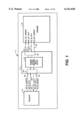
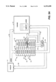
- FIG. 1 is a schematic diagram of a system with a system controller including a random access snooping write buffer of the present invention
- FIG. 2 is a schematic diagram of an embodiment of the random access snooping write buffer of FIG. 1;
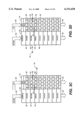
- FIGS. 3A-3E are schematic illustrations depicting stages of the random access snooping write buffer of FIG. 2 for write merging in accordance with the present invention
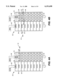
- FIGS. 4A-4E are schematic illustrations depicting stages of the random access snooping write buffer of FIG. 2 for write collapsing in accordance with the present invention.
- FIGS. 5A-5B are schematic illustrations depicting stages of the random access snooping write buffer of FIG. 2 for read merging in accordance with the present invention.
- FIG. 1 shows a system C with a system controller S including a random access snooping write buffer 12 according to the present invention.
- the system controller S may provide a single snooping write buffer 12 or a plurality of snooping write buffers 12.
- the snooping write buffer 12 allows for specialized posting and retrieving of write data.
- a "producer" 10 within the system C provides an input write address 56 and input write data 58 through a producer interface 60 (typically a bus) to the snooping write buffer 12.
- the snooping write buffer 12 In retrieving write data from the snooping write buffer 12, the snooping write buffer 12 provides a write address 52 and write data 54 through a consumer interface 62 (typically a bus) to a "consumer" 14 within the system C.
- the "producer” 10 is a master device for providing data to the slave device or “consumer” 14.
- the "producer” 10 may be a processor or bus master, and the "consumer” 14 may be a memory device, a peripheral device, a memory bus, or a peripheral bus.
- a "producer” and “consumer” include (i) a dynamic random access memory (DRAM) controller and a DRAM, (ii) a processor and a DRAM, (iii) a processor and a Peripheral Component Interconnect (PCI) bus, and (iv) a PCI master and a DRAM. It should be understood that these examples are not exhaustive. Further, certain components of the system C which are not necessary to gain a full understanding of the present invention have been omitted for clarity.
- DRAM dynamic random access memory
- PCI Peripheral Component Interconnect
- the system controller S is a controller for a processor-based system or sub-system which uses write buffering to minimize access time for writing data to a "consumer" 14.
- the system controller S may be an embedded microcontroller. It should be understood that multiple "producers" within the system C may be capable of posting write data to a plurality of snooping write buffers 12 for the "consumer" 14, and that multiple “consumers” within the system C may be capable of retrieving write data from a plurality of snooping write buffers 12. It should also be understood that certain components of the system controller S which are not necessary to gain a full understanding of the present invention have been omitted.
- the write buffer 12 provides a unique write buffer FIFO (First-In-First-Out) architecture for supporting write merging, write collapsing, and read merging.
- the write buffer FIFO architecture of the present invention is an enhancement of a write buffer circular queue FIFO architecture. Accordingly, the disclosed write buffer FIFO is implemented as a circular queue. It is contemplated that a write buffer FIFO architecture according to the present invention may be used to enhance other types of write buffer FIFO architectures.
- A[31:2]) are the same, even if some of the byte enables are different.
- a new rank is allocated and new write data is posted to the new rank.
- the new write data may be provided for an address "related" to an address for which write data is already stored in an existing rank. This event occurs when data was previously posted for an address "related" to an address provided with the new write data. It should be understood that this event may occur for a write buffer of any width and is not specific to a DWORD width write buffer. Multiple write cycles thus have been used to post write data associated with "related" addresses to multiple ranks. Since a FIFO provides a limited number of ranks, each rank constitutes valuable FIFO space.
- the snooping write buffer embodiment 12 includes a write buffer controller 16, a write pointer 18, a read pointer 20, a write address switch 22, a read address switch 24, and a random access memory 30 including a content addressable memory address store 32 and a random access memory data store 34.
- the write buffer controller 16 controls the operation of the snooping write buffer 12.
- the write buffer controller 16 may be implemented as a single integrated controller or a plurality of controllers with each controller regulating a particular structure within the snooping write buffer 12.
- the write buffer controller 16 may include a write buffer load controller, a write buffer fetch controller, a write buffer read pointer controller, and a write buffer write pointer controller.
- the write buffer controller 16 uses a WR -- ADVANCE signal to advance the write pointer 18 and uses a RD -- ADVANCE signal to advance the read pointer 20.
- a content addressable memory also known as associative memory, is a specialized memory allowing for a fast comparison between an address supplied by a requesting master and addresses existing in the content addressable memory.
- the address store 32 may include typical components of a content addressable memory such as a mask register, input register, output register, a storage cell array, match circuitry, and select circuitry.
- Match circuitry is typically implemented but not restricted to using exclusive-nor gates, with each bit of input data for comparison being paired with a bit of the memory element. Design and operation of a content addressable memory is understood in the art.
- an encoder (not shown) of the address store 32 is used to generate the CAM -- HIT -- ADDR signal for identifying a rank address of the address store containing an address "related" to an input address.
- the random access memory 30 may include a full address rank (not shown) including the address tag or write address, byte enable bits for determining the validity of the bytes in the data store 34, an address tag valid bit to reflect the validity of the address tag, and bits used for debugging the snooping write buffer 12.
- a full address rank including the address tag or write address, byte enable bits for determining the validity of the bytes in the data store 34, an address tag valid bit to reflect the validity of the address tag, and bits used for debugging the snooping write buffer 12.
- the address tag which constitutes the address rank for the address array 68 is preferably implemented as content addressable memory. Further, it should be understood that a dedicated valid bit or byte enable bits may be used for excluding an address entry from the compare operation.
- the data store 34 of the snooping write buffer 12 includes a set of ranks 70 shown in dashed and dotted lines for storing write data
- the address store 32 of the snooping write buffer 12 includes a set of ranks 68 shown in dashed and dotted lines for storing write data addresses.
- the set of ranks within the data store 34 serves as an data array
- the set of ranks within the address store 32 serves as an address array.
- Each rank in the data store 34 for storing write data is associated with a rank in the address store 32 for storing a write address or address tag.
- a write address in a rank of the address store 32 is the address for the location in the consumer 14 where the write data in the associated rank of the data store 34 is to be provided.
- Each rank in the address store 32 thus corresponds 1 for 1 to a rank in the data store 34.
- the read pointer 20 points to the "next" rank in the data store 34 where previously written data is to be read
- the write pointer 18 points to the "next" rank in the data store 34 where write data is to be written.
- the write pointer 18 and read pointer 20 are implemented as counters.
- the data store 34 is a dual ported static RAM with the ability to handle concurrent read and write accesses to the data store 34
- the address store 32 is a dual ported static CAM with the ability to handle concurrent read and write accesses to the address store 32.
- the address store 32 and data store 34 of the random access memory 30 may include an address and data posting latch (not shown) for storing an address, byte enables and data retrieved from the write buffer 12. For the consumer 14, this latch is used to prevent stalling the producer 10 should a rank attempt to be written as it is being read out for the consumer 14.
- the write address switch 22 provides an address signal 26 to the address store 32 and data store 34 to select the "next" rank where input write data and address is to be stored
- the read address switch 24 provides an address signal 28 to the address store 32 and data store 34 to select the "next" rank where previously written write data is to be read.
- the input signals to the write address switch 22 include a WR -- ADDR signal from the write pointer 18 providing a rank address within the address store 32 and data store 34 for the next contiguous rank and a CAM -- HIT -- ADDRESS signal for providing a rank address within the address store 32 and data store 34 for a rank storing a write address "related" to the input write address if such a rank exists.
- a first address is "related" to a second address if the addresses are the same as or contiguous with one another such that data for both addresses is capable of storage in a single rank of the data store 34. If the addresses are not contiguous such that data for both addresses is not capable of storage in a single rank of the data store 34, then the addresses are deemed "unrelated.”
- the write address switch 22 is controlled by a WR -- MERGE signal from the write buffer controller 16.
- the state of the WR -- MERGE signal is based on the state of a CAM -- HIT signal provided by the address store 32 to the write buffer controller 16. If an address "related" to the input write address 56 is present in the address store 32, then the CAM -- HIT signal is asserted indicating an address match or hit. If the CAM -- HIT signal is asserted, then the write buffer controller 16 asserts the WR -- MERGE signal provided to the write address switch 22. If the WR -- MERGE signal is asserted at the write address switch 22, the write address switch 22 provides a CAM -- HIT -- ADDR signal to the address store 32 and data store 34.
- the WR -- MERGE signal is active for a write merge in accordance with the present invention and a write collapse in accordance with the present invention.
- the CAM -- HIT -- ADDR signal provides the rank address for a rank containing a write address in the address store 32 and associated data in the data store 34 "related" to the input write address 56 if such a rank address exists. If the CAM -- HIT signal is asserted, then the write buffer controller 16 asserts the WR -- MERGE signal, thus switching the address switch 22 to provide the CAM -- HIT -- ADDR signal.
- an input write address 56 from a producer "related" to existing write addresses in the snooping write buffer 12 may be stored in an existing rank in the address store 32 and the associated data input WR -- IN -- DATA 58 is stored to an existing rank in the data store 34.
- the CAM -- HIT signal is deasserted indicating an address mismatch or miss. If the CAM -- HIT signal is deasserted, then the write buffer controller 16 deasserts the WR -- MERGE signal provided to the write address switch 22. If the WR -- MERGE signal is deasserted at the write address switch 22, the write address switch 22 provides the WR -- ADDR signal to the address store 32 and data store 34. Also, if the CAM -- HIT signal is deasserted, then the write buffer controller 16 advances the write pointer 18 to the next contiguous rank address.
- the input signals to the read address switch 24 include a READ -- ADDR signal providing a rank address within the address store 32 for the next contiguous rank from the read pointer 20 and a CAM -- HIT -- ADDRESS signal for providing an address within the address store 32 for a rank containing a write address "related" to the input read address 64 (FIGS. 5A-5B) if such a rank address exists. It should be understood that the WR -- IN -- ADDRESS signal and RD -- IN -- ADDRESS signal may constitute the same bus.
- the read address switch 24 is controlled by a RD -- MERGE signal from the write buffer controller 16. The state of the RD -- MERGE signal is based on the state of the CAM -- HIT signal provided by the address store 32 to the write buffer controller 16.
- the CAM -- HIT signal is asserted indicating an address match or hit. If the CAM -- HIT signal is asserted, then the write buffer controller 16 asserts the RD -- MERGE signal provided to the read address switch 24. If the RD -- MERGE signal is asserted at the read address switch 24, the read address switch 22 provides a CAM -- HIT -- ADDR signal to the data store 34 and address store 32.
- the CAM -- HIT -- ADDR signal provides a rank address within the address store 32 for a rank containing a write address "related" to the input read address 64 if such a rank address exists.
- the CAM -- HIT -- ADDR signal may be used to retrieve byte enables which indicate the rank address of the data to be merged. If the CAM -- HIT signal is asserted, then the write buffer controller 16 asserts the RD -- MERGE signal, thus switching the address switch 24 to provide the CAM -- HIT -- ADDR signal.
- a write data address in the address store 32 "related" to an input read address may be retrieved from the data store 34. The retrieved data may then be merged with data from the consumer 14 associated with the input read address 64 to provide coherent data to the producer 10.
- the CAM -- HIT signal is deasserted indicating an address mismatch or miss. If the CAM -- HIT signal is deasserted, then the write buffer controller 16 deasserts the RD -- MERGE signal provided to the read address switch 24. If the RD -- MERGE signal is deasserted at the read address switch 24, the read address switch 24 provides the RD -- ADDR signal to the address store 32 and data store 34. In the disclosed embodiment, the read address switch 24 and write address switch 22 are implemented as multiplexers.
- the write buffer controller 16 advances the read pointer 20 after data is placed in the posting latch (not shown) which is going to the consumer 14. If the producer read cycle results in a write buffer "miss" then the consumer 14 supplies the data and the write buffer read merge does not take place, since the consumer 14 has the most recent data.
- the write buffer controller 16 controls posting of input addresses associated with write data through a WR -- STROBE signal.
- the address bus WR -- IN -- ADDRESS 15 is connected to the input lines of the memory cells for storage into the CAM.
- the WR -- IN -- ADDRESS signal is written into the CAM memory cells on an active WR -- STROBE signal.
- the address bus 15 is also connected to a CAM query side of the CAM so that an address driven onto the bus 15 may be compared with the contents already stored in the memory cells. For a read, the CAM does not latch an address, the RD -- IN -- ADDRESS signal, into a memory cell. In this case, the WR -- STROBE signal is not active because the cycle is a read cycle. An address, however, is still used for the CAM query to detect if there is an address already in the CAM that matches an address presented by the producer 10.
- An input address enters the address store 32 through an address port 74.
- the write buffer 12 may receive an ADDRESS signal for a read or write operation.
- the ADDRESS signal is provided to both the write buffer 12 and the consumer 14.
- a write address exits the address store 32 through an address port 76 as a WR -- OUT -- ADDRESS signal.
- a read address exits the address store 32 through the address port 76 as a RD -- OUT -- ADDRESS signal.
- the write buffer 12 may prove a WRITE -- BUFFER -- ADDRESS signal to the consumer 14, the consumer 14 including a multiplexer for selecting either a producer address or the WRITE -- BUFFER -- ADDRESS signal carrying a write buffer address.
- Each rank of the address array 68 is coupled to a common address bus (not shown). Inputs to memory cells of the CAM share the same memory bus and, outputs from the memory cells of the CAM share the same bus allowing for random access capability for write buffer data and addresses. Random access capability allows a write address to be stored or retrieved from any rank in the address array 68.
- Write data from a producer 10 enters the data array 70 through a data port 78 as a WR -- IN -- DATA signal WR -- IN -- DATA is latched into the data store 37 when the WR -- STROBE signal is active. Write data exits the data array 70 through a data port 80 as a WR -- OUT -- DATA signal.
- Each rank of the data array 70 is coupled to a common data bus (not shown). Random access capability allows write data to be posted or retrieved from any rank in the data array 70 or address array 68.
- the data store 34 may include typical components of a random access memory.
- the snooping write buffer 12 may include configuration registers (not shown) for configuring the system modes in which the write buffer 12 is enabled and to define address regions in the system C as bufferable or non-bufferable.
- FIGS. 3A-3E exemplary illustrations depicting stages of the write snooping buffer 12 showing write merging in accordance with the present invention are shown.
- an address rank 36 of the address array 68 is storing a write address ⁇ 2c5fa88 ⁇ and a data rank 38 of the data array 70 is storing write data ⁇ 3b4ec82a ⁇ .
- FIG. 3A also shows the producer 10 presenting a new write address 56 of ⁇ 4a37be0 ⁇ to the address array 68 with new input write data 58 of ⁇ a369 - - - ⁇ to the data array 70.
- a ⁇ - ⁇ represents don't care data.
- the reason this data is "don't care" data is that corresponding ones of the byte enables BE3-0# are deasserted.
- the write pointer 18 is pointing to the address rank 36 and the data rank 38.
- FIG. 3B a stage of the random access memory 30 a single write cycle after the stage of FIG. 3A is shown.
- the write address ⁇ 4a37be0 ⁇ was written into the address rank 40, the next contiguous rank after the address rank that was pointed to by the write pointer 18 in FIG. 3A.
- the write data ⁇ a369 - - - ⁇ was written into the data rank 42, the next contiguous rank after the data rank that was pointed to by the write pointer 18 in FIG. 3A.
- write data ⁇ a369 ⁇ represents valid data
- write data ⁇ XXXX ⁇ represents invalid data.
- FIG. 3B also shows the producer 10 presenting a new write address 56 of ⁇ 5b6fe7c ⁇ to the address array 68 with new input write data 58 of ⁇ 6e7b8d9a ⁇ to the data array 70.
- the address ⁇ 4a37be0 ⁇ was concurrently compared to the write addresses stored in the address array 68 to detect if an address "related" to the write address ⁇ 4a37be0 ⁇ was present in the address array 68.
- a concurrent compare operation in accordance with the present invention may include comparing each bit or selective bits of an input write address with each bit or selective bits of write address stored in the address array 68.
- address bits A31 through A2 of a 32-bit address bus are compared for an input address and a stored write address.
- the two lowest order bits on the address bus, A1 and A0 serve as byte enable bits. Since the stored write address ⁇ 2c5fa88 ⁇ was "unrelated" to the write address ⁇ 4a37be0 ⁇ , the CAM -- HIT signal was deasserted indicating an address miss. In response to the deasserted CAM -- HIT signal, the write buffer controller 16 deasserted the WR -- MERGE signal. In response to the deasserted WR -- MERGE signal, the write address switch 22 provided the WR -- ADDR signal to the address store 32. The WR -- ADDR signal represents the next contiguous rank address which in this case was address rank 40 and data rank 42.
- FIG. 3C a stage of the random access memory 30 a single write cycle after the stage of FIG. 3B is shown.
- the write address ⁇ 5b6fe7c ⁇ was written into address rank 44, the next contiguous rank after the address rank pointed to by the write pointer 18 in FIG. 3B.
- FIG. 3C also shows the producer 10 presenting a new write address 56 of a ⁇ 4a37be0 ⁇ to the address array 68 with new input write data 58 of ⁇ - - - 52cc ⁇ to the data array 70.
- the write address ⁇ 5b6fe7c ⁇ was concurrently compared to the write addresses stored in the address array 68 to detect if an address "related" to the write address ⁇ 5b6fe7c ⁇ was present in the address array 68. Since the write address ⁇ 5b6fe7c0 ⁇ was "unrelated" to the write addresses ⁇ 2c5fa88 ⁇ and ⁇ 4a37be0 ⁇ , the CAM -- HIT signal was deasserted indicating an address miss.
- the write buffer controller 16 deasserts the WR -- MERGE signal.
- the write address switch 2 provided the WR -- ADDR signal.
- the WR -- ADDR signal represents the next contiguous rank address which in this case was for address rank 44 and data rank 46.
- the write address ⁇ 4a37be0 ⁇ is concurrently compared to the write addresses stored in the address array 68 to detect if an address "related" to the write address ⁇ 4a37be0 ⁇ is present in the address array 68.
- the write address ⁇ 4a37be0 ⁇ is related to the write address ⁇ 4a37be0 ⁇ stored in the address rank 40 since the addresses are contiguous such that data for both addresses may be stored in a single rank.
- bits A31-A2 of both addresses are compared.
- the CAM -- HIT signal is asserted indicating an address hit or match.
- the write buffer controller 16 asserted the WR -- MERGE signal.
- the write address switch 22 provides the CAM -- HIT -- ADDR signal to the address store 32 and data store 34.
- the CAM -- HIT -- ADDR signal represents the rank address corresponding to the detected "related" address.
- the rank address in this case is for address rank 40 and data rank 42.
- the write pointer 26 (output of switch 22) provides an address to any allocated address rank and data rank in the random access snooping write buffer 12 corresponding to a write address "related" to the input write address 56.
- the allocated address and data ranks in the snooping write buffer 12 are those ranks pointed to by the read pointer 20 and the ranks between the read pointer 20 and the write pointer 18.
- the rank pointed to by the write pointer 18 is not allocated since the write pointer 18 points to the "next" space to potentially write into.
- FIG. 3E a stage of the random access memory 30 following the stage of FIG. 3D is shown.
- the write addresses ⁇ 4a37be0 ⁇ is stored in address rank 40 and the write data ⁇ - - - 52cc ⁇ is merged with the write data ⁇ a369 - - - ⁇ already stored in the data rank 42 producing the write data ⁇ a36952cc ⁇ . Since invalid data was replaced with valid data ⁇ 52cc, ⁇ the valid bits corresponding to write data ⁇ 52cc ⁇ are switched to a valid state from an invalid state.
- By write merging data for "related" addresses using the random access snooping write buffer 12 a savings in FIFO space is achieved.
- the write data is posted to a single rank.
- the savings in FIFO space through write merging is a function of the size of the write data posted for "related" addresses. For example, if a rank is the size of a doubleword, four write cycles may be used to post write data to a single rank if the write data posted for each write cycle is the size of a byte and is non-overlapping. In accordance with the present invention, this example results in a 4:1 savings in FIFO space. It should be understood that a write data location of smaller size than a rank may be individually addressable. Write merging using the random access snooping write buffer 12 also reduces the number of read cycles for retrieving write data for "related" addresses.
- storing write data for "related" addresses across multiple ranks in a conventional write buffer FIFO scatters write traffic.
- Storing write data for "related" addresses to a single rank in accordance with the present invention consolidates write traffic.
- splitting "related" addresses across multiple ranks in a conventional write buffer FIFO under-utilizes a write buffer rank. For example, if a write buffer rank has a four byte size, consecutive single byte transfers result in four write buffer ranks with only one byte of each rank storing a byte a data. In this case, at most only 25% of a write buffer rank contains data.
- a write buffer rank is fully utilized if write data having "related" addresses is posted to the write buffer.
- FIGS. 4A-4E exemplary illustrations depicting stages of the random access write snooping buffer 12 showing write collapsing in accordance with the present invention are shown.
- an address rank 36 of the address array 68 is storing a write address ⁇ 2c5fa88 ⁇ and a data rank 38 of the data array 70 is storing write data ⁇ 3b4ec82a ⁇ .
- FIG. 4a also shows the producer 10 presenting a new write address 56 of ⁇ 4a37be0 ⁇ to the address array 68 with new input write data 58 of ⁇ a36941ff ⁇ to the data array 70.
- the write pointer 18 is pointing to the address rank 36 and the data rank 38.
- FIG. 4B a stage of the random access memory 30 a single write cycle after the stage of FIG. 4A is shown.
- the write address ⁇ 4a37be0 ⁇ was written into the address rank 40, the next contiguous rank after the address rank that was pointed to by the write pointer 18 in FIG. 4A.
- the write data ⁇ a36941ff ⁇ was written into the data rank 42, the next contiguous rank to the data rank that was pointed to by the write pointer 18 in FIG. 4A.
- the valid bits corresponding to write data ⁇ a36941ff ⁇ are in a valid state.
- 4B also shows the producer 10 presenting a new write address 56 of ⁇ 5b6fe7c ⁇ to the address array 68 with a new input write data 58 of ⁇ 6e7b8d9a ⁇ to the data array 70.
- the address ⁇ 4a37be0 ⁇ was concurrently compared to the write addresses stored in the address array 68 to detect if an address "related" to the write address ⁇ 4a37be0 ⁇ was present in the address array 68.
- the CAM -- HIT signal was deasserted indicating an address miss.
- the write buffer controller 16 deasserted the WR -- MERGE signal.
- the write address switch 22 provided the WR -- ADDR signal to the address store 32 and data store 34.
- the WR -- ADDR signal represents the next contiguous rank address which in this case was address rank 40 and data rank 42.
- FIG. 4C a stage of the random access memory 30 a write cycle after the stage of FIG. 4B is shown.
- the write address ⁇ 5b6fe7c ⁇ was written into address rank 44, the next contiguous rank after the address rank pointed to by the write pointer in FIG. 4B.
- the write data ⁇ 6e7b8d9a ⁇ was written into data rank 46, the next contiguous rank after the data rank pointed to by the write pointer in FIG. 4B.
- FIG. 4C also shows the producer 10 presenting a new write address 56 of ⁇ 4a37be0 ⁇ to the address array 68 with new input write data 58 of ⁇ - - - 52cc ⁇ to the data array 70.
- the write address ⁇ 5b6fe7c ⁇ was concurrently compared to the write addresses stored in the address array 68 to detect if an address "related" to the write address ⁇ 5b6fe7c ⁇ was present in the address array 68. Since the write address ⁇ 5b6fe7c ⁇ was "unrelated" to the write addresses ⁇ 2c5fa89 ⁇ and ⁇ 4a37be0 ⁇ , the CAM -- HIT signal was deasserted indicating an address miss. In response to the deasserted CAM -- HIT signal, the write buffer controller 16 deasserted the WR -- MERGE signal. In response to the deasserted WR -- MERGE signal, the write address switch 22 provided the WR -- ADDR signal. The WR -- ADDR signal represents the next contiguous rank address which in this case was for address rank 44 and data rank 46.
- the write address ⁇ 4a37be0 ⁇ is concurrently compared to the write addresses stored in the address array 68 to detect if an address "related" to the write address ⁇ 4a37be0 ⁇ was present in the address array 68.
- the write address ⁇ 4a37be0 ⁇ is related to the write address ⁇ 4a37be0 ⁇ stored in the address rank 40 since the addresses are contiguous such that data for both addresses may be stored in a single rank. Since a "related" address is present in the address array 68, the CAM -- HIT signal is asserted indicating an address hit or match.
- the write buffer controller 16 In response to the asserted CAM -- HIT signal, the write buffer controller 16 asserts the WR -- MERGE signal. In response to the WR -- MERGE signal, the write address switch 22 provides the CAM -- HIT -- ADDR signal to the address store 32 and data store 34.
- the CAM -- HIT -- ADDR signal represents the rank address corresponding to the detected "related" address. The rank address in this case is for address rank 40 and data rank 42.
- the pointer 26 (output of switch 22) provides an address to any valid address rank and data rank in the snooping write buffer 12 corresponding to a write address "related" to the input write address 56 independent of the present rank pointed to by the write pointer 18. It should be understood that an "X" within the address array 68 or data array 70 represents non-existing data.
- FIG. 4E a stage of the random access memory 30 following the stage of FIG. 4D is shown.
- the write address ⁇ 4a37be0 ⁇ is stored in address rank 40 and the write data ⁇ - - - 52cc ⁇ is combined with the write data ⁇ a36941ff ⁇ already stored in the data rank 42 producing the write data ⁇ a36952cc ⁇ . Since the write data values are overlapping such that both write data values include some valid data, combining the write data values constitutes write collapsing. For this particular example, combining the addresses results in an overwrite of write data ⁇ a36941ff ⁇ with write data ⁇ a36952cc ⁇ .
- a savings in FIFO space is achieved.
- the savings in FIFO space through write collapsing is a function of the number of multiple cycles used to post write data for "related" addresses as write collapsing uses a single rank rather than multiple ranks (new rank used for each write cycle) to post write data for "related" addresses.
- Savings in FIFO space through write collapsing may be greater than savings in FIFO space through write merging.
- Write collapsing in contrast to merging, allows for incoming valid data to be written to a byte location or locations already storing valid data.
- write collapsing may result in a partial write collapse whereby one portion of valid data is written to a location storing valid data and another portion of valid data is written to a location storing invalid data. Further write collapsing, like write merging, may reduce the number of read cycles for retrieving write data for "related" addresses.
- FIGS. 5A-5B exemplary illustrations depicting stages of the random access snooping write buffer 12 showing read merging in accordance with the present invention is shown.
- an input read address 64 is provided to the address array 68 and the consumer 14 by the producer 10.
- the input read address 64 is provided to the consumer 14 to read data in the consumer 14 corresponding to the input read address 64.
- the input write address is ⁇ a000000 ⁇ .
- the data stored at this address in the consumer 14 is ⁇ ee001122 ⁇ .
- the input read address 64 is also provided to the address array 68 for concurrent comparison to the write addresses stored in the address array 68.
- any address in the address array 68 "related" to the input read address 64 may be detected.
- the write address ⁇ a000000 ⁇ stored in rank 72 is "related" to the input read address ⁇ a000000 ⁇ . Since a related address is present in the address array 68, the CAM -- HIT signal is asserted indicating an address hit (FIG. 2).
- the write buffer controller 16 asserts the RD -- MERGE signal.
- the read address switch 24 provides the CAM -- HIT -- ADDR signal to the address store 32 and data store 34.
- the CAM -- HIT -- ADDR signal represents the rank address corresponding to the detected "related" address which in this case is for address rank 72 and data rank 73.
- the pointer 28 (output of switch 24) provides an address to the address store 32 and data store 34 of any valid address rank and data rank in the snooping work buffer 12 corresponding to a read address "related" to the input read address independent of the present rank pointed to by the read pointer 20.
- Data rank 73 stores the write data ⁇ xxxxcdef. ⁇
- the two least significant bytes, ⁇ cdef ⁇ , of the write data corresponds to valid data as indicated by valid bits 96 having a valid state.
- the two most significant bytes, ⁇ xxxx, ⁇ of the write data corresponds to invalid data as indicated by valid bits 98 having an invalid state.
- the write data ⁇ xxxxcdef ⁇ is provided from the data array 70 to a read merge generator 60 as a RD -- OUT -- ADDRESS signal 62.
- the read merge generator 60 also receives read data 63 for the address ⁇ a000000 ⁇ from the consumer 14.
- the read merge generator 60 performs a read merge operation by combining read data 63 from the consumer 14 with a valid portion read data 62 from the data store 70 when the address store 68 includes an address "related" to the input read address 64.
- the valid portion of read data 62 from the data store, ⁇ cdef, ⁇ replaces the corresponding portion of read data 63 from the consumer 14, ⁇ 1122 ⁇ .
- the read merge generator 60 thus filters out any invalid portion of read data 62 and any portion of read data 63 corresponding to a valid portion of read data 62.
- the read merge generator 60 is implemented as a multiplexer.
- write data, write addresses, and read data described in the above examples are illustrative. Further, while each illustrated data rank is shown with a four byte, or double word, size, it should be understood that the number and size of ranks provided for the data array 68 and the address array 70 and the size of write data and write addresses may vary for the snooping write buffer 12 of the present invention. In addition, it is contemplated that write merging, write collapsing, and read merging as described above may be provided as a basic or enhanced mode of a write buffer.
- the write buffer of present invention may have a disable mode preventing write buffering, an enable mode allowing general write buffering, and an enhanced enable mode for write buffering supporting write merging, write collapsing, and read merging as described above. Further, it should be understood that in certain situations such as when there is an address hit to a non-bufferable region of a consumer, write merging and read merging may not be desirable. Lastly, it should be understood that the snooping write buffer 12 may be implemented as a synchronous or asynchronous write buffer.
- the present invention thus provides a write buffer 12 with random access memory snooping capability supporting write merging, write collapsing, and read merging.
- the disclosed write buffer embodiment 12 includes a write buffer controller 16 and a random access memory 30 containing a content addressable memory address store 32 and a random access memory data store 34.
- a producer 10 provides the address store 32 with an input write address 56 and input write data 58.
- the CAM 32 concurrently compares the input write address 56 to the addresses present in the address store 32. If the input write address 56 is "related" to an address present in the address store 32, the CAM 32 detects an address hit.
- the indication of an address hit is provided to the write buffer controller 16 which signals the data store 34 to store the input write data in the rank of the data store 34 associated with the "related" address detected by the controller 16. If the input write data 58 does not overlap the data previously stored in the rank associated with the "related" address, the store operation results in write merging. If the input write data 58 overlaps the data previously stored in the rank associated with the rank associated with the "related" address, the store operation results in write collapsing.
- the write buffer 12 thus eliminates the need to allocate a new rank to store write data when an input write address 56 is "related" to an address present in the address store 32.
- the write buffer 12 By storing write data for "related" addresses in a single rank rather than multiple ranks, the write buffer 12 provides for efficient storage of write data for "related" addresses. By eliminating the use of multiple ranks for storing write data for "related" addresses, the write buffer 12 also reduces the number of read cycles for retrieving write data for "related" addresses.
- the CAM 32 detects whether an input read address 64 provided by a producer 10 to a consumer 14 is "related" to any address in the address store 32. If the input read address 64 is "related" to an address present in the address store 32, the write data in the data store 34 associated with the "related" address is merged with valid and invalid read data from the consumer 14 associated with the input read address, thereby resulting in read merging.
- the merged data preserves read data coherency by reflecting the most recent write data in the write buffer 12 and the valid read data in the consumer 14.
- Read merging for data having "related" addresses using a write buffer in accordance with the present invention also eliminates the need to flush a write buffer to maintain coherency, resulting in an increased performance response for such a read cycle.
- a buffer 12 with random access snooping capability thus significantly improves the method of posting and retrieving data for a write buffer by supporting write merging, write collapsing, and read merging.
Abstract
Description
Claims (20)
Priority Applications (2)
| Application Number | Priority Date | Filing Date | Title |
|---|---|---|---|
| US09/008,394 US6151658A (en) | 1998-01-16 | 1998-01-16 | Write-buffer FIFO architecture with random access snooping capability |
| PCT/US1998/015085 WO1999036849A1 (en) | 1998-01-16 | 1998-07-22 | Write-buffer fifo architecture with random access snooping capability |
Applications Claiming Priority (1)
| Application Number | Priority Date | Filing Date | Title |
|---|---|---|---|
| US09/008,394 US6151658A (en) | 1998-01-16 | 1998-01-16 | Write-buffer FIFO architecture with random access snooping capability |
Publications (1)
| Publication Number | Publication Date |
|---|---|
| US6151658A true US6151658A (en) | 2000-11-21 |
Family
ID=21731396
Family Applications (1)
| Application Number | Title | Priority Date | Filing Date |
|---|---|---|---|
| US09/008,394 Expired - Lifetime US6151658A (en) | 1998-01-16 | 1998-01-16 | Write-buffer FIFO architecture with random access snooping capability |
Country Status (2)
| Country | Link |
|---|---|
| US (1) | US6151658A (en) |
| WO (1) | WO1999036849A1 (en) |
Cited By (24)
| Publication number | Priority date | Publication date | Assignee | Title |
|---|---|---|---|---|
| US6304924B1 (en) * | 1999-02-02 | 2001-10-16 | International Business Machines Corporation | Two lock-free, constant-space, multiple-(impure)-reader, single-writer structures |
| US20020118882A1 (en) * | 1998-10-15 | 2002-08-29 | Yasuo Tezuka | Buffer control method and buffer control device |
| US20030067472A1 (en) * | 2001-10-09 | 2003-04-10 | William Radke | Embedded memory system and method including data error correction |
| US6556952B1 (en) * | 2000-05-04 | 2003-04-29 | Advanced Micro Devices, Inc. | Performance monitoring and optimizing of controller parameters |
| US6678838B1 (en) * | 1999-08-23 | 2004-01-13 | Advanced Micro Devices, Inc. | Method to track master contribution information in a write buffer |
| KR100422141B1 (en) * | 2000-12-28 | 2004-03-10 | 엘지전자 주식회사 | Method for constructing ring queue by using SRAM |
| US20040093605A1 (en) * | 1998-11-13 | 2004-05-13 | Alverson Gail A. | Accessing a collection of data items in a multithreaded environment |
| WO2004059499A2 (en) * | 2002-12-30 | 2004-07-15 | Koninklijke Philips Electronics N.V. | Memory controller and method for writing to a memory |
| US6784889B1 (en) | 2000-12-13 | 2004-08-31 | Micron Technology, Inc. | Memory system and method for improved utilization of read and write bandwidth of a graphics processing system |
| US20040210663A1 (en) * | 2003-04-15 | 2004-10-21 | Paul Phillips | Object-aware transport-layer network processing engine |
| EP1555620A1 (en) * | 2003-04-15 | 2005-07-20 | Sun Microsystems, Inc. | Stream Memory manager |
| US20060090043A1 (en) * | 2004-10-21 | 2006-04-27 | International Business Machines Corporation | Handling of TxEna in an XDRTM memory controller |
| US20060123187A1 (en) * | 2004-12-02 | 2006-06-08 | International Business Machines Corporation | Memory controller to utilize DRAM write buffers |
| US20060143406A1 (en) * | 2004-12-27 | 2006-06-29 | Chrysos George Z | Predictive early write-back of owned cache blocks in a shared memory computer system |
| US20060277391A1 (en) * | 2005-06-01 | 2006-12-07 | Microsoft Corporation | Execution model for parallel computing |
| US20070011436A1 (en) * | 2005-06-01 | 2007-01-11 | Microsoft Corporation | Content addressable memory architecture |
| CN100370409C (en) * | 2004-11-18 | 2008-02-20 | 国际商业机器公司 | Method and apparatus for calibrating random access memory |
| US20080115039A1 (en) * | 2006-10-31 | 2008-05-15 | Intel Corporation | Destination indication to aid in posted write buffer loading |
| US20090300338A1 (en) * | 2008-05-28 | 2009-12-03 | Sun Microsystems, Inc. | Aggressive store merging in a processor that supports checkpointing |
| US7707387B2 (en) | 2005-06-01 | 2010-04-27 | Microsoft Corporation | Conditional execution via content addressable memory and parallel computing execution model |
| US20120317353A1 (en) * | 2011-06-13 | 2012-12-13 | XtremlO Ltd. | Replication techniques with content addressable storage |
| US9910621B1 (en) | 2014-09-29 | 2018-03-06 | EMC IP Holding Company LLC | Backlogging I/O metadata utilizing counters to monitor write acknowledgements and no acknowledgements |
| US10101943B1 (en) * | 2014-09-25 | 2018-10-16 | EMC IP Holding Company LLC | Realigning data in replication system |
| US11301170B2 (en) * | 2020-03-05 | 2022-04-12 | International Business Machines Corporation | Performing sub-logical page write operations in non-volatile random access memory (NVRAM) using pre-populated read-modify-write (RMW) buffers |
Families Citing this family (1)
| Publication number | Priority date | Publication date | Assignee | Title |
|---|---|---|---|---|
| US10169273B2 (en) * | 2017-01-11 | 2019-01-01 | Qualcomm Incorporated | Forced compression of single I2C writes |
Citations (8)
| Publication number | Priority date | Publication date | Assignee | Title |
|---|---|---|---|---|
| US4538226A (en) * | 1983-01-27 | 1985-08-27 | Nec Corporation | Buffer control system |
| US4750154A (en) * | 1984-07-10 | 1988-06-07 | Prime Computer, Inc. | Memory alignment system and method |
| US4959771A (en) * | 1987-04-10 | 1990-09-25 | Prime Computer, Inc. | Write buffer for a digital processing system |
| US5299147A (en) * | 1993-02-22 | 1994-03-29 | Intergraph Corporation | Decoder scheme for fully associative translation-lookaside buffer |
| WO1994011828A2 (en) * | 1992-11-09 | 1994-05-26 | Ast Research, Inc. | Write buffer with full rank byte gathering |
| US5329405A (en) * | 1989-01-23 | 1994-07-12 | Codex Corporation | Associative cam apparatus and method for variable length string matching |
| US5517660A (en) * | 1990-04-12 | 1996-05-14 | Digital Equipment Corporation | Read-write buffer for gathering write requests and resolving read conflicts based on a generated byte mask code |
| US5627993A (en) * | 1994-10-21 | 1997-05-06 | International Business Machines Corporation | Methods and systems for merging data during cache checking and write-back cycles for memory reads and writes |
-
1998
- 1998-01-16 US US09/008,394 patent/US6151658A/en not_active Expired - Lifetime
- 1998-07-22 WO PCT/US1998/015085 patent/WO1999036849A1/en active Application Filing
Patent Citations (8)
| Publication number | Priority date | Publication date | Assignee | Title |
|---|---|---|---|---|
| US4538226A (en) * | 1983-01-27 | 1985-08-27 | Nec Corporation | Buffer control system |
| US4750154A (en) * | 1984-07-10 | 1988-06-07 | Prime Computer, Inc. | Memory alignment system and method |
| US4959771A (en) * | 1987-04-10 | 1990-09-25 | Prime Computer, Inc. | Write buffer for a digital processing system |
| US5329405A (en) * | 1989-01-23 | 1994-07-12 | Codex Corporation | Associative cam apparatus and method for variable length string matching |
| US5517660A (en) * | 1990-04-12 | 1996-05-14 | Digital Equipment Corporation | Read-write buffer for gathering write requests and resolving read conflicts based on a generated byte mask code |
| WO1994011828A2 (en) * | 1992-11-09 | 1994-05-26 | Ast Research, Inc. | Write buffer with full rank byte gathering |
| US5299147A (en) * | 1993-02-22 | 1994-03-29 | Intergraph Corporation | Decoder scheme for fully associative translation-lookaside buffer |
| US5627993A (en) * | 1994-10-21 | 1997-05-06 | International Business Machines Corporation | Methods and systems for merging data during cache checking and write-back cycles for memory reads and writes |
Non-Patent Citations (4)
| Title |
|---|
| AMD 640 System Controller Data Sheet , Advanced Micro Devices, Inc., 1997, pp. 2 1 through 2 4, 5 1 through 5 3, 5 11, and 5 32. * |
| AMD-640 System Controller Data Sheet, Advanced Micro Devices, Inc., © 1997, pp. 2-1 through 2-4, 5-1 through 5-3, 5-11, and 5-32. |
| Motorola Semiconductor Technical Data , Motorola, Inc., Doc. No. MCM69C432, Rev. 2, Sep. 15, 1997, pp. 1 20. * |
| Motorola Semiconductor Technical Data, Motorola, Inc., Doc. No. MCM69C432, Rev. 2, Sep. 15, 1997, pp. 1-20. |
Cited By (57)
| Publication number | Priority date | Publication date | Assignee | Title |
|---|---|---|---|---|
| US6826354B2 (en) * | 1998-10-15 | 2004-11-30 | Fujitsu Limited | Buffer control method and buffer control device |
| US20020118882A1 (en) * | 1998-10-15 | 2002-08-29 | Yasuo Tezuka | Buffer control method and buffer control device |
| US7558910B2 (en) * | 1998-11-13 | 2009-07-07 | Cray Inc. | Detecting access to a memory location in a multithreaded environment |
| US7558889B2 (en) | 1998-11-13 | 2009-07-07 | Cray Inc. | Accessing a collection of data items in a multithreaded environment |
| US7904685B1 (en) | 1998-11-13 | 2011-03-08 | Cray Inc. | Synchronization techniques in a multithreaded environment |
| US20050021898A1 (en) * | 1998-11-13 | 2005-01-27 | Alverson Gail A. | Detecting access to a memory location in a multithreaded environment |
| US20040093605A1 (en) * | 1998-11-13 | 2004-05-13 | Alverson Gail A. | Accessing a collection of data items in a multithreaded environment |
| US6304924B1 (en) * | 1999-02-02 | 2001-10-16 | International Business Machines Corporation | Two lock-free, constant-space, multiple-(impure)-reader, single-writer structures |
| US6678838B1 (en) * | 1999-08-23 | 2004-01-13 | Advanced Micro Devices, Inc. | Method to track master contribution information in a write buffer |
| US6556952B1 (en) * | 2000-05-04 | 2003-04-29 | Advanced Micro Devices, Inc. | Performance monitoring and optimizing of controller parameters |
| US7916148B2 (en) | 2000-12-13 | 2011-03-29 | Round Rock Research, Llc | Memory system and method for improved utilization of read and write bandwidth of a graphics processing system |
| US20100220103A1 (en) * | 2000-12-13 | 2010-09-02 | Round Rock Research, Llc | Memory system and method for improved utilization of read and write bandwidth of a graphics processing system |
| US20110169846A1 (en) * | 2000-12-13 | 2011-07-14 | Round Rock Research, Llc | Memory system and method for improved utilization of read and write bandwidth of a graphics processing system |
| US20080218525A1 (en) * | 2000-12-13 | 2008-09-11 | William Radke | Memory system and method for improved utilization of read and write bandwidth of a graphics processing system |
| US6784889B1 (en) | 2000-12-13 | 2004-08-31 | Micron Technology, Inc. | Memory system and method for improved utilization of read and write bandwidth of a graphics processing system |
| US20050024367A1 (en) * | 2000-12-13 | 2005-02-03 | William Radke | Memory system and method for improved utilization of read and write bandwidth of a graphics processing system |
| US8446420B2 (en) | 2000-12-13 | 2013-05-21 | Round Rock Research, Llc | Memory system and method for improved utilization of read and write bandwidth of a graphics processing system |
| US8194086B2 (en) | 2000-12-13 | 2012-06-05 | Round Rock Research, Llc | Memory system and method for improved utilization of read and write bandwidth of a graphics processing system |
| US7379068B2 (en) | 2000-12-13 | 2008-05-27 | Micron Technology, Inc. | Memory system and method for improved utilization of read and write bandwidth of a graphics processing system |
| US7724262B2 (en) | 2000-12-13 | 2010-05-25 | Round Rock Research, Llc | Memory system and method for improved utilization of read and write bandwidth of a graphics processing system |
| KR100422141B1 (en) * | 2000-12-28 | 2004-03-10 | 엘지전자 주식회사 | Method for constructing ring queue by using SRAM |
| US20040183808A1 (en) * | 2001-10-09 | 2004-09-23 | William Radke | Embedded memory system and method including data error correction |
| US6956577B2 (en) | 2001-10-09 | 2005-10-18 | Micron Technology, Inc. | Embedded memory system and method including data error correction |
| US20030067472A1 (en) * | 2001-10-09 | 2003-04-10 | William Radke | Embedded memory system and method including data error correction |
| US6741253B2 (en) * | 2001-10-09 | 2004-05-25 | Micron Technology, Inc. | Embedded memory system and method including data error correction |
| CN1732446B (en) * | 2002-12-30 | 2010-09-08 | Nxp股份有限公司 | Method for writing to a memory |
| US7568082B2 (en) * | 2002-12-30 | 2009-07-28 | Jan Hoogerbrugge | Memory controller and method for writing to a memory |
| US20060106969A1 (en) * | 2002-12-30 | 2006-05-18 | Koninklijke Philips Electronics N.V. | Memory controller and method for writing to a memory |
| WO2004059499A3 (en) * | 2002-12-30 | 2004-09-02 | Koninkl Philips Electronics Nv | Memory controller and method for writing to a memory |
| WO2004059499A2 (en) * | 2002-12-30 | 2004-07-15 | Koninklijke Philips Electronics N.V. | Memory controller and method for writing to a memory |
| US20040210663A1 (en) * | 2003-04-15 | 2004-10-21 | Paul Phillips | Object-aware transport-layer network processing engine |
| US20050060414A1 (en) * | 2003-04-15 | 2005-03-17 | Sun Microsystems, Inc. | Object-aware transport-layer network processing engine |
| US20050060427A1 (en) * | 2003-04-15 | 2005-03-17 | Sun Microsystems, Inc. | Object-aware transport-layer network processing engine |
| EP1555620A1 (en) * | 2003-04-15 | 2005-07-20 | Sun Microsystems, Inc. | Stream Memory manager |
| US20080046620A1 (en) * | 2004-10-21 | 2008-02-21 | Bellows Mark D | Handling of the Transmit Enable Signal in a Dynamic Random Access Memory Controller |
| US7275137B2 (en) * | 2004-10-21 | 2007-09-25 | International Business Machines Corporation | Handling of the transmit enable signal in a dynamic random access memory controller |
| US20060090043A1 (en) * | 2004-10-21 | 2006-04-27 | International Business Machines Corporation | Handling of TxEna in an XDRTM memory controller |
| US7631154B2 (en) | 2004-10-21 | 2009-12-08 | International Business Machines Corporation | Handling of the transmit enable signal in a dynamic random access memory controller |
| CN100370409C (en) * | 2004-11-18 | 2008-02-20 | 国际商业机器公司 | Method and apparatus for calibrating random access memory |
| US8219745B2 (en) * | 2004-12-02 | 2012-07-10 | International Business Machines Corporation | Memory controller to utilize DRAM write buffers |
| US20060123187A1 (en) * | 2004-12-02 | 2006-06-08 | International Business Machines Corporation | Memory controller to utilize DRAM write buffers |
| US20060143406A1 (en) * | 2004-12-27 | 2006-06-29 | Chrysos George Z | Predictive early write-back of owned cache blocks in a shared memory computer system |
| US7624236B2 (en) * | 2004-12-27 | 2009-11-24 | Intel Corporation | Predictive early write-back of owned cache blocks in a shared memory computer system |
| US20070011436A1 (en) * | 2005-06-01 | 2007-01-11 | Microsoft Corporation | Content addressable memory architecture |
| US7707387B2 (en) | 2005-06-01 | 2010-04-27 | Microsoft Corporation | Conditional execution via content addressable memory and parallel computing execution model |
| US7793040B2 (en) | 2005-06-01 | 2010-09-07 | Microsoft Corporation | Content addressable memory architecture |
| US7451297B2 (en) | 2005-06-01 | 2008-11-11 | Microsoft Corporation | Computing system and method that determines current configuration dependent on operand input from another configuration |
| US20060277391A1 (en) * | 2005-06-01 | 2006-12-07 | Microsoft Corporation | Execution model for parallel computing |
| US7836380B2 (en) * | 2006-10-31 | 2010-11-16 | Intel Corporation | Destination indication to aid in posted write buffer loading |
| US20080115039A1 (en) * | 2006-10-31 | 2008-05-15 | Intel Corporation | Destination indication to aid in posted write buffer loading |
| US20090300338A1 (en) * | 2008-05-28 | 2009-12-03 | Sun Microsystems, Inc. | Aggressive store merging in a processor that supports checkpointing |
| US7934080B2 (en) * | 2008-05-28 | 2011-04-26 | Oracle America, Inc. | Aggressive store merging in a processor that supports checkpointing |
| US20120317353A1 (en) * | 2011-06-13 | 2012-12-13 | XtremlO Ltd. | Replication techniques with content addressable storage |
| US9383928B2 (en) * | 2011-06-13 | 2016-07-05 | Emc Corporation | Replication techniques with content addressable storage |
| US10101943B1 (en) * | 2014-09-25 | 2018-10-16 | EMC IP Holding Company LLC | Realigning data in replication system |
| US9910621B1 (en) | 2014-09-29 | 2018-03-06 | EMC IP Holding Company LLC | Backlogging I/O metadata utilizing counters to monitor write acknowledgements and no acknowledgements |
| US11301170B2 (en) * | 2020-03-05 | 2022-04-12 | International Business Machines Corporation | Performing sub-logical page write operations in non-volatile random access memory (NVRAM) using pre-populated read-modify-write (RMW) buffers |
Also Published As
| Publication number | Publication date |
|---|---|
| WO1999036849A1 (en) | 1999-07-22 |
Similar Documents
| Publication | Publication Date | Title |
|---|---|---|
| US6151658A (en) | Write-buffer FIFO architecture with random access snooping capability | |
| US5421000A (en) | Memory subsystem having a static row memory and a dynamic RAM | |
| KR100244841B1 (en) | High-speed, multiple-port, interleaved cache with arbitration of multiple access addresses | |
| US5014195A (en) | Configurable set associative cache with decoded data element enable lines | |
| US6226722B1 (en) | Integrated level two cache and controller with multiple ports, L1 bypass and concurrent accessing | |
| US5510934A (en) | Memory system including local and global caches for storing floating point and integer data | |
| JP3629519B2 (en) | Programmable SRAM and DRAM cache interface | |
| JPH05314779A (en) | Associative memory cell and associative memory circuit | |
| JPH05225053A (en) | High-speed tag comparison and bank selection in set associative cache | |
| US4930106A (en) | Dual cache RAM for rapid invalidation | |
| US5329489A (en) | DRAM having exclusively enabled column buffer blocks | |
| US5761714A (en) | Single-cycle multi-accessible interleaved cache | |
| US7577791B2 (en) | Virtualized load buffers | |
| JPH05334170A (en) | Control circuit for dual port memory | |
| US20020116581A1 (en) | Memory aliasing in a processor system | |
| JPH0271344A (en) | Micro-computer-system | |
| US5854943A (en) | Speed efficient cache output selector circuitry based on tag compare and data organization | |
| TW491970B (en) | Page collector for improving performance of a memory | |
| US5359557A (en) | Dual-port array with storage redundancy having a cross-write operation | |
| JPH0362243A (en) | Apparatus for quickening memory access in information processing system | |
| JPH07248963A (en) | Dram controller | |
| US20030204665A1 (en) | High performance architecture with shared memory | |
| JP3295728B2 (en) | Update circuit of pipeline cache memory | |
| US6385687B2 (en) | Method and apparatus for simultaneously accessing the tag and data arrays of a memory device | |
| JPH07234819A (en) | Cache memory |
Legal Events
| Date | Code | Title | Description |
|---|---|---|---|
| AS | Assignment |
Owner name: ADVANCED MICRO DEVICES, INC., TEXAS Free format text: ASSIGNMENT OF ASSIGNORS INTEREST;ASSIGNOR:MAGRO, JAMES R.;REEL/FRAME:008962/0326 Effective date: 19980113 |
|
| STCF | Information on status: patent grant |
Free format text: PATENTED CASE |
|
| FEPP | Fee payment procedure |
Free format text: PAYOR NUMBER ASSIGNED (ORIGINAL EVENT CODE: ASPN); ENTITY STATUS OF PATENT OWNER: LARGE ENTITY |
|
| FPAY | Fee payment |
Year of fee payment: 4 |
|
| FPAY | Fee payment |
Year of fee payment: 8 |
|
| AS | Assignment |
Owner name: GLOBALFOUNDRIES INC., CAYMAN ISLANDS Free format text: AFFIRMATION OF PATENT ASSIGNMENT;ASSIGNOR:ADVANCED MICRO DEVICES, INC.;REEL/FRAME:023119/0083 Effective date: 20090630 |
|
| FPAY | Fee payment |
Year of fee payment: 12 |
|
| AS | Assignment |
Owner name: GLOBALFOUNDRIES U.S. INC., NEW YORK Free format text: RELEASE BY SECURED PARTY;ASSIGNOR:WILMINGTON TRUST, NATIONAL ASSOCIATION;REEL/FRAME:056987/0001 Effective date: 20201117 |