US6150868A - Anti-fuse programming circuit - Google Patents
Anti-fuse programming circuit Download PDFInfo
- Publication number
- US6150868A US6150868A US09/342,600 US34260099A US6150868A US 6150868 A US6150868 A US 6150868A US 34260099 A US34260099 A US 34260099A US 6150868 A US6150868 A US 6150868A
- Authority
- US
- United States
- Prior art keywords
- fuse
- output
- signal
- response
- pmos transistor
- Prior art date
- Legal status (The legal status is an assumption and is not a legal conclusion. Google has not performed a legal analysis and makes no representation as to the accuracy of the status listed.)
- Expired - Lifetime
Links
- 230000015556 catabolic process Effects 0.000 claims abstract description 37
- 230000004044 response Effects 0.000 claims abstract description 20
- 230000000903 blocking effect Effects 0.000 claims abstract description 15
- 230000000087 stabilizing effect Effects 0.000 claims abstract description 3
- 101150110971 CIN7 gene Proteins 0.000 description 13
- 101150110298 INV1 gene Proteins 0.000 description 13
- 101100397044 Xenopus laevis invs-a gene Proteins 0.000 description 13
- 230000000295 complement effect Effects 0.000 description 7
- 238000000034 method Methods 0.000 description 7
- 101100286980 Daucus carota INV2 gene Proteins 0.000 description 6
- 101100397045 Xenopus laevis invs-b gene Proteins 0.000 description 6
- 238000010276 construction Methods 0.000 description 3
- 238000003698 laser cutting Methods 0.000 description 3
- 229910021420 polycrystalline silicon Inorganic materials 0.000 description 3
- 229920005591 polysilicon Polymers 0.000 description 3
- 238000010586 diagram Methods 0.000 description 2
- 239000004065 semiconductor Substances 0.000 description 2
- 238000007792 addition Methods 0.000 description 1
- 238000007664 blowing Methods 0.000 description 1
- 238000006731 degradation reaction Methods 0.000 description 1
- 239000000155 melt Substances 0.000 description 1
- 239000002184 metal Substances 0.000 description 1
- 230000004048 modification Effects 0.000 description 1
- 238000012986 modification Methods 0.000 description 1
- 230000009467 reduction Effects 0.000 description 1
- 230000008439 repair process Effects 0.000 description 1
- 238000006467 substitution reaction Methods 0.000 description 1
Images

Classifications
-
- G—PHYSICS
- G11—INFORMATION STORAGE
- G11C—STATIC STORES
- G11C17/00—Read-only memories programmable only once; Semi-permanent stores, e.g. manually-replaceable information cards
- G11C17/14—Read-only memories programmable only once; Semi-permanent stores, e.g. manually-replaceable information cards in which contents are determined by selectively establishing, breaking or modifying connecting links by permanently altering the state of coupling elements, e.g. PROM
- G11C17/18—Auxiliary circuits, e.g. for writing into memory
-
- G—PHYSICS
- G11—INFORMATION STORAGE
- G11C—STATIC STORES
- G11C29/00—Checking stores for correct operation ; Subsequent repair; Testing stores during standby or offline operation
-
- H—ELECTRICITY
- H01—ELECTRIC ELEMENTS
- H01L—SEMICONDUCTOR DEVICES NOT COVERED BY CLASS H10
- H01L23/00—Details of semiconductor or other solid state devices
- H01L23/52—Arrangements for conducting electric current within the device in operation from one component to another, i.e. interconnections, e.g. wires, lead frames
- H01L23/522—Arrangements for conducting electric current within the device in operation from one component to another, i.e. interconnections, e.g. wires, lead frames including external interconnections consisting of a multilayer structure of conductive and insulating layers inseparably formed on the semiconductor body
- H01L23/525—Arrangements for conducting electric current within the device in operation from one component to another, i.e. interconnections, e.g. wires, lead frames including external interconnections consisting of a multilayer structure of conductive and insulating layers inseparably formed on the semiconductor body with adaptable interconnections
- H01L23/5252—Arrangements for conducting electric current within the device in operation from one component to another, i.e. interconnections, e.g. wires, lead frames including external interconnections consisting of a multilayer structure of conductive and insulating layers inseparably formed on the semiconductor body with adaptable interconnections comprising anti-fuses, i.e. connections having their state changed from non-conductive to conductive
-
- H—ELECTRICITY
- H01—ELECTRIC ELEMENTS
- H01L—SEMICONDUCTOR DEVICES NOT COVERED BY CLASS H10
- H01L2924/00—Indexing scheme for arrangements or methods for connecting or disconnecting semiconductor or solid-state bodies as covered by H01L24/00
- H01L2924/0001—Technical content checked by a classifier
- H01L2924/0002—Not covered by any one of groups H01L24/00, H01L24/00 and H01L2224/00
Definitions
- the present invention relates in general to anti-fuse programming circuits, and more particularly to an anti-fuse programming circuit which is capable of making an anti-fuse conductive in a dielectric breakdown manner to program it and verifying the programmed state of the anti-fuse.
- a general fuse when the amount of current exceeding a predetermined value flows therethrough, melts and blows due to a generated heat to form an open circuit for protection of the associated device.
- a fuse is used in a redundancy circuit for a semiconductor memory device to replace a failed line with a spare line.
- various methods such as, for example, an electrical fuse method of applying an overcurrent to the fuse to melt and cut it and a laser cutting method of applying a laser beam to the fuse to burn and cut it.
- the laser cutting method is widely used because it is simple, reliable and easy to arrange.
- the fuse is made of a polysilicon wire or metal wire.
- the overcurrent cutting methods requires a high current driver and fuse blowing pad, resulting in an increase in occupying area. Further, a residue may be present after the cutting, thus causing a switch-off phenomenon.
- the anti-fuse is programmed to interconnect an upper electrode and lower electrode.
- the anti-fuse includes an insulating film formed between the upper and lower electrodes in such a manner that it can easily be broken down according to a dielectric breakdown voltage which is a voltage difference between the upper and lower electrodes.
- the anti-fuse is programmed to interconnect two electrodes, whereas a general fuse is programmed to disconnect them from each other.
- the present invention has been made in view of the above problems, and it is an object of the present invention to provide an anti-fuse programming circuit for programming an anti-fuse with low-power at a package step in response to an anti-fuse programming signal and verifying the programmed state of the anti-fuse.
- an anti-fuse programming circuit comprising operation switching means for precharging the anti-fuse programming circuit with a half voltage to operate it; an anti-fuse connected to the operation switching means, the anti-fuse being subjected to a dielectric breakdown when it is supplied with an overcurrent; sense signal input means for inputting a sense signal to verify a programmed state of the anti-fuse; breakdown voltage supply means for supplying a source voltage for the dielectric breakdown of the anti-fuse; output means for outputting a signal indicative of the programmed state of the anti-fuse in response to the sense signal inputted by the sense signal input means; current blocking means for blocking a current path from the breakdown voltage supply means to the anti-fuse in response to a control signal from the output means; and latch means for strongly stabilizing the anti-fuse at the level of the half voltage in response to the control signal from the output means.
- the anti-fuse remains insulated at the half voltage level and it is subjected to the dielectric breakdown at the source voltage level.
- the operation switching means supplies the half voltage to the anti-fuse programming circuit to precharge it with the half voltage.
- the half voltage is strongly stabilized by the latch means even when the precharge voltage is instable.
- the breakdown voltage supply means supplies the source voltage to the anti-fuse for the dielectric breakdown thereof.
- the output means outputs the signal indicative of the dielectric breakdown state of the anti-fuse.
- the dielectric breakdown of the anti-fuse may result in the forming of a current path from the breakdown voltage supply means to the anti-fuse.
- the current blocking means functions to block such a current path in response to the control signal from the output means to prevent further current consumption.
- FIG. 1 is a circuit diagram showing the construction of an anti-fuse programming circuit in accordance with an embodiment of the present invention.
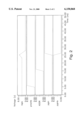
- FIG. 2 is a graph showing the simulated results of input/output signals in the anti-fuse programming circuit in FIG. 1.
- FIG. 1 is a circuit diagram showing the construction of an anti-fuse programming circuit which is applied to a memory device in accordance with an embodiment of the present invention.
- an operation switching part 10 is adapted to precharge the anti-fuse programming circuit with a half voltage HVCC to operate it. To this end, the operation switching part 10 is provided with a first PMOS transistor P1.
- the first PMOS transistor P1 has its source connected to the half voltage HVCC, its drain connected to one side of an anti-fuse 70 and its gate for inputting a complementary precharge signal prechb.
- a common connection point of the one side of the anti-fuse 70 and the drain of the first PMOS transistor P1 will be referred to hereinafter as a node ⁇ a ⁇ .
- a sense signal input part 20 includes an NMOS transistor N1 having its drain connected to the other side of the anti-fuse 70, its source connected to a ground voltage terminal and its gate for inputting a failed address signal ADDR.
- An output part 60 includes a first inverter INV1 for inverting a voltage level at the node a, and a second inverter INV2 for inverting an output signal from the first inverter INV1.
- the output repb of the second inverter INV2, or the output of the output part 60, is used to verify the programmed state of the anti-fuse 70. At a normal state, the output repb of the second inverter INV2 remains high in level.
- the first and second inverters INV1 and INV2 are operated by the half voltage HVCC, and the output repb of the output part 60 thus has the level of the half voltage HVCC when it is high in level.
- a breakdown voltage supply part 30 is operated in response to a complementary programming signal pgmb to supply a source voltage VCC to the node a. To this end, the breakdown voltage supply part 30 is provided with a second PMOS transistor P2.
- a current blocking part 40 is adapted to interrupt a breakdown voltage for the anti-fuse 70, or the source voltage VCC supplied from the breakdown voltage supply part 30 to block a current path from the breakdown voltage supply part 30 to the anti-fuse 70 after the anti-fuse 70 is programmed. To this end, the current blocking part 40 is provided with a third PMOS transistor P3.
- the second PMOS transistor P2 in the breakdown voltage supply part 30 has its source connected to the source voltage VCC, its drain connected to a source of the third PMOS transistor P3 in the current blocking part 40 and its gate for inputting the complementary programming signal pgmb.
- the third PMOS transistor P3 has its drain connected to the node a and its gate for inputting the output signal from the first inverter INV1 in the output part 60 fed back thereto, which inverts the voltage level at the node a.
- a latch part 50 is adapted to strongly stabilize the voltage level at the node a to prevent the output repb of the output part 60 from varying in level due to an instability of the half voltage HVCC applied to the node a at the normal state.
- the latch part 50 is provided with a fourth PMOS transistor P4 operated in response to the output signal from the first inverter INV1 in the output part 60 fed back thereto, which inverts the voltage level at the node a.
- the anti-fuse 70 is programmed under the condition that the failed address signal ADDR is inputted by the sense signal input part 50, the node a goes low in level, thereby causing the output of the first inverter INV1 to become high in level. As a result, the fourth PMOS transistor P4 in the latch part 50 is turned off to supply no further half voltage HVCC to the node a.
- FIG. 2 is a graph showing the simulated results of the input/output signals in the anti-fuse programming circuit in FIG. 1.
- a programming signal pgm is low in level and the complementary programming signal pgmb is high in level.
- the complementary precharge signal prechb goes low in level to precharge the anti-fuse programming circuit
- the fist PMOS transistor P1 in the operation switching part 10 is turned on to supply the half voltage HVCC to the node a.
- the anti-fuse programming circuit is precharged with the half voltage HVCC.
- the half voltage HVCC at the node a is inverted from high to low in level by the first inverter INV1 and again inverted from low to high in level by the second inverter INV2.
- the output repb of the output part 60 has a high voltage level which is the level of the half voltage HVCC.
- the low level output of the first inverter INV1 turns on the fourth PMOS transistor P4 in the latch part 50, thereby causing the fourth PMOS transistor P4 to supply the half voltage HVCC to the node a.
- the voltage level at the node a is strongly stabilized to prevent the output of the output part 60 from varying in level due to an instability of that voltage level.
- the low level output of the first inverter INV1 also turns on the third PMOS transistor P3 in the current blocking part 40, thereby allowing current from the breakdown voltage supply part 30 to flow through the third PMOS transistor P3 upon application of the program signal pgm.
- the complementary precharge signal prechb goes high in level under the above precharged condition, the first PMOS transistor P1 is turned off and the half voltage HVCC is thus not applied to the node a. At this time, the node a, however, remains precharged strongly with the half voltage HVCC by the latch part 50.
- the third PMOS transistor P3 in the current blocking part 40 remains on in response to the low level output of the first inverter INV1 fed back thereto.
- the NMOS transistor N1 is turned on. However, because there is no dielectric breakdown in the anti-fuse 70, the node a is not changed in voltage level, resulting in no variation in the output repb of the output part 60.
- the programming signal pgm goes high in level to program the anti-fuse 70
- the complementary programming signal pgmb becomes low in level.
- the second PMOS transistor P2 in the breakdown voltage supply part 30 is turned on to supply the source voltage VCC to the node a.
- a current path is formed from the node a to the ground voltage terminal through the anti-fuse 70 and the turned-on NMOS transistor N1, thus causing a dielectric breakdown in the anti-fuse 70.
- the node a is changed from high to low in level and then inverted from low to high in level by the first inverter INV1.
- the third PMOS transistor P3 in the current blocking part 40 is turned off to block the continuous supply of the source voltage VCC from the breakdown voltage supply part 30.
- the high level output of the first inverter INV1 also turns off the fourth PMOS transistor P4 in the latch part 50 so that the half voltage HVCC cannot further be supplied to the node a.
- the turned-off fourth PMOS transistor P4 functions to prevent the voltage level at the node a from being transferred to a half voltage HVCC terminal when it is the level of the source voltage VCC.
- the low level voltage at the node a is sequentially inverted by the first and second inverters INV1 and INV2, resulting in the output repb of the output part 60 becoming low in level. This indicates that the programmed state of the anti-fuse 70 is normal.
- the anti-fuse can be programmed in a dielectric breakdown manner at a package step of a semiconductor device to interconnect two electrodes. This results in improvements in unit cost and reliability.
- the anti-fuse is programmed in response to the anti-fuse programming signal, the programmed state thereof can be verified. Moreover, after a dielectric breakdown occurs in the anti-fuse, the continuous power supply thereto is blocked, resulting in a significant reduction in current consumption.
Landscapes
- For Increasing The Reliability Of Semiconductor Memories (AREA)
- Design And Manufacture Of Integrated Circuits (AREA)
- Techniques For Improving Reliability Of Storages (AREA)
- Fuses (AREA)
- Read Only Memory (AREA)
Abstract
Description
Claims (7)
Applications Claiming Priority (2)
| Application Number | Priority Date | Filing Date | Title |
|---|---|---|---|
| KR98-26226 | 1998-06-30 | ||
| KR1019980026226A KR100321169B1 (en) | 1998-06-30 | 1998-06-30 | Anti-fuse programming circuit |
Publications (1)
| Publication Number | Publication Date |
|---|---|
| US6150868A true US6150868A (en) | 2000-11-21 |
Family
ID=19542566
Family Applications (1)
| Application Number | Title | Priority Date | Filing Date |
|---|---|---|---|
| US09/342,600 Expired - Lifetime US6150868A (en) | 1998-06-30 | 1999-06-29 | Anti-fuse programming circuit |
Country Status (4)
| Country | Link |
|---|---|
| US (1) | US6150868A (en) |
| JP (1) | JP3665511B2 (en) |
| KR (1) | KR100321169B1 (en) |
| TW (1) | TW525059B (en) |
Cited By (23)
| Publication number | Priority date | Publication date | Assignee | Title |
|---|---|---|---|---|
| US6333667B2 (en) * | 1999-12-29 | 2001-12-25 | Hyundai Electronics Industries Co., Ltd. | Antifuse programming circuit |
| US6426668B1 (en) * | 2001-03-22 | 2002-07-30 | International Business Machines Corporation | Imbalanced sense amplifier fuse detection circuit |
| US6466498B2 (en) | 2001-01-10 | 2002-10-15 | Hewlett-Packard Company | Discontinuity-based memory cell sensing |
| US20020180511A1 (en) * | 2001-03-30 | 2002-12-05 | Intel Corporation | Externally programmable antifuse |
| US6570798B1 (en) * | 2000-12-20 | 2003-05-27 | Actel Corporation | Antifuse memory cell and antifuse memory cell array |
| US6594171B1 (en) | 2002-03-07 | 2003-07-15 | Hewlett-Packard Development Company, L.P. | Memory systems and methods of making the same |
| US20030218493A1 (en) * | 2002-05-27 | 2003-11-27 | Kang-Youl Lee | Antifuse Circuit |
| US6710640B1 (en) * | 2002-09-19 | 2004-03-23 | Infineon Technologies Ag | Active well-bias transistor for programming a fuse |
| US20040140835A1 (en) * | 2003-01-21 | 2004-07-22 | Gunther Lehmann | Multiple trip point fuse latch device and method |
| US20040213056A1 (en) * | 2003-03-31 | 2004-10-28 | Shiro Fujima | Redundancy control circuit which surely programs program elements and semiconductor memory using the same |
| US20040218328A1 (en) * | 2003-02-14 | 2004-11-04 | Naokazu Kuzuno | Fuse latch circuit |
| US6990010B1 (en) | 2003-08-06 | 2006-01-24 | Actel Corporation | Deglitching circuits for a radiation-hardened static random access memory based programmable architecture |
| FR2894373A1 (en) * | 2005-12-07 | 2007-06-08 | Atmel Corp | AUTONOMOUS ANTI-FUSE CELL |
| US20070171589A1 (en) * | 2006-01-20 | 2007-07-26 | Sanyo Electric Co., Ltd. | Zapping Circuit |
| US20080054988A1 (en) * | 2006-09-01 | 2008-03-06 | Etron Technology, Inc. | Fuse circuit |
| US7482854B2 (en) | 2005-04-26 | 2009-01-27 | Samsung Electronics Co., Ltd. | E-fuse circuit using leakage current path of transistor |
| US20090059682A1 (en) * | 2007-08-30 | 2009-03-05 | Bok-Gue Park | Semiconductor memory device having antifuse circuitry |
| US7502066B1 (en) | 2002-11-05 | 2009-03-10 | Foveon, Inc. | Methods for manufacturing and testing image sensing devices |
| US20100283504A1 (en) * | 2009-05-05 | 2010-11-11 | William Marsh Rice University | Method for fabrication of a semiconductor element and structure thereof |
| EP2849183A1 (en) * | 2013-09-17 | 2015-03-18 | Dialog Semiconductor GmbH | On-chip Voltage Generation for a Programmable Memory Device |
| US20170236666A1 (en) * | 2016-02-17 | 2017-08-17 | Dexerials Corporation | Protective element and protective circuit substrate using the same |
| US10255982B2 (en) | 2016-11-02 | 2019-04-09 | Skyworks Solutions, Inc. | Accidental fuse programming protection circuits |
| US10360988B2 (en) | 2016-11-02 | 2019-07-23 | Skyworks Solutions, Inc. | Apparatus and methods for protection against inadvertent programming of fuse cells |
Families Citing this family (8)
| Publication number | Priority date | Publication date | Assignee | Title |
|---|---|---|---|---|
| US6373771B1 (en) * | 2001-01-17 | 2002-04-16 | International Business Machines Corporation | Integrated fuse latch and shift register for efficient programming and fuse readout |
| JP3730932B2 (en) | 2002-04-16 | 2006-01-05 | エルピーダメモリ株式会社 | Semiconductor memory device and capacity fuse state confirmation method |
| JP4125542B2 (en) | 2002-05-20 | 2008-07-30 | エルピーダメモリ株式会社 | Semiconductor memory device and manufacturing method thereof |
| KR100865708B1 (en) * | 2002-07-19 | 2008-10-29 | 주식회사 하이닉스반도체 | Semiconductor deivce |
| JP2006268971A (en) | 2005-03-24 | 2006-10-05 | Elpida Memory Inc | Semiconductor memory device and its test method |
| KR100611309B1 (en) | 2005-06-29 | 2006-08-10 | 고려대학교 산학협력단 | Latch and flip-flop having the latch |
| KR100838372B1 (en) * | 2006-09-29 | 2008-06-13 | 주식회사 하이닉스반도체 | Semiconductor memory device for reducing power consumption |
| JP5302157B2 (en) * | 2009-10-05 | 2013-10-02 | ルネサスエレクトロニクス株式会社 | One-time programmable cell circuit and semiconductor integrated circuit having the same |
Citations (3)
| Publication number | Priority date | Publication date | Assignee | Title |
|---|---|---|---|---|
| US5448187A (en) * | 1992-11-18 | 1995-09-05 | Gemplus Card International | Antifuse programming method and circuit which supplies a steady current after a programming voltage has dropped |
| US5689455A (en) * | 1995-08-31 | 1997-11-18 | Micron Technology, Inc. | Circuit for programming antifuse bits |
| US5945840A (en) * | 1994-02-24 | 1999-08-31 | Micron Technology, Inc. | Low current redundancy anti-fuse assembly |
-
1998
- 1998-06-30 KR KR1019980026226A patent/KR100321169B1/en not_active IP Right Cessation
-
1999
- 1999-06-29 US US09/342,600 patent/US6150868A/en not_active Expired - Lifetime
- 1999-06-30 JP JP18533999A patent/JP3665511B2/en not_active Expired - Fee Related
- 1999-07-29 TW TW088112868A patent/TW525059B/en not_active IP Right Cessation
Patent Citations (3)
| Publication number | Priority date | Publication date | Assignee | Title |
|---|---|---|---|---|
| US5448187A (en) * | 1992-11-18 | 1995-09-05 | Gemplus Card International | Antifuse programming method and circuit which supplies a steady current after a programming voltage has dropped |
| US5945840A (en) * | 1994-02-24 | 1999-08-31 | Micron Technology, Inc. | Low current redundancy anti-fuse assembly |
| US5689455A (en) * | 1995-08-31 | 1997-11-18 | Micron Technology, Inc. | Circuit for programming antifuse bits |
Cited By (39)
| Publication number | Priority date | Publication date | Assignee | Title |
|---|---|---|---|---|
| US6333667B2 (en) * | 1999-12-29 | 2001-12-25 | Hyundai Electronics Industries Co., Ltd. | Antifuse programming circuit |
| US6570798B1 (en) * | 2000-12-20 | 2003-05-27 | Actel Corporation | Antifuse memory cell and antifuse memory cell array |
| US6466498B2 (en) | 2001-01-10 | 2002-10-15 | Hewlett-Packard Company | Discontinuity-based memory cell sensing |
| US6426668B1 (en) * | 2001-03-22 | 2002-07-30 | International Business Machines Corporation | Imbalanced sense amplifier fuse detection circuit |
| US6888398B2 (en) * | 2001-03-30 | 2005-05-03 | Intel Corporation | Externally programmable antifuse |
| US20020180511A1 (en) * | 2001-03-30 | 2002-12-05 | Intel Corporation | Externally programmable antifuse |
| US6594171B1 (en) | 2002-03-07 | 2003-07-15 | Hewlett-Packard Development Company, L.P. | Memory systems and methods of making the same |
| US20030218493A1 (en) * | 2002-05-27 | 2003-11-27 | Kang-Youl Lee | Antifuse Circuit |
| US6741117B2 (en) * | 2002-05-27 | 2004-05-25 | Hynix Semiconductor Inc. | Antifuse circuit |
| US6710640B1 (en) * | 2002-09-19 | 2004-03-23 | Infineon Technologies Ag | Active well-bias transistor for programming a fuse |
| US20040056703A1 (en) * | 2002-09-19 | 2004-03-25 | Chandrasekharan Kothandaraman | Active well-bias transistor for programming a fuse |
| US7502066B1 (en) | 2002-11-05 | 2009-03-10 | Foveon, Inc. | Methods for manufacturing and testing image sensing devices |
| US6882202B2 (en) | 2003-01-21 | 2005-04-19 | Infineon Technologies Ag | Multiple trip point fuse latch device and method |
| WO2004066309A1 (en) * | 2003-01-21 | 2004-08-05 | Infineon Technologies Ag | Multiple trip point fuse latch device and test method of the fuse |
| US20040140835A1 (en) * | 2003-01-21 | 2004-07-22 | Gunther Lehmann | Multiple trip point fuse latch device and method |
| US7260012B2 (en) * | 2003-02-14 | 2007-08-21 | Kabushiki Kaisha Toshiba | Fuse latch circuit |
| US20040218328A1 (en) * | 2003-02-14 | 2004-11-04 | Naokazu Kuzuno | Fuse latch circuit |
| US20040213056A1 (en) * | 2003-03-31 | 2004-10-28 | Shiro Fujima | Redundancy control circuit which surely programs program elements and semiconductor memory using the same |
| US7075835B2 (en) | 2003-03-31 | 2006-07-11 | Elpida Memory, Inc. | Redundancy control circuit which surely programs program elements and semiconductor memory using the same |
| US20080298116A1 (en) * | 2003-08-06 | 2008-12-04 | Actel Corporation | Deglitching circuits for a radiation-hardened static random access memory based programmable architecture |
| US6990010B1 (en) | 2003-08-06 | 2006-01-24 | Actel Corporation | Deglitching circuits for a radiation-hardened static random access memory based programmable architecture |
| US7126842B2 (en) | 2003-08-06 | 2006-10-24 | Actel Corporation | Deglitching circuits for a radiation-hardened static random access memory based programmable architecture |
| US7672153B2 (en) | 2003-08-06 | 2010-03-02 | Actel Corporation | Deglitching circuits for a radiation-hardened static random access memory based programmable architecture |
| US20060126376A1 (en) * | 2003-08-06 | 2006-06-15 | Actel Corporation | Deglitching circuits for a radiation-hardened static random access memory based programmable architecture |
| US7482854B2 (en) | 2005-04-26 | 2009-01-27 | Samsung Electronics Co., Ltd. | E-fuse circuit using leakage current path of transistor |
| FR2894373A1 (en) * | 2005-12-07 | 2007-06-08 | Atmel Corp | AUTONOMOUS ANTI-FUSE CELL |
| US20070171589A1 (en) * | 2006-01-20 | 2007-07-26 | Sanyo Electric Co., Ltd. | Zapping Circuit |
| US7525368B2 (en) * | 2006-09-01 | 2009-04-28 | Etron Technology, Inc. | Fuse circuit |
| US20080054988A1 (en) * | 2006-09-01 | 2008-03-06 | Etron Technology, Inc. | Fuse circuit |
| US20090059682A1 (en) * | 2007-08-30 | 2009-03-05 | Bok-Gue Park | Semiconductor memory device having antifuse circuitry |
| US20100283504A1 (en) * | 2009-05-05 | 2010-11-11 | William Marsh Rice University | Method for fabrication of a semiconductor element and structure thereof |
| US7973559B2 (en) * | 2009-05-05 | 2011-07-05 | William Marsh Rice University | Method for fabrication of a semiconductor element and structure thereof |
| EP2849183A1 (en) * | 2013-09-17 | 2015-03-18 | Dialog Semiconductor GmbH | On-chip Voltage Generation for a Programmable Memory Device |
| US9263097B2 (en) | 2013-09-17 | 2016-02-16 | Dialog Semiconductor Gmbh | On-chip voltage generation for a programmable memory device |
| US20170236666A1 (en) * | 2016-02-17 | 2017-08-17 | Dexerials Corporation | Protective element and protective circuit substrate using the same |
| US9870886B2 (en) * | 2016-02-17 | 2018-01-16 | Dexerials Corporation | Protective element and protective circuit substrate using the same |
| US10255982B2 (en) | 2016-11-02 | 2019-04-09 | Skyworks Solutions, Inc. | Accidental fuse programming protection circuits |
| US10360988B2 (en) | 2016-11-02 | 2019-07-23 | Skyworks Solutions, Inc. | Apparatus and methods for protection against inadvertent programming of fuse cells |
| US10643727B2 (en) | 2016-11-02 | 2020-05-05 | Skyworks Solutions, Inc. | Apparatus and methods for protection against inadvertent programming of fuse cells |
Also Published As
| Publication number | Publication date |
|---|---|
| JP2000090689A (en) | 2000-03-31 |
| JP3665511B2 (en) | 2005-06-29 |
| KR20000004730A (en) | 2000-01-25 |
| TW525059B (en) | 2003-03-21 |
| KR100321169B1 (en) | 2002-05-13 |
Similar Documents
| Publication | Publication Date | Title |
|---|---|---|
| US6150868A (en) | Anti-fuse programming circuit | |
| US6144247A (en) | Anti-fuse programming circuit using variable voltage generator | |
| US6108261A (en) | Repair circuit for redundancy circuit with anti-fuse | |
| US5566107A (en) | Programmable circuit for enabling an associated circuit | |
| KR100504433B1 (en) | Repair circuit of memory device used anti-fuse | |
| JPH08321197A (en) | Semiconductor memory element | |
| US6133778A (en) | Anti-fuse programming circuit with cross-coupled feedback loop | |
| JPH08330944A (en) | Semiconductor device | |
| US5825698A (en) | Redundancy decoding circuit for a semiconductor memory device | |
| US7116127B2 (en) | Circuit with fuse and semiconductor device having the same circuit | |
| KR100673002B1 (en) | EFUSE circuit using leakage current path of transistor | |
| KR100560343B1 (en) | Fuse circuit having zero power draw for partially blown condition | |
| KR19990057343A (en) | Antifuse Stabilization Circuit | |
| US6236241B1 (en) | Redundant decoder having fuse-controlled transistor | |
| KR100646575B1 (en) | Method of programming fuse for repairing semiconductor memory device and circuit for verifying success of fuse programming | |
| US6888216B2 (en) | Circuit having make-link type fuse and semiconductor device having the same | |
| KR20010008398A (en) | Internal voltage generator having anti-fuse | |
| JPH038039B2 (en) | ||
| KR100341579B1 (en) | Repair device of semiconductor memory device | |
| KR20000003602A (en) | Inner voltage generating circuit | |
| KR20060039483A (en) | Method of detecting programmed fuse and programmed fuse detecting circuit for the same | |
| KR20020074574A (en) | Repair circuit for memory device of semiconductor | |
| KR20010004003A (en) | Repair fuse circuit |
Legal Events
| Date | Code | Title | Description |
|---|---|---|---|
| AS | Assignment |
Owner name: HYUNDAI ELECTRONICS INDUSTRIES CO., LTD., KOREA, R Free format text: ASSIGNMENT OF ASSIGNORS INTEREST;ASSIGNORS:KIM, YOUNG-HEE;KU, KIE-BONG;REEL/FRAME:010257/0807 Effective date: 19990714 |
|
| STCF | Information on status: patent grant |
Free format text: PATENTED CASE |
|
| FEPP | Fee payment procedure |
Free format text: PAYOR NUMBER ASSIGNED (ORIGINAL EVENT CODE: ASPN); ENTITY STATUS OF PATENT OWNER: LARGE ENTITY |
|
| FPAY | Fee payment |
Year of fee payment: 4 |
|
| FPAY | Fee payment |
Year of fee payment: 8 |
|
| FEPP | Fee payment procedure |
Free format text: PAYOR NUMBER ASSIGNED (ORIGINAL EVENT CODE: ASPN); ENTITY STATUS OF PATENT OWNER: LARGE ENTITY Free format text: PAYER NUMBER DE-ASSIGNED (ORIGINAL EVENT CODE: RMPN); ENTITY STATUS OF PATENT OWNER: LARGE ENTITY |
|
| FPAY | Fee payment |
Year of fee payment: 12 |