US6073343A - Method of providing a variable guard ring width between detectors on a substrate - Google Patents
Method of providing a variable guard ring width between detectors on a substrate Download PDFInfo
- Publication number
- US6073343A US6073343A US09/218,259 US21825998A US6073343A US 6073343 A US6073343 A US 6073343A US 21825998 A US21825998 A US 21825998A US 6073343 A US6073343 A US 6073343A
- Authority
- US
- United States
- Prior art keywords
- guard ring
- detectors
- ring width
- substrate
- maximizing
- Prior art date
- Legal status (The legal status is an assumption and is not a legal conclusion. Google has not performed a legal analysis and makes no representation as to the accuracy of the status listed.)
- Expired - Fee Related
Links
- 239000000758 substrate Substances 0.000 title claims abstract description 55
- 238000000034 method Methods 0.000 title claims abstract description 23
- 238000004519 manufacturing process Methods 0.000 claims abstract description 6
- 239000010410 layer Substances 0.000 claims description 114
- 239000004020 conductor Substances 0.000 claims description 25
- 239000012811 non-conductive material Substances 0.000 claims description 25
- 239000002356 single layer Substances 0.000 claims description 3
- 239000000463 material Substances 0.000 description 6
- 238000013461 design Methods 0.000 description 5
- 230000036961 partial effect Effects 0.000 description 5
- 238000000926 separation method Methods 0.000 description 4
- 230000008901 benefit Effects 0.000 description 3
- 230000015572 biosynthetic process Effects 0.000 description 3
- 238000005755 formation reaction Methods 0.000 description 3
- 230000002411 adverse Effects 0.000 description 2
- 239000003989 dielectric material Substances 0.000 description 2
- 239000011521 glass Substances 0.000 description 2
- 229910052581 Si3N4 Inorganic materials 0.000 description 1
- VYPSYNLAJGMNEJ-UHFFFAOYSA-N Silicium dioxide Chemical compound O=[Si]=O VYPSYNLAJGMNEJ-UHFFFAOYSA-N 0.000 description 1
- 229910052782 aluminium Inorganic materials 0.000 description 1
- 239000007795 chemical reaction product Substances 0.000 description 1
- 229910052804 chromium Inorganic materials 0.000 description 1
- 230000007797 corrosion Effects 0.000 description 1
- 238000005260 corrosion Methods 0.000 description 1
- 230000003247 decreasing effect Effects 0.000 description 1
- 230000000670 limiting effect Effects 0.000 description 1
- 239000002184 metal Substances 0.000 description 1
- 229910052751 metal Inorganic materials 0.000 description 1
- 238000012986 modification Methods 0.000 description 1
- 230000004048 modification Effects 0.000 description 1
- 229910052750 molybdenum Inorganic materials 0.000 description 1
- 238000012545 processing Methods 0.000 description 1
- 230000002829 reductive effect Effects 0.000 description 1
- 230000001172 regenerating effect Effects 0.000 description 1
- 230000035945 sensitivity Effects 0.000 description 1
- HQVNEWCFYHHQES-UHFFFAOYSA-N silicon nitride Chemical compound N12[Si]34N5[Si]62N3[Si]51N64 HQVNEWCFYHHQES-UHFFFAOYSA-N 0.000 description 1
- 229910052814 silicon oxide Inorganic materials 0.000 description 1
- 229910052715 tantalum Inorganic materials 0.000 description 1
- 238000012360 testing method Methods 0.000 description 1
- 229910052719 titanium Inorganic materials 0.000 description 1
- 229910052721 tungsten Inorganic materials 0.000 description 1
Images


Classifications
-
- H—ELECTRICITY
- H01—ELECTRIC ELEMENTS
- H01L—SEMICONDUCTOR DEVICES NOT COVERED BY CLASS H10
- H01L31/00—Semiconductor devices sensitive to infrared radiation, light, electromagnetic radiation of shorter wavelength or corpuscular radiation and specially adapted either for the conversion of the energy of such radiation into electrical energy or for the control of electrical energy by such radiation; Processes or apparatus specially adapted for the manufacture or treatment thereof or of parts thereof; Details thereof
- H01L31/02—Details
- H01L31/02002—Arrangements for conducting electric current to or from the device in operations
-
- H—ELECTRICITY
- H01—ELECTRIC ELEMENTS
- H01L—SEMICONDUCTOR DEVICES NOT COVERED BY CLASS H10
- H01L27/00—Devices consisting of a plurality of semiconductor or other solid-state components formed in or on a common substrate
- H01L27/02—Devices consisting of a plurality of semiconductor or other solid-state components formed in or on a common substrate including semiconductor components specially adapted for rectifying, oscillating, amplifying or switching and having at least one potential-jump barrier or surface barrier; including integrated passive circuit elements with at least one potential-jump barrier or surface barrier
- H01L27/0203—Particular design considerations for integrated circuits
- H01L27/0248—Particular design considerations for integrated circuits for electrical or thermal protection, e.g. electrostatic discharge [ESD] protection
-
- H—ELECTRICITY
- H01—ELECTRIC ELEMENTS
- H01L—SEMICONDUCTOR DEVICES NOT COVERED BY CLASS H10
- H01L27/00—Devices consisting of a plurality of semiconductor or other solid-state components formed in or on a common substrate
- H01L27/14—Devices consisting of a plurality of semiconductor or other solid-state components formed in or on a common substrate including semiconductor components sensitive to infrared radiation, light, electromagnetic radiation of shorter wavelength or corpuscular radiation and specially adapted either for the conversion of the energy of such radiation into electrical energy or for the control of electrical energy by such radiation
- H01L27/144—Devices controlled by radiation
- H01L27/146—Imager structures
- H01L27/14601—Structural or functional details thereof
-
- Y—GENERAL TAGGING OF NEW TECHNOLOGICAL DEVELOPMENTS; GENERAL TAGGING OF CROSS-SECTIONAL TECHNOLOGIES SPANNING OVER SEVERAL SECTIONS OF THE IPC; TECHNICAL SUBJECTS COVERED BY FORMER USPC CROSS-REFERENCE ART COLLECTIONS [XRACs] AND DIGESTS
- Y10—TECHNICAL SUBJECTS COVERED BY FORMER USPC
- Y10T—TECHNICAL SUBJECTS COVERED BY FORMER US CLASSIFICATION
- Y10T29/00—Metal working
- Y10T29/49—Method of mechanical manufacture
- Y10T29/49002—Electrical device making
- Y10T29/49117—Conductor or circuit manufacturing
Landscapes
- Engineering & Computer Science (AREA)
- Power Engineering (AREA)
- Physics & Mathematics (AREA)
- Condensed Matter Physics & Semiconductors (AREA)
- General Physics & Mathematics (AREA)
- Computer Hardware Design (AREA)
- Microelectronics & Electronic Packaging (AREA)
- Electromagnetism (AREA)
- Solid State Image Pick-Up Elements (AREA)
- Devices For Indicating Variable Information By Combining Individual Elements (AREA)
Abstract
A method is provided for maximizing substrate usage in the fabrication of flat panel displays or detectors, while also maximizing electrostatic protection for the displays or detectors. Initially, at least two detectors are positioned on the substrate, with each of the detectors having a guard ring of a certain width. At least a section of the guard ring width of one detector is approximately adjacent to a section of the guard ring width of another detector. The approximately adjacent guard ring width sections are then positioned such that a maximum overlap of the adjacent guard ring width sections is achieved, while still providing each display or detector with electrostatic discharge protection. Each of the detectors is separated from the other detectors and the remainder of the substrate by the process of scribing partially through the substrate and breaking at the scribe mark or by sawing.
Description
The present invention relates to detectors or displays fabricated on substrates, typically glass, in particular balancing the minimization of size of the detector (x-ray or light) or display (hereinafter generally referred to as detector), thereby maximizing the usage of the substrate area, and maximizing the electrostatic discharge protection afforded by the guard ring; an area of conductive material formed as part of each detector perimeter on a single substrate. A wider guard ring provides more protection, while decreasing the remaining area of the substrate available to form additional detectors.
Detectors are replicated on a single insulating substrate (i.e., glass) during fabrication, using a sequence of photomasks and associated processing, as is well known in the art. Detectors on the substrate are separated from one another by the guard ring of each of the detectors. Near the end of the fabrication process, the substrate is scribed and the individual detectors are separated from one another. The detector is comprised of the active area, which is in turn comprised of individual picture elements (or pixels), contact fingers located on the periphery on one or more sides of the active area, and the guard ring. The guard ring forms a perimeter around both the contact fingers and the active area.
The guard ring may be comprised of one or more materials, at least one of which will be conductive. Because the devices which comprise the pixels in the active area are very sensitive to electrostatic discharge (ESD), which may alter their function or destroy them altogether, they must be protected from discharge, particularly during and after separation when the detectors are subject to ESD from handling. The guard ring affords some protection in that its width forms a gap between the edge of the detector which is handled and the contact fingers which form part of a very conductive path directly into the sensitive active area of the detector. Furthermore, the guard ring can be contacted to a known potential (ground, for example) during the fabrication and detector assembly steps which occur after separation (test, for example) and when it is assembled to the associated support electronics in the intended end product. This will further reduce the chance that ESD will damage the devices comprising part of the pixels. Contacting the guard ring to a known potential also indicates the guard ring should be conductive.
The ESD sensitivity of the devices forming part of the pixels in the active area often can not be predicted before they are first fabricated. A device which is very sensitive to ESD will benefit from more protection (i.e., a wider guard ring). The optimum guard ring width cannot be determined during the initial design, meaning that the design, including the sensitive devices and the guard ring width, must be fabricated and tested before the guard ring width can be evaluated. This implies that the final design will be generated only after one or more design iterations have been fabricated and tested. This further implies that the time to complete the design is increased as is the cost of generating additional iterations of the photomasks in order to optimize the guard ring width. A photolithographic exposure tool may be used to position each guard ring. Lastly, the guard ring width cannot be made arbitrarily large because for smaller detectors fabricated on larger substrates, this would imply fewer detectors per substrate are produced, which also would adversely affect cost.
It would be desirable, then, to have a means for providing a variable guard ring width between detectors on a substrate, which guard ring width can be varied for the purpose of experimentally determining the optimal width for ESD protection without the time and expense associated with regenerating the photomasks.
In accordance with the present invention, the effective guard ring width for an individual detector can be varied over a factor of two, by choosing the amount each detector is overlapped during the fabrication process. At the extremes, the guard rings of adjacent detectors would be either totally overlapped or abutted edge to edge, with the latter arrangement providing twice the guard ring width as the former arrangement, ignoring any material lost during separation. With the present invention, any amount of overlap between the extremes is also achievable.
In accordance with one aspect of the present invention, a method for maximizing substrate usage, comprises the step of providing at least two detectors on the substrate, the two detectors each having a guard ring, and the guard rings of the two detectors arranged such that the guard rings are approximately adjacent. The approximately adjacent guard rings are then positioned such that a maximum overlap is achieved which provides minimum ESD protection.
Accordingly, it is an object of the present invention to provide a variable guard ring width. This has the advantages of allowing detector dimensions to be minimized, thereby maximizing substrate usage, while still providing sufficient ESD protection to the detector.
Other objects and advantages of the invention will be apparent from the following description, the accompanying drawings and the appended claims.
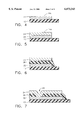
FIG. 1 illustrates two single detectors with abutted guard rings, on a single substrate;
FIG. 2 illustrates two single detectors with 100% overlap of adjacent guard rings;
FIG. 3 illustrates two single detectors with the adjacent guard rings partially overlapped;
FIG. 4 illustrates a guard ring embodiment wherein the guard ring is comprised of a single layer of conductive material;
FIG. 5 illustrates another guard ring embodiment wherein the guard ring is comprised of two different layers of conductive material;
FIG. 6 illustrates yet another embodiment wherein the guard ring is comprised of two different layers of conductive material separated by one layer of non-conductive material;
FIG. 7 illustrates yet another alternative embodiment wherein the guard ring is comprised of two different layers of conductive material separated by one layer of non-conductive material in only part of the guard ring, and with a conductive path established between the two layers of conductive material in the remaining part of the guard ring; and
FIGS. 8-17 illustrate additional embodiments of the present invention, to provide for more than two conductive layers, more than one dielectric, and more than one via formed between the various conductive layers.
In accordance with the present invention, the goal of maximizing substrate usage is balanced against the goal of using the guard ring to provide ESD protection. It is accepted in the art that maximum guard ring width will give maximum ESD protection; nevertheless, minimal guard ring width will give maximum substrate usage. The present invention, therefore, maximizes substrate usage by minimizing detector size; minimizes detector size by minimizing guard ring width; yet still provides the opportunity to improve ESD protection without generating new photomasks.
Referring now to the drawings, the concept of the present invention is illustrated. In FIG. 1, two detectors 10 and 12 on a single substrate 13 each have a guard ring 14, typically metal and therefore capable of providing at least some ESD protection. The width of guard ring 14 is in the range from about 0.5 mm to about 10 cm. Adjacent guard ring width portions 14a of each detector are abutted at line 16, but not overlapped. Such an arrangement, while maximizing ESD protection, has the disadvantage of also maximizing detector 10 and 12 size. If a plurality of detectors are arranged on a single substrate, with adjacent guard rings all abutted and never overlapped, the substrate usage is disadvantageously minimized, because the maximum size of the imager active area is limited.
This particular problem of substrate usage can be corrected by the configuration of FIG. 2, wherein adjacent guard ring width portions 14a of die 10 and 12 are totally overlapped, as indicated by overlap section 18. However, the ESD protection provided by such a configuration is necessarily reduced, as compared to the configuration of FIG. 1. Of course, it will be understood by those skilled in the art that certain applications of detectors may achieve the goal of maximizing substrate usage with the 100% percent overlap, without adversely compromising the ESD protection. Conversely, it will also be understood by those skilled in the art that certain applications of detectors may only be able to achieve the goal of sufficient ESD protection by abutting, but not overlapping, guard rings, as shown in FIG. 1.
In accordance with the present invention, sufficient ESD protection can often be provided with partial guard ring width overlap. That is, the goals of maximizing both substrate usage and ESD protection can be achieved without requiring either the complete non-overlap of FIG. 1, or the 100% overlap of FIG. 2. Partial overlap section 20, illustrating a partial overlap of adjacent guard ring width sections 14a, is shown in FIG. 3. Of course, it will be understood by those skilled in the art that the amount of partial overlap can vary, and the amount of partial overlap illustrated in FIG. 3 is not to be considered as limiting the variable guard ring width concept of the present invention.
At the extremes then as illustrated in FIGS. 1 and 2, the guard rings 14a of adjacent detector 10 and 12 can be either abutted edge to edge (FIG. 1) or totally overlapped (FIG. 2), with the former arrangement providing twice the guard ring width as the latter arrangement, ignoring any material lost during separation. With the present invention, any amount of overlap between the extremes (FIG. 3), in addition to the extremes, is also achievable, all without necessitating the generation of additional photomasks.
The guard ring referred to throughout this discussion may be formed in more than one manner. The most simple embodiment would be that of a single layer of conductive material (referred to as conductive layer 22). FIG. 4 is a representation of a cross section of the right edge of the guard ring width portion 14a of detector 12 and substrate 13 from FIG. 1.
FIG. 5 is a representation of the same area shown in FIG. 4 except that the guard ring is formed by two layers of conductive material, shown as first conductive layer 22 and second conductive layer 24. The conducting layers may comprise, for example, Mo, Al, Cr, Ta, Ti, W and ITO, or any multilayer combination of these or similar materials, with thicknesses typically from about 0.05 micron to 1.0 micron. Each conductive layer can be multilayer.
FIG. 6 illustrates yet another embodiment wherein the guard ring is comprised of two different layers of conductive material 22 and 24 separated by one layer of non-conductive material 26.
FIG. 7 is a representation of the same area as shown in FIG. 4 with a guard ring formed by two layers of conductive material, i.e., conductive layers 22 and 24. The non-conductive material may comprise inorganic dielectrics such as silicon oxide or silicon nitride, or organic dielectrics such as polymide, or a multilayer combination of these materials, with thicknesses typically from about 0.1 micron to 2 microns. The conductive layers 22 and 24 are separated by a non-conductive material 26 in the guard ring area with a conductive path, commonly referred to as a via 28, between conductive layer 22 and conductive layer 24. The via 28 displaces non-conductive material 26 in portions of the guard ring for the purpose of establishing a conductive path between first and second conductive layers 22 and 24. The via is filled with the same material and at the same time as the second conductive layer 24, due largely to the absence of non-conductive material 26 in certain areas of the guard ring.
FIG. 8 is a representation of the same area as shown in FIG. 4, with a guard ring formed by three layers of conductive material (first conductive layer 22, second conductive layer 24, and third conductive layer 32).
FIG. 9 is also a representation of the same area as shown in FIG. 4, with a guard ring formed by three layers of conductive material (first conductive layer 22, second conductive layer 24, and third conductive layer 32), with the second conductive layer 24 separated from the third conductive layer 32 in the guard ring area by a layer of non-conductive material 26.
FIG. 10 again is a representation of the same area as shown in FIG. 4, with a guard ring formed by three layers of conductive material (first conductive layer 22, second conductive layer 24, and third conductive layer 32), with the first conductive layer 22 separated from the second conductive layer 24 in the guard ring area by a layer of non-conductive material 26.
FIG. 11 is also a representation of the same area as shown in FIG. 4, with a guard ring formed by three layers of conductive material (first conductive layer 22, second conductive layer 24, and third conductive layer 32). In this embodiment, the first conductive layer 22 is separated by a layer of non-conductive material 26 from the second conductive layer 24, which in turn is separated by a layer of non-conductive material 30 from the third conductive layer 32.
FIG. 12 is a representation of the same area as shown in FIG. 4, with a guard ring formed by three layers of conductive material (first conductive layer 22, second conductive layer 24, and third conductive layer 32). The second conductive layer 24 is separated by a layer of non-conductive material 26 from third conductive layer 32, except in the area of via 28.
FIG. 13 is also a representation of the same area as shown in FIG. 4, with a guard ring formed by three layers of conductive material (first conductive layer 22, second conductive layer 24, and third conductive layer 32), with first conductive layer 22 separated by a layer of non-conductive material 26 from second conductive layer 24, except in the area of via 28.
FIG. 14 is, again, a representation of the same area as shown in FIG. 4. In FIG. 14, the guard ring is formed by three layers of conductive material (first conductive layer 22, second conductive layer 24, and third conductive layer 32). The first conductive layer 22 is separated, by a layer of non-conductive material 26, from second conductive layer 24, except in the area of via 28. Also, the second conductive layer 24 is separated, by a layer of non-conductive material 30, from the third conductive layer 32.
FIG. 15 is yet another representation of the same area as shown in FIG. 4, with a guard ring again formed by three layers of conductive material (first conductive layer 22, second conductive layer 24, and third conductive layer 32). In this embodiment, first conductive layer 22 is separated by a layer of non-conductive material 26 from second conductive layer 24. In addition, second conductive layer 24 is separated by a layer of non-conductive material 30 from third conductive layer 32, except in the area of via 28.
FIG. 16 is yet another embodiment of the same area as shown in FIG. 4, again with a guard ring formed by three layers of conductive material (first conductive layer 22, second conductive layer 24, and third conductive layer 32). In the embodiment of FIG. 16, first conductive layer 22 is separated by a layer of non-conductive material 26 from second conductive layer 24, except in the area of via 28. Furthermore, second conductive layer 24 is separated by a layer of non-conductive material 30 from third conductive layer 32, except in the area of via 28.
Yet another embodiment of the present invention, shown in FIG. 17, is a representation of the same area as shown in FIG. 4. In FIG. 17, the guard ring is again formed by three layers of conductive material (first conductive layer 22, second conductive layer 24, and third conductive layer 32). The first conductive layer 22 is separated by a layer of non-conductive material 26 from second conductive layer 24, except in the area of via 28. The second conductive layer 24 is separated by a layer of non-conductive material 30 from the third conductive layer 32, except in the area of a second via 34.
The present invention maximizes substrate usage. This is accomplished as described above, with the positioning of the detectors and guard ring width sections. Furthermore, a photolithographic exposure tool can be used to position each detector. Substrate usage can further be maximized by scribing partially through the substrate to define a scribed area and breaking, or sawing, the substrate at the scribed area to separate each of the detectors from every other detector.
As will be recognized by those skilled in the art, the formation of the guard ring is not limited to those formations discussed herein. Corrosion resistant imagers are described and claimed in co-pending patent application Ser. No. 08/996,250, incorporated herein by reference. The guard ring may be one of the many different formations known in the art, in particular, with three conductive layers, and up to two dielectric layers with up to two vias between conductive layers.
The invention has been described in detail with particular reference to certain preferred embodiments thereof, but it will be understood that modifications and variations can be effected within the spirit and scope of the invention.
Claims (18)
1. A method for maximizing substrate usage in the fabrication of flat panel displays or detectors, comprising the steps of:
providing at least two detectors on the substrate, the two detectors each having a guard ring width;
arranging at least a section of the guard ring width of each of the at least two detectors to be approximately adjacent;
positioning the approximately adjacent guard ring width sections such that edge sections of the adjacent guard ring width sections at least contact while providing each display or detector with electrostatic discharge protection, wherein each of the at least two detectors is separated from every other of the at least two detectors.
2. A method for maximizing substrate usage as claimed in claim 1 wherein the step of positioning the approximately adjacent guard ring width sections comprises the step of partially overlapping the approximately adjacent guard ring width sections.
3. A method for maximizing substrate usage as claimed in claim 1 wherein the step of positioning the approximately adjacent guard ring width sections comprises the step of fully overlapping one approximately adjacent guard ring width section over an other approximately adjacent guard ring width section.
4. A method for maximizing substrate usage as claimed in claim 1 wherein the step of positioning the approximately adjacent guard ring width sections comprises the step of abutting an edge section of one approximately adjacent guard ring width section with an edge sections of another approximately adjacent guard ring width section.
5. A method for maximizing substrate usage as claimed in claim 1 wherein the guard ring width is from about 0.5 mm to about 10 cm.
6. A method for maximizing substrate usage as claimed in claim 1 further comprising the steps of:
scribing partially through the substrate to define a scribed area; and
breaking the substrate at the scribed area to separate each of the at least two detectors from every other of the at least two detectors.
7. A method for maximizing substrate usage as claimed in claim 6 further comprising the step of sawing the substrate to separate each of the at least two detectors from every other of the at least two detectors.
8. A method for maximizing substrate usage as claimed in claim 1 further comprising the step of using a photolithographic exposure tool to position each detector.
9. A method for maximizing substrate usage as claimed in claim 1 further comprising the steps of:
forming each guard ring with a single layer of conductive material; and
separating each of the at least two detectors from every other of the at least two detectors.
10. A method for maximizing substrate usage as claimed in claim 1 further comprising the step of forming the guard ring of multiple layers of conductive material.
11. A method for maximizing substrate usage as claimed in claim 10 further comprising the step of applying at least one non-conductive material layer to separate at least two adjacent conductive layers.
12. A method for maximizing substrate usage as claimed in claim 11 further comprising the step of providing at least one via formed in at least one of the conductive or non-conductive material layers.
13. As claimed in claim 12 whereby the at least one non-conductive material layer separates adjacent conductive material layers, except at the at least one via.
14. A method for maximizing substrate usage as claimed in claim 1 further comprising the step of forming the guard ring of a first and second conductive material interposed with a layer of non-conductive material, whereby the first and second conductive layers lack a conductive path.
15. A method for maximizing substrate usage, comprising the steps of:
providing at least two detectors, the at least two detectors each having a guard ring width; and
positioning the at least two detectors to minimize detector size by overlapping at least a portion of the guard ring width of one of the at least two detectors with at least a portion of the guard ring width of another of the at least two detectors.
16. A method for maximizing substrate usage as claimed in claim 15 wherein the step of positioning comprises the step of fully overlapping a guard ring width of one detector with an adjacent guard ring width of another detector.
17. A method for maximizing substrate usage as claimed in claim 15 wherein the step of positioning comprises the step of partially overlapping a guard ring width of one detector with an adjacent guard ring width of another detector.
18. A method for maximizing substrate usage as claimed in claim 15 further comprising the step of providing electrostatic discharge protection for the substrate.
Priority Applications (3)
| Application Number | Priority Date | Filing Date | Title |
|---|---|---|---|
| US09/218,259 US6073343A (en) | 1998-12-22 | 1998-12-22 | Method of providing a variable guard ring width between detectors on a substrate |
| JP11338989A JP2000307093A (en) | 1998-12-22 | 1999-11-30 | Method of maximizing substrate usage |
| FR9916294A FR2787638B1 (en) | 1998-12-22 | 1999-12-22 | METHOD OF OPTIMIZING THE USE OF A SUBSTRATE IN THE MANUFACTURE OF PANEL DISPLAYS OR DETECTORS |
Applications Claiming Priority (1)
| Application Number | Priority Date | Filing Date | Title |
|---|---|---|---|
| US09/218,259 US6073343A (en) | 1998-12-22 | 1998-12-22 | Method of providing a variable guard ring width between detectors on a substrate |
Publications (1)
| Publication Number | Publication Date |
|---|---|
| US6073343A true US6073343A (en) | 2000-06-13 |
Family
ID=22814398
Family Applications (1)
| Application Number | Title | Priority Date | Filing Date |
|---|---|---|---|
| US09/218,259 Expired - Fee Related US6073343A (en) | 1998-12-22 | 1998-12-22 | Method of providing a variable guard ring width between detectors on a substrate |
Country Status (3)
| Country | Link |
|---|---|
| US (1) | US6073343A (en) |
| JP (1) | JP2000307093A (en) |
| FR (1) | FR2787638B1 (en) |
Cited By (51)
| Publication number | Priority date | Publication date | Assignee | Title |
|---|---|---|---|---|
| US20040120453A1 (en) * | 2002-12-23 | 2004-06-24 | Habib Vafi | Methods and apparatus for X-ray image detector assemblies |
| WO2004066194A1 (en) * | 2003-01-22 | 2004-08-05 | Nokia Corporation | Improved sensing arrangement |
| US20040268284A1 (en) * | 2003-06-24 | 2004-12-30 | International Business Machines Corporation | Method of forming guard ring parameterized cell structure in a hierarchical parameterized cell design, checking and verification system |
| US20050244039A1 (en) * | 2004-04-23 | 2005-11-03 | Validity Sensors, Inc. | Methods and apparatus for acquiring a swiped fingerprint image |
| US20080304246A1 (en) * | 2007-06-07 | 2008-12-11 | Ge Medical Systems Global Technology Company, Llc | Emi shielding of digital x-ray detectors with non-metallic enclosures |
| US20090252386A1 (en) * | 2008-04-04 | 2009-10-08 | Validity Sensors, Inc. | Apparatus and Method for Reducing Parasitic Capacitive Coupling and Noise in Fingerprint Sensing Circuits |
| US20100060757A1 (en) * | 2006-12-11 | 2010-03-11 | Fujifilm Corporation | Solid-state image pickup device |
| US20110045632A1 (en) * | 2002-09-20 | 2011-02-24 | Canon Kabushiki Kaisha | Methods of Manufacturing Solid State Image Pickup Devices |
| US8107212B2 (en) | 2007-04-30 | 2012-01-31 | Validity Sensors, Inc. | Apparatus and method for protecting fingerprint sensing circuitry from electrostatic discharge |
| US8116540B2 (en) | 2008-04-04 | 2012-02-14 | Validity Sensors, Inc. | Apparatus and method for reducing noise in fingerprint sensing circuits |
| US8131026B2 (en) | 2004-04-16 | 2012-03-06 | Validity Sensors, Inc. | Method and apparatus for fingerprint image reconstruction |
| US8165355B2 (en) | 2006-09-11 | 2012-04-24 | Validity Sensors, Inc. | Method and apparatus for fingerprint motion tracking using an in-line array for use in navigation applications |
| US8175345B2 (en) | 2004-04-16 | 2012-05-08 | Validity Sensors, Inc. | Unitized ergonomic two-dimensional fingerprint motion tracking device and method |
| US8204281B2 (en) | 2007-12-14 | 2012-06-19 | Validity Sensors, Inc. | System and method to remove artifacts from fingerprint sensor scans |
| US8224044B2 (en) | 2004-10-04 | 2012-07-17 | Validity Sensors, Inc. | Fingerprint sensing assemblies and methods of making |
| US8229184B2 (en) | 2004-04-16 | 2012-07-24 | Validity Sensors, Inc. | Method and algorithm for accurate finger motion tracking |
| US8276816B2 (en) | 2007-12-14 | 2012-10-02 | Validity Sensors, Inc. | Smart card system with ergonomic fingerprint sensor and method of using |
| US8278946B2 (en) | 2009-01-15 | 2012-10-02 | Validity Sensors, Inc. | Apparatus and method for detecting finger activity on a fingerprint sensor |
| US8290150B2 (en) | 2007-05-11 | 2012-10-16 | Validity Sensors, Inc. | Method and system for electronically securing an electronic device using physically unclonable functions |
| US8331096B2 (en) | 2010-08-20 | 2012-12-11 | Validity Sensors, Inc. | Fingerprint acquisition expansion card apparatus |
| US8358815B2 (en) | 2004-04-16 | 2013-01-22 | Validity Sensors, Inc. | Method and apparatus for two-dimensional finger motion tracking and control |
| US8374407B2 (en) | 2009-01-28 | 2013-02-12 | Validity Sensors, Inc. | Live finger detection |
| US8391568B2 (en) | 2008-11-10 | 2013-03-05 | Validity Sensors, Inc. | System and method for improved scanning of fingerprint edges |
| US8399847B2 (en) | 2010-11-11 | 2013-03-19 | General Electric Company | Ruggedized enclosure for a radiographic device |
| US8421890B2 (en) | 2010-01-15 | 2013-04-16 | Picofield Technologies, Inc. | Electronic imager using an impedance sensor grid array and method of making |
| US8447077B2 (en) | 2006-09-11 | 2013-05-21 | Validity Sensors, Inc. | Method and apparatus for fingerprint motion tracking using an in-line array |
| US20130190575A1 (en) * | 2011-08-31 | 2013-07-25 | Lanx, Inc. | Lateral Retractor System and Methods of Use |
| US8538097B2 (en) | 2011-01-26 | 2013-09-17 | Validity Sensors, Inc. | User input utilizing dual line scanner apparatus and method |
| US8594393B2 (en) | 2011-01-26 | 2013-11-26 | Validity Sensors | System for and method of image reconstruction with dual line scanner using line counts |
| US8600122B2 (en) | 2009-01-15 | 2013-12-03 | Validity Sensors, Inc. | Apparatus and method for culling substantially redundant data in fingerprint sensing circuits |
| US8698594B2 (en) | 2008-07-22 | 2014-04-15 | Synaptics Incorporated | System, device and method for securing a user device component by authenticating the user of a biometric sensor by performance of a replication of a portion of an authentication process performed at a remote computing device |
| US8716613B2 (en) | 2010-03-02 | 2014-05-06 | Synaptics Incoporated | Apparatus and method for electrostatic discharge protection |
| US8791792B2 (en) | 2010-01-15 | 2014-07-29 | Idex Asa | Electronic imager using an impedance sensor grid array mounted on or about a switch and method of making |
| US8866347B2 (en) | 2010-01-15 | 2014-10-21 | Idex Asa | Biometric image sensing |
| US9001040B2 (en) | 2010-06-02 | 2015-04-07 | Synaptics Incorporated | Integrated fingerprint sensor and navigation device |
| US9137438B2 (en) | 2012-03-27 | 2015-09-15 | Synaptics Incorporated | Biometric object sensor and method |
| US9152838B2 (en) | 2012-03-29 | 2015-10-06 | Synaptics Incorporated | Fingerprint sensor packagings and methods |
| US9195877B2 (en) | 2011-12-23 | 2015-11-24 | Synaptics Incorporated | Methods and devices for capacitive image sensing |
| US9251329B2 (en) | 2012-03-27 | 2016-02-02 | Synaptics Incorporated | Button depress wakeup and wakeup strategy |
| US9268991B2 (en) | 2012-03-27 | 2016-02-23 | Synaptics Incorporated | Method of and system for enrolling and matching biometric data |
| US9274553B2 (en) | 2009-10-30 | 2016-03-01 | Synaptics Incorporated | Fingerprint sensor and integratable electronic display |
| US9336428B2 (en) | 2009-10-30 | 2016-05-10 | Synaptics Incorporated | Integrated fingerprint sensor and display |
| US9400911B2 (en) | 2009-10-30 | 2016-07-26 | Synaptics Incorporated | Fingerprint sensor and integratable electronic display |
| US9406580B2 (en) | 2011-03-16 | 2016-08-02 | Synaptics Incorporated | Packaging for fingerprint sensors and methods of manufacture |
| US9600709B2 (en) | 2012-03-28 | 2017-03-21 | Synaptics Incorporated | Methods and systems for enrolling biometric data |
| US9666635B2 (en) | 2010-02-19 | 2017-05-30 | Synaptics Incorporated | Fingerprint sensing circuit |
| US9665762B2 (en) | 2013-01-11 | 2017-05-30 | Synaptics Incorporated | Tiered wakeup strategy |
| US9785299B2 (en) | 2012-01-03 | 2017-10-10 | Synaptics Incorporated | Structures and manufacturing methods for glass covered electronic devices |
| US9798917B2 (en) | 2012-04-10 | 2017-10-24 | Idex Asa | Biometric sensing |
| US10043052B2 (en) | 2011-10-27 | 2018-08-07 | Synaptics Incorporated | Electronic device packages and methods |
| US11053085B2 (en) | 2019-12-09 | 2021-07-06 | Frazier Industrial Company | Lane divider retention system |
Families Citing this family (3)
| Publication number | Priority date | Publication date | Assignee | Title |
|---|---|---|---|---|
| CN100452164C (en) * | 2005-12-29 | 2009-01-14 | 统宝光电股份有限公司 | Display module having drive circuit board capable of isolating extraneous static |
| JP5605709B2 (en) * | 2011-01-27 | 2014-10-15 | 大日本印刷株式会社 | Multi-sided work substrate and method for manufacturing multi-sided work substrate |
| JP6643453B2 (en) * | 2018-12-19 | 2020-02-12 | ヒューレット−パッカード デベロップメント カンパニー エル.ピー.Hewlett‐Packard Development Company, L.P. | Fluid ejection device |
Citations (3)
| Publication number | Priority date | Publication date | Assignee | Title |
|---|---|---|---|---|
| US4857979A (en) * | 1988-06-20 | 1989-08-15 | Ford Aerospace & Communications Corporation | Platinum silicide imager |
| US5221856A (en) * | 1989-04-05 | 1993-06-22 | U.S. Philips Corp. | Bipolar transistor with floating guard region under extrinsic base |
| US5859450A (en) * | 1997-09-30 | 1999-01-12 | Intel Corporation | Dark current reducing guard ring |
Family Cites Families (6)
| Publication number | Priority date | Publication date | Assignee | Title |
|---|---|---|---|---|
| US4638345A (en) * | 1983-06-01 | 1987-01-20 | Rca Corporation | IR imaging array and method of making same |
| US4548671A (en) * | 1984-07-23 | 1985-10-22 | Rca Corporation | Method of making a charge-coupled device imager which includes an array of Schottky-barrier detectors |
| US4988636A (en) * | 1990-01-29 | 1991-01-29 | International Business Machines Corporation | Method of making bit stack compatible input/output circuits |
| JP3375659B2 (en) * | 1991-03-28 | 2003-02-10 | テキサス インスツルメンツ インコーポレイテツド | Method of forming electrostatic discharge protection circuit |
| US5497146A (en) * | 1992-06-03 | 1996-03-05 | Frontec, Incorporated | Matrix wiring substrates |
| WO1994003928A1 (en) * | 1992-08-06 | 1994-02-17 | Harris Corporation | High voltage protection using scrs |
-
1998
- 1998-12-22 US US09/218,259 patent/US6073343A/en not_active Expired - Fee Related
-
1999
- 1999-11-30 JP JP11338989A patent/JP2000307093A/en not_active Withdrawn
- 1999-12-22 FR FR9916294A patent/FR2787638B1/en not_active Expired - Fee Related
Patent Citations (3)
| Publication number | Priority date | Publication date | Assignee | Title |
|---|---|---|---|---|
| US4857979A (en) * | 1988-06-20 | 1989-08-15 | Ford Aerospace & Communications Corporation | Platinum silicide imager |
| US5221856A (en) * | 1989-04-05 | 1993-06-22 | U.S. Philips Corp. | Bipolar transistor with floating guard region under extrinsic base |
| US5859450A (en) * | 1997-09-30 | 1999-01-12 | Intel Corporation | Dark current reducing guard ring |
Cited By (95)
| Publication number | Priority date | Publication date | Assignee | Title |
|---|---|---|---|---|
| US20110045632A1 (en) * | 2002-09-20 | 2011-02-24 | Canon Kabushiki Kaisha | Methods of Manufacturing Solid State Image Pickup Devices |
| US8183084B2 (en) * | 2002-09-20 | 2012-05-22 | Canon Kabushiki Kaisha | Methods of manufacturing solid state image pickup devices |
| US6946661B2 (en) | 2002-12-23 | 2005-09-20 | Ge Medical Systems Global Technology Company, Llc | Methods and apparatus for X-ray image detector assemblies |
| FR2849210A1 (en) * | 2002-12-23 | 2004-06-25 | Ge Med Sys Global Tech Co Llc | X-ray image detector coupling method for imaging system e.g. mammography, involves providing two image detectors forming detector array and coupling area near to outside perimeter of array to image receptor with flex circuit |
| US20040120453A1 (en) * | 2002-12-23 | 2004-06-24 | Habib Vafi | Methods and apparatus for X-ray image detector assemblies |
| US8148686B2 (en) | 2003-01-22 | 2012-04-03 | Nokia Corporation | Sensing arrangement |
| US20050030724A1 (en) * | 2003-01-22 | 2005-02-10 | Tapani Ryhanen | Sensing arrangement |
| US7813534B2 (en) | 2003-01-22 | 2010-10-12 | Nokia Corporation | Sensing arrangement |
| US20110019373A1 (en) * | 2003-01-22 | 2011-01-27 | Ryhaenen Tapani | Sensing Arrangement |
| WO2004066194A1 (en) * | 2003-01-22 | 2004-08-05 | Nokia Corporation | Improved sensing arrangement |
| US7350160B2 (en) * | 2003-06-24 | 2008-03-25 | International Business Machines Corporation | Method of displaying a guard ring within an integrated circuit |
| US20080098337A1 (en) * | 2003-06-24 | 2008-04-24 | International Business Machines Corporation | Method of forming guard ring parameterized cell structure in a hierarchical parameterized cell design, checking and verification system |
| US20040268284A1 (en) * | 2003-06-24 | 2004-12-30 | International Business Machines Corporation | Method of forming guard ring parameterized cell structure in a hierarchical parameterized cell design, checking and verification system |
| US8358815B2 (en) | 2004-04-16 | 2013-01-22 | Validity Sensors, Inc. | Method and apparatus for two-dimensional finger motion tracking and control |
| US8175345B2 (en) | 2004-04-16 | 2012-05-08 | Validity Sensors, Inc. | Unitized ergonomic two-dimensional fingerprint motion tracking device and method |
| US8315444B2 (en) | 2004-04-16 | 2012-11-20 | Validity Sensors, Inc. | Unitized ergonomic two-dimensional fingerprint motion tracking device and method |
| US8811688B2 (en) | 2004-04-16 | 2014-08-19 | Synaptics Incorporated | Method and apparatus for fingerprint image reconstruction |
| US8131026B2 (en) | 2004-04-16 | 2012-03-06 | Validity Sensors, Inc. | Method and apparatus for fingerprint image reconstruction |
| US8229184B2 (en) | 2004-04-16 | 2012-07-24 | Validity Sensors, Inc. | Method and algorithm for accurate finger motion tracking |
| US8077935B2 (en) * | 2004-04-23 | 2011-12-13 | Validity Sensors, Inc. | Methods and apparatus for acquiring a swiped fingerprint image |
| US20050244039A1 (en) * | 2004-04-23 | 2005-11-03 | Validity Sensors, Inc. | Methods and apparatus for acquiring a swiped fingerprint image |
| US8867799B2 (en) | 2004-10-04 | 2014-10-21 | Synaptics Incorporated | Fingerprint sensing assemblies and methods of making |
| US8224044B2 (en) | 2004-10-04 | 2012-07-17 | Validity Sensors, Inc. | Fingerprint sensing assemblies and methods of making |
| US8447077B2 (en) | 2006-09-11 | 2013-05-21 | Validity Sensors, Inc. | Method and apparatus for fingerprint motion tracking using an in-line array |
| US8165355B2 (en) | 2006-09-11 | 2012-04-24 | Validity Sensors, Inc. | Method and apparatus for fingerprint motion tracking using an in-line array for use in navigation applications |
| US8693736B2 (en) | 2006-09-11 | 2014-04-08 | Synaptics Incorporated | System for determining the motion of a fingerprint surface with respect to a sensor surface |
| US20100060757A1 (en) * | 2006-12-11 | 2010-03-11 | Fujifilm Corporation | Solid-state image pickup device |
| US8107212B2 (en) | 2007-04-30 | 2012-01-31 | Validity Sensors, Inc. | Apparatus and method for protecting fingerprint sensing circuitry from electrostatic discharge |
| US8290150B2 (en) | 2007-05-11 | 2012-10-16 | Validity Sensors, Inc. | Method and system for electronically securing an electronic device using physically unclonable functions |
| US7687790B2 (en) | 2007-06-07 | 2010-03-30 | General Electric Company | EMI shielding of digital x-ray detectors with non-metallic enclosures |
| US20080304246A1 (en) * | 2007-06-07 | 2008-12-11 | Ge Medical Systems Global Technology Company, Llc | Emi shielding of digital x-ray detectors with non-metallic enclosures |
| US8276816B2 (en) | 2007-12-14 | 2012-10-02 | Validity Sensors, Inc. | Smart card system with ergonomic fingerprint sensor and method of using |
| US8204281B2 (en) | 2007-12-14 | 2012-06-19 | Validity Sensors, Inc. | System and method to remove artifacts from fingerprint sensor scans |
| USRE45650E1 (en) | 2008-04-04 | 2015-08-11 | Synaptics Incorporated | Apparatus and method for reducing parasitic capacitive coupling and noise in fingerprint sensing circuits |
| US8116540B2 (en) | 2008-04-04 | 2012-02-14 | Validity Sensors, Inc. | Apparatus and method for reducing noise in fingerprint sensing circuits |
| US8520913B2 (en) | 2008-04-04 | 2013-08-27 | Validity Sensors, Inc. | Apparatus and method for reducing noise in fingerprint sensing circuits |
| US8005276B2 (en) | 2008-04-04 | 2011-08-23 | Validity Sensors, Inc. | Apparatus and method for reducing parasitic capacitive coupling and noise in fingerprint sensing circuits |
| US8787632B2 (en) | 2008-04-04 | 2014-07-22 | Synaptics Incorporated | Apparatus and method for reducing noise in fingerprint sensing circuits |
| US20090252386A1 (en) * | 2008-04-04 | 2009-10-08 | Validity Sensors, Inc. | Apparatus and Method for Reducing Parasitic Capacitive Coupling and Noise in Fingerprint Sensing Circuits |
| US8698594B2 (en) | 2008-07-22 | 2014-04-15 | Synaptics Incorporated | System, device and method for securing a user device component by authenticating the user of a biometric sensor by performance of a replication of a portion of an authentication process performed at a remote computing device |
| US8391568B2 (en) | 2008-11-10 | 2013-03-05 | Validity Sensors, Inc. | System and method for improved scanning of fingerprint edges |
| US8593160B2 (en) | 2009-01-15 | 2013-11-26 | Validity Sensors, Inc. | Apparatus and method for finger activity on a fingerprint sensor |
| US8600122B2 (en) | 2009-01-15 | 2013-12-03 | Validity Sensors, Inc. | Apparatus and method for culling substantially redundant data in fingerprint sensing circuits |
| US8278946B2 (en) | 2009-01-15 | 2012-10-02 | Validity Sensors, Inc. | Apparatus and method for detecting finger activity on a fingerprint sensor |
| US8374407B2 (en) | 2009-01-28 | 2013-02-12 | Validity Sensors, Inc. | Live finger detection |
| US9400911B2 (en) | 2009-10-30 | 2016-07-26 | Synaptics Incorporated | Fingerprint sensor and integratable electronic display |
| US9336428B2 (en) | 2009-10-30 | 2016-05-10 | Synaptics Incorporated | Integrated fingerprint sensor and display |
| US9274553B2 (en) | 2009-10-30 | 2016-03-01 | Synaptics Incorporated | Fingerprint sensor and integratable electronic display |
| US8421890B2 (en) | 2010-01-15 | 2013-04-16 | Picofield Technologies, Inc. | Electronic imager using an impedance sensor grid array and method of making |
| US8791792B2 (en) | 2010-01-15 | 2014-07-29 | Idex Asa | Electronic imager using an impedance sensor grid array mounted on or about a switch and method of making |
| US9659208B2 (en) | 2010-01-15 | 2017-05-23 | Idex Asa | Biometric image sensing |
| US9600704B2 (en) | 2010-01-15 | 2017-03-21 | Idex Asa | Electronic imager using an impedance sensor grid array and method of making |
| US8866347B2 (en) | 2010-01-15 | 2014-10-21 | Idex Asa | Biometric image sensing |
| US9268988B2 (en) | 2010-01-15 | 2016-02-23 | Idex Asa | Biometric image sensing |
| US11080504B2 (en) | 2010-01-15 | 2021-08-03 | Idex Biometrics Asa | Biometric image sensing |
| US10592719B2 (en) | 2010-01-15 | 2020-03-17 | Idex Biometrics Asa | Biometric image sensing |
| US10115001B2 (en) | 2010-01-15 | 2018-10-30 | Idex Asa | Biometric image sensing |
| US9666635B2 (en) | 2010-02-19 | 2017-05-30 | Synaptics Incorporated | Fingerprint sensing circuit |
| US8716613B2 (en) | 2010-03-02 | 2014-05-06 | Synaptics Incoporated | Apparatus and method for electrostatic discharge protection |
| US9001040B2 (en) | 2010-06-02 | 2015-04-07 | Synaptics Incorporated | Integrated fingerprint sensor and navigation device |
| US8331096B2 (en) | 2010-08-20 | 2012-12-11 | Validity Sensors, Inc. | Fingerprint acquisition expansion card apparatus |
| US8399847B2 (en) | 2010-11-11 | 2013-03-19 | General Electric Company | Ruggedized enclosure for a radiographic device |
| US8929619B2 (en) | 2011-01-26 | 2015-01-06 | Synaptics Incorporated | System and method of image reconstruction with dual line scanner using line counts |
| US8811723B2 (en) | 2011-01-26 | 2014-08-19 | Synaptics Incorporated | User input utilizing dual line scanner apparatus and method |
| US8594393B2 (en) | 2011-01-26 | 2013-11-26 | Validity Sensors | System for and method of image reconstruction with dual line scanner using line counts |
| US8538097B2 (en) | 2011-01-26 | 2013-09-17 | Validity Sensors, Inc. | User input utilizing dual line scanner apparatus and method |
| US9406580B2 (en) | 2011-03-16 | 2016-08-02 | Synaptics Incorporated | Packaging for fingerprint sensors and methods of manufacture |
| USRE47890E1 (en) | 2011-03-16 | 2020-03-03 | Amkor Technology, Inc. | Packaging for fingerprint sensors and methods of manufacture |
| US10636717B2 (en) | 2011-03-16 | 2020-04-28 | Amkor Technology, Inc. | Packaging for fingerprint sensors and methods of manufacture |
| US10076320B2 (en) | 2011-08-31 | 2018-09-18 | Zimmer Biomet Spine, Inc. | Lateral retractor system and methods of use |
| US11857173B2 (en) | 2011-08-31 | 2024-01-02 | Zimmer Biomet Spine, Inc. | Lateral retractor system and methods of use |
| US9572560B2 (en) * | 2011-08-31 | 2017-02-21 | Zimmer Biomet Spine, Inc. | Lateral retractor system and methods of use |
| US10905408B2 (en) | 2011-08-31 | 2021-02-02 | Zimmer Biomet Spine, Inc. | Lateral retractor system and methods of use |
| US20130190575A1 (en) * | 2011-08-31 | 2013-07-25 | Lanx, Inc. | Lateral Retractor System and Methods of Use |
| US10299777B2 (en) | 2011-08-31 | 2019-05-28 | Zimmer Biomet Spine, Inc. | Lateral retractor system and methods of use |
| US9826966B2 (en) | 2011-08-31 | 2017-11-28 | Zimmer Biomet Spine, Inc. | Lateral retractor system and methods of use |
| US9943301B2 (en) | 2011-08-31 | 2018-04-17 | Zimmer Biomet Spine, Inc. | Lateral retractor system and methods of use |
| US10070852B2 (en) | 2011-08-31 | 2018-09-11 | Zimmer Biomet Spine, Inc. | Lateral retractor system and methods of use |
| US10043052B2 (en) | 2011-10-27 | 2018-08-07 | Synaptics Incorporated | Electronic device packages and methods |
| US9195877B2 (en) | 2011-12-23 | 2015-11-24 | Synaptics Incorporated | Methods and devices for capacitive image sensing |
| US9785299B2 (en) | 2012-01-03 | 2017-10-10 | Synaptics Incorporated | Structures and manufacturing methods for glass covered electronic devices |
| US9824200B2 (en) | 2012-03-27 | 2017-11-21 | Synaptics Incorporated | Wakeup strategy using a biometric sensor |
| US9697411B2 (en) | 2012-03-27 | 2017-07-04 | Synaptics Incorporated | Biometric object sensor and method |
| US9137438B2 (en) | 2012-03-27 | 2015-09-15 | Synaptics Incorporated | Biometric object sensor and method |
| US9251329B2 (en) | 2012-03-27 | 2016-02-02 | Synaptics Incorporated | Button depress wakeup and wakeup strategy |
| US9268991B2 (en) | 2012-03-27 | 2016-02-23 | Synaptics Incorporated | Method of and system for enrolling and matching biometric data |
| US10346699B2 (en) | 2012-03-28 | 2019-07-09 | Synaptics Incorporated | Methods and systems for enrolling biometric data |
| US9600709B2 (en) | 2012-03-28 | 2017-03-21 | Synaptics Incorporated | Methods and systems for enrolling biometric data |
| US9152838B2 (en) | 2012-03-29 | 2015-10-06 | Synaptics Incorporated | Fingerprint sensor packagings and methods |
| US9798917B2 (en) | 2012-04-10 | 2017-10-24 | Idex Asa | Biometric sensing |
| US10114497B2 (en) | 2012-04-10 | 2018-10-30 | Idex Asa | Biometric sensing |
| US10101851B2 (en) | 2012-04-10 | 2018-10-16 | Idex Asa | Display with integrated touch screen and fingerprint sensor |
| US10088939B2 (en) | 2012-04-10 | 2018-10-02 | Idex Asa | Biometric sensing |
| US9665762B2 (en) | 2013-01-11 | 2017-05-30 | Synaptics Incorporated | Tiered wakeup strategy |
| US11053085B2 (en) | 2019-12-09 | 2021-07-06 | Frazier Industrial Company | Lane divider retention system |
Also Published As
| Publication number | Publication date |
|---|---|
| JP2000307093A (en) | 2000-11-02 |
| FR2787638B1 (en) | 2005-02-11 |
| FR2787638A1 (en) | 2000-06-23 |
Similar Documents
| Publication | Publication Date | Title |
|---|---|---|
| US6073343A (en) | Method of providing a variable guard ring width between detectors on a substrate | |
| US7903187B2 (en) | Static electricity preventing assembly for display device and method of manufacturing the same | |
| US5475246A (en) | Repair line structure for thin film electronic devices | |
| EP2178123B1 (en) | ESD induced artifact reduction design for a thin film transistor image sensor array | |
| EP1347407B1 (en) | Capacitance detection type sensor and manufacturing method thereof | |
| US6225212B1 (en) | Corrosion resistant imager | |
| EP3671335B1 (en) | Display panel, method for manufacturing same, and display device | |
| US20170294609A1 (en) | Display apparatus | |
| US20030047783A1 (en) | Electro-optical device | |
| US6806472B2 (en) | Switching device of an X-ray sensor and method for manufacturing the same | |
| EP2743767B1 (en) | Array substrate, method for fabricating the same and display device | |
| EP3278360B1 (en) | Array substrates, methods for fabricating the same, and display device containing the same | |
| EP0685113B1 (en) | Method of repairing a conductive line of a thin film imager or display device and structure produced thereby | |
| KR19980080828A (en) | LCD and its manufacturing method | |
| CA2342904A1 (en) | High voltage shield | |
| US20210335839A1 (en) | Array substrate, method for manufacturing same, display panel and method for manufacturing same | |
| US7323372B2 (en) | Method and process intermediate for electrostatic discharge protection in flat panel imaging detectors | |
| JP2000147556A (en) | Liquid crystal display device and manufacture of substrate for it | |
| KR102494509B1 (en) | Display device and manufacturing method thereof | |
| WO2002084391A1 (en) | Liquid crystal display device having light isolation structure | |
| KR0145897B1 (en) | Pad part and its manufacturing method of poly-thin film transistor liquid crystal display element | |
| KR20030017875A (en) | a thin film transistor array panel for X-ray detector and a method for manufacturing the same | |
| JPH08248430A (en) | Liquid crystal display device, substrate of liquid crystal display device and method for dividing this substrate | |
| WO1998032173A1 (en) | Corrosion resistant imager | |
| JP3458519B2 (en) | Manufacturing method of liquid crystal display device |
Legal Events
| Date | Code | Title | Description |
|---|---|---|---|
| AS | Assignment |
Owner name: GENERAL ELECTRIC COMPANY, NEW YORK Free format text: ASSIGNMENT OF ASSIGNORS INTEREST;ASSIGNORS:PETRICK, SCOTT W.;KWASNICK, ROBERT F.;SAUNDERS, ROWLAND F.;AND OTHERS;REEL/FRAME:009840/0822;SIGNING DATES FROM 19990219 TO 19990301 |
|
| FPAY | Fee payment |
Year of fee payment: 4 |
|
| FEPP | Fee payment procedure |
Free format text: PAYOR NUMBER ASSIGNED (ORIGINAL EVENT CODE: ASPN); ENTITY STATUS OF PATENT OWNER: LARGE ENTITY |
|
| REMI | Maintenance fee reminder mailed | ||
| LAPS | Lapse for failure to pay maintenance fees | ||
| STCH | Information on status: patent discontinuation |
Free format text: PATENT EXPIRED DUE TO NONPAYMENT OF MAINTENANCE FEES UNDER 37 CFR 1.362 |
|
| FP | Lapsed due to failure to pay maintenance fee |
Effective date: 20080613 |