US6040570A - Extended dynamic range image sensor system - Google Patents
Extended dynamic range image sensor system Download PDFInfo
- Publication number
- US6040570A US6040570A US09/087,087 US8708798A US6040570A US 6040570 A US6040570 A US 6040570A US 8708798 A US8708798 A US 8708798A US 6040570 A US6040570 A US 6040570A
- Authority
- US
- United States
- Prior art keywords
- xdr
- integration period
- signal
- linear
- pixel
- Prior art date
- Legal status (The legal status is an assumption and is not a legal conclusion. Google has not performed a legal analysis and makes no representation as to the accuracy of the status listed.)
- Expired - Lifetime
Links
Images


Classifications
-
- H—ELECTRICITY
- H04—ELECTRIC COMMUNICATION TECHNIQUE
- H04N—PICTORIAL COMMUNICATION, e.g. TELEVISION
- H04N3/00—Scanning details of television systems; Combination thereof with generation of supply voltages
- H04N3/10—Scanning details of television systems; Combination thereof with generation of supply voltages by means not exclusively optical-mechanical
- H04N3/14—Scanning details of television systems; Combination thereof with generation of supply voltages by means not exclusively optical-mechanical by means of electrically scanned solid-state devices
-
- H—ELECTRICITY
- H04—ELECTRIC COMMUNICATION TECHNIQUE
- H04N—PICTORIAL COMMUNICATION, e.g. TELEVISION
- H04N25/00—Circuitry of solid-state image sensors [SSIS]; Control thereof
- H04N25/50—Control of the SSIS exposure
- H04N25/57—Control of the dynamic range
- H04N25/571—Control of the dynamic range involving a non-linear response
- H04N25/575—Control of the dynamic range involving a non-linear response with a response composed of multiple slopes
-
- H—ELECTRICITY
- H04—ELECTRIC COMMUNICATION TECHNIQUE
- H04N—PICTORIAL COMMUNICATION, e.g. TELEVISION
- H04N3/00—Scanning details of television systems; Combination thereof with generation of supply voltages
- H04N3/10—Scanning details of television systems; Combination thereof with generation of supply voltages by means not exclusively optical-mechanical
- H04N3/14—Scanning details of television systems; Combination thereof with generation of supply voltages by means not exclusively optical-mechanical by means of electrically scanned solid-state devices
- H04N3/15—Scanning details of television systems; Combination thereof with generation of supply voltages by means not exclusively optical-mechanical by means of electrically scanned solid-state devices for picture signal generation
- H04N3/155—Control of the image-sensor operation, e.g. image processing within the image-sensor
Definitions
- the present invention relates to imaging systems and, in particular, to imaging systems which increase photodetector charge capacity towards the end of the integration period to extend the dynamic range of the imaging system.
- imagers also sometimes referred to as image sensors
- CCD charge-coupled device
- CMOS complementary metal-oxide semiconductor
- Such imaging systems comprise an array of pixels, each of which contains a light-sensitive sensor element such as a CCD or, in CMOS imagers, a N+ to p-substrate photodiode, a virtual gate buried n-channel photodetector, or a photogate detector.
- Such light-sensitive sensor elements will be referred to herein, generally, as photodetectors.
- CMOS imagers typically utilize an array of active pixel sensors and a row (register) of correlated double-sampling (CDS) circuits or amplifiers to sample and hold the output of a given row of pixel imagers of the array.
- Each active pixel typically contains a pixel amplifying device (usually a source follower).
- the term active pixel sensor (APS) refers to electronic image sensors within active devices, such as transistors, that are associated with each pixel.
- CMOS imagers are often interchangeably referred to as CMOS APS imagers or as CMOS active pixel imagers.
- the active pixel sensors and accompanying circuitry for each pixel of the array will be referred to herein as APS circuits or APS pixel circuits.
- each photodetector accumulates charge and hence voltage during the optical integration period in accordance with the light intensity reaching the relevant sensing area of the photodetector. As charge accumulates, the photodetector begins to fill. The charge stored in a photodetector is sometimes said to be stored in the "charge well" of CCD-type photodetectors. If the photodetector becomes fill of charge, then excess charge is shunted off to a "blooming drain,” in part to prevent blooming. Blooming is a phenomenon in which excess charge beyond pixel saturation spills over into adjacent pixels, causing blurring and related image artifacts.
- the voltage of, for example, the photodiode falls in accordance with the negative charge.
- the photodetector becomes full before the end of the integration period and any additional photons strike the photodetector, then no additional charge can be accumulated (in the case of CMOS, the diode voltage cannot fall any lower).
- this can cause the photodetector to be full before the end of the integration period and thus to saturate and lose information.
- Each APS circuit produces an output signal at the end of an integration period, which is related to the amount of charge accumulated during the integration period.
- the amount of charge is in turn related to the amount of light received by the photodetector of the APS circuit during the integration period.
- the output signal may be sampled and held by a CDS circuit, and then applied to a buffer for signal processing.
- the voltage that controls the maximum charge capacity of a photodetector such as the CCD electrode voltage, will be referred to herein as the charge capacity control voltage, and the maximum charge that can be accumulated in a photodetector will be referred to herein as the photodetector's charge capacity.
- the charge capacity control voltage is also sometimes referred to as the blooming barrier voltage, since it acts as a blooming drain to remove charge from the pixel photodiode to avoid charge spilling into adjacent pixels during optical overload.
- the charge capacity control voltage applied is constant throughout the integration period, so that a given charge capacity exists throughout the integration period for each pixel of the imager array.
- the charge capacity control voltage is varied during the integration period, so as to increase the optical dynamic range of the CCD imager.
- Levine thus teaches an extended dynamic range (XDR) system.
- XDR extended dynamic range
- Levine teaches increasing the charge capacity control voltage (and hence the charge capacity) in non-linear fashion, by increasing the charge capacity control voltage in discrete steps towards the end of the integration period.
- Levine also teaches other methods of increasing the charge capacity control voltage and charge capacity towards the end of the integration period to extend the dynamic range of the imaging system, such as using enough multiple discrete steps to implement a continuously increasing charge capacity control voltage; or using linearly increasing charge capacity control voltage waveforms and increasing the slope or slopes of such waveforms.
- each photodetector of the array of photodetectors is configured so as to accumulate charge up to a first maximum charge capacity during a first, majority portion of the integration period. This may be done by resetting a photodiode voltage to an initial voltage at the beginning of the integration period. The voltage then decreases from the initial level as charge accumulates. At a time before the end integration period, the photodiode voltage is pulled up to a second level, in case it has been saturated (i.e., is below the second level). This thus clears the pixel of signal beyond the second level, which allows more charge to be accumulated for the remainder of the integration period. This effectively provides a first charge capacity during the first part of the integration period and an additional charge capacity for the remainder thereof.
- Very bright light will thus saturate during the first period and will accumulate again during the second period.
- the point between the first portion of the integration period and the remainder when saturation occurs (and thus XDR is utilized) may be referred to as the breakpoint.
- the first portion and charge accumulated during the first portion are associated with a "linear" range, and the remainder portion and any excess charge accumulated during this remainder portion are associated with an "extended" dynamic range.
- the linear range has higher sensitivity than the XDR, but the XDR allows at least some contrast to be measured for higher light levels that otherwise would have saturated the linear range.
- the total accumulated charge may be read out at the end of the integration period by a CDS circuit or other suitable means, which samples and holds the output of a given photodetector of the array. This may be converted to a digital number representative of the total charge. Standard mathematical techniques may then be applied to this information, based on the ratio of the two time periods and related information, to determine the total overall light that has impinged on the corresponding photodetector during the integration period.
- CMOS imagers have several advantages over CCD imagers. For example, CCD imagers are not easily integrated with CMOS process peripheral circuitry due to complex fabrication requirements and relatively high cost. By contrast, since CMOS imagers are formed with the same CMOS process technology as the peripheral circuitry required to operate the CMOS imager, such sensors are easier to integrate into a single system-on-chip using integrated circuit (IC) fabrication processes. By using CMOS imagers, it is possible to have monolithic integration of control logic and timing, image processing, and signal-processing circuitry such as analog-to-digital (A/D) conversion, all within a single sensor chip. Thus, CMOS imagers can be manufactured at low cost, relative to CCD imagers, using standard CMOS IC fabrication processes.
- CCD imagers typically require three different input voltages with separate power supplies to drive them. CCD imagers also require relatively high power supply voltages and thus also require relatively high power to operate.
- CMOS devices require only a single power supply, which may also be used to drive peripheral circuitry. This gives CMOS imagers an advantage in terms of power consumption and external circuitry complexity, and also in terms of the amount of chip area or "real-estate" devoted to power supplies.
- CMOS imagers have relatively low power requirements because of the relatively low voltage power supply required for operation, and also because only one row of pixels in the APS array needs to be active during readout.
- CMOS imagers also have various disadvantages in comparison to CCD imagers.
- CMOS systems there may be mismatches between components of the APS pixel circuits.
- Such variations in components can cause different photodetectors to have different breakpoints.
- the charge capacity of a photodetector may be switched from the first maximum charge capacity to the second maximum charge capacity by use of a reset transistor. (I.e., the reset transistor is used to bring the photodiode voltage up to an initial voltage and then to a second voltage level.)
- the reset transistors may each have a different threshold associated therewith, which can cause the breakpoint to vary somewhat from the ideal.
- breakpoints may vary up to approximately 10% to 15% from ideal.
- the variation of breakpoints among pixels of the array can give rise to various artifacts, such as the "puddling” and "dirty window” artifacts.
- Puddling is a "fixed pattern” artifact in which some neighboring pixels appear relatively bright and others relatively dim, since they are produced by falling into the linear or extended dynamic ranges. This causes a structure much like a winding river-type shape to be visible between pixel regions in the linear range and those in the XDR.
- the dirty window artifact arises in areas of relatively high intensity which utilize the extended dynamic range of the system, since each one may have slightly different DC offsets due to the different breakpoints.
- This latter artifact is also due in part to the fact that, during linearization of the non-linear piece-wise signal, the XDR components are multiplied by an integer, e.g. on the order of 9, to match the slope of the linear portion, which also multiplies such breakpoint-caused differences in the XDR portions.
- a frame memory may be utilized to attempt to reduce such artifacts, by correcting for such fixed pattern differences between pixels of the array.
- a frame memory may be utilized to attempt to reduce such artifacts, by correcting for such fixed pattern differences between pixels of the array.
- such approaches may be expensive, complex, or otherwise undesirable in certain applications.
- some breakpoint and other components or characteristics between pixels may vary with temperature or other variable parameters, making frame memory solutions more complex and expensive, or even unworkable.
- an array of pixels provides an output signal for each pixel related to an amount of light captured for each pixel during an integration period.
- a row of extended dynamic range (XDR) sample and hold circuits having an XDR sample and hold circuit for each column of the array captures an XDR signal related to a difference between the output signal and an XDR clamp level to which the pixel is reset at a predetermined time before the end of the integration period.
- a row of linear sample and hold circuits having a linear sample and hold circuit for each column of the array captures a linear signal related to a difference between the output signal and an initial output signal to which the pixel is reset at the beginning of the integration period.
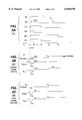
- FIG. 1 a block diagram of a CMOS imager system, in accordance with an embodiment of the present invention
- FIG. 2 is a circuit diagram illustrating an APS circuit of the APS array of the system of FIG. 1, and a linear CDS circuit and extended dynamic range (XDR) CDS circuit of the CDS rows the system of FIG. 1, in further detail;
- XDR extended dynamic range
- FIG. 3A is a timing diagram illustrating the signal waveforms used to operate the APS circuit and CDS circuits of FIG. 2 during a horizontal blanking period, in accordance with an embodiment of the present invention
- FIGS. 3B-C illustrate exemplary voltage signals of the APS circuit and CDS circuits of FIG. 2 produced during a bright scene utilizing XDR and a dark scene that does not utilize XDR, respectively;
- FIG. 4 is a graph illustrating the linear and XDR signal response of the system of FIG. 1;
- FIG. 5A is a timing diagram illustrating the signal waveforms used to operate the APS circuit and CDS circuits of FIG. 2 during a horizontal blanking period, in accordance with an alternative multi-breakpoint embodiment of the present invention.
- FIG. 5B is a graph illustrating the linear and XDR signal response of the system of FIG. 2, in accordance with the multi-breakpoint embodiment of FIG. 5A.
- an XDR imaging system reads out both XDR and linear channels from a pixel circuit so that the channels may be spliced together without being adversely affected by variations in breakpoint of the pixel circuit.
- the XDR imaging system is a CMOS-based imaging system having an array of APS pixel circuits, which employs at least two separate CDS circuits to provide separate channels for each of the two signal response ranges, linear and XDR.
- the linear and XDR channels may be spliced together to obtain a signal S that responds linearly to the light intensity over the entire dynamic range up to the saturation limit of the XDR channel, without being adversely affected by variations in breakpoint of the particular APS pixel circuit.
- Imager system 100 comprises processor 110, CMOS APS array 120 coupled to processor 110 by bus 115, and CDS rows 130, coupled by bus 125 to APS array 120.
- APS array 120 may be a 640(H) ⁇ 480(V) APS array of APS circuits.
- CDS rows 130 contains two separate rows or registers 131 and 132 of 640 CDS circuits each.
- CDS rows 130 contains two CDS circuits, one for the linear channel and one for the XDR channel, for each column of APS array 120.
- CDS rows 130 thus comprises a dual-register CDS means.
- each APS circuit provides an output voltage signal related to the intensity of light that has been applied to the APS circuit's photodetector region during the previous integration period (the period during which the photodetectors integrate charge).
- the output signal of each APS circuit of the activated row is sampled and held by the CDS circuit for the same column. Thereafter, the output of each of the 640 CDS circuits is consecutively applied to a buffer, so that the signal for each column may be amplified and, if desired, applied to an A/D converter (not shown) for further signal processing, and displayed on a monitor (not shown).
- CMOS imager utilizing a single CDS circuit to sample and hold the output signal for an APS pixel circuit is described in U.S. patent application Ser. No. 08/867,577, filed Jun. 2, 1997 (for "CMOS Imager with Reduced Fixed Pattern Noise,” attorney docket no. SAR 11994, inventor Sauer, Donald Jon), the entirety of which is incorporated herein by reference.
- another XDR imaging system employing either a CCD or CMOS imager, is described in U.S. patent application Ser. No. 08/867,652, filed Jun. 2, 1997 (for "Extended Dynamic Range Imaging System and Method," attorney docket no. SAR 12217, inventors McCaffrey, Nathaniel Joseph, et al.), the entirety of which is also incorporated herein by reference.
- a dual-register CDS means having two rows of CDS circuits and thus two CDS circuits per column, is used to read the separate linear and XDR channels of a given APS pixel after the integration period, so as to eliminate or reduce the effects of different pixel breakpoints, as described in further detail below.
- CMOS imager APS circuit or pixel 210 of APS array 120 comprises photodetector 216 and three NMOS field-effect transistors M1, M2, and M3.
- photodetector 216 is an N+ to p-substrate photodiode.
- APS circuit 210 is also coupled to bus lines supplying the following signals provided by processor 110: phase reset signal PR(x) and row select RS(x).
- phase reset signal PR(x) and row select RS(x) The parenthetical symbol (x) refers to the x-y coordinate system describing columns (the x coordinate) or rows (the y coordinate) of the APS pixel array, which allows selected columns and rows of the array to be specified for activation.
- Photodetector 216 is electrically coupled between ground and the source terminal of transistor M1 and the gate terminal of transistor M2.
- the gate terminal of transistor M1 is coupled to the PR signal line, and the drain terminal of transistor M1 is coupled to source voltage V DO (e.g., +5V), which is also coupled to the drain terminal of transistor M2.
- V DO source voltage
- the source terminal of transistor M2 is coupled to the drain terminal of transistor M3, the source terminal of which is coupled to DS circuits 230, 240 via the column read (Col -- Read(x)) line 220.
- the gate terminal of transistor M3 is coupled to the RS signal line.
- Transistors M2 and M3 are used to output onto line 220 a voltage VCR, which is a known multiple of voltage V DIODE , whenever the RS signal is high, during read out of the signal corresponding to the light signal charge accumulated.
- Transistor M2 is used as a source follower to drive column read line Col -- Read(x) in selected rows.
- Transistor M3 serves to isolate APS circuit 210 from line 220 when other rows of APS array 120 are being read.
- Reset transistor M1 (preferably an NMOS transistor) is used to reset V DIODE to a given level under control of input signal PR.
- a PR signal of 7V brings V DIODE up to approximately 5V, if it is lower than 5V.
- a PR signal of 3.5V brings V DIODE up to approximately 3.5V, if it is lower than 3.5V; however, if V DIODE is more than 3.5V, e.g. 4V, then a PR signal of 3.5V has no effect on V DIODE .
- V DIODE ⁇ 3.5V
- Vtn the NMOS conduction threshold of reset transistor M1.
- V DIODE Before the beginning of an integration period, or to reset V DIODE to the XDR clamp potential (e.g., 3.5V) at the beginning of the second portion of the integration period.
- XDR clamp potential e.g. 3.5V
- a similar resetting operation may be used during readout of the XDR channel, as described in further detail below.
- APS circuit 210 in one embodiment, is formed from 0.5 ⁇ m CMOS single-polysilicon, triple-metal (SPTM) process design rules and technology. This may be used, for example, to form a 640(H) ⁇ 480(V) APS array having a 4.8 ⁇ 3.6 mm image size, which is compatible with 1/3" optics; or a 640(H) ⁇ 480(V) APS array having a 3.6 ⁇ 2.7 mm image size, which is compatible with 1/4" optics.
- SPTM triple-metal
- photodetectors 216 may be utilized for photodetector 216 instead of a photodiode, such as virtual gate buried n-channel photodetector or a photogate detector.
- a virtual gate photodetector provides better blue response than do polysilicon photogates, fabrication of virtual gate detectors requires two additional implantation steps compared to the normal CMOS process, and therefore may not be feasible with some existing low-cost IC fabrication processes.
- Linear CDS circuit 230 contains transistor M8, coupled at its gate to V DO , transistor M4, coupled at its gate to sample and hold signal SH1, and capacitors C1 and C2, intercoupled as illustrated.
- Transistor M5 is coupled at its gate to clamp signal C1.
- Circuit 230 outputs the linear, or CDS LIN , signal.
- circuit 240 outputs the XDR signal CDS XDR Processor 110 provides the various phase reset, row select, clamp, and sample and hold signals applied to the components of APS pixel circuit 210 and CDS circuits 230, 240, through buses 115, 215.
- a current source (not shown) preferably is coupled in series with line 220, which provides a 20 ⁇ A load current.
- Each of capacitors C1, C2, C3, and C4 preferably has a capacitance of 1pF.
- capacitors C1 and C2, with accompanying transistors or switches M4 and M5, are used to implement the linear CDS function for each column, and to perform horizontal read out to a buffer.
- CDS circuit 230 The function of CDS circuit 230 is to capture and provide a CDS output voltage CDS LIN that indicates the change in APS output voltage V CR on line 220 corresponding to the linear channel. In order to do this, the change in APS output voltage V CR must be reflected in the CDS output voltage CDS LIN . As will be appreciated by those skilled in the art, this voltage change may be reflected by a voltage V LIN across capacitor C1 by first sampling and holding voltage V CR on line 220 before applying the APS output voltage thereto by switching on transistor M3. Then, transistor M3 is switched on by row select signal RS, which changes the voltage V CR on line 220. This change is thus reflected in the voltage stored on capacitor C2.
- the CDS LIN signal may be gated out, for example to a buffer (not shown) when desired by switching off transistor M4 to isolate capacitors C1 and C2 from APS circuit 210 and col -- read line 220, so that they form a series capacitance, and the APS output voltage is represented as a net signal charge stored in the series connection of capacitors C1 and C2. This may be read out in a known way to enable a processor to determine the signal change output by APS circuit 210.
- CDS circuit 240 may be operated to capture CDS XDR that indicates the change in APS output voltage V CR on line 220 corresponding to the XDR channel.
- the operation of CDS circuits 230, 240 are described in further detail below with reference to FIGS. 3A-C.
- FIG. 3A there is shown a timing diagram 310 illustrating the waveforms used to operate APS circuit 210 and CDS circuits 130 of FIG. 2 during a horizontal blanking period, in accordance with the present invention.
- FIGS. 3B and 3C illustrate exemplary voltage signals of APS circuit 210 and CDS circuits 130 of FIG. 2 produced during a bright scene utilizing XDR and a dark scene that does not utilize XDR, respectively.
- the input signals RS, PR, CL1, SH1, CL2, and SH2 are generated by signal generation circuitry, such as general-purpose programmed processor 110.
- photodetector 216 has been accumulating, or "integrating," charge in accordance with the light intensity reaching the surface area of photodetector 216, during the preceding integration period.
- the integration period begins after the row containing APS circuit 210 is reset after the previous read of the row, typically 1/30 or 1/60 second previously, depending upon the frame display rate. At this time, PR pulses to 7V, brining V DIODE up to an initial 5V level (the "initial diode reset level"), which gradually decreases during the integration period depending on the light impinging on photodiode 216.
- each APS circuit is reset once again by the signal on line PR being switched from 2V to 7V, which brings V DIODE up to 5.0V, so that during the next frame, light is once again accumulated during another integration period.
- a negative charge accumulates, thereby lowering the initial diode reset level of 5.0V in accordance with the intensity of the light integrated during this period.
- This voltage can reach a minimum of approximately 2.5V before saturation occurs (the "minimum diode level").
- a 1.5V signal variation of V DIODE between 5.0V and 3.5V is used for the linear range, and the remaining 1V signal variation between 3.5V and 2.5V can be used for XDR (and also for linear range for lower levels of light).
- V DIODE may be implemented by resetting V DIODE to an XDR reset voltage (e.g., 3.5V) a short time before the end of the integration period, thus dividing the integration period into first and second periods.
- V DIODE is reset to an XDR reset voltage of 3.5V.
- (1H is the period of the horizontal line rate, nominally 63.5 ⁇ s for NTSC standard video rates.)
- V DIODE can fall from 3.5V so as to allow some contrast to indicate the bright light that has saturated the linear range. If, however, V DIODE >3.5V, V DIODE will not be changed by the resetting operation at 450H.
- V DIODE will be in the range of 5.0V to 2.5V (i.e., between the initial diode reset level and the minimum diode level). If V DIODE is below the XDR clamp potential (3.5V), then the difference between V DIODE and 3.5V will represent the component accumulated after 450H, which will be an XDR component if there was saturation of the linear channel.
- XDR clamp potential 3.5V
- various techniques may be used to determine the total overall light that has impinged on photodetector 216 during the integration period. For example, the relative times of the XDR and linear portions may be designated as T XDR and T LIN , respectively.
- these times are 50H and 500H (i.e., 50H+450H), respectively.
- CDS XDR ⁇ (T XDR /(T LIN -T XDR ) ⁇ CDS LIN
- CDS XDR >(T XDR /(T LIN -T XDR ) ⁇ CDS LIN
- splicing must be performed, as described in further detail below, to obtain a signal S that responds linearly to the light intensity over the entire dynamic range up to the saturation limit of the XDR channel.
- time t -1 designates a time just after the end of the integration period and just before the beginning of the readout of the XDR and linear channels.
- V DIODE Prior to time t -1 , in both the bright scene case and dark scene case, V DIODE has decreased from an initial voltage of 5V to a lower voltage depending on how much light impinged on diode 216 during the integration period.
- V DIODE has fallen to 2.5V, well below the 3.5V reset voltage to which diode 216 was reset just 50H before the end of the 500H integration period.
- V DIODE has fallen only to 4.0V, which is above the 3.5V reset voltage level.
- the dual CDS circuits 230, 240 are controlled by control signals such that output signal S is produced, and is not affected by small variations in the XDR reset voltage.
- clamp signal CL2 (for XDR CDS circuit 240) switches low, thereby opening switch M7 and thus holding a reference voltage V C4 onto capacitor C4 equal to the initial APS output voltage V CR (i.e., 2.5V and 4.0V for the bright and dark scenes, respectively).
- PR then switches to 3.5V, to bring V DIODE up to the XDR clamp level (3.5V), if necessary.
- V CR and thus V LIN and V XDR , rise to 3.5V from 2.5V (FIG. 3B), a rise of 1V (which corresponds to the XDR component of the APS output signal).
- V C4 does not change, and thus stays at 2.5V, thus causing CDS XDR to increase by the difference, or 1.0V (3.5V-2.5V).
- V CR and thus V LIN and V XDR , do not change, since these voltages are already at 4.0V and thus cannot be "pulled up" to 3.5V.
- phase reset signal PR turns off, and, a short time later, at time t 2 both sample and hold signal SH2 and clamp signal CL1 turn off.
- Turning off SH2 thus holds onto V XDR the XDR signal, with the difference of 1.0V held as V C4
- Turning off CL1 opens switch M5 and thus holds a reference voltage V C2 onto capacitor C2 equal to the linear portion only of the signal, since V DIODE has already been pulled up to the XDR clamp level (3.5V), if necessary.
- V C2 and V LIN are 3.5V, the saturated linear level for the first 450H portion of the integration period; and 4V in the dark scene case.
- phase reset signal PR pulses to 7.0V, to bring V DIODE and thus V CR up to the initial level of 5.0V.
- V LIN thus rises from 3.5V to 5.0V; and in the dark scene, from 4.0V to 5.0V.
- V XDR does not change in either case since SH2 (and thus transistor M6) has already been turned off.
- M5 is open, when V LIN rises 5.0V, V C2 does not change.
- CDS LIN increases by the difference between 5.0V and the previous VLN (i.e., 3.5V or 4.0V in the bright and dark scenes, respectively).
- FIG. 4 there is depicted a graph 400 illustrating the linear and XDR signal response of the system 100 of FIG. 1.
- the linear channel will not be saturated. However, for light beyond this point, the linear channel is saturated, and V DIODE will have fallen below 3.5V and thus will be reset to the XDR clamp potential at 450H.
- the XDR of the system is employed, in which case a breakpoint occurs in the signal response at approximately 11 lux. The breakpoint does not occur exactly at 10 lux, as will be appreciated, since V DIODE may be just at 3.5V exactly at 450H and thus not quite saturated, in which case additional light falling at a similar intensity in the remaining 50H portion of the integration period adds to the linear signal.
- the XDR channel has one-tenth the slope of the linear channel.
- the linear and XDR channels may be digitally spliced together to obtain a signal which responds linearly to the light intensity over the entire dynamic range up to the XDR channel saturate limit (e.g., 100 lux in this case).
- the following algorithm may be employed for this splicing operation:
- S is the spliced signal combining the linear and XDR channels.
- the XDR channel is sampled by the XDR CDS circuit 240, and the linear channel is sampled by the linear CDS circuit 230.
- XDR CDS circuit 240 samples the entire signal change, clamps this value, and then resets the pixel to drain off the XDR amount, and then samples this new value.
- XDR CDS circuit 240 thus samples and stores the change in the XDR component, which is reflected in CDS XDR (at time t 0 ). However, the change is with respect to the actual XDR clamp potential of the pixel (APS circuit 210), even if this is different from the ideal of 3.5V.
- This difference signal accurately corresponds to the actual change in V DIODE caused by photons striking after diode 216 was reset to the clamp potential at 450H, because at this time diode 216 was reset to the actual, not ideal, XDR clamp potential as well.
- the XDR signal sampled and held by XDR CDS circuit 240 is an accurate reflection of the XDR signal even though the XDR clamp potential is different from the ideal. This is thus more accurate than if only a single CDS circuit were used, when the difference information would be lost.
- the actual XDR clamp potential is itself stored in linear CDS circuit 230 as a reference, and the pixel is then reset completely to the initial diode reset level (ideally, to 5V).
- the XDR clamp potential ideally 3.5V
- the initial diode reset level will also be off by a similar amount, so that the difference between the actual initial diode reset level and the actual XDR clamp potential will be closer to the same difference for neighboring pixels, even if the XDR clamp potentials vary from one another.
- information about where the breakpoint is, is lost, and thus variations between pixels are greater.
- the present invention can eliminate or reduce breakpoint differences, as will be appreciated.
- the present invention therefore, advantageously allows the extended dynamic range combined signal response to be provided while reducing the adverse effects caused by inter-pixel breakpoint-related differences, such as differences in the XDR clamp potential, as will be appreciated by those skilled in the art.
- a manufacturing difference for APS circuit 210 causes the XDR clamp potential to be 3.4V instead of the ideal of 3.5V.
- the output signals will be illustrated here for both the ideal XDR clamp potential (3.5V) case and the assumed actual XDR clamp potential (3.4V) case, using the bright scene case of FIG. 3B as an example.
- XDR CDS circuit 240 uses the actual XDR clamp potential 3.4V to capture the XDR signal, it still captures the delta 1.0V, the same as captured in the ideal, 3.5V case.
- the difference between the actual initial diode reset level and the actual XDR clamp level is captured.
- the actual initial diode reset level may be 4.9V in this case, instead of the ideal 5.0V, for the same or similar reasons that the actual XDR clamp potential is 3.4V instead of 3.5V.
- the signal from the first portion is captured, which is the same as that which would be captured in the ideal case.
- More accurate capture of the linear signal also helps reduce the above-described artifacts. Nevertheless, even in cases where the linear signal still contains some error due to breakpoint differences, the present invention reduces the major portion of the fact and error due to the XDR signal, as described above.
- a single-breakpoint, dual-slope XDR system is employed, having two separate CDS circuits, one for each slope of the signal response characteristic.
- a multi-breakpoint system may be employed to help reduce artifacts generated when only two slopes (and one breakpoint) are employed. Such artifacts may arise due to sharp peaks in the derivative of the imager response at the breakpoint, especially if there is a large difference between the linear and XDR channel gain. Even if it is possibly to seamlessly reconstruct (splice) the separated linear and XDR channel components, the additional gain of the XDR channel may be high enough so that the random noise of that channel is visible above the shot noise of the signal in the linear channel.
- a relatively smooth non-linear compression characteristic which approximates a logarithmic (or other) response may be provided by using a piece-wise linear response with multiple breakpoints.
- N breakpoints are employed, having N+1 segments, or slopes, i.e. the first, linear segment, and N additional XDR segments.
- the associated signals for each segment may be read out in any number of channels, from 1 to N+1.
- the choice of the number of signal channels allows a tradeoff between system complexity and pixel-to-pixel matching of the individual breakpoints.
- two channels may be employed, as in system 100 described above, even for a multiple-breakpoint system; or more than two, up to N+1, channels and thus CDS circuits may be employed.
- the last CDS circuit is used to reconstruct N+2-C>1 segments, thereby reducing the ability to compensate for inter-pixel differences in the breakpoints between these segments.
- the last CDS circuit is used to reconstruct N+2-C>1 segments, thereby reducing the ability to compensate for inter-pixel differences in the breakpoints between these segments.
- the first-the change in slope between adjoining segments becomes relatively small, thus reducing the artifacts produced by inter-pixel breakpoint mismatches.
- only two CDS circuits may be employed, one for the linear response and the other for the XDR response of all other slopes.
- the method employed in reading out the signal into two channels for a single breakpoint suppresses the first order Vt variations in the pixel reset transistor M1.
- a single channel readout which contains the entire N+1 segment piece wise linear response may be used, along with time multiplexing.
- the method of reading out a CMOS APS imager to obtain an N+1 -segment piece wise linear signal response is described in further detail as follows.
- the N+1-segment piece wise linear signal response can be separated into any number of signal channels, from 1 to N+1, as described above, and the associated readout method may be logically divided into two parts.
- the non-linear response is controlled as described in Levine, for CMOS type imager systems.
- the integration time of the separate segments in the response is achieved by addressing a row in the imager M(x) line times before it is read out (i.e. before the end to the integration period) and momentarily raising the row reset line (e.g., PR in FIG. 2) to a value of VM(x), where M(x+1) >M(x) and VM(x+1) >VM(x); where M(x) is an integer value which may vary from 1 to the total number of lines in a frame.
- This operation may be conveniently and is preferably performed during the horizontal blanking period of a line time, in a system having an architecture which provides for random addressing of rows.
- Approximately 1 ⁇ s may be required to latch a new row address and pulse the row select and momentarily raise the row reset line in the selected row to VM(x). Therefore, at a system having a 30 frame per second (fps) readout rate using a horizontal blanking period of 10 ⁇ s, it is possible to have about five breakpoints and still allow 5 ⁇ s for the dual-CDS readout operations described above.
- fps frame per second
- the integrated charge stored in the pixel is read out into a number of channels ranging from 1 to N+1, by using a CDS circuit for each signal channel, which clamps to the value of the pixel after the row reset line is pulsed to a value of VM(x) and then samples the value of the pixel after the row reset line is pulsed to a value of VM(x+1).
- the multiple sets of CDS circuits in each column are thus loaded with respective signals during the horizontal blanking period, and may be read out in parallel during the active line time, as described in further detail below with reference to FIGS. 5A-B.
- FIG. 5A there is shown a timing diagram 510 illustrating the signal waveforms used to operate APS circuit 210 and CDS circuits 130 of FIG. 2 during the horizontal blanking period, in accordance with an alternative multi-breakpoint embodiment of the present invention.
- FIG. 5B is a graph 550 illustrating the linear and XDR signal response of system 100 of FIG. 1, in accordance with the multi-breakpoint embodiment of FIG. 5A.
- the input signals Vadd, Vstrb, Grh, CL1, SH1, CL2, SH2, Grm, and Vrh are generated by signal generation circuitry, such as general-purpose programmed processor 110.
- the XDR signal is sampled, when SH2 switches low.
- signals Vadd is the Vertical Shift Register row address
- signal Vstrb is the Vadd latch pulse and will enable RS of the selected row
- signal Grh pulses the reset gate signal PR with a voltage equal to Vrh (7V)
- signal Grm pulses the reset gate signal PR with a voltage equal to Vrm (3.5V nominal)
- signal Vrh is an analog signal that turns the transistor on fully and charge the diode up to 5V (cleared). Vrm will turn the transistor on and charge the diode up to Vrm-Vth (XDR clear, or clamp level) leaving the linear signal alone.
- the signals m, m+32, m+16, et seq. are row addresses. By addressing 32 lines ahead of the current read out line m, the signal can be cleared for a reduced integration time of 32 lines. Either the XDR or linear signal can be cleared. By clearing the linear signal, the XDR signal is by default cleared, so that linear clearing has to be performed with an offset line address greater than the XDR clear line offset address. For instance, the linear signal can be cleared 32 lines ahead and the XDR 16 lines ahead, but not the opposite. In addition, in this embodiment, the pixel may be cleared without running the signal through the CDS circuit.
- graph 550 shows the signal response for a 4-breakpoint, 5-segment system, having breakpoints BP1, BP2, BP3, and BP4.
- BP1 corresponds to the first 525H of a 585H system
- BP2 occurs 32H later, and so for
- a more smooth, logarithmic-approximating signal response is provided by using multiple breakpoints.
- FIGS. 5A-B only two CDS circuits are employed, one for the linear response and the other for the XDR response of all other slopes (i.e., for those segments past BP1).
- the dual-register CDS means of CDS rows 130 of FIGS. 1 and 2 may be employed for signal readout.
- multiple segments are employed but only a single channel and CDS circuit is employed per column, and time multiplexing is used to readout the different signal response segments.
- This embodiment requires more complexity and a higher horizontal readout clock rate for the same operating frame rate of the imager.
- the algorithm presented above for providing spliced signal S may be modified to minimize dark noise.
- the XDR channel may be "muted" when the linear signal CDS LIN is below a relatively high fixed threshold, e.g. 80% of the saturation level, when the shot noise of the linear signal is substantially higher than the dark noise of the XDR channel.
Abstract
Description
______________________________________
If CDS.sub.XDR  ≦ (T.sub.XDR /(T.sub.LIN  - T.sub.XDR) ·
CDS.sub.LIN           {i.e., if there was no
                      saturation of the linear
                      channel; i.e. I ≦
                      11 lux}
then S = CDS.sub.LIN  + CDS.sub.XDR ;
                      {combine the signal
                      accumulated in both
                      portions of the
                      integraton period}
If CDS.sub.XDR  > (T.sub.XDR /(T.sub.LIN  - T.sub.XDR) ·
CDS.sub.LIN           {if there was
                      saturation of the
                      linear channel}
then S = CDS.sub.LIN  + CDS.sub.XDR  +
                      {combine the signal
                      accumulated in both
(T.sub.LIN /T.sub.XDR)[CDS.sub.XDR  -
                      portions of the
                      integration period}
(T.sub.XDR /(T.sub.LIN  - T.sub.XDR)) · CDS.sub.LIN ]
______________________________________
Claims (9)
Priority Applications (8)
| Application Number | Priority Date | Filing Date | Title |
|---|---|---|---|
| US09/087,087 US6040570A (en) | 1998-05-29 | 1998-05-29 | Extended dynamic range image sensor system |
| EP99927117A EP1082849B1 (en) | 1998-05-29 | 1999-05-28 | Extended dynamic range image sensor system |
| PCT/US1999/012045 WO1999062244A1 (en) | 1998-05-29 | 1999-05-28 | Extended dynamic range image sensor system |
| DE69920687T DE69920687T2 (en) | 1998-05-29 | 1999-05-28 | IMAGE SENSOR WITH EXTENDED DYNAMIC RANGE |
| JP2000551532A JP2002517135A (en) | 1998-05-29 | 1999-05-28 | Extended dynamic range image sensor system |
| KR1020007013393A KR100552946B1 (en) | 1998-05-29 | 1999-05-28 | Extended dynamic range image sensor system |
| AU44099/99A AU4409999A (en) | 1998-05-29 | 1999-05-28 | Extended dynamic range image sensor system |
| US09/497,898 US6441852B1 (en) | 1998-05-29 | 2000-02-04 | Extended dynamic range image sensor system |
Applications Claiming Priority (1)
| Application Number | Priority Date | Filing Date | Title |
|---|---|---|---|
| US09/087,087 US6040570A (en) | 1998-05-29 | 1998-05-29 | Extended dynamic range image sensor system |
Related Child Applications (1)
| Application Number | Title | Priority Date | Filing Date |
|---|---|---|---|
| US09/497,898 Division US6441852B1 (en) | 1998-05-29 | 2000-02-04 | Extended dynamic range image sensor system |
Publications (1)
| Publication Number | Publication Date |
|---|---|
| US6040570A true US6040570A (en) | 2000-03-21 |
Family
ID=22203041
Family Applications (2)
| Application Number | Title | Priority Date | Filing Date |
|---|---|---|---|
| US09/087,087 Expired - Lifetime US6040570A (en) | 1998-05-29 | 1998-05-29 | Extended dynamic range image sensor system |
| US09/497,898 Expired - Lifetime US6441852B1 (en) | 1998-05-29 | 2000-02-04 | Extended dynamic range image sensor system |
Family Applications After (1)
| Application Number | Title | Priority Date | Filing Date |
|---|---|---|---|
| US09/497,898 Expired - Lifetime US6441852B1 (en) | 1998-05-29 | 2000-02-04 | Extended dynamic range image sensor system |
Country Status (7)
| Country | Link |
|---|---|
| US (2) | US6040570A (en) |
| EP (1) | EP1082849B1 (en) |
| JP (1) | JP2002517135A (en) |
| KR (1) | KR100552946B1 (en) |
| AU (1) | AU4409999A (en) |
| DE (1) | DE69920687T2 (en) |
| WO (1) | WO1999062244A1 (en) |
Cited By (42)
| Publication number | Priority date | Publication date | Assignee | Title |
|---|---|---|---|---|
| US6180935B1 (en) * | 1999-01-25 | 2001-01-30 | Lockheed Martin Corporation | Dynamic range extension of CCD imagers |
| US6188433B1 (en) * | 1999-02-02 | 2001-02-13 | Ball Aerospace & Technologies Corp. | Method and apparatus for enhancing the dynamic range of a CCD sensor |
| US20020012057A1 (en) * | 2000-05-26 | 2002-01-31 | Hajime Kimura | MOS sensor and drive method thereof |
| US6348681B1 (en) | 2000-06-05 | 2002-02-19 | National Semiconductor Corporation | Method and circuit for setting breakpoints for active pixel sensor cell to achieve piecewise linear transfer function |
| US6365950B1 (en) * | 1998-06-02 | 2002-04-02 | Samsung Electronics Co., Ltd. | CMOS active pixel sensor |
| US20020067415A1 (en) * | 2000-06-28 | 2002-06-06 | Stmicroelectronics Ltd | Image sensors with multiple integration/read cycles |
| WO2002056584A1 (en) * | 2001-01-11 | 2002-07-18 | Smal Camera Technologies | Adaptive sensitivity control, on a pixel-by-pixel basis, for a digital imager |
| US20020118289A1 (en) * | 2000-12-14 | 2002-08-29 | Soo-Chang Choi | CMOS image sensor having a chopper-type comparator to perform analog correlated double sampling |
| US20020154243A1 (en) * | 2000-12-19 | 2002-10-24 | Fife Keith Glen | Compact digital camera system |
| US20020159101A1 (en) * | 2001-04-25 | 2002-10-31 | Timothy Alderson | Scene-based non-uniformity correction for detector arrays |
| US20020159648A1 (en) * | 2001-04-25 | 2002-10-31 | Timothy Alderson | Dynamic range compression |
| US6486460B1 (en) * | 1998-09-11 | 2002-11-26 | Nec Corporation | Solid-state image sensing device and method of driving the same |
| US6512544B1 (en) * | 1998-06-17 | 2003-01-28 | Foveon, Inc. | Storage pixel sensor and array with compression |
| US20030038887A1 (en) * | 2001-08-24 | 2003-02-27 | Mccaffrey Nathaniel Joseph | Fully integrated solid state imager and camera circuitry |
| US6567124B1 (en) * | 1999-12-01 | 2003-05-20 | Ball Aerospace & Technologies Corp. | Electronic image processing technique for achieving enhanced image detail |
| US6600471B2 (en) | 2000-07-28 | 2003-07-29 | Smal Camera Technologies, Inc. | Precise MOS imager transfer function control for expanded dynamic range imaging |
| US20030206236A1 (en) * | 2002-05-06 | 2003-11-06 | Agfa Corporation | CMOS digital image sensor system and method |
| US20040021057A1 (en) * | 2002-07-30 | 2004-02-05 | Drowley Clifford I. | Pixel sensor circuit device and method thereof |
| US20040041927A1 (en) * | 2002-08-29 | 2004-03-04 | Kwang-Bo Cho | High intrascene dynamic range NTSC and PAL imager |
| US20040155973A1 (en) * | 2003-01-13 | 2004-08-12 | Chang-Min Bea | Image sensor having clamp circuit |
| US6777662B2 (en) | 2002-07-30 | 2004-08-17 | Freescale Semiconductor, Inc. | System, circuit and method providing a dynamic range pixel cell with blooming protection |
| US20040174754A1 (en) * | 2003-01-08 | 2004-09-09 | Hae-Seung Lee | Precise CMOS imager transfer function control for expanded dynamic range imaging using variable-height multiple reset pulses |
| US20040182990A1 (en) * | 2001-11-06 | 2004-09-23 | Dai Tie Jun | Zero DC current readout circuit for CMOS image sensor using a precharge capacitor |
| US20050030401A1 (en) * | 2003-08-05 | 2005-02-10 | Ilia Ovsiannikov | Method and circuit for determining the response curve knee point in active pixel image sensors with extended dynamic range |
| US20050083421A1 (en) * | 2003-10-16 | 2005-04-21 | Vladimir Berezin | Dynamic range enlargement in CMOS image sensors |
| US20050146617A1 (en) * | 2003-12-25 | 2005-07-07 | Canon Kabushiki Kaisha | Imaging apparatus for processing noise signal and photoelectric conversion signal |
| US6921897B1 (en) | 2000-09-21 | 2005-07-26 | Lockheed Martin Corporation | Circuit and method for varying the integration time of moving charges from a photodetector |
| US20050212936A1 (en) * | 2004-03-25 | 2005-09-29 | Eastman Kodak Company | Extended dynamic range image sensor with fixed pattern noise reduction |
| US6975355B1 (en) | 2000-02-22 | 2005-12-13 | Pixim, Inc. | Multiple sampling via a time-indexed method to achieve wide dynamic ranges |
| US20060017830A1 (en) * | 2004-07-23 | 2006-01-26 | Chih-Cheng Hsieh | Active pixel sensor with isolated photo-sensing region and peripheral circuit region |
| US20060071254A1 (en) * | 2004-09-28 | 2006-04-06 | Rhodes Howard E | High dynamic range image sensor |
| US20060082670A1 (en) * | 2004-10-14 | 2006-04-20 | Eastman Kodak Company | Interline CCD for still and video photography with extended dynamic range |
| US7057147B1 (en) | 2003-12-17 | 2006-06-06 | Itt Manufacturing Enterprises Inc. | Imaging system and method for collecting energy from at least two sensing elements adjacent one another between rows of sensing elements |
| US20060188169A1 (en) * | 2001-04-25 | 2006-08-24 | Lockheed Martin Corporation | Extended range image processing for electro-optical systems |
| US7173666B1 (en) | 2002-08-22 | 2007-02-06 | Smal Camera Technologies | System and method for displaying a non-standard aspect ratio image on a standard aspect ratio monitor |
| CN1309088C (en) * | 2000-06-23 | 2007-04-04 | 皮克斯尔普拉斯有限公司 | Complementary metallic oxide semiconductor imaging sensor and its driving method |
| US20070235631A1 (en) * | 2006-03-30 | 2007-10-11 | Micron Technology, Inc. | Reducing noise in an imager |
| US20080212895A1 (en) * | 2007-01-09 | 2008-09-04 | Lockheed Martin Corporation | Image data processing techniques for highly undersampled images |
| US20090086072A1 (en) * | 2007-10-02 | 2009-04-02 | Electronics And Telecommunications Research Institute | DUAL CDS/PxGA CIRCUIT |
| US20090109313A1 (en) * | 2007-10-30 | 2009-04-30 | Xinqiao Liu | Self-Triggering CMOS Image Sensor |
| US20100271517A1 (en) * | 2009-04-24 | 2010-10-28 | Yannick De Wit | In-pixel correlated double sampling pixel |
| CN1838741B (en) * | 2005-03-09 | 2011-08-31 | 三星电子株式会社 | Solid state image sensing device and method for subsampling using inter-column analog domain signal summation |
Families Citing this family (19)
| Publication number | Priority date | Publication date | Assignee | Title |
|---|---|---|---|---|
| KR100265364B1 (en) * | 1998-06-27 | 2000-09-15 | 김영환 | Cmos image sensor with wide dynamic range |
| JP3725007B2 (en) * | 2000-06-06 | 2005-12-07 | シャープ株式会社 | Logarithmic conversion type pixel structure and solid-state imaging device using the same |
| CA2350416A1 (en) * | 2000-12-20 | 2002-06-20 | Symagery Microsystems Inc. | Image sensor with correlated double sampling technique using switched-capacitor technology |
| EP1594321A3 (en) * | 2004-05-07 | 2006-01-25 | Dialog Semiconductor GmbH | Extended dynamic range in color imagers |
| EP1608183A1 (en) * | 2004-06-14 | 2005-12-21 | Dialog Semiconductor GmbH | Matrix circuit for imaging sensors |
| EP1679907A1 (en) * | 2005-01-05 | 2006-07-12 | Dialog Semiconductor GmbH | Hexagonal color pixel structure with white pixels |
| CN100433197C (en) * | 2005-03-17 | 2008-11-12 | 北京思比科微电子技术有限公司 | Low noisc relative double-sampling circuit |
| US8139130B2 (en) | 2005-07-28 | 2012-03-20 | Omnivision Technologies, Inc. | Image sensor with improved light sensitivity |
| US8274715B2 (en) | 2005-07-28 | 2012-09-25 | Omnivision Technologies, Inc. | Processing color and panchromatic pixels |
| US7598998B2 (en) * | 2005-09-30 | 2009-10-06 | Honeywell International Inc. | Method and system for increasing the effective dynamic range of a random-access pixel sensor array |
| US7750960B2 (en) * | 2006-03-15 | 2010-07-06 | Honeywell International Inc. | System and apparatus for high dynamic range sensor |
| US7916362B2 (en) * | 2006-05-22 | 2011-03-29 | Eastman Kodak Company | Image sensor with improved light sensitivity |
| US8031258B2 (en) | 2006-10-04 | 2011-10-04 | Omnivision Technologies, Inc. | Providing multiple video signals from single sensor |
| WO2008120292A1 (en) * | 2007-02-28 | 2008-10-09 | Hamamatsu Photonics K.K. | Solid-state imaging apparatus |
| US7674648B2 (en) * | 2007-03-21 | 2010-03-09 | Eastman Kodak Company | Extended dynamic range using variable sensitivity pixels |
| DE102009028352A1 (en) * | 2009-08-07 | 2011-02-10 | Pmdtechnologies Gmbh | Photonic mixer device pixel array for producing color image on display, has linearization circuit connected to outlet of non-linear transistor by selection transistors to compensate non-linearity between charging quantity and output signal |
| JP6132283B2 (en) * | 2013-05-17 | 2017-05-24 | Nltテクノロジー株式会社 | Amplifier circuit and image sensor using the amplifier circuit |
| WO2016078713A1 (en) * | 2014-11-20 | 2016-05-26 | Teledyne Dalsa B.V. | A circuit controller for controlling a pixel circuit and a method of controlling a pixel circuit |
| US9986213B2 (en) | 2016-06-29 | 2018-05-29 | Omnivision Technologies, Inc. | Image sensor with big and small pixels and method of manufacture |
Citations (2)
| Publication number | Priority date | Publication date | Assignee | Title |
|---|---|---|---|---|
| US5600696A (en) * | 1995-10-11 | 1997-02-04 | David Sarnoff Research Center, Inc. | Dual-gain floating diffusion output amplifier |
| US5920345A (en) * | 1997-06-02 | 1999-07-06 | Sarnoff Corporation | CMOS image sensor with improved fill factor |
Family Cites Families (6)
| Publication number | Priority date | Publication date | Assignee | Title |
|---|---|---|---|---|
| US4819070A (en) * | 1987-04-10 | 1989-04-04 | Texas Instruments Incorporated | Image sensor array |
| JP3257802B2 (en) * | 1991-05-30 | 2002-02-18 | ソニー株式会社 | Solid-state imaging device and method of driving solid-state imaging device |
| US5276520A (en) * | 1991-06-07 | 1994-01-04 | Eastman Kodak Company | Enhancing exposure latitude of image sensors |
| JP3013584B2 (en) * | 1992-02-14 | 2000-02-28 | ソニー株式会社 | Solid-state imaging device |
| US5461425A (en) * | 1994-02-15 | 1995-10-24 | Stanford University | CMOS image sensor with pixel level A/D conversion |
| JP3915161B2 (en) * | 1997-03-04 | 2007-05-16 | ソニー株式会社 | Method for expanding dynamic range of solid-state image sensor with blooming prevention structure and solid-state image sensor |
-
1998
- 1998-05-29 US US09/087,087 patent/US6040570A/en not_active Expired - Lifetime
-
1999
- 1999-05-28 WO PCT/US1999/012045 patent/WO1999062244A1/en active IP Right Grant
- 1999-05-28 DE DE69920687T patent/DE69920687T2/en not_active Expired - Lifetime
- 1999-05-28 AU AU44099/99A patent/AU4409999A/en not_active Abandoned
- 1999-05-28 JP JP2000551532A patent/JP2002517135A/en active Pending
- 1999-05-28 KR KR1020007013393A patent/KR100552946B1/en not_active IP Right Cessation
- 1999-05-28 EP EP99927117A patent/EP1082849B1/en not_active Expired - Lifetime
-
2000
- 2000-02-04 US US09/497,898 patent/US6441852B1/en not_active Expired - Lifetime
Patent Citations (2)
| Publication number | Priority date | Publication date | Assignee | Title |
|---|---|---|---|---|
| US5600696A (en) * | 1995-10-11 | 1997-02-04 | David Sarnoff Research Center, Inc. | Dual-gain floating diffusion output amplifier |
| US5920345A (en) * | 1997-06-02 | 1999-07-06 | Sarnoff Corporation | CMOS image sensor with improved fill factor |
Cited By (76)
| Publication number | Priority date | Publication date | Assignee | Title |
|---|---|---|---|---|
| US6365950B1 (en) * | 1998-06-02 | 2002-04-02 | Samsung Electronics Co., Ltd. | CMOS active pixel sensor |
| US6512544B1 (en) * | 1998-06-17 | 2003-01-28 | Foveon, Inc. | Storage pixel sensor and array with compression |
| US6486460B1 (en) * | 1998-09-11 | 2002-11-26 | Nec Corporation | Solid-state image sensing device and method of driving the same |
| US6180935B1 (en) * | 1999-01-25 | 2001-01-30 | Lockheed Martin Corporation | Dynamic range extension of CCD imagers |
| US6188433B1 (en) * | 1999-02-02 | 2001-02-13 | Ball Aerospace & Technologies Corp. | Method and apparatus for enhancing the dynamic range of a CCD sensor |
| US6567124B1 (en) * | 1999-12-01 | 2003-05-20 | Ball Aerospace & Technologies Corp. | Electronic image processing technique for achieving enhanced image detail |
| US6975355B1 (en) | 2000-02-22 | 2005-12-13 | Pixim, Inc. | Multiple sampling via a time-indexed method to achieve wide dynamic ranges |
| US7224391B2 (en) * | 2000-05-26 | 2007-05-29 | Semiconductor Energy Laboratory Co., Ltd. | MOS sensor and drive method thereof |
| US8164652B2 (en) | 2000-05-26 | 2012-04-24 | Semiconductor Energy Laboratory Co., Ltd. | MOS sensor and drive method thereof |
| US20020012057A1 (en) * | 2000-05-26 | 2002-01-31 | Hajime Kimura | MOS sensor and drive method thereof |
| US7787039B2 (en) | 2000-05-26 | 2010-08-31 | Semiconductor Energy Laboratory Co., Ltd. | MOS sensor and drive method thereof |
| US6348681B1 (en) | 2000-06-05 | 2002-02-19 | National Semiconductor Corporation | Method and circuit for setting breakpoints for active pixel sensor cell to achieve piecewise linear transfer function |
| CN1309088C (en) * | 2000-06-23 | 2007-04-04 | 皮克斯尔普拉斯有限公司 | Complementary metallic oxide semiconductor imaging sensor and its driving method |
| US20020067415A1 (en) * | 2000-06-28 | 2002-06-06 | Stmicroelectronics Ltd | Image sensors with multiple integration/read cycles |
| US6600471B2 (en) | 2000-07-28 | 2003-07-29 | Smal Camera Technologies, Inc. | Precise MOS imager transfer function control for expanded dynamic range imaging |
| US6921897B1 (en) | 2000-09-21 | 2005-07-26 | Lockheed Martin Corporation | Circuit and method for varying the integration time of moving charges from a photodetector |
| USRE41865E1 (en) | 2000-12-14 | 2010-10-26 | Soo-Chang Choi | CMOS image sensor having a chopper-type comparator to perform analog correlated double sampling |
| US20020118289A1 (en) * | 2000-12-14 | 2002-08-29 | Soo-Chang Choi | CMOS image sensor having a chopper-type comparator to perform analog correlated double sampling |
| US6727486B2 (en) | 2000-12-14 | 2004-04-27 | Hynix Semiconductor Inc | CMOS image sensor having a chopper-type comparator to perform analog correlated double sampling |
| US20020154243A1 (en) * | 2000-12-19 | 2002-10-24 | Fife Keith Glen | Compact digital camera system |
| WO2002056584A1 (en) * | 2001-01-11 | 2002-07-18 | Smal Camera Technologies | Adaptive sensitivity control, on a pixel-by-pixel basis, for a digital imager |
| US20020105581A1 (en) * | 2001-01-11 | 2002-08-08 | Ichiro Masaki | Adaptive sensitivity control, on a pixel-by-pixel basis, for a digital imager |
| US8009206B2 (en) | 2001-01-11 | 2011-08-30 | Melexis Tessenderlo Nv | Adaptive sensitivity control, on a pixel-by-pixel basis, for a digital imager |
| US7760965B2 (en) | 2001-04-25 | 2010-07-20 | Lockheed Martin Corporation | Extended range image processing for electro-optical systems |
| US20020159648A1 (en) * | 2001-04-25 | 2002-10-31 | Timothy Alderson | Dynamic range compression |
| US20020159101A1 (en) * | 2001-04-25 | 2002-10-31 | Timothy Alderson | Scene-based non-uniformity correction for detector arrays |
| US6973218B2 (en) | 2001-04-25 | 2005-12-06 | Lockheed Martin Corporation | Dynamic range compression |
| US20060188169A1 (en) * | 2001-04-25 | 2006-08-24 | Lockheed Martin Corporation | Extended range image processing for electro-optical systems |
| US7103235B2 (en) | 2001-04-25 | 2006-09-05 | Lockheed Martin Corporation | Extended range image processing for electro-optical systems |
| US6901173B2 (en) | 2001-04-25 | 2005-05-31 | Lockheed Martin Corporation | Scene-based non-uniformity correction for detector arrays |
| CN100389596C (en) * | 2001-08-24 | 2008-05-21 | 迪亚洛格半导体有限公司 | Fully integrated solid state imager and camera circuitry |
| WO2003019829A2 (en) * | 2001-08-24 | 2003-03-06 | Dialog Semiconductor Gmbh | Fully integrated solid state imager and camera circuitry |
| US20030038887A1 (en) * | 2001-08-24 | 2003-02-27 | Mccaffrey Nathaniel Joseph | Fully integrated solid state imager and camera circuitry |
| US6992713B2 (en) * | 2001-08-24 | 2006-01-31 | Dialog Semiconductor Gmbh | Fully integrated solid state imager and camera display |
| WO2003019829A3 (en) * | 2001-08-24 | 2005-01-27 | Dialog Semiconductor Gmbh | Fully integrated solid state imager and camera circuitry |
| US6864476B2 (en) * | 2001-11-06 | 2005-03-08 | Omnivision Technologies, Inc. | Zero DC current readout circuit for CMOS image sensor using a discharge capacitor |
| US20040182990A1 (en) * | 2001-11-06 | 2004-09-23 | Dai Tie Jun | Zero DC current readout circuit for CMOS image sensor using a precharge capacitor |
| US20030206236A1 (en) * | 2002-05-06 | 2003-11-06 | Agfa Corporation | CMOS digital image sensor system and method |
| US20040021057A1 (en) * | 2002-07-30 | 2004-02-05 | Drowley Clifford I. | Pixel sensor circuit device and method thereof |
| US6777662B2 (en) | 2002-07-30 | 2004-08-17 | Freescale Semiconductor, Inc. | System, circuit and method providing a dynamic range pixel cell with blooming protection |
| US6906302B2 (en) | 2002-07-30 | 2005-06-14 | Freescale Semiconductor, Inc. | Photodetector circuit device and method thereof |
| US7173666B1 (en) | 2002-08-22 | 2007-02-06 | Smal Camera Technologies | System and method for displaying a non-standard aspect ratio image on a standard aspect ratio monitor |
| US7973842B2 (en) | 2002-08-29 | 2011-07-05 | Aptina Imaging Corporation | High intrascene dynamic range NTSC and PAL imager |
| US20040041927A1 (en) * | 2002-08-29 | 2004-03-04 | Kwang-Bo Cho | High intrascene dynamic range NTSC and PAL imager |
| US20080218621A1 (en) * | 2002-08-29 | 2008-09-11 | Micron Technology, Inc. | High intrascene dynamic range NTSC and PAL imager |
| US7382407B2 (en) | 2002-08-29 | 2008-06-03 | Micron Technology, Inc. | High intrascene dynamic range NTSC and PAL imager |
| US20040174754A1 (en) * | 2003-01-08 | 2004-09-09 | Hae-Seung Lee | Precise CMOS imager transfer function control for expanded dynamic range imaging using variable-height multiple reset pulses |
| US7417678B2 (en) * | 2003-01-08 | 2008-08-26 | Sensata Technologies, Inc. | Precise CMOS imager transfer function control for expanded dynamic range imaging using variable-height multiple reset pulses |
| US20040155973A1 (en) * | 2003-01-13 | 2004-08-12 | Chang-Min Bea | Image sensor having clamp circuit |
| US7394491B2 (en) | 2003-01-13 | 2008-07-01 | Magnachip Semiconductor, Ltd. | Image sensor having clamp circuit |
| US20070195183A1 (en) * | 2003-08-05 | 2007-08-23 | Ilia Ovsiannikov | Method and circuit for determining the response curve knee point in active pixel image sensors with extended dynamic range |
| US20050030401A1 (en) * | 2003-08-05 | 2005-02-10 | Ilia Ovsiannikov | Method and circuit for determining the response curve knee point in active pixel image sensors with extended dynamic range |
| US7768563B2 (en) | 2003-08-05 | 2010-08-03 | Aptina Imaging Corp. | Method and circuit for determining the response curve knee point in active pixel image sensors with extended dynamic range |
| US7456884B2 (en) | 2003-08-05 | 2008-11-25 | Aptina Imaging Corporation | Method and circuit for determining the response curve knee point in active pixel image sensors with extended dynamic range |
| US20050083421A1 (en) * | 2003-10-16 | 2005-04-21 | Vladimir Berezin | Dynamic range enlargement in CMOS image sensors |
| US7057147B1 (en) | 2003-12-17 | 2006-06-06 | Itt Manufacturing Enterprises Inc. | Imaging system and method for collecting energy from at least two sensing elements adjacent one another between rows of sensing elements |
| US20050146617A1 (en) * | 2003-12-25 | 2005-07-07 | Canon Kabushiki Kaisha | Imaging apparatus for processing noise signal and photoelectric conversion signal |
| US7692704B2 (en) * | 2003-12-25 | 2010-04-06 | Canon Kabushiki Kaisha | Imaging apparatus for processing noise signal and photoelectric conversion signal |
| WO2005096620A1 (en) | 2004-03-25 | 2005-10-13 | Eastman Kodak Company | Extended dynamic range image sensor |
| EP2365691A1 (en) | 2004-03-25 | 2011-09-14 | Eastman Kodak Company | Extended dynamic range image method |
| US20050212936A1 (en) * | 2004-03-25 | 2005-09-29 | Eastman Kodak Company | Extended dynamic range image sensor with fixed pattern noise reduction |
| US20060017830A1 (en) * | 2004-07-23 | 2006-01-26 | Chih-Cheng Hsieh | Active pixel sensor with isolated photo-sensing region and peripheral circuit region |
| US20070120158A1 (en) * | 2004-09-28 | 2007-05-31 | Rhodes Howard E | High dynamic range image sensor |
| US20060071254A1 (en) * | 2004-09-28 | 2006-04-06 | Rhodes Howard E | High dynamic range image sensor |
| US7339217B2 (en) | 2004-09-28 | 2008-03-04 | Micron Technology, Inc. | High dynamic range image sensor |
| US7259413B2 (en) | 2004-09-28 | 2007-08-21 | Micron Technology, Inc. | High dynamic range image sensor |
| US20060082670A1 (en) * | 2004-10-14 | 2006-04-20 | Eastman Kodak Company | Interline CCD for still and video photography with extended dynamic range |
| CN1838741B (en) * | 2005-03-09 | 2011-08-31 | 三星电子株式会社 | Solid state image sensing device and method for subsampling using inter-column analog domain signal summation |
| US20070235631A1 (en) * | 2006-03-30 | 2007-10-11 | Micron Technology, Inc. | Reducing noise in an imager |
| US7538304B2 (en) * | 2006-03-30 | 2009-05-26 | Aptina Imaging Corporation | Reducing noise in an imager by sampling signals with a plurality of capacitances connected to an output line |
| US20080212895A1 (en) * | 2007-01-09 | 2008-09-04 | Lockheed Martin Corporation | Image data processing techniques for highly undersampled images |
| US20090086072A1 (en) * | 2007-10-02 | 2009-04-02 | Electronics And Telecommunications Research Institute | DUAL CDS/PxGA CIRCUIT |
| US8063961B2 (en) * | 2007-10-02 | 2011-11-22 | Electronics And Telecommunications Research Institute | Dual CDS/PxGA circuit for adjusting gain of an amplifier based on capacitance |
| US7812879B2 (en) * | 2007-10-30 | 2010-10-12 | Fairchild Imaging | Self-triggering CMOS image sensor |
| US20090109313A1 (en) * | 2007-10-30 | 2009-04-30 | Xinqiao Liu | Self-Triggering CMOS Image Sensor |
| US20100271517A1 (en) * | 2009-04-24 | 2010-10-28 | Yannick De Wit | In-pixel correlated double sampling pixel |
Also Published As
| Publication number | Publication date |
|---|---|
| EP1082849B1 (en) | 2004-09-29 |
| KR20010043893A (en) | 2001-05-25 |
| US6441852B1 (en) | 2002-08-27 |
| AU4409999A (en) | 1999-12-13 |
| DE69920687D1 (en) | 2004-11-04 |
| JP2002517135A (en) | 2002-06-11 |
| KR100552946B1 (en) | 2006-02-22 |
| EP1082849A4 (en) | 2001-07-25 |
| DE69920687T2 (en) | 2005-10-06 |
| EP1082849A1 (en) | 2001-03-14 |
| WO1999062244A1 (en) | 1999-12-02 |
Similar Documents
| Publication | Publication Date | Title |
|---|---|---|
| US6040570A (en) | Extended dynamic range image sensor system | |
| US6320616B1 (en) | CMOS image sensor with reduced fixed pattern noise | |
| EP0986898B1 (en) | Cmos image sensor with improved fill factor | |
| US7697042B2 (en) | Solid-state image pickup device and camera | |
| US5898168A (en) | Image sensor pixel circuit | |
| JP4614545B2 (en) | Image sensor | |
| US6927884B2 (en) | Solid-state image sensing device | |
| EP0986900B1 (en) | Dc offset and gain correction for cmos image sensor | |
| US6624850B1 (en) | Photogate active pixel sensor with high fill factor and correlated double sampling | |
| US7282685B2 (en) | Multi-point correlated sampling for image sensors | |
| EP1139658B1 (en) | Amplification type solid-state imaging device and high-speed readout method | |
| US7511275B2 (en) | Semiconductor device, and control method and device for driving unit component of semiconductor device | |
| US6914227B2 (en) | Image sensing apparatus capable of outputting image by converting resolution by adding and reading out a plurality of pixels, its control method, and image sensing system | |
| US5019702A (en) | Photoelectric transducer apparatus having a plurality of transducer elements and a plurality of capacitor elements | |
| US20010028392A1 (en) | Image sensor with stablized black level and low power consumption | |
| US20020001033A1 (en) | Solid state image pickup apparatus | |
| EP1596579A2 (en) | Solid-state image pickup device and camera utilizing the same | |
| US6166767A (en) | Active solid-state imaging device which effectively suppresses fixed-pattern noise | |
| US5796431A (en) | Solid-state image pickup device and driving method thereof | |
| US6995797B2 (en) | Charge detecting device for a solid state imaging device | |
| JP4253908B2 (en) | Solid-state imaging device, driving method thereof, and signal processing method of solid-state imaging device | |
| JP2007214791A (en) | Imaging element, imaging apparatus, and driving method of imaging element |
Legal Events
| Date | Code | Title | Description |
|---|---|---|---|
| AS | Assignment |
Owner name: SARNOFF CORPORATION, NEW JERSEY Free format text: ASSIGNMENT OF ASSIGNORS INTEREST;ASSIGNORS:LEVINE, PETER ALAN;MCCAFFREY, NATHANIEL JOSEPH;REEL/FRAME:009528/0158 Effective date: 19981014 |
|
| AS | Assignment |
Owner name: SARNOFF CORPORATION, NEW JERSEY Free format text: ASSIGNMENT OF ASSIGNORS INTEREST;ASSIGNOR:SAUER, DONALD JON;REEL/FRAME:009575/0274 Effective date: 19981013 |
|
| STCF | Information on status: patent grant |
Free format text: PATENTED CASE |
|
| CC | Certificate of correction | ||
| AS | Assignment |
Owner name: DIALOG SEMICONDUCTOR GMBH, GERMANY Free format text: ASSIGNMENT OF ASSIGNORS INTEREST;ASSIGNOR:SARNOFF CORPORATION;REEL/FRAME:014215/0398 Effective date: 20020630 |
|
| FPAY | Fee payment |
Year of fee payment: 4 |
|
| AS | Assignment |
Owner name: DIALOG IMAGING SYSTEMS GMBH,GERMANY Free format text: ASSIGNMENT OF ASSIGNORS INTEREST;ASSIGNOR:DIALOG SEMICONDUCTOR GMBH;REEL/FRAME:017527/0954 Effective date: 20060213 Owner name: DIALOG IMAGING SYSTEMS GMBH, GERMANY Free format text: ASSIGNMENT OF ASSIGNORS INTEREST;ASSIGNOR:DIALOG SEMICONDUCTOR GMBH;REEL/FRAME:017527/0954 Effective date: 20060213 |
|
| FEPP | Fee payment procedure |
Free format text: PAT HOLDER CLAIMS SMALL ENTITY STATUS, ENTITY STATUS SET TO SMALL (ORIGINAL EVENT CODE: LTOS); ENTITY STATUS OF PATENT OWNER: LARGE ENTITY |
|
| FPAY | Fee payment |
Year of fee payment: 8 |
|
| AS | Assignment |
Owner name: DIGITAL IMAGING SYSTEMS GMBH, GERMANY Free format text: CHANGE OF NAME;ASSIGNOR:DIALOG IMAGING SYSTEMS GMBH;REEL/FRAME:023456/0280 Effective date: 20070510 |
|
| FEPP | Fee payment procedure |
Free format text: PAT HOLDER NO LONGER CLAIMS SMALL ENTITY STATUS, ENTITY STATUS SET TO UNDISCOUNTED (ORIGINAL EVENT CODE: STOL); ENTITY STATUS OF PATENT OWNER: LARGE ENTITY |
|
| FPAY | Fee payment |
Year of fee payment: 12 |
|
| FEPP | Fee payment procedure |
Free format text: PAYOR NUMBER ASSIGNED (ORIGINAL EVENT CODE: ASPN); ENTITY STATUS OF PATENT OWNER: LARGE ENTITY |
|
| AS | Assignment |
Owner name: DIGITAL IMAGING SYSTEMS GMBH, GERMANY Free format text: ASSIGNMENT OF ASSIGNORS INTEREST;ASSIGNOR:SRI INTERNATIONAL;REEL/FRAME:030697/0649 Effective date: 20130611 |
|
| AS | Assignment |
Owner name: RPX CORPORATION, CALIFORNIA Free format text: ASSIGNMENT OF ASSIGNORS INTEREST;ASSIGNOR:DIGITAL IMAGING SYSTEMS GMBH;REEL/FRAME:030871/0360 Effective date: 20130701 |