US6033782A - Low volume lightweight magnetodielectric materials - Google Patents
Low volume lightweight magnetodielectric materials Download PDFInfo
- Publication number
- US6033782A US6033782A US08/861,240 US86124097A US6033782A US 6033782 A US6033782 A US 6033782A US 86124097 A US86124097 A US 86124097A US 6033782 A US6033782 A US 6033782A
- Authority
- US
- United States
- Prior art keywords
- composition
- magnetic material
- binder
- set forth
- flakes
- Prior art date
- Legal status (The legal status is an assumption and is not a legal conclusion. Google has not performed a legal analysis and makes no representation as to the accuracy of the status listed.)
- Expired - Lifetime
Links
- 239000000463 material Substances 0.000 title claims abstract description 65
- 239000000696 magnetic material Substances 0.000 claims abstract description 28
- 239000000203 mixture Substances 0.000 claims abstract description 28
- 239000000758 substrate Substances 0.000 claims abstract description 26
- 239000011230 binding agent Substances 0.000 claims abstract description 19
- 239000010409 thin film Substances 0.000 claims abstract description 18
- 239000011810 insulating material Substances 0.000 claims abstract description 11
- 230000004044 response Effects 0.000 claims abstract description 5
- 238000000151 deposition Methods 0.000 claims description 10
- XEEYBQQBJWHFJM-UHFFFAOYSA-N Iron Chemical compound [Fe] XEEYBQQBJWHFJM-UHFFFAOYSA-N 0.000 claims description 6
- 238000004519 manufacturing process Methods 0.000 claims description 6
- 239000002245 particle Substances 0.000 claims description 6
- 239000011248 coating agent Substances 0.000 claims description 5
- 238000000576 coating method Methods 0.000 claims description 5
- 239000010408 film Substances 0.000 claims description 4
- 238000000034 method Methods 0.000 claims description 4
- 229920000642 polymer Polymers 0.000 claims description 4
- 239000004593 Epoxy Substances 0.000 claims description 3
- 229910017052 cobalt Inorganic materials 0.000 claims description 3
- 239000010941 cobalt Substances 0.000 claims description 3
- GUTLYIVDDKVIGB-UHFFFAOYSA-N cobalt atom Chemical compound [Co] GUTLYIVDDKVIGB-UHFFFAOYSA-N 0.000 claims description 3
- 239000003989 dielectric material Substances 0.000 claims description 3
- 229910052742 iron Inorganic materials 0.000 claims description 3
- 239000004814 polyurethane Substances 0.000 claims description 3
- 229920002635 polyurethane Polymers 0.000 claims description 3
- 229910052779 Neodymium Inorganic materials 0.000 claims description 2
- 229910052777 Praseodymium Inorganic materials 0.000 claims description 2
- RTAQQCXQSZGOHL-UHFFFAOYSA-N Titanium Chemical compound [Ti] RTAQQCXQSZGOHL-UHFFFAOYSA-N 0.000 claims description 2
- QCWXUUIWCKQGHC-UHFFFAOYSA-N Zirconium Chemical compound [Zr] QCWXUUIWCKQGHC-UHFFFAOYSA-N 0.000 claims description 2
- 150000001875 compounds Chemical class 0.000 claims description 2
- 230000005415 magnetization Effects 0.000 claims description 2
- QEFYFXOXNSNQGX-UHFFFAOYSA-N neodymium atom Chemical compound [Nd] QEFYFXOXNSNQGX-UHFFFAOYSA-N 0.000 claims description 2
- 229910052758 niobium Inorganic materials 0.000 claims description 2
- 239000010955 niobium Substances 0.000 claims description 2
- GUCVJGMIXFAOAE-UHFFFAOYSA-N niobium atom Chemical compound [Nb] GUCVJGMIXFAOAE-UHFFFAOYSA-N 0.000 claims description 2
- PUDIUYLPXJFUGB-UHFFFAOYSA-N praseodymium atom Chemical compound [Pr] PUDIUYLPXJFUGB-UHFFFAOYSA-N 0.000 claims description 2
- 229910052761 rare earth metal Inorganic materials 0.000 claims description 2
- 229910052710 silicon Inorganic materials 0.000 claims description 2
- 239000010703 silicon Substances 0.000 claims description 2
- 229910052719 titanium Inorganic materials 0.000 claims description 2
- 239000010936 titanium Substances 0.000 claims description 2
- 229910052726 zirconium Inorganic materials 0.000 claims description 2
- PXHVJJICTQNCMI-UHFFFAOYSA-N Nickel Chemical compound [Ni] PXHVJJICTQNCMI-UHFFFAOYSA-N 0.000 claims 2
- 229910052692 Dysprosium Inorganic materials 0.000 claims 1
- 239000004642 Polyimide Substances 0.000 claims 1
- 229910052771 Terbium Inorganic materials 0.000 claims 1
- 239000000956 alloy Substances 0.000 claims 1
- 229910045601 alloy Inorganic materials 0.000 claims 1
- KBQHZAAAGSGFKK-UHFFFAOYSA-N dysprosium atom Chemical compound [Dy] KBQHZAAAGSGFKK-UHFFFAOYSA-N 0.000 claims 1
- 229910052759 nickel Inorganic materials 0.000 claims 1
- ISWSIDIOOBJBQZ-UHFFFAOYSA-N phenol group Chemical group C1(=CC=CC=C1)O ISWSIDIOOBJBQZ-UHFFFAOYSA-N 0.000 claims 1
- 229920001721 polyimide Polymers 0.000 claims 1
- GZCRRIHWUXGPOV-UHFFFAOYSA-N terbium atom Chemical compound [Tb] GZCRRIHWUXGPOV-UHFFFAOYSA-N 0.000 claims 1
- 239000003973 paint Substances 0.000 abstract description 5
- 230000005855 radiation Effects 0.000 abstract description 5
- 230000003993 interaction Effects 0.000 abstract description 3
- 230000015572 biosynthetic process Effects 0.000 abstract description 2
- 239000010410 layer Substances 0.000 description 33
- 230000008021 deposition Effects 0.000 description 7
- 229910052751 metal Inorganic materials 0.000 description 6
- 239000002184 metal Substances 0.000 description 6
- 239000002904 solvent Substances 0.000 description 5
- 239000002356 single layer Substances 0.000 description 3
- 229910000531 Co alloy Inorganic materials 0.000 description 2
- KGWWEXORQXHJJQ-UHFFFAOYSA-N [Fe].[Co].[Ni] Chemical compound [Fe].[Co].[Ni] KGWWEXORQXHJJQ-UHFFFAOYSA-N 0.000 description 2
- 238000009826 distribution Methods 0.000 description 2
- -1 e.g. Substances 0.000 description 2
- 238000005530 etching Methods 0.000 description 2
- UGKDIUIOSMUOAW-UHFFFAOYSA-N iron nickel Chemical compound [Fe].[Ni] UGKDIUIOSMUOAW-UHFFFAOYSA-N 0.000 description 2
- 239000007788 liquid Substances 0.000 description 2
- 238000004513 sizing Methods 0.000 description 2
- 238000004544 sputter deposition Methods 0.000 description 2
- 238000007740 vapor deposition Methods 0.000 description 2
- XLYOFNOQVPJJNP-UHFFFAOYSA-N water Substances O XLYOFNOQVPJJNP-UHFFFAOYSA-N 0.000 description 2
- ZOKXTWBITQBERF-UHFFFAOYSA-N Molybdenum Chemical compound [Mo] ZOKXTWBITQBERF-UHFFFAOYSA-N 0.000 description 1
- VYPSYNLAJGMNEJ-UHFFFAOYSA-N Silicium dioxide Chemical compound O=[Si]=O VYPSYNLAJGMNEJ-UHFFFAOYSA-N 0.000 description 1
- 239000005083 Zinc sulfide Substances 0.000 description 1
- MOSURRVHVKOQHA-UHFFFAOYSA-N [Tb].[Dy] Chemical compound [Tb].[Dy] MOSURRVHVKOQHA-UHFFFAOYSA-N 0.000 description 1
- 239000002253 acid Substances 0.000 description 1
- 229910052782 aluminium Inorganic materials 0.000 description 1
- XAGFODPZIPBFFR-UHFFFAOYSA-N aluminium Chemical compound [Al] XAGFODPZIPBFFR-UHFFFAOYSA-N 0.000 description 1
- 239000003795 chemical substances by application Substances 0.000 description 1
- 239000003086 colorant Substances 0.000 description 1
- 230000000295 complement effect Effects 0.000 description 1
- 230000001143 conditioned effect Effects 0.000 description 1
- 239000000539 dimer Substances 0.000 description 1
- 238000010894 electron beam technology Methods 0.000 description 1
- 125000003700 epoxy group Chemical group 0.000 description 1
- 239000012530 fluid Substances 0.000 description 1
- 239000011888 foil Substances 0.000 description 1
- 239000011521 glass Substances 0.000 description 1
- 238000009434 installation Methods 0.000 description 1
- 238000009413 insulation Methods 0.000 description 1
- ORUIBWPALBXDOA-UHFFFAOYSA-L magnesium fluoride Chemical compound [F-].[F-].[Mg+2] ORUIBWPALBXDOA-UHFFFAOYSA-L 0.000 description 1
- 229910001635 magnesium fluoride Inorganic materials 0.000 description 1
- 239000011159 matrix material Substances 0.000 description 1
- 238000012986 modification Methods 0.000 description 1
- 230000004048 modification Effects 0.000 description 1
- 229910052750 molybdenum Inorganic materials 0.000 description 1
- 239000011733 molybdenum Substances 0.000 description 1
- 239000000178 monomer Substances 0.000 description 1
- 229910000889 permalloy Inorganic materials 0.000 description 1
- 229920000647 polyepoxide Polymers 0.000 description 1
- 229920006254 polymer film Polymers 0.000 description 1
- 229920000307 polymer substrate Polymers 0.000 description 1
- 235000013824 polyphenols Nutrition 0.000 description 1
- 230000008707 rearrangement Effects 0.000 description 1
- 238000012216 screening Methods 0.000 description 1
- 238000010008 shearing Methods 0.000 description 1
- 229910052814 silicon oxide Inorganic materials 0.000 description 1
- 239000000344 soap Substances 0.000 description 1
- 238000005507 spraying Methods 0.000 description 1
- 230000000153 supplemental effect Effects 0.000 description 1
- 235000012773 waffles Nutrition 0.000 description 1
- 229910052984 zinc sulfide Inorganic materials 0.000 description 1
- DRDVZXDWVBGGMH-UHFFFAOYSA-N zinc;sulfide Chemical compound [S-2].[Zn+2] DRDVZXDWVBGGMH-UHFFFAOYSA-N 0.000 description 1
Images
Classifications
-
- G—PHYSICS
- G02—OPTICS
- G02B—OPTICAL ELEMENTS, SYSTEMS OR APPARATUS
- G02B5/00—Optical elements other than lenses
- G02B5/20—Filters
- G02B5/28—Interference filters
- G02B5/281—Interference filters designed for the infrared light
- G02B5/282—Interference filters designed for the infrared light reflecting for infrared and transparent for visible light, e.g. heat reflectors, laser protection
-
- H—ELECTRICITY
- H01—ELECTRIC ELEMENTS
- H01F—MAGNETS; INDUCTANCES; TRANSFORMERS; SELECTION OF MATERIALS FOR THEIR MAGNETIC PROPERTIES
- H01F1/00—Magnets or magnetic bodies characterised by the magnetic materials therefor; Selection of materials for their magnetic properties
- H01F1/0027—Thick magnetic films
-
- H—ELECTRICITY
- H01—ELECTRIC ELEMENTS
- H01F—MAGNETS; INDUCTANCES; TRANSFORMERS; SELECTION OF MATERIALS FOR THEIR MAGNETIC PROPERTIES
- H01F1/00—Magnets or magnetic bodies characterised by the magnetic materials therefor; Selection of materials for their magnetic properties
- H01F1/01—Magnets or magnetic bodies characterised by the magnetic materials therefor; Selection of materials for their magnetic properties of inorganic materials
- H01F1/03—Magnets or magnetic bodies characterised by the magnetic materials therefor; Selection of materials for their magnetic properties of inorganic materials characterised by their coercivity
- H01F1/12—Magnets or magnetic bodies characterised by the magnetic materials therefor; Selection of materials for their magnetic properties of inorganic materials characterised by their coercivity of soft-magnetic materials
- H01F1/14—Magnets or magnetic bodies characterised by the magnetic materials therefor; Selection of materials for their magnetic properties of inorganic materials characterised by their coercivity of soft-magnetic materials metals or alloys
- H01F1/20—Magnets or magnetic bodies characterised by the magnetic materials therefor; Selection of materials for their magnetic properties of inorganic materials characterised by their coercivity of soft-magnetic materials metals or alloys in the form of particles, e.g. powder
- H01F1/22—Magnets or magnetic bodies characterised by the magnetic materials therefor; Selection of materials for their magnetic properties of inorganic materials characterised by their coercivity of soft-magnetic materials metals or alloys in the form of particles, e.g. powder pressed, sintered, or bound together
- H01F1/24—Magnets or magnetic bodies characterised by the magnetic materials therefor; Selection of materials for their magnetic properties of inorganic materials characterised by their coercivity of soft-magnetic materials metals or alloys in the form of particles, e.g. powder pressed, sintered, or bound together the particles being insulated
- H01F1/26—Magnets or magnetic bodies characterised by the magnetic materials therefor; Selection of materials for their magnetic properties of inorganic materials characterised by their coercivity of soft-magnetic materials metals or alloys in the form of particles, e.g. powder pressed, sintered, or bound together the particles being insulated by macromolecular organic substances
-
- H—ELECTRICITY
- H01—ELECTRIC ELEMENTS
- H01F—MAGNETS; INDUCTANCES; TRANSFORMERS; SELECTION OF MATERIALS FOR THEIR MAGNETIC PROPERTIES
- H01F41/00—Apparatus or processes specially adapted for manufacturing or assembling magnets, inductances or transformers; Apparatus or processes specially adapted for manufacturing materials characterised by their magnetic properties
- H01F41/14—Apparatus or processes specially adapted for manufacturing or assembling magnets, inductances or transformers; Apparatus or processes specially adapted for manufacturing materials characterised by their magnetic properties for applying magnetic films to substrates
- H01F41/16—Apparatus or processes specially adapted for manufacturing or assembling magnets, inductances or transformers; Apparatus or processes specially adapted for manufacturing materials characterised by their magnetic properties for applying magnetic films to substrates the magnetic material being applied in the form of particles, e.g. by serigraphy, to form thick magnetic films or precursors therefor
-
- Y—GENERAL TAGGING OF NEW TECHNOLOGICAL DEVELOPMENTS; GENERAL TAGGING OF CROSS-SECTIONAL TECHNOLOGIES SPANNING OVER SEVERAL SECTIONS OF THE IPC; TECHNICAL SUBJECTS COVERED BY FORMER USPC CROSS-REFERENCE ART COLLECTIONS [XRACs] AND DIGESTS
- Y10—TECHNICAL SUBJECTS COVERED BY FORMER USPC
- Y10S—TECHNICAL SUBJECTS COVERED BY FORMER USPC CROSS-REFERENCE ART COLLECTIONS [XRACs] AND DIGESTS
- Y10S428/00—Stock material or miscellaneous articles
- Y10S428/90—Magnetic feature
-
- Y—GENERAL TAGGING OF NEW TECHNOLOGICAL DEVELOPMENTS; GENERAL TAGGING OF CROSS-SECTIONAL TECHNOLOGIES SPANNING OVER SEVERAL SECTIONS OF THE IPC; TECHNICAL SUBJECTS COVERED BY FORMER USPC CROSS-REFERENCE ART COLLECTIONS [XRACs] AND DIGESTS
- Y10—TECHNICAL SUBJECTS COVERED BY FORMER USPC
- Y10T—TECHNICAL SUBJECTS COVERED BY FORMER US CLASSIFICATION
- Y10T428/00—Stock material or miscellaneous articles
- Y10T428/25—Web or sheet containing structurally defined element or component and including a second component containing structurally defined particles
- Y10T428/254—Polymeric or resinous material
-
- Y—GENERAL TAGGING OF NEW TECHNOLOGICAL DEVELOPMENTS; GENERAL TAGGING OF CROSS-SECTIONAL TECHNOLOGIES SPANNING OVER SEVERAL SECTIONS OF THE IPC; TECHNICAL SUBJECTS COVERED BY FORMER USPC CROSS-REFERENCE ART COLLECTIONS [XRACs] AND DIGESTS
- Y10—TECHNICAL SUBJECTS COVERED BY FORMER USPC
- Y10T—TECHNICAL SUBJECTS COVERED BY FORMER US CLASSIFICATION
- Y10T428/00—Stock material or miscellaneous articles
- Y10T428/29—Coated or structually defined flake, particle, cell, strand, strand portion, rod, filament, macroscopic fiber or mass thereof
- Y10T428/2982—Particulate matter [e.g., sphere, flake, etc.]
- Y10T428/2991—Coated
- Y10T428/2998—Coated including synthetic resin or polymer
Definitions
- the present invention relates to magnetodielectric materials, particularly improved magnetodielectric materials that are lightweight, have very low volume and are easy and convenient to make and use, and that are effective to reduce the size, weight and volume of electrical devices such as antennas, delay lines, phase shifters and other devices requiring interaction with and/or magnetic response to high frequency radiation.
- the materials comprise a substrate and a plurality of discrete thin film elements arranged in orderly array on the substrate.
- Each element is comprised of a thin film layer of magnetic material or a plurality of thin film layers of magnetic material separated by intervening, alternating, thin film dielectric insulating layers.
- the elements are rectangular in shape and arranged on the substrate in a uniform pattern of rows and columns.
- the uniform, grid like array of the elements is obtained by covering the substrate with a deposition mask during deposition of the metal and dielectric layers, or by post deposition photo-resist acid etching; primarily costly and complex pattern etching.
- the magnetic material is preferably a nickel-iron or nickel-iron-cobalt alloy commercially available under the tradename "Permalloy"; the insulating layers are preferably silicon oxide, but could also be magnesium fluoride or zinc sulfide; and the substrate may be glass, foil or polymer film.
- the materials are described as having significant advantages over materials having a continuous thin film of metal. However, the materials of Walser et al are available only in sheet form and have a very low effective volume fraction of magnetic material, i.e., the ratio of the volume of magnetic material to the total volume of the substrate, the dielectric insulating layers and the magnetic metallic layers.
- the object of the invention is to provide significant improvements in magnetodielectric materials of the type described in the Walser et al patent.
- the invention has as its primary objects to (1) decrease the volume, (2) decrease the weight, (3) increase the effective volume fraction of magnetic material, and (4) increase the flexibility, convenience and efficiency of application and use of magnetodielectric materials.
- Supplemental and complementary objectives are to provide magnetodielectric materials having high electrical thickness, low reflectance and low attenuation loss.
- magnetodielectric materials are comprised simply of discrete single layer or multilayer magnetic flakes dispersed in a polymeric binder without the presence of any substrate material.
- the binder may be liquid or fluent so that the material may be sprayed or brushed onto a device like paint, or can be cast or molded into sheets, blocks or structural magnetic components or devices.
- the material of the invention is thinner, lighter and lower in cost than prior art materials, and can be applied in or conformed to any arbitrary shape rather than being limited to application in sheet form.
- the effective volume fraction of the magnetic component in the material of the invention is significantly greater, and thus the volume of the material required for a given result is significantly less, than with the prior art materials.
- the present invention requires only 20% as much material as the prior art, thereby providing an 80% decrease in the volume of material required and a corresponding decrease in weight and cost.
- the material of the invention can be sprayed like paint or cast in a mold, as contrasted to being glued on in sheets, greatly reducing installation costs and broadens the number of applications and devices where the material can be used.
- the magnetodielectric flakes can be dispersed randomly in the binding matrix and need not be in the orderly array specified by Walser et al, thereby eliminating the requirement for an orientation support or substrate.
- the thin single or multilayer flakes of the invention can conveniently be formed by depositing a layer of magnetic material, or alternating layers of magnetic material and dielectric material, onto a substrate which has preferably been coated with a soluble release agent, with the number of layers ranging from 1 to 100 or more. After deposition, if a release layer is present, the coated substrate is immersed in a solvent that dissolves the release layer, freeing the thin film material from the substrate and causing it to break up into flakes. The thin film flakes are then filtered out of the solvent solution and dried. If a release layer is not used, alternate methods of removing the thin film from the substrate include pulling the substrate over a sharp edge located adjacent a vacuum collection system for collecting the resulting flakes.
- the flakes are mechanically sized by the use of sieves or by shearing the flakes in a high speed mixer.
- the flakes are then mixed in a binder, preferably polyurethane, at a concentration of about 30% to about 60% by volume to form a sprayable or moldable composition.
- the material is therefore produced economically.
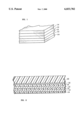
- FIG. 1 is a fragmentary schematic illustration, in perspective and on a greatly magnified scale, of a flake of magnetodielectric material made in accordance with the invention.
- FIG. 2 is a schematic illustration, in cross section and on a greatly magnified scale, of a method for making the flakes of the invention.
- FIG. 1 illustrates, diagrammatically and on an enlarged scale, a flake 10 of magnetodielectric material formed in accordance with one embodiment of the invention.
- the flake should be of a size less than 1,000 microns, and may suitably range in size from about 100 to about 500 microns or more.
- the flake may be comprised of either a single layer of magnetic material 12 or, as illustrated, a plurality of alternating layers of magnetic material 12 and insulating material 14.
- the magnetic materials to be used include many binary, ternary and multicompound materials in addition to the nickel-iron and nickel-iron-cobalt alloys cited in the Walser et al patent.
- Typical new materials include neodymium, praseodymium, terbium dysprosium, niobium, titanium, zirconium and other rare earth elements that provide either or both of greater magnetization and higher frequency response. Such materials may be used in various compounds with one another and/or iron, cobalt or molybdenum.
- the insulating materials preferably include silicon, polymers, and other materials that can be deposited simultaneously with and at the same speed as the magnetic layers.
- the thickness of the layers of both the magnetic material and the insulating material is in the range of from about 200 to about 5,000 angstroms (0.02 to 0.50 microns).
- the layers of insulating material are made as thin as feasible in order to enhance the effective volume fraction of magnetic material in the flakes.
- the number of layers of material in each flake may range from 1 (a single layer of magnetic material) to 100 or more.
- the total thickness of each flake may therefore range from about 0.02 microns to about 50 microns or more.
- the flakes 10 are manufactured by first forming a large sheet of material 12 or alternating layers of materials 12 and 14 and then breaking the sheet into particles and mechanically sizing the particles into flakes of the desired size.
- the sheet of magnetodielectric material is suitably formed, as illustrated diagrammatically in FIG. 2, by depositing a layer of material 12 or alternating layers of materials 12 and 14 onto a manufacturing substrate 30 that is coated with a layer 32 of water or solvent soluble release material, e.g., soap.
- the substrate may be a wide continuous sheet or film of a suitable polymer of the requisite strength, i.e., PET, in sheet or roll form, for purposes of continuous in-line processing.
- the layer first deposited onto the substrate 30 may be either one of the two materials, as desired, and the layer last deposited may likewise be either one of the two materials, as desired.
- the first and last layers be of insulating material 14 so that the conductive layers 12 are substantially encapsulated in insulation and will therefore eliminate conductive paths and prevent or greatly reduce DC conductivity in the composition when the flakes are dispersed in the binder.
- Deposition of the two materials is preferably carried out sequentially in a common vacuum chamber by sputter or vapor deposition, such as suggested by Walser et al or as taught in Meckel et al U.S. Pat. No. 4,322,276, Homstad et al. PCT/US89/01772 (Publication No. WO 89/10430, dated Nov. 2, 1989), Scobey et al. U.S. Pat. No. 4,851,095 and Yang U.S. Pat. No. 5,513,040.
- the insulating material 14 comprises a curable material that can be deposited by spraying or the like and then cured insitu by electron beam (E beam) or ultraviolet (UV) radiation, e.g., a polymer that is deposited in the form of a monomer or dimer and then polymerized insitu by E beam or UV radiation.
- E beam electron beam
- UV ultraviolet
- Apparatus for sputter or vapor deposition of the metal and for deposition and curing of a curable dielectric, in sequence in a common vacuum chamber are disclosed for example in Yializis et al. U.S. Pat. No. 4,842,893 and Yang U.S. Pat. No. 5,464,710.
- Such apparatus is readily adapted to practice of the present invention and provides a method for applying the two materials simultaneously in a single, continuous, in-line production operation.
- the substrate 30 is immersed in water or in an appropriate solvent to dissolve the release coat 32 and free the sheet of magnetodielectric material from the manufacturing substrate.
- the manufacturing substrate may then be conditioned for further use.
- the sheet of magnetodielectric material floated off the substrate 30 breaks into pieces or chunks which are filtered out of the solvent and dried.
- the pieces or chunks are then mechanically or ultrasonically reduced to flakes of the desired size by screening the same through sieves of selected sizes.
- sizing is achieved by dispersing the pieces or chunks of material in a high viscosity fluid and subjecting the pieces of material to high shear in a high shear mixer.
- the duration of mixing will in general determine the flake size.
- a high shear mixer will produce flakes having some size distribution, but such size distribution is found to be desirable so long as the flakes are of performance size.
- a degree of presizing of the pieces or particles into which the sheet of magnetodielectric material is broken may be attained by utilizing as the substrate 30 a film of material having a surface configuration like a waffle iron thereby to form a sheet of magnetodielectric material containing preselected lines of fracture.
- the magnetodielectric flakes 10 thus formed and sized are then mixed in an appropriate liquid or fluent binder at a concentration of from about 30% to about 60% by volume.
- the binder should preferably be dielectric, radio frequency transparent and easily set or cured.
- the composition thus formed may then be sprayed or brushed onto the surface of an article much like paint to impart magnetodielectric characteristics to the article.
- the composition may be cast or molded into sheets or structural magnetic components or elements.
- the preferred binder is polyurethane.
- other binders may be more suitable, such as epoxies, phenolics and polimides.
- cobalt based multi-layer magnetic flakes in epoxy would have a tensile modulus on the order of 10 million psi and a tensile strength of 50,000 psi, which is comparable to aluminum. Colorants may also be added to the composition for aesthetic purposes, if desired.
- the typical thickness of the coating or sheet will be on the order of 0.005 to 0.5 inches, depending upon the frequency or frequencies of interest.
- the invention thus provides a magnetodielectric material that, in comparison to the prior art, is lower in volume, lower in cost, lighter in weight and thinner, and at the same time has high electrical thickness, low reflection, low impedance and low attenuation loss. Because the supporting substrate and essential sheet formation of the prior art is eliminated by practice of the invention, the effective volume concentration of magnetic material in the composition is greatly increased and the number of uses and devices to which the composition is applicable are greatly broadened.
- the material of the invention is thinner, lighter, lower in cost and can be made into any arbitrary shape desired. The material will thus serve to reduce the size, weight and volume of electrical devices such as antennas, delay lines, phase shifters and other electrical devices requiring interaction with and/or magnetic response to high frequency radiation.
Landscapes
- Engineering & Computer Science (AREA)
- Power Engineering (AREA)
- Physics & Mathematics (AREA)
- Manufacturing & Machinery (AREA)
- General Physics & Mathematics (AREA)
- Optics & Photonics (AREA)
- Spectroscopy & Molecular Physics (AREA)
- Chemical & Material Sciences (AREA)
- Dispersion Chemistry (AREA)
- Powder Metallurgy (AREA)
Abstract
Description
Claims (12)
Priority Applications (1)
| Application Number | Priority Date | Filing Date | Title |
|---|---|---|---|
| US08/861,240 US6033782A (en) | 1993-08-13 | 1997-05-21 | Low volume lightweight magnetodielectric materials |
Applications Claiming Priority (3)
| Application Number | Priority Date | Filing Date | Title |
|---|---|---|---|
| US10648893A | 1993-08-13 | 1993-08-13 | |
| US08/349,957 US5814367A (en) | 1993-08-13 | 1994-12-06 | Broadband infrared and signature control materials and methods of producing the same |
| US08/861,240 US6033782A (en) | 1993-08-13 | 1997-05-21 | Low volume lightweight magnetodielectric materials |
Related Parent Applications (2)
| Application Number | Title | Priority Date | Filing Date |
|---|---|---|---|
| US10648893A Continuation-In-Part | 1993-08-13 | 1993-08-13 | |
| US08/349,957 Continuation-In-Part US5814367A (en) | 1993-08-13 | 1994-12-06 | Broadband infrared and signature control materials and methods of producing the same |
Publications (1)
| Publication Number | Publication Date |
|---|---|
| US6033782A true US6033782A (en) | 2000-03-07 |
Family
ID=46254482
Family Applications (1)
| Application Number | Title | Priority Date | Filing Date |
|---|---|---|---|
| US08/861,240 Expired - Lifetime US6033782A (en) | 1993-08-13 | 1997-05-21 | Low volume lightweight magnetodielectric materials |
Country Status (1)
| Country | Link |
|---|---|
| US (1) | US6033782A (en) |
Cited By (46)
| Publication number | Priority date | Publication date | Assignee | Title |
|---|---|---|---|---|
| US20010031549A1 (en) * | 1999-11-23 | 2001-10-18 | Crawford Ankur Mohan | Magnetic layer processing |
| US20020008605A1 (en) * | 1999-11-23 | 2002-01-24 | Gardner Donald S. | Integrated transformer |
| US20030005572A1 (en) * | 1999-11-23 | 2003-01-09 | Gardner Donald S. | Integrated inductor |
| US20040051297A1 (en) * | 2002-07-15 | 2004-03-18 | Flex Products, Inc., A Jds Uniphase Company | Method and apparatus for orienting magnetic flakes |
| US6753044B2 (en) | 1991-11-27 | 2004-06-22 | Reveo, Inc. | Coloring media having improved brightness and color characteristics |
| US20040151827A1 (en) * | 2002-09-13 | 2004-08-05 | Flex Products, Inc., A Jds Uniphase Company | Opaque flake for covert security applications |
| US20040157370A1 (en) * | 1999-11-23 | 2004-08-12 | Intel Corporation | Inductors for integrated circuits, integrated circuit components, and integrated circuit packages |
| US20040222492A1 (en) * | 2003-05-05 | 2004-11-11 | Gardner Donald S. | On-die micro-transformer structures with magnetic materials |
| US20050009846A1 (en) * | 2001-06-27 | 2005-01-13 | Fischer Peter Martin | 2,6,9-Substituted purine derivatives and their use in the treatment of proliferative disorders |
| US20050037192A1 (en) * | 2003-08-14 | 2005-02-17 | Flex Prodcuts, Inc., A Jds Uniphase Company | Flake for covert security applications |
| US6891461B2 (en) | 1999-11-23 | 2005-05-10 | Intel Corporation | Integrated transformer |
| US20050106367A1 (en) * | 2002-07-15 | 2005-05-19 | Jds Uniphase Corporation | Method and apparatus for orienting magnetic flakes |
| US6902807B1 (en) | 2002-09-13 | 2005-06-07 | Flex Products, Inc. | Alignable diffractive pigment flakes |
| US20050161630A1 (en) * | 2002-02-28 | 2005-07-28 | Siu-Tat Chui | Left handed materials using magnetic composites |
| US20060077496A1 (en) * | 1999-07-08 | 2006-04-13 | Jds Uniphase Corporation | Patterned structures with optically variable effects |
| US20060097515A1 (en) * | 2002-07-15 | 2006-05-11 | Jds Uniphase Corporation | Kinematic images formed by orienting alignable flakes |
| US20060119518A1 (en) * | 2003-02-18 | 2006-06-08 | Tadahiro Ohmi | Antenna for portable terminal and portable terminal using same |
| US20060194040A1 (en) * | 2002-09-13 | 2006-08-31 | Jds Uniphase Corporation | Two-step method of coating an article for security printing |
| US20060198998A1 (en) * | 2002-07-15 | 2006-09-07 | Jds Uniphase Corporation | Dynamic appearance-changing optical devices (dacod) printed in a shaped magnetic field including printable fresnel structures |
| US20060216453A1 (en) * | 2005-03-23 | 2006-09-28 | General Atomics | Durable pigmented film |
| US20060263539A1 (en) * | 2002-07-15 | 2006-11-23 | Jds Uniphase Corporation | Alignable Diffractive Pigment Flakes And Method And Apparatus For Alignment And Images Formed Therefrom |
| US20070001762A1 (en) * | 2005-06-30 | 2007-01-04 | Gerhard Schrom | DC-DC converter switching transistor current measurement technique |
| US20070139744A1 (en) * | 2002-09-13 | 2007-06-21 | Jds Uniphase Corporation | Security Device With Metameric Features Using Diffractive Pigment Flakes |
| US20070172261A1 (en) * | 2002-07-15 | 2007-07-26 | Jds Uniphase Corporation | Apparatus For Orienting Magnetic Flakes |
| US20070178293A1 (en) * | 2006-01-06 | 2007-08-02 | Yerkes Steven C | Super Lattice Intrinsic Materials |
| US20070183047A1 (en) * | 2000-01-21 | 2007-08-09 | Jds Uniphase Corporation | Optically Variable Security Devices |
| US20070188397A1 (en) * | 2006-02-13 | 2007-08-16 | Harris Corporation | Broadband polarized antenna including magnetodielectric material, isoimpedance loading, and associated methods |
| US7258900B2 (en) | 2002-07-15 | 2007-08-21 | Jds Uniphase Corporation | Magnetic planarization of pigment flakes |
| US20070195392A1 (en) * | 1999-07-08 | 2007-08-23 | Jds Uniphase Corporation | Adhesive Chromagram And Method Of Forming Thereof |
| US20080003413A1 (en) * | 2002-09-13 | 2008-01-03 | Jds Uniphase Corporation | Stamping A Coating Of Cured Field Aligned Special Effect Flakes And Image Formed Thereby |
| US20080019924A1 (en) * | 2003-08-14 | 2008-01-24 | Jds Uniphase Corporation | Non-Toxic Flakes For Authentication Of Pharmaceutical Articles |
| US20080024847A1 (en) * | 1999-07-08 | 2008-01-31 | Jds Uniphase Corporation | Patterned Optical Structures With Enhanced Security Feature |
| US20080107856A1 (en) * | 2002-09-13 | 2008-05-08 | Jds Uniphase Corporation | Provision of Frames Or Borders Around Pigment Flakes For Covert Security Applications |
| US20080171144A1 (en) * | 2002-09-13 | 2008-07-17 | Jds Uniphase Corporation | Printed Magnetic Ink Overt Security Image |
| US20090131130A1 (en) * | 2004-07-06 | 2009-05-21 | Seiko Epson Corporation | Electronic apparatus and wireless communication terminal |
| US7645510B2 (en) | 2002-09-13 | 2010-01-12 | Jds Uniphase Corporation | Provision of frames or borders around opaque flakes for covert security applications |
| US20100208351A1 (en) * | 2002-07-15 | 2010-08-19 | Nofi Michael R | Selective and oriented assembly of platelet materials and functional additives |
| US20110053359A1 (en) * | 2009-08-25 | 2011-03-03 | General Atomics | Methods of manufacturing quantum well materials |
| US8658280B2 (en) | 2002-09-13 | 2014-02-25 | Jds Uniphase Corporation | Taggent flakes for covert security applications having a selected shape |
| US9102195B2 (en) | 2012-01-12 | 2015-08-11 | Jds Uniphase Corporation | Article with curved patterns formed of aligned pigment flakes |
| US9458324B2 (en) | 2002-09-13 | 2016-10-04 | Viava Solutions Inc. | Flakes with undulate borders and method of forming thereof |
| US10343436B2 (en) | 2006-02-27 | 2019-07-09 | Viavi Solutions Inc. | Security device formed by printing with special effect inks |
| CN111247608A (en) * | 2017-10-27 | 2020-06-05 | 3M创新有限公司 | High-frequency power inductor material |
| WO2020219938A1 (en) * | 2019-04-24 | 2020-10-29 | Acs International Products, L. P. | Mesh flakes for use in compositions of resin and mesh or mesh-like materials |
| US11230127B2 (en) | 2002-07-15 | 2022-01-25 | Viavi Solutions Inc. | Method and apparatus for orienting magnetic flakes |
| US11768321B2 (en) | 2000-01-21 | 2023-09-26 | Viavi Solutions Inc. | Optically variable security devices |
Citations (20)
| Publication number | Priority date | Publication date | Assignee | Title |
|---|---|---|---|---|
| US3540047A (en) * | 1968-07-15 | 1970-11-10 | Conductron Corp | Thin film magnetodielectric materials |
| US4168986A (en) * | 1978-07-03 | 1979-09-25 | Polaroid Corporation | Method for preparing lamellar pigments |
| US4204942A (en) * | 1978-10-11 | 1980-05-27 | Heat Mirror Associates | Apparatus for multilayer thin film deposition |
| US4322276A (en) * | 1979-06-20 | 1982-03-30 | Deposition Technology, Inc. | Method for producing an inhomogeneous film for selective reflection/transmission of solar radiation |
| US4337990A (en) * | 1974-08-16 | 1982-07-06 | Massachusetts Institute Of Technology | Transparent heat-mirror |
| US4407685A (en) * | 1979-07-23 | 1983-10-04 | Ford Aerospace & Communication Corporation | Metallized film transfer process |
| US4414254A (en) * | 1980-12-26 | 1983-11-08 | Teijin Limited | Selective light-transmitting laminated structure |
| US4842893A (en) * | 1983-12-19 | 1989-06-27 | Spectrum Control, Inc. | High speed process for coating substrates |
| US4851095A (en) * | 1988-02-08 | 1989-07-25 | Optical Coating Laboratory, Inc. | Magnetron sputtering apparatus and process |
| WO1989010430A1 (en) * | 1988-04-27 | 1989-11-02 | American Thin Film Laboratories, Inc. | Vacuum coating system |
| US4923585A (en) * | 1988-11-02 | 1990-05-08 | Arch Development Corporation | Sputter deposition for multi-component thin films |
| US5051200A (en) * | 1989-09-19 | 1991-09-24 | The B. F. Goodrich Company | Flexible high energy magnetic blend compositions based on rare earth magnetic particles in highly saturated nitrile rubber |
| US5059245A (en) * | 1979-12-28 | 1991-10-22 | Flex Products, Inc. | Ink incorporating optically variable thin film flakes |
| US5366664A (en) * | 1992-05-04 | 1994-11-22 | The Penn State Research Foundation | Electromagnetic shielding materials |
| US5383995A (en) * | 1979-12-28 | 1995-01-24 | Flex Products, Inc. | Method of making optical thin flakes and inks incorporating the same |
| US5409624A (en) * | 1993-01-29 | 1995-04-25 | Ici Japan Limited | Bonded magnet moulding compositions |
| US5464710A (en) * | 1993-12-10 | 1995-11-07 | Deposition Technologies, Inc. | Enhancement of optically variable images |
| US5513040A (en) * | 1994-11-01 | 1996-04-30 | Deposition Technologies, Inc. | Optical device having low visual light transmission and low visual light reflection |
| US5571624A (en) * | 1979-12-28 | 1996-11-05 | Flex Products, Inc. | High chroma multilayer interference platelets |
| US5629092A (en) * | 1994-12-16 | 1997-05-13 | General Motors Corporation | Lubricous encapsulated ferromagnetic particles |
-
1997
- 1997-05-21 US US08/861,240 patent/US6033782A/en not_active Expired - Lifetime
Patent Citations (21)
| Publication number | Priority date | Publication date | Assignee | Title |
|---|---|---|---|---|
| US3540047A (en) * | 1968-07-15 | 1970-11-10 | Conductron Corp | Thin film magnetodielectric materials |
| US4337990A (en) * | 1974-08-16 | 1982-07-06 | Massachusetts Institute Of Technology | Transparent heat-mirror |
| US4168986A (en) * | 1978-07-03 | 1979-09-25 | Polaroid Corporation | Method for preparing lamellar pigments |
| US4204942A (en) * | 1978-10-11 | 1980-05-27 | Heat Mirror Associates | Apparatus for multilayer thin film deposition |
| US4322276A (en) * | 1979-06-20 | 1982-03-30 | Deposition Technology, Inc. | Method for producing an inhomogeneous film for selective reflection/transmission of solar radiation |
| US4407685A (en) * | 1979-07-23 | 1983-10-04 | Ford Aerospace & Communication Corporation | Metallized film transfer process |
| US5383995A (en) * | 1979-12-28 | 1995-01-24 | Flex Products, Inc. | Method of making optical thin flakes and inks incorporating the same |
| US5059245A (en) * | 1979-12-28 | 1991-10-22 | Flex Products, Inc. | Ink incorporating optically variable thin film flakes |
| US5571624A (en) * | 1979-12-28 | 1996-11-05 | Flex Products, Inc. | High chroma multilayer interference platelets |
| US4414254A (en) * | 1980-12-26 | 1983-11-08 | Teijin Limited | Selective light-transmitting laminated structure |
| US4842893A (en) * | 1983-12-19 | 1989-06-27 | Spectrum Control, Inc. | High speed process for coating substrates |
| US4851095A (en) * | 1988-02-08 | 1989-07-25 | Optical Coating Laboratory, Inc. | Magnetron sputtering apparatus and process |
| WO1989010430A1 (en) * | 1988-04-27 | 1989-11-02 | American Thin Film Laboratories, Inc. | Vacuum coating system |
| US4923585A (en) * | 1988-11-02 | 1990-05-08 | Arch Development Corporation | Sputter deposition for multi-component thin films |
| US5051200A (en) * | 1989-09-19 | 1991-09-24 | The B. F. Goodrich Company | Flexible high energy magnetic blend compositions based on rare earth magnetic particles in highly saturated nitrile rubber |
| US5366664A (en) * | 1992-05-04 | 1994-11-22 | The Penn State Research Foundation | Electromagnetic shielding materials |
| US5409624A (en) * | 1993-01-29 | 1995-04-25 | Ici Japan Limited | Bonded magnet moulding compositions |
| US5464710A (en) * | 1993-12-10 | 1995-11-07 | Deposition Technologies, Inc. | Enhancement of optically variable images |
| US5513040A (en) * | 1994-11-01 | 1996-04-30 | Deposition Technologies, Inc. | Optical device having low visual light transmission and low visual light reflection |
| US5513040B1 (en) * | 1994-11-01 | 1998-02-03 | Deposition Technology Inc | Optical device having low visual light transmission and low visual light reflection |
| US5629092A (en) * | 1994-12-16 | 1997-05-13 | General Motors Corporation | Lubricous encapsulated ferromagnetic particles |
Cited By (114)
| Publication number | Priority date | Publication date | Assignee | Title |
|---|---|---|---|---|
| US6753044B2 (en) | 1991-11-27 | 2004-06-22 | Reveo, Inc. | Coloring media having improved brightness and color characteristics |
| US20060077496A1 (en) * | 1999-07-08 | 2006-04-13 | Jds Uniphase Corporation | Patterned structures with optically variable effects |
| US7667895B2 (en) | 1999-07-08 | 2010-02-23 | Jds Uniphase Corporation | Patterned structures with optically variable effects |
| US20080024847A1 (en) * | 1999-07-08 | 2008-01-31 | Jds Uniphase Corporation | Patterned Optical Structures With Enhanced Security Feature |
| US20070195392A1 (en) * | 1999-07-08 | 2007-08-23 | Jds Uniphase Corporation | Adhesive Chromagram And Method Of Forming Thereof |
| US7876481B2 (en) | 1999-07-08 | 2011-01-25 | Jds Uniphase Corporation | Patterned optical structures with enhanced security feature |
| US7880943B2 (en) | 1999-07-08 | 2011-02-01 | Jds Uniphase Corporation | Patterned optical structures with enhanced security feature |
| US6870456B2 (en) | 1999-11-23 | 2005-03-22 | Intel Corporation | Integrated transformer |
| US6943658B2 (en) | 1999-11-23 | 2005-09-13 | Intel Corporation | Integrated transformer |
| US6815220B2 (en) * | 1999-11-23 | 2004-11-09 | Intel Corporation | Magnetic layer processing |
| US20090015363A1 (en) * | 1999-11-23 | 2009-01-15 | Gardner Donald S | Integrated transformer |
| US20040250411A1 (en) * | 1999-11-23 | 2004-12-16 | Gardner Donald S. | Integrated inductor |
| US20040046630A1 (en) * | 1999-11-23 | 2004-03-11 | Gardner Donald S. | Integrated transformer |
| US6856228B2 (en) | 1999-11-23 | 2005-02-15 | Intel Corporation | Integrated inductor |
| US6856226B2 (en) | 1999-11-23 | 2005-02-15 | Intel Corporation | Integrated transformer |
| US7434306B2 (en) | 1999-11-23 | 2008-10-14 | Intel Corporation | Integrated transformer |
| US20020008605A1 (en) * | 1999-11-23 | 2002-01-24 | Gardner Donald S. | Integrated transformer |
| US20050062575A1 (en) * | 1999-11-23 | 2005-03-24 | Gardner Donald S. | Integrated transformer |
| US6891461B2 (en) | 1999-11-23 | 2005-05-10 | Intel Corporation | Integrated transformer |
| US20010031549A1 (en) * | 1999-11-23 | 2001-10-18 | Crawford Ankur Mohan | Magnetic layer processing |
| US7332792B2 (en) * | 1999-11-23 | 2008-02-19 | Intel Corporation | Magnetic layer processing |
| US20050146411A1 (en) * | 1999-11-23 | 2005-07-07 | Gardner Donald S. | Integrated inductor |
| US20040157370A1 (en) * | 1999-11-23 | 2004-08-12 | Intel Corporation | Inductors for integrated circuits, integrated circuit components, and integrated circuit packages |
| US6940147B2 (en) * | 1999-11-23 | 2005-09-06 | Intel Corporation | Integrated inductor having magnetic layer |
| US7982574B2 (en) | 1999-11-23 | 2011-07-19 | Intel Corporation | Integrated transformer |
| US6988307B2 (en) | 1999-11-23 | 2006-01-24 | Intel Corporation | Method of making an integrated inductor |
| US20030005572A1 (en) * | 1999-11-23 | 2003-01-09 | Gardner Donald S. | Integrated inductor |
| US7327010B2 (en) | 1999-11-23 | 2008-02-05 | Intel Corporation | Inductors for integrated circuits |
| US20030001713A1 (en) * | 1999-11-23 | 2003-01-02 | Gardner Donald S. | Integrated transformer |
| US7791447B2 (en) | 1999-11-23 | 2010-09-07 | Intel Corporation | Integrated transformer |
| US7064646B2 (en) | 1999-11-23 | 2006-06-20 | Intel Corporation | Integrated inductor |
| US20060163695A1 (en) * | 1999-11-23 | 2006-07-27 | Intel Corporation | Inductors for integrated circuits |
| US7087976B2 (en) | 1999-11-23 | 2006-08-08 | Intel Corporation | Inductors for integrated circuits |
| US7119650B2 (en) | 1999-11-23 | 2006-10-10 | Intel Corporation | Integrated transformer |
| US7299537B2 (en) | 1999-11-23 | 2007-11-27 | Intel Corporation | Method of making an integrated inductor |
| US20100295649A1 (en) * | 1999-11-23 | 2010-11-25 | Gardner Donald S | Integrated transformer |
| US11768321B2 (en) | 2000-01-21 | 2023-09-26 | Viavi Solutions Inc. | Optically variable security devices |
| US20070183047A1 (en) * | 2000-01-21 | 2007-08-09 | Jds Uniphase Corporation | Optically Variable Security Devices |
| US20050009846A1 (en) * | 2001-06-27 | 2005-01-13 | Fischer Peter Martin | 2,6,9-Substituted purine derivatives and their use in the treatment of proliferative disorders |
| US9257059B2 (en) | 2001-07-31 | 2016-02-09 | Viavi Solutions Inc. | Dynamic appearance-changing optical devices (DACOD) printed in a shaped magnetic field including printable fresnel structures |
| US20050161630A1 (en) * | 2002-02-28 | 2005-07-28 | Siu-Tat Chui | Left handed materials using magnetic composites |
| US20070172261A1 (en) * | 2002-07-15 | 2007-07-26 | Jds Uniphase Corporation | Apparatus For Orienting Magnetic Flakes |
| US7934451B2 (en) | 2002-07-15 | 2011-05-03 | Jds Uniphase Corporation | Apparatus for orienting magnetic flakes |
| US8343615B2 (en) | 2002-07-15 | 2013-01-01 | Jds Uniphase Corporation | Dynamic appearance-changing optical devices (DACOD) printed in a shaped magnetic field including printable fresnel structures |
| US20040051297A1 (en) * | 2002-07-15 | 2004-03-18 | Flex Products, Inc., A Jds Uniphase Company | Method and apparatus for orienting magnetic flakes |
| US8726806B2 (en) | 2002-07-15 | 2014-05-20 | Jds Uniphase Corporation | Apparatus for orienting magnetic flakes |
| US7258900B2 (en) | 2002-07-15 | 2007-08-21 | Jds Uniphase Corporation | Magnetic planarization of pigment flakes |
| US20060263539A1 (en) * | 2002-07-15 | 2006-11-23 | Jds Uniphase Corporation | Alignable Diffractive Pigment Flakes And Method And Apparatus For Alignment And Images Formed Therefrom |
| US9027479B2 (en) | 2002-07-15 | 2015-05-12 | Jds Uniphase Corporation | Method and apparatus for orienting magnetic flakes |
| US20060198998A1 (en) * | 2002-07-15 | 2006-09-07 | Jds Uniphase Corporation | Dynamic appearance-changing optical devices (dacod) printed in a shaped magnetic field including printable fresnel structures |
| US9522402B2 (en) | 2002-07-15 | 2016-12-20 | Viavi Solutions Inc. | Method and apparatus for orienting magnetic flakes |
| US20100208351A1 (en) * | 2002-07-15 | 2010-08-19 | Nofi Michael R | Selective and oriented assembly of platelet materials and functional additives |
| US7047883B2 (en) | 2002-07-15 | 2006-05-23 | Jds Uniphase Corporation | Method and apparatus for orienting magnetic flakes |
| US20060097515A1 (en) * | 2002-07-15 | 2006-05-11 | Jds Uniphase Corporation | Kinematic images formed by orienting alignable flakes |
| US10059137B2 (en) | 2002-07-15 | 2018-08-28 | Viavi Solutions Inc. | Apparatus for orienting magnetic flakes |
| US20050106367A1 (en) * | 2002-07-15 | 2005-05-19 | Jds Uniphase Corporation | Method and apparatus for orienting magnetic flakes |
| US7604855B2 (en) | 2002-07-15 | 2009-10-20 | Jds Uniphase Corporation | Kinematic images formed by orienting alignable flakes |
| US10173455B2 (en) | 2002-07-15 | 2019-01-08 | Viavi Solutions Inc. | Dynamic appearance-changing optical devices (DACOD) printed in a shaped magnetic field including printable fresnel structures |
| US11230127B2 (en) | 2002-07-15 | 2022-01-25 | Viavi Solutions Inc. | Method and apparatus for orienting magnetic flakes |
| US7517578B2 (en) | 2002-07-15 | 2009-04-14 | Jds Uniphase Corporation | Method and apparatus for orienting magnetic flakes |
| US20080107856A1 (en) * | 2002-09-13 | 2008-05-08 | Jds Uniphase Corporation | Provision of Frames Or Borders Around Pigment Flakes For Covert Security Applications |
| US20080003413A1 (en) * | 2002-09-13 | 2008-01-03 | Jds Uniphase Corporation | Stamping A Coating Of Cured Field Aligned Special Effect Flakes And Image Formed Thereby |
| US20040151827A1 (en) * | 2002-09-13 | 2004-08-05 | Flex Products, Inc., A Jds Uniphase Company | Opaque flake for covert security applications |
| US6902807B1 (en) | 2002-09-13 | 2005-06-07 | Flex Products, Inc. | Alignable diffractive pigment flakes |
| US20100002275A9 (en) * | 2002-09-13 | 2010-01-07 | Jds Uniphase Corporation | Security Device With Metameric Features Using Diffractive Pigment Flakes |
| US7645510B2 (en) | 2002-09-13 | 2010-01-12 | Jds Uniphase Corporation | Provision of frames or borders around opaque flakes for covert security applications |
| US20080171144A1 (en) * | 2002-09-13 | 2008-07-17 | Jds Uniphase Corporation | Printed Magnetic Ink Overt Security Image |
| US7674501B2 (en) | 2002-09-13 | 2010-03-09 | Jds Uniphase Corporation | Two-step method of coating an article for security printing by application of electric or magnetic field |
| US20070139744A1 (en) * | 2002-09-13 | 2007-06-21 | Jds Uniphase Corporation | Security Device With Metameric Features Using Diffractive Pigment Flakes |
| US7729026B2 (en) | 2002-09-13 | 2010-06-01 | Jds Uniphase Corporation | Security device with metameric features using diffractive pigment flakes |
| US8025952B2 (en) | 2002-09-13 | 2011-09-27 | Jds Uniphase Corporation | Printed magnetic ink overt security image |
| US8118963B2 (en) | 2002-09-13 | 2012-02-21 | Alberto Argoitia | Stamping a coating of cured field aligned special effect flakes and image formed thereby |
| US7300695B2 (en) | 2002-09-13 | 2007-11-27 | Jds Uniphase Corporation | Alignable diffractive pigment flakes |
| US9458324B2 (en) | 2002-09-13 | 2016-10-04 | Viava Solutions Inc. | Flakes with undulate borders and method of forming thereof |
| US20060194040A1 (en) * | 2002-09-13 | 2006-08-31 | Jds Uniphase Corporation | Two-step method of coating an article for security printing |
| USRE45762E1 (en) | 2002-09-13 | 2015-10-20 | Jds Uniphase Corporation | Printed magnetic ink overt security image |
| US9164575B2 (en) | 2002-09-13 | 2015-10-20 | Jds Uniphase Corporation | Provision of frames or borders around pigment flakes for covert security applications |
| US8999616B2 (en) | 2002-09-13 | 2015-04-07 | Jds Uniphase Corporation | Taggent flakes for covert security applications having a selected shape |
| US8658280B2 (en) | 2002-09-13 | 2014-02-25 | Jds Uniphase Corporation | Taggent flakes for covert security applications having a selected shape |
| US7241489B2 (en) | 2002-09-13 | 2007-07-10 | Jds Uniphase Corporation | Opaque flake for covert security applications |
| US7995001B2 (en) * | 2003-02-18 | 2011-08-09 | Tadahiro Ohmi | Antenna for portable terminal and portable terminal using same |
| US20060119518A1 (en) * | 2003-02-18 | 2006-06-08 | Tadahiro Ohmi | Antenna for portable terminal and portable terminal using same |
| CN1751415B (en) * | 2003-02-18 | 2010-05-05 | 大见忠弘 | Antenna for portable terminal and portable terminal using same |
| US8471667B2 (en) | 2003-05-05 | 2013-06-25 | Intel Corporation | On-die micro-transformer structures with magnetic materials |
| US20040222492A1 (en) * | 2003-05-05 | 2004-11-11 | Gardner Donald S. | On-die micro-transformer structures with magnetic materials |
| US7852185B2 (en) | 2003-05-05 | 2010-12-14 | Intel Corporation | On-die micro-transformer structures with magnetic materials |
| US20110068887A1 (en) * | 2003-05-05 | 2011-03-24 | Gardner Donald S | On-die micro-transformer structures with magnetic materials |
| US7258915B2 (en) | 2003-08-14 | 2007-08-21 | Jds Uniphase Corporation | Flake for covert security applications |
| US20050037192A1 (en) * | 2003-08-14 | 2005-02-17 | Flex Prodcuts, Inc., A Jds Uniphase Company | Flake for covert security applications |
| US7550197B2 (en) | 2003-08-14 | 2009-06-23 | Jds Uniphase Corporation | Non-toxic flakes for authentication of pharmaceutical articles |
| US20080019924A1 (en) * | 2003-08-14 | 2008-01-24 | Jds Uniphase Corporation | Non-Toxic Flakes For Authentication Of Pharmaceutical Articles |
| US8103319B2 (en) * | 2004-07-06 | 2012-01-24 | Seiko Epson Corporation | Electronic apparatus and wireless communication terminal |
| US20090131130A1 (en) * | 2004-07-06 | 2009-05-21 | Seiko Epson Corporation | Electronic apparatus and wireless communication terminal |
| US20060216453A1 (en) * | 2005-03-23 | 2006-09-28 | General Atomics | Durable pigmented film |
| US20070001762A1 (en) * | 2005-06-30 | 2007-01-04 | Gerhard Schrom | DC-DC converter switching transistor current measurement technique |
| US8134548B2 (en) | 2005-06-30 | 2012-03-13 | Micron Technology, Inc. | DC-DC converter switching transistor current measurement technique |
| US8482552B2 (en) | 2005-06-30 | 2013-07-09 | Micron Technology, Inc. | DC-DC converter switching transistor current measurement technique |
| US9124174B2 (en) | 2005-06-30 | 2015-09-01 | Micron Technology, Inc. | DC-DC converter switching transistor current measurement technique |
| US20120196097A1 (en) * | 2006-01-06 | 2012-08-02 | Yerkes Steven C | Super lattice intrinsic materials |
| US20070178293A1 (en) * | 2006-01-06 | 2007-08-02 | Yerkes Steven C | Super Lattice Intrinsic Materials |
| US20070188397A1 (en) * | 2006-02-13 | 2007-08-16 | Harris Corporation | Broadband polarized antenna including magnetodielectric material, isoimpedance loading, and associated methods |
| US7573431B2 (en) * | 2006-02-13 | 2009-08-11 | Harris Corporation | Broadband polarized antenna including magnetodielectric material, isoimpedance loading, and associated methods |
| US11504990B2 (en) | 2006-02-27 | 2022-11-22 | Viavi Solutions Inc. | Security device formed by printing with special effect inks |
| US10343436B2 (en) | 2006-02-27 | 2019-07-09 | Viavi Solutions Inc. | Security device formed by printing with special effect inks |
| US20110053359A1 (en) * | 2009-08-25 | 2011-03-03 | General Atomics | Methods of manufacturing quantum well materials |
| US8242348B2 (en) | 2009-08-25 | 2012-08-14 | General Atomics | Methods of manufacturing quantum well materials |
| US10232660B2 (en) | 2012-01-12 | 2019-03-19 | Viavi Solutions Inc. | Article with curved patterns formed of aligned pigment flakes |
| US10752042B2 (en) | 2012-01-12 | 2020-08-25 | Viavi Solutions Inc. | Article with dynamic frame formed with aligned pigment flakes |
| US11198315B2 (en) | 2012-01-12 | 2021-12-14 | Viavi Solutions Inc. | Article with curved patterns formed of aligned pigment flakes |
| US10562333B2 (en) | 2012-01-12 | 2020-02-18 | Viavi Solutions Inc. | Article with curved patterns formed of aligned pigment flakes |
| US10259254B2 (en) | 2012-01-12 | 2019-04-16 | Viavi Solutions Inc. | Article with a dynamic frame formed with aligned pigment flakes |
| US9102195B2 (en) | 2012-01-12 | 2015-08-11 | Jds Uniphase Corporation | Article with curved patterns formed of aligned pigment flakes |
| CN111247608A (en) * | 2017-10-27 | 2020-06-05 | 3M创新有限公司 | High-frequency power inductor material |
| WO2020219938A1 (en) * | 2019-04-24 | 2020-10-29 | Acs International Products, L. P. | Mesh flakes for use in compositions of resin and mesh or mesh-like materials |
Similar Documents
| Publication | Publication Date | Title |
|---|---|---|
| US6033782A (en) | Low volume lightweight magnetodielectric materials | |
| EP1213338B1 (en) | Methods for preparing flakes | |
| US5814367A (en) | Broadband infrared and signature control materials and methods of producing the same | |
| DE69913982T2 (en) | METHOD FOR PRODUCING METAL SHEETS | |
| US20060226399A1 (en) | Conductive flakes manufactured by combined sputtering and vapor deposition | |
| US5304274A (en) | Method for manufacturing electrodes for multilayer ceramic capacitors | |
| DE2453035B2 (en) | Method for applying a metallic layer in the form of a pattern on an inert substrate coated with a first thin metallic layer | |
| DE2616394C3 (en) | Process for the production of superconducting material consisting of a plastic or glass matrix with embedded particles | |
| US4732717A (en) | Process for producing piezo-electric or pyro-electric composite sheet | |
| DE2260043C3 (en) | Magnetic disk storage device and method for its manufacture | |
| DE4223887A1 (en) | Process for producing a polymer / metal or polymer / semiconductor composite | |
| US4839463A (en) | Ultra fine polymer particle and composite material of preparation for methods | |
| DE112012007173T5 (en) | Metal-coated film, intermediate for their production and related manufacturing process | |
| DE2736006A1 (en) | METHOD OF DEPOSITING THIN HAFNIUM LAYERS | |
| DE102015113542B4 (en) | Method for forming a layer with high light transmission and / or low light reflection | |
| JPS6197657A (en) | Manufacture of screen layer for xerographic material | |
| US2880181A (en) | Binder for conductive metallic film | |
| EP1470933A2 (en) | Protective layer comprising lacquer | |
| DE69814125T2 (en) | AMORPHE, HYDRATED, AROMATIC, THERMOPLASTIC SUBSTRATES WITH IMPROVED LIABILITY | |
| Skjeltorp | Fracture experiments on monolayers of microspheres | |
| EP2420587B1 (en) | Method for producing a coloured coating using cathodic sputtering | |
| KR100302583B1 (en) | Magnetostrictive Tb-Dy-Fe Alloy Composites and Manufacture Thereof | |
| DE2131513A1 (en) | Composite | |
| DE2447066A1 (en) | PHOTOCELL AND METHOD OF MANUFACTURING IT | |
| DE760147C (en) | Molded compound for the production of impact-resistant insulating molded bodies, especially for the purposes of high-frequency technology |
Legal Events
| Date | Code | Title | Description |
|---|---|---|---|
| AS | Assignment |
Owner name: GENERAL ATOMICS, CALIFORNIA Free format text: ASSIGNMENT OF ASSIGNORS INTEREST;ASSIGNORS:HUBBARD, RONALD N.;DUHL, MICHAEL L.;REEL/FRAME:008576/0111 Effective date: 19970513 |
|
| STCF | Information on status: patent grant |
Free format text: PATENTED CASE |
|
| FEPP | Fee payment procedure |
Free format text: PAYOR NUMBER ASSIGNED (ORIGINAL EVENT CODE: ASPN); ENTITY STATUS OF PATENT OWNER: LARGE ENTITY |
|
| FPAY | Fee payment |
Year of fee payment: 4 |
|
| FEPP | Fee payment procedure |
Free format text: PAYER NUMBER DE-ASSIGNED (ORIGINAL EVENT CODE: RMPN); ENTITY STATUS OF PATENT OWNER: LARGE ENTITY |
|
| FPAY | Fee payment |
Year of fee payment: 8 |
|
| REMI | Maintenance fee reminder mailed | ||
| REMI | Maintenance fee reminder mailed | ||
| FPAY | Fee payment |
Year of fee payment: 12 |
|
| SULP | Surcharge for late payment |
Year of fee payment: 11 |
|
| AS | Assignment |
Owner name: BANK OF THE WEST, CALIFORNIA Free format text: PATENT SECURITY AGREEMENT;ASSIGNOR:GENERAL ATOMICS;REEL/FRAME:042914/0365 Effective date: 20170620 |