US5974495A - Using a back-off signal to bridge a first bus to a second bus - Google Patents

Using a back-off signal to bridge a first bus to a second bus Download PDF

Info

Publication number
US5974495A
US5974495A US09/087,229 US8722998A US5974495A US 5974495 A US5974495 A US 5974495A US 8722998 A US8722998 A US 8722998A US 5974495 A US5974495 A US 5974495A
Authority
US
United States
Prior art keywords
bus
cycle
signal
pci
bus cycle
Prior art date
Legal status (The legal status is an assumption and is not a legal conclusion. Google has not performed a legal analysis and makes no representation as to the accuracy of the status listed.)
Expired - Lifetime
Application number
US09/087,229
Inventor
Fong Lu (David) Lin
Cherng-Yeuan (Henry) Tsay
David H. Doan
Current Assignee (The listed assignees may be inaccurate. Google has not performed a legal analysis and makes no representation or warranty as to the accuracy of the list.)
OPTi Inc
Original Assignee
OPTi Inc
Priority date (The priority date is an assumption and is not a legal conclusion. Google has not performed a legal analysis and makes no representation as to the accuracy of the date listed.)
Filing date
Publication date
Application filed by OPTi Inc filed Critical OPTi Inc
Priority to US09/087,229 priority Critical patent/US5974495A/en
Priority to JP15032199A priority patent/JP2000138917A/en
Application granted granted Critical
Publication of US5974495A publication Critical patent/US5974495A/en
Anticipated expiration legal-status Critical
Expired - Lifetime legal-status Critical Current

Links

Images

Classifications

    • GPHYSICS
    • G06COMPUTING; CALCULATING OR COUNTING
    • G06FELECTRIC DIGITAL DATA PROCESSING
    • G06F21/00Security arrangements for protecting computers, components thereof, programs or data against unauthorised activity
    • GPHYSICS
    • G06COMPUTING; CALCULATING OR COUNTING
    • G06FELECTRIC DIGITAL DATA PROCESSING
    • G06F13/00Interconnection of, or transfer of information or other signals between, memories, input/output devices or central processing units
    • G06F13/38Information transfer, e.g. on bus
    • G06F13/40Bus structure
    • G06F13/4004Coupling between buses
    • G06F13/4027Coupling between buses using bus bridges
    • G06F13/405Coupling between buses using bus bridges where the bridge performs a synchronising function
    • GPHYSICS
    • G06COMPUTING; CALCULATING OR COUNTING
    • G06FELECTRIC DIGITAL DATA PROCESSING
    • G06F2207/00Indexing scheme relating to methods or arrangements for processing data by operating upon the order or content of the data handled
    • G06F2207/72Indexing scheme relating to groups G06F7/72 - G06F7/729
    • G06F2207/7219Countermeasures against side channel or fault attacks

Definitions

  • the invention relates to IBM PC AT-compatible computer architectures, and more particularly, to enhancements thereof for communicating with I/O peripheral devices.
  • the IBM PC/AT® computer architecture has become an industry standard architecture for personal computers and is typically built around a host CPU such as an 80386, 80486 or Pentium® microprocessor manufactured by Intel Corporation, or similar microprocessors manufactured by others.
  • the host CPU is coupled to a host bus, capable of performing memory accesses and data transfers at high rates of speed (i.e., on the order of 25-100 MHz with today's technology).
  • the host bus includes 32 or, in the case of computers built around the Pentium, 64 data lines, a plurality of address lines, and various control lines.
  • the typical IBM PC AT-compatible platform also includes DRAM main memory, and in many cases a timer, a real-time clock, and a cache memory.
  • the typical IBM PC AT-compatible computer also includes an I/O bus, also know as a system bus or AT-bus, which is separate and distinct from the host bus.
  • the system bus usually conforms to one of two industry-established standards known as ISA (Industry Standard Architecture) and EISA (Extended ISA).
  • ISA Industry Standard Architecture
  • EISA Extended ISA
  • the system bus is coupled to the host bus via a host-bus/system-bus bridge, and includes, depending on the system bus standard adhered to, 16 or 32 data lines, a plurality of address lines, as well as control lines.
  • the I/O address space is logically distinct from the memory address space and if the CPU desires to access an I/O address, it does so by executing a special I/O instruction.
  • Such an I/O instruction generates memory access signals on the host bus, but also activates an M/IO# signal on the host bus to indicate that this is an access to the I/O address space.
  • the host-bus/system-bus bridge recognizes the I/O signals thereby generated by the CPU, performs the desired operation over the system bus, and if appropriate, returns results to the CPU over the host bus.
  • I/O addresses may reside physically on the host bus and some memory addresses may reside physically on the system bus. More specifically, the devices which respond to accesses to certain I/O space addresses may be connected to the control lines (and usually the address and data lines as well) of the host bus, while the devices which respond to accesses to certain memory space addresses may be connected to the control lines (and usually the address and data lines as well) of the system bus.
  • the host-bus/system-bus bridge is responsible for recognizing that a memory or I/O address access must be emulated by an access to the other bus, and is responsible for doing such emulation.
  • a ROM (or EPROM) BIOS may reside physically on the system bus, but actually form part of the local memory address space.
  • the host-bus/system-bus bridge recognizes such, enables a buffer (considered herein as being part of the host-bus/system-bus bridge) which couples the address onto the system bus, and activates the chip select for the ROM.
  • the bridge then assembles a data word of the size expected by the host CPU, from the data returned by the ROM, and couples the word onto the host bus for receipt by the CPU.
  • the ROM BIOS is copied into equivalent locations in the DRAM main memory, which does reside on the host bus, and thereafter accessed directly.
  • the logical main memory address space is divided into a low memory range (0h-9FFFFh), a reserved memory range (A0000h-FFFFFh) and an extended memory range (10000h to the top of memory).
  • system ROM BIOS is located logically at memory space addresses F0000h FFFFFh, and resides physically on the system bus. Addresses C0000h-EFFFFh contain ROM BIOS portions for specific add-on cards and reside physically on their respective cards on the system bus. Addresses A0000h-BFFFFh contain the video buffer, which is a part of a video controller residing on the system bus.
  • Duplicate memory space is typically provided in DRAM on the host bus for addresses C0000h-FFFFFh, and the user of the system can select during a setup procedure, which portions of the ROM BIOS are to be "shadowed" by being copied into the duplicate DRAM space during boot-up.
  • a keyboard controller typically also resides on the system bus, as does the timer and real-time clock.
  • a typical IBM PC AT-compatible system may also include a DMA controller which permits peripheral devices on the system bus to read or write directly to or from main memory, as well as an interrupt controller for transmitting interrupts from various add-on cards to the CPU.
  • the add-on cards are cards which may be plugged into slot connectors coupled to the system bus to increase the capabilities of the system. Add-on cards are also sometimes referred to as expansion cards or accessory cards.
  • the various signals on the host bus include the input/output signals of whichever microprocessor the system is built around. Such signals are therefore well known in the industry and can be determined by reference to the above-incorporated publications.
  • the various signals on the system bus also are well known in the industry.
  • the Solari book incorporated above describes the lines in detail. For present purposes, only the following signals are important:
  • signals which are asserted low are given a ⁇ # ⁇ or ⁇ B ⁇ suffix in their names, whereas those asserted high (or for which an assertion polarity has no meaning) lack a ⁇ # ⁇ or ⁇ B ⁇ suffix.
  • two signal names mentioned herein that are identical except that one includes the ⁇ # ⁇ or ⁇ B ⁇ suffix while the other omits it are intended to represent logical compliments of the same signal. It will be understood that one can be generated by inverting the other, or both can be generated by separate logic in response to common predecessor signals.
  • PC AT chipsets also known as “core logic chipsets” or "I/O bus interface circuitry"
  • I/O bus interface circuitry An example of such a chipset is the 386WB PC/AT chipset manufactured by OPTi, Inc., Santa Clara, Calif.
  • These chipsets implement the host-bus/system bus bridge, the timer, real-time clock (RTC), DMA controller, as well as some additional functionality.
  • the host-bus/system-bus bridge circuitry needs to delay its handling of requests and responses from one bus to the other merely because the clocks are not synchronized. The circuitry therefore must hold a request or response until the appropriate clock edge on the destination bus appears. This can add on the order of 30-200 nS to each system bus cycle. Accordingly, it can be seen that any access to a peripheral device on the system bus imposes a substantial penalty on the performance of PC AT-compatible computers. This penalty will only become worse as the disparity between the host bus and system bus data rates continues to increase.
  • Video display controllers have a command port which responds to accesses in the I/O address space, as well as a video memory port which responds to accesses in the memory address space.
  • Manufacturers have traditionally placed both ports on the system bus, however, thereby imposing the speed limitations of the system bus on the video memory port as well as the command port.
  • OPTI3030WSW owned by the assignee of the present application and incorporated herein by reference in its entirety, describes certain attempts to permit accesses to the video memory port to take place over the host bus instead of the system bus.
  • some graphics chip vendors have tried incorporating features into their chips for connection directly to a host bus.
  • VL-Bus Video Electronics Standards Association
  • VL-Bus Video Electronics Standards Association
  • VL-Bus VL-Bus Local Bus Standard
  • VL-Bus VL-Bus Local Bus Standard
  • Significant aspects of the VL-Bus specifications are described in Appendix A hereto. Further revisions of the VESA standard are in preparation, one recent version being VESA, "VESA VL-Bus Proposal, Version 2.0p, Revision 0.8p (May 17, 1993), also incorporated herein by reference.
  • PCI PCI 2.0 Bus specifications
  • Intel Corp. "Peripheral Component Interconnect (PCI), revision 1.0 Specification” (Jun. 22, 1992) and in PCI Special Interest Group, "PCI Local Bus Specification", Revision 2.0 (Apr. 30, 1993), both incorporated herein by reference.
  • PCI 2.0 Bus specifications are described in Appendix B hereto.
  • VL-bus is relatively simple to include in a personal computer system, especially those built around an Intel 486 microprocessor. This is because the VL-bus signal lines are similar to signal lines of the 486 CPU, except for a few additional signal lines included on the VL-bus. Thus the only additional expense required to add a VL-bus to a pre-existing 486-based computer design, is a very small VL-bus controller to handle the additional signal lines. Such a controller has already been included in chipsets. An example of such a chipset includes the OPTi 82C802G and either the 82C601 or 82C602, all incorporated herein by reference.
  • the 82C802G is described in OPTi, Inc., "OPTi PC/AT Single Chip 82C802G Data Book", Version 1.2a (Dec. 1, 1993), and significant aspects are also set forth in Appendix C hereto.
  • the 82C601 and 82C602 are described in OPTi, Inc., "PC/AT Data Buffer Chips, Preliminary, 82C601/82C602 Data Book", Version 1.0e (Oct. 13, 1993), and significant aspects are also set forth in Appendix D hereto. Both data books are incorporated herein by reference in their entirety.
  • VL-bus/VL-bus bridge While a minimum VL-bus system requires no additional circuitry, the insertion of a simple host-bus/VL-bus bridge provides buffering for additional VL-bus devices.
  • the bridge could also include circuitry to break up a 64-bit host-bus originated access, into two 32-bit VL-bus accesses. Such circuitry is still relatively simple.
  • PCI-bus A primary advantage of the PCI-bus, on the other hand, is its processor independence.
  • the PCI-bus was intended to provide very high-speed accesses using a standard bus protocol, and to interface those accesses with any host processor bus using an appropriate host-bus/PCI-bus bridge.
  • the host-bus/PCI-bus bridge is significantly more expensive than the circuitry required to implement a VL-bus, but the independence it provides from ever-faster and ever-more varied host processor buses provides a stable target for designers of peripheral products.
  • a peripheral device designed for the PCI-bus would not need to be redesigned for each new version of an Intel microprocessor, or indeed, for each new microprocessor that might in the future power a personal computer system.
  • the motherboard circuitry to implement this would be expected to include programmable registers which would indicate whether a particular valid cycle definition on the host bus is to be handled by a device on the host bus (such as main memory), a device on the VL-bus (which may be the same as the host bus in 486 systems), by a device on the PCI-bus, or by a device on the system bus.
  • a device on the host bus such as main memory
  • a device on the VL-bus which may be the same as the host bus in 486 systems
  • a device on the PCI-bus or by a device on the system bus.
  • Such motherboard circuitry would be expensive, however, and may require an entirely new chipset design.
  • VL-bus/PCI-bus bridge chip which, together with the Acer M1429kG/M1429 VESA chip, permits both a VL-bus and a PCI-bus to be included in a single system.
  • the M1435 chip detects a valid VL-bus cycle, it first determines whether the cycle is intended for system memory or for another VL-bus device.
  • the chip is believed to perform a positive decode of the address to determine whether the cycle is intended for system memory, and it observes the LDEV signal to determine whether the cycle has been claimed by another VL-bus device. If neither is the case, then the M1435 translates the cycle to the PCI-bus. If no PCI agent claims the translated PCI cycle, then the M1435 asserts an ISA REQJ signal to the M1429 chip, thereby informing the M1429 to start an ISA cycle. See also Acer Laboratories, Inc., "M1429G/M1431/M1435 Data Sheet” (October 1993), incorporated herein by reference.
  • the Acer technique for accommodating both the VL-bus and PCI-bus in a single system is limited in that it operates only with a host-bus/system-bus interface chipset which observes and understands the ISA REQJ signal asserted by the M1435 bridge.
  • Other inter-chip signals may also be required between the M1435 and M1429. Since most interface chipsets do not understand these signals, such chipsets would have to be modified by the chipset manufacturer before they could be used with the M1435 bridge. It would be desirable, therefore, to provide a VL-bus/PCI-bus bridge which does not require modification of any existing VL-bus/system-bus chipset. Such a bridge could be used in conjunction with the chipset of any manufacturer which supports the VL-bus.
  • the invention takes advantage of a feature of Intel 486 and Pentium microprocessors, known as the back-off feature. These microprocessors sense a BOFF# signal, which is not considered part of the VL-bus. When the microprocessor detects assertion of BOFF#, while a host bus cycle is in progress, it aborts the cycle and restarts it after it detects BOFF# negated. According to the invention, roughly described, a VL-bus/PCI-bus bridge claims a VL-bus cycle by asserting LDEV# to the VL-bus/system-bus bridge.
  • the VL-bus/PCI-bus bridge translates the cycle onto the PCI-bus and awaits a response from a PCI device. If no PCI device claims a cycle by the PCI-bus device claiming deadline, then the bridge asserts BOFF# to the host. The bridge then awaits the host's repetition of the cycle which was subject to the BOFF#, and suppresses its assertion of LDEV# so that the VL-bus/system-bus bridge can translate the cycle onto the system bus.
  • a VL-bus device can take advantage of the back-off feature of the 486 and Pentium CPU's by asserting the VL-bus device ready signal LRDY# after assertion of BOFF#, and negating LRDY# before or at the same time as negating BOFF#.
  • the VL-bus controller does not receive BOFF# necessarily, but responds LRDY# by asserting RDYRTN# onto the VL-bus, thereby signifying to all other VL-bus devices that the VL-bus cycle has ended and permitting them to restart their state machines in anticipation of a new VL-bus cycle.
  • FIGS. 1 and 2 are block diagrams of a computer system incorporating the invention
  • FIGS. 3, 4 and 5 are timing diagrams of signals in the computer system of FIG. 2;
  • FIGS. 6-10 are schematic diagrams of circuitry in the VL-bus/PCI-bus bridge of FIG. 2;
  • FIGS. B1-B5 are timing diagrams for certain signals on the PCI-bus of FIG. 2.
  • FIG. 1 is a block diagram illustrating pertinent features of a computer system incorporating the invention.
  • the system includes a VL-bus host 102, which may, for example, be an Intel 80386 or 80486 microprocessor, or it may include an Intel Pentium microprocessor in combination with a conventional host-bus/VL-bus bridge.
  • the VL-bus host 102 is connected to a VL-bus 104, comprising VL-bus control lines 106, VL-bus data lines 108, and VL-bus address lines 110.
  • the system can also include a math coprocessor 112 connected to the VL-bus 104; if the VL-bus host includes a bridge, then the math coprocessor 112 can instead be coupled to the host bus (not shown).
  • the system of FIG. 1 also includes a core logic chipset comprising an 82C802G chip 118 and an 82C602 chip 120, both manufactured by OPTi, Inc., Santa Clara, Calif., as well as two sets of buffers 114 and 116.
  • the chipset (referred to collectively herein as 122) is coupled to the VL-bus 104 and provides control and address signals to main memory DRAM 124, cache SRAM 126, as well as other components in the system.
  • the cache SRAM 126 also receives address signals from the VL-bus address lines 110 via buffer 128, and both the cache SRAM 126 and the main memory DRAM 124 are coupled bi-directionally to the VL-bus data lines 108.
  • the system also includes an ISA bus 130, which includes address lines 132, a 16-bit SAID data bus 134, and an 8-bit XD data bus 136.
  • the XD data bus 136 together with accompanying control and address signals (collectively the X-bus), are considered herein to form part of the ISA bus 130.
  • the core logic chipset 122 is responsible for many functions in the system, including recognizing VL-bus cycles intended for devices which reside on the ISA bus, and translating such cycles onto the ISA bus 130. Address signals are transferred between the VL-bus address leads 110 and the ISA-bus address leads 132 via buffers 116 and the 82C602 data buffer 120, and data is transmitted between the VL-bus data lines 108 and the ISA-bus data lines 134 and 136 via the buffers 114 and the 82C602 data buffer 120.
  • a BIOS ROM and flash EPROM 138 reside on the ISA bus 130, as does a keyboard controller 140 and other ISA-bus peripherals 142.
  • VL-bus device 144 Residing on the VL-bus 104 is a VL-bus device 144, as well as a VL-bus/PCI-bus bridge 146 (also referred to herein as a PCI bridge 146) described in more detail below.
  • the PCI-bus bridge is also described in OPTi, Inc., "82C822 PCIB VESA Local Bus to PCI Bridge Interface," Data Sheet (April, 1994), incorporated herein in its entirety, and is described in Appendix E hereto.
  • the VL-bus/PCI-bus bridge 146 is also connected to a PCI-bus 148, comprising control lines 150 and a multiplexed AD address/data bus 152.
  • a PCI-bus device 154 resides on the PCI-bus 148.
  • VL-bus 144 is shown residing exclusively on the VL-bus 104, it will be understood that in accordance with the VL-bus specification incorporated above, such device may also be connected to the ISA bus 130.
  • the signals on the VL-bus 104 and the PCI-bus 148 conform to those set forth above and in the appendices with respect to the respective standards.
  • FIG. 2 is a block diagram showing some of the components of the system of FIG. 1, and providing additional detail regarding the control signals. Only signals pertinent to an understanding of the invention are illustrated, and it will be understood that other signals exist as well.
  • the VL-bus host 102 has its CPU address (CA) lines connected to the VL-bus VA lines 202 and its CD data lines connected to the VL-bus data lines 204. It also has its ADS#, R/W#, M/IO# and D/C# outputs connected to the corresponding VL-bus signal lines 206, 207, 208 and 210.
  • CA CPU address
  • the CLK output of the VL-bus host 102 drives the VL-bus LCLK lines 212, and the VL-bus host 102 BLAST# and BRDY# inputs are connected to receive the signals on the corresponding lines 214 and 216 of the VL-bus.
  • the VL-bus host 102 is not connected to the VL-bus LRDY# signal line 218, but rather has its RDY# input connected the VL-bus RDYRTN# signal line 220.
  • the BOFF# input of the VL-bus host 102 is not used in many conventional VL-bus implementations, in the system of FIGS.
  • VL-bus/PCI-bus bridge 146 is connected to a corresponding BOFFB output of the VL-bus/PCI-bus bridge 146 for reasons hereinafter described.
  • the BOFFB output of the VL-bus/PCI bridge 146 is also coupled to a WBACK# input of VL-bus device 144.
  • WBACK# input of VL-bus device 144.
  • the coupling of BOFFB to WBACK# takes place via an AND gate 223, the other input of which is connected to the HITM# output of the Pentium host.
  • the VL-bus address lines 202 are also connected to the core logic chipset 122, as are the VL-bus data lines 204, the D/C# line 206, the W/R# line 207, the M/IO# line 208, and the ADS# line 210.
  • the core logic chipset 122 also has its BRDY# and BLAST# lines connected to the respective lines 216 and 214 of the VL-bus 104, has its LRDYI# input connected to the LRDY# line 218 of VL-bus 104, and has its RDY# line connected to the VL-bus RDYRTN# line 220. It also has its HCLK input connected to receive the signal on LCLK line 212.
  • the LDEV# input of core logic chipset 122 is connected as hereinafter described.
  • the VL-bus/PCI-bus bridge 146 has a BOFFB output which is connected to the BOFF# input of the VL-bus host 102. If the host 102 separates the VL-bus 104 from the host bus (not shown) connected to the host CPU, and if such bridge does not translate the BOFF# signal between the two buses, then BOFFB is connected directly to the BOFF# input of the host CPU itself.
  • the VL-bus/PCI-bus bridge 146 also includes an LADSIB signal line connected to the ADS# signal line of the VL-bus 104, an MIOB signal line connected to the M/IO# signal line of VL-bus 104, a DCIB signal line connected to the D/C# signal line of VL-bus 104, VD signal lines connected to the data lines of VL-bus 104, VA signal lines connected to the address lines 202 of VL-bus 104, and a clock input connected to the LCLK line 212 of VL-bus 104.
  • LADSIB signal line connected to the ADS# signal line of the VL-bus 104
  • MIOB signal line connected to the M/IO# signal line of VL-bus 104
  • a DCIB signal line connected to the D/C# signal line of VL-bus 104
  • VD signal lines connected to the data lines of VL-bus 104
  • VA signal lines connected to the address lines 202 of VL-bus 104
  • the VL-bus/PCI-bus bridge 146 also includes a BLASTIB signal line connected to the VL-bus BLAST# line, a BRDYIB signal line connected to the BRDY# signal line, an RDYIB input connected to the VL-bus RDYRTN# line 220, and an LRDYOB output connected the VL-bus LRDY# signal line 218.
  • the VL-bus signal lines LDEV ⁇ x># are typically ANDed together before being provided to the VL-bus/ISA-bus core logic chipset 122 LDEV# input.
  • the combined signal (called LDEVI# is intercepted by the VL-bus/PCI-bus bridge 146 before being provided (by the name LDEVO#) to the LDEV# input of the VL-bus/ISA-bus core logic chipset 122.
  • the VL-bus signal lines LDEV0#, LDEV1# and LDEV2# are connected to respective inputs of a 3-input AND gate 222, the output of which forms the LDEVI# signal.
  • This signal is provided to an LDEVIB input of the VL-bus/PCI-bus bridge 146, which produces an LDEVOB output on a signal line LDEVO#.
  • the LDEVO# is connected to the LDEV# input of VL-bus/ISA-bus core logic chipset 122.
  • the bridge On the PCI-bus side of VL-bus/PCI-bus bridge 146, the bridge is connected to the 32-bit multiplexed address/data bus 152.
  • the bridge 146 also has a FRAMEB signal line connected to the FRAME# control signal line of the PCI-bus 148, an IRDYB signal line connected to the IRDY# signal line of the PCI-bus 148, a TRDYB signal line connected to the TRDY# signal line of PCI-bus 148, and a DEVSELIB signal line connected to the DEVSEL# signal line of the PCI-bus 148.
  • FIG. 2 also illustrates an ISA-bus device 142 connected to the ISA-bus 130 which is connected to the VL-bus/ISA-bus core logic chipset 122, a PCI-bus device 154 which is connected to all of the signal lines of PCI-bus 148, and a VL-bus device 144 which is connected to appropriate signal lines of the VL-bus 104.
  • the VL-bus device 144 is able to listen to the VL-bus cycle definition signals (VA, BE#, R/W#, D/C#, and M/IO#).
  • the VL-bus device 144 can assert LDEV# onto the VL-bus LEDVO# signal line, and can terminate its VL-bus cycle by asserting LRDY# on the VL-bus LRDY# signal line 218.
  • the PCI-bus device 154 and the VL-bus device 144 can constitute any desired expansion devices, but typically they will include a video display driver, possibly SCSI adapters, disk controllers, LAN adapters, and so on.
  • FIG. 3 simplified is a timing diagram illustrating the timing of signals on the VL-bus 104 for a VL-bus read cycle initiated by the VL-bus host 102 and claimed by a conventional VL-line target device. Possible variations, and the timing of various signals not shown in FIG. 3, can be gleaned from the above-incorporated VL-bus specifications. The timing is the same for a VL-bus master-initiated cycle, except that it is preceded by a bus arbitration procedure.
  • the LCLK signal is indicated at line 302.
  • Six LCLK cycles are shown, labeled T1, T21, . . . , T25.
  • Cycle T1 corresponds to the T1 cycle of an Intel 80486 microprocessor
  • cycles T21 . . . T25 correspond to five consecutive T2 cycles of such a microprocessor (see the Intel databooks incorporated above).
  • the host 102 places the cycle definition signals (ADR[31:2], M/IO#, W/R#, D/C# and BE[3:0]#) on the appropriate signal lines of the VL-bus 104. It then strobes the ADS# signal to assert the validity of the cycle definition signals and to start the VL-bus cycle as shown in line 306. If a VL-bus target device, such as 144 in FIG. 2, recognizes the cycle definition and desires to claim the VL-bus cycle, it must do so within 20 nanoseconds after sampling ADS# low at the rising edge which begins T21.
  • VL-bus target device 144 asserts its LDEV# output onto the VL-bus LDEV ⁇ x># signal to which it is connected.
  • the core logic chipset 122 samples LDEV# on the first rising edge of LCLK following the 20 nanosecond period to determine whether any VL-bus device has claimed the cycle.
  • Such rising edge is referred to herein as the VL-bus device bus-claiming deadline, and is relative to the LCLK rising edge at which ADS# is sampled asserted.
  • the VL-bus device claiming deadline is typically the first rising edge of LCLK following the rising edge on which ADS# is sampled asserted, and for systems in which LCLK ⁇ 40 MHz, the VL-bus device claiming deadline is typically the second rising edge of LCLK following the rising edge in which ADS# is sampled asserted.
  • VL-bus device 144 through the AND gate 222, asserts LDEVI# within T21 for 33.3 MHz systems (arrow 308), or within T21 or T22 for 40 MHz systems and above (arrow 310), as indicated on line 312.
  • VL-bus/PCI-bus bridge 146 asserts LDEVO# to the VL-bus/ISA-bus core logic chipset 122 immediately thereafter as indicated on line 314 (arrows 316 and 318, respectively).
  • the VL-bus/PCI-bus bridge 146 is at the same time decoding the address and cycle definition signals as described elsewhere herein, and may assert LDEVO# as a result of the decode as well. The bridge 146 therefore may actually assert LDEVO# before receipt of LDEVI# as indicated by arrow 315.
  • the VL-bus host 102 unasserts (negates) ADS# 306 after being sampled asserted, i.e. within LCLK cycle T21.
  • the VL-bus device 144 therefore detects ADS# negated at the rising edge which begins T22, and within T22, begins driving its read data onto the VD lines 204 of VL-bus 104 as indicated on line 320.
  • the cycle definition signals remain active until RDYRTN# is sampled asserted on a rising edge of LCLK, i.e. in LCLK cycle T24 or T25 as indicated by arrows 330 and 331.
  • the VL-bus device 144 After the end of the second T2 state (i.e., in LCLK cycle T23), the VL-bus device 144 begins asserting LRDY# as indicated in line 322 for one LCLK cycle. This signal is detected at the LRDYI# input of the VL-bus/ISA-bus core logic chipset 122, which responds by asserting RDYRTN# on the VL-bus 104 (line 324 and arrow 326 in FIG. 3). For 40 MHz systems and faster, the core logic chipset 122 may wait until the first rising edge of LCLK following detection of LRDY# asserted to assert RDYRTN# (arrow 328), thereby resynchronizing the ready signals with LCLK. For 33 MHz systems, LRDYI# can be connected directly to RDYRTN#. The VL-bus host detects RDYRTN# asserted on its RDY# input, and terminates the VL-bus cycle.
  • the rising edge of LRDY# in T24 causes the core logic chipset 122 to unassert RDYRTN# either immediately thereafter (arrow 334), or for faster systems, in response to the first LCLK rising edge following detection of LRDY# unasserted (arrow 336).
  • the VL-bus device 144 drives the VL-bus LRDY# signal line to a high logic level for one-half LCLK cycle following deassertion of LRDY#, and then floats LRDY#.
  • the VL-bus device 144 continues to drive data onto the VD lines 204 until the first LCLK rising edge at which it detects RDYRTN# asserted (arrow 338 or 340). It also cause AND gate 222 to de-assert LDEVI# at the same time (arrows 342, 344), and the VL-bus/PCI-bus bridge 146 de-asserts LDEVO# to the core logic chipset 122 at the same time (arrows 346,348).
  • VL-bus/PCI-bus bridge 146 does not interfere with VL-bus read accesses to VL-bus target devices such as 144.
  • VL-bus write accesses to VL-bus target devices and to VL-bus read and write accesses regardless of whether the originator is the VL-bus host 102, the VL-bus/ISA-bus core logic chipset 122 (e.g. acting for an ISA-bus master), or a VL-bus master device. Note that in the timing diagram of FIG.
  • the chipset 122 translates the cycle onto the ISA-bus 130 and returns any read data onto the VD lines 204 of the VL-bus 104.
  • FIG. 4 is a timing diagram illustrating the operation of the system of FIGS. 1 and 2 when the target device of a VL-bus access resides on the PCI-bus 148.
  • the timing diagram of FIG. 4 like that of FIG. 3, has been simplified for clarity of description.
  • a system with LCLK ⁇ 33.3 MHz is assumed, and it is assumed that the PCI-bus clock is the same as the VL-bus clock, LCLK, but is treated asynchronously.
  • an LCLK signal is indicated on line 402.
  • One T1 cycle is shown, followed by nine T2 cycles labeled T21 . . . , T29.
  • the VL-bus host 102 drives a cycle definition onto the VL-bus 104 prior to T1 as indicated on line 404, and asserts ADS# as indicated on line 406. It is assumed that no VL-bus device claims the cycle, so LDEVI# remains high throughout the VL-bus cycle as indicated on line 408. Nevertheless, the VL-bus/PCI-bus bridge 146 asserts LDEVO# to VL-bus/ISA-bus core logic chipset 122 in response to detection of ADS# asserted at the beginning of the first T2 cycle.
  • the core logic chipset 122 thus considers the VL-bus cycle as having been claimed by a VL-bus device, and withholds any translation of the cycle onto the ISA-bus 130.
  • the VL-bus/PCI-bus bridge 146 also drives the address from VA lines 202 onto the AD lines 152 of PCI-bus 148 (line 412 in FIG. 4), and drives an appropriate command onto the C/BE# lines of PCI-bus 148 (line 414 in FIG. 4).
  • VL-bus/PCI-bus bridge 146 asserts FRAME# on the PCI-bus 148 (line 416 in FIG. 4).
  • the target PCI-bus device 154 (FIG. 2) claims the PCI-bus cycle by asserting DEVSEL#.
  • the PCI-bus device 154 is assumed to be a fast device, so as indicated on line 420 (FIG. 4), it asserts DEVSEL# during T24 in response to detection of FRAME# asserted at the rising edge which begins T24.
  • the bridge 146 releases the address and command from the PCI-bus AD and C/BE# signal lines, respectively, in response to the assertion of DEVSEL#, and asserts BE# onto the C/BE# signal lines.
  • the PCI-bus device 154 drives the read data onto the PCI-bus AD lines 152 and asserts TRDY# for one clock cycle as indicated on line 422.
  • the bridge 146 latches the data from AD lines 152 onto the VL-bus VD data lines 204 as indicated by line 430 and arrow 424 (although initially invalid data may be driven from AD to VD as early as T22).
  • the VL-bus/PCI-bus bridge 146 samples TRDY# asserted, and in response thereto, releases C/BE# and de-asserts IRDY# (arrows 426 and 428, respectively).
  • the PCI-bus device 154 also releases the AD lines 152 and negates DEVSEL# in T26.
  • the VL-bus/PCI-bus bridge 146 After another synchronization delay, in T28, the VL-bus/PCI-bus bridge 146 asserts LRDY# as indicated on line 432 for one LCLK cycle.
  • the VL-bus/ISA-bus core logic chipset 122 responds by asserting RDYRTN# on the VL-bus 104 (line 434 and arrow 436 in FIG. 4); it de-asserts RDYRTN# in response to the de-assertion of LRDY# (arrow 438).
  • the VL-bus/PCI-bus bridge 146 samples RDYRTN# asserted at the beginning of T29, and in response thereto, negates LDEVO# to the core logic chipset 122 (arrow 440).
  • VL-bus/PCI-bus bridge translates VL-bus cycles onto the PCI-bus 148 for response by PCI-bus devices. This is accomplished without the need for any special signals between the VL-bus/PCI-bus bridge 146 and either the VL-bus host 102 or the VL-bus/ISA-bus core logic chipset 122. It will be understood that the same is true of VL-bus data write cycles, and VL-bus cycles originated by VL-bus device masters and by the core logic chipset 122 for an ISA-bus master.
  • VL-bus/PCI-bus bridge appears to each of the VL-bus devices as a VL-bus target and appears to each PCI-bus device as the host-bus/PCI-bus bridge. It will also be understood that numerous types of PCI-bus transactions are defined in the PCI-bus specification incorporated above, and while only one such transaction type is illustrated in FIG. 4, different situations may result in different PCI-bus transaction types as appropriate or desirable.
  • FIG. 5 is a timing diagram illustrating the operation of the system of FIGS. 1 and 2 for a VL-bus read access to a device which resides on the ISA-bus 130 (or to an address to which no device responds).
  • the timing diagram of FIG. 5 is simplified for clarity of illustration. Possible variations, and the timing of various signals not shown in FIG. 5, can be gleaned from the above-incorporated references.
  • the timing shown in FIG. 5 is the same for a VL-bus master-initiated cycle, except that it is preceded by a bus arbitration procedure.
  • the LCLK signal is illustrated as line 502. Certain signals, such as the VL-bus signals VD and LDEVI#, and PCI-bus signals AD, C/BE#, TRDY#, are omitted from FIG. 5 for clarity.
  • Signal line 504 illustrates the cycle definition signals on the VL-bus 104
  • line 506 illustrates the ADS# signal.
  • the VL-bus host 102 drives the cycle definition lines and asserts ADS# during the T1 cycle in order to define a valid VL-bus cycle.
  • the VL-bus/PCI-bus bridge 146 samples ADS# asserted, and asserts LDEVO# in response thereto (line 508 and arrow 540). It is assumed that no other VL-bus device intends to claim the VL-bus cycle, so LDEVI# (not shown in FIG. 5) remains high for the entire process of FIG. 5.
  • the VL-bus/PCI-bus bridge 146 asserts FRAME# during T23 on the PCI-bus 148 as shown at line 510 in FIG. 5. Again, since only one PCI-bus data phase is assumed to be desired, the bridge 146 negates FRAME# during T24. The bridge 146 also asserts IRDY# on the PCI-bus 148 during T24 as indicated at line 512 in FIG. 5.
  • a PCI-bus controller can be programmed to expect a PCI-bus device claiming signal asserted prior to a PCI-bus claiming deadline which is programmable to be 1, 2 or 3 PCI-clock rising edges after the rising edge at which FRAME# is sampled asserted. This is true of the bridge 146, and it is assumed that the bridge 146 has been programmed for the medium PCI-bus device claiming deadline of two PCI-bus clock cycles.
  • VL-bus/PCI-bus bridge 146 since the VL-bus/PCI-bus bridge 146 has asserted LDEVO# to the VL-bus/ISA-bus core logic chipset 122, the chipset 122 will not know that it needs to try finding the destination device on the ISA-bus 130.
  • One solution would be to provide additional signals between the VL-bus/PCI-bus bridge 146 and the core logic chipset 122 in order to so inform the chipset 122, but this would require a modification of standard VL-bus/ISA-bus core logic chipsets such as 122. Accordingly, in the system of FIGS.
  • the VL-bus/PCI-bus bridge 146 in response to its failure to detect DEVSEL# asserted at the LCLK rising edge which begins T26, asserts BOFF# in T27 to the VL-bus host 102 (line 518 and arrow 520 in FIG. 5). As indicated on line 522 and arrow 524, after assertion of BOFF#, the VL-bus/PCI-bus bridge 146 asserts LRDY# in LCLK cycle T28 to cause the termination of the VL-bus cycle. LRDY# is delayed by one LCLK cycle (programmable to 0, 1 or 2 LCLK cycles) after BOFF# for reasons which will become apparent.
  • the VL-bus controller in 122 asserts RDYRTN# in response to detection of LRDY# asserted, and negates RDYRTN# in T29 in response to the negation of LRDY# in T29 (arrow 530).
  • the PCI-bus bridge 146 detects RDYRTN# asserted at the beginning of LCLK period T29, it negates LDEV# in LCLK period T29 as indicted by arrow 534. It also negates BOFF# in LCLK period T210 as indicated by arrow 532.
  • the delay from RDYRTN# to negation of BOFF# is programmable in PCI-bus bridge 146 in order to be assured that the host CPU has itself received the BOFF# signal despite any time delays in a host-bus/VL-bus bridge in VL-bus host 102.
  • the VL-bus host 102 repeats the VL-bus cycle which was aborted by the PCI-bus bridge 146. It does this by starting a new T1 cycle in which it once again drives the cycle definition signals on the VL-bus 104 as indicated on line 504 in FIG. 5, and asserts ADS# as indicated on line 506 in FIG. 5 (arrows 536 and 538, respectively).
  • the VL-bus host 102 negates ADS# in the following LCLK cycle and withdraws the cycle definition signals in due course.
  • the VL-bus/PCI-bus bridge 146 does not assert LDEVO# in response to the repetition of the cycle, nor does it assert any signals on the PCI-bus 148. Instead, the VL-bus/ISA-bus core logic chipset 122 performs its usual duties of translating the cycle to the ISA-bus 130 and returning any read data back to the VL-bus VD lines 204. If no ISA-bus device responds to the access, then as in a conventional system, the data which the chipset 122 returns to the VL-bus VD lines 204 will be undefined. The chipset 122 then assert RDYRTN# for one LCLK cycle to end the VL-bus cycle.
  • VL-bus devices would have the same problem, since they too do not necessarily receive BOFF#. VL-bus devices need only observe the RDYRTN# line (and BRDY# with BLAST#) to determine that a VL-bus cycle has ended, and RDYRTN# will not occur unless LRDY# is asserted first.
  • the PCI-bus bridge 146 cannot assert LRDY# without asserting BOFF#, since LRDY# causes the VL-bus controller in core logic chipset 122 to assert RDYRTN#, which is connected to the VL-bus host 102 RDY# input. Thus the VL-bus host 102 would consider the VL-bus cycle terminated successfully, and would have no reason to repeat it. Thus the PCI-bus bridge 146 needs to assert both BOFF# and LRDY#.
  • the VL-bus controller in chipset 122 would assert RDYRTN# and the VL-bus host 102 would receive RDY# possibly before it receives BOFF#. In this case the VL-bus host 102 would consider the original VL-bus cycle terminated successfully, begin a subsequent (non-repeat) VL-bus cycle, and apply the back-off to the subsequent cycle instead of the original cycle.
  • the VL-bus host 102 might repeat the back-offed VL-bus cycle before the VL-bus devices, including that in the VL-bus/ISA-bus core logic chipset 122, can reset their VL-bus state machines and prepare to detect it.
  • the PCI-bus bridge 146 does not assert LRDY# until after it has asserted BOFF#.
  • the 80486 and Pentium-compatible processors ignore their RDY# input while BOFF# is being asserted.
  • the PCI-bus bridge 146 delays assertion of LRDY# by a number of LCLK cycles in order to ensure that the microprocessor itself has had an opportunity to sample BOFF# asserted before (or no later than the LCLK rising edge that) it detects an active RDY# from the RDYRTN# line.
  • This delay which is programmable in the PCI-bus bridge 146, accommodates any timing delays which might occur between the BOFFB output of PCI-bus bridge 146 and the BOFF# input of the microprocessor itself. Additionally, the PCI-bus bridge 146 does not negate BOFF# until after it detects RDYRTN# asserted. As previously mentioned, advantageously the PCI-bus bridge 146 can be programmed to delay negation of BOFF# by one or two additional LCLK cycles in order to ensure that BOFF# is still asserted at the host microprocessor BOFF# input when the microprocessor's RDY# input is asserted.
  • the timing diagram of FIG. 5 also describes a VL-bus master-initiated access to an ISA-bus device.
  • VL-bus devices are not required to receive BOFF#, but they do receive a WBACK# signal.
  • WBACK# is typically connected to the HITM# output of a Pentium-based VL-bus host.
  • the Pentium contains an on-chip write-back cache memory, and it asserts HITM# whenever it has an internal cache miss and a write-back to system memory is required.
  • a bus master detects HITM# asserted (e.g. via a WBACK# input)
  • the bus master is required to immediately abort its cycle and float all address data and control signals that it drives as master.
  • the device later samples WBACK# inactive, the device may restart the bus cycle with a new ADS#.
  • VL-bus masters can be accommodated in a system incorporating the invention, by coupling the BOFFB output of the PCI-bus bridge 146 to the WBACK# inputs of each such device.
  • the BOFFB signal can be ANDed with HITM# such that either HITM# or BOFFB will force the VL-bus master to perform a backoff function.
  • VL-bus implementations are built around a host microprocessor whose data path is twice as wide as the VD lines 204 on VL-bus 104. Such is the case for systems built around the Intel Pentium microprocessor, for example.
  • a conventional VL-bus system includes a host-bus/VL-bus bridge (not shown) within the VL-bus host 102 of FIG. 2. Such a bridge will assert two accesses on the VL-bus in response to each access on the host bus if the data path on the host bus is twice as wide as that on the VL-bus 104.
  • the VL-bus/PCI-bus bridge 146 uses its BE4# input pin to determine whether two VL-bus "sub-cycles" are being issued for each host-bus cycle.
  • the BE4# input pin is strapped high.
  • the BE4# input of the bridge 146 is connected to the BE4# address lead of VL-bus 104. If BE4# is high in a particular cycle, then only one sub-cycle will occur. If BE4# is low in the particular cycle, then two sub-cycles will occur.
  • VL-bus/PCI-bus bridge 146 will assert LDEVO# and subsequently LRDY# for both of the sub-cycles, but will assert BOFF# only for the last such sub-cycle.
  • the VL-bus/PCI-bus bridge 146 blocks assertion of LDEVO# for both sub-cycles of the host bus cycle repetition.
  • the host-bus/VL-bus bridge (not shown) also need not be modified in any way to accommodate the addition of a VL-bus/PCI-bus bridge such as 146.
  • any ISA-bus device, PCI-bus device or VL-bus device in addition to the VL-bus host 102, can be a master for any particular access.
  • the target for such accesses can be main memory (not shown in FIG. 2), or any ISA-bus device, PCI-bus device, or VL-bus device.
  • the VL-bus/PCI-bus bridge therefore accommodates a wide variety of different kinds of accesses, only some of which have been described in detail with respect to FIGS. 3, 4 and 5. Such descriptions are sufficient for an understanding of the invention, but for completeness, an overview of the remainder of the cycle permutations is included in Appendix E.
  • FIGS. 6 through 10 are schematic diagrams of pertinent portions of the VL-bus/PCI-bus bridge 146 which control various signals used for implementing the invention. While the descriptions above and in the appendices are sufficient to enable implementation of the invention, descriptions at the schematic level for some aspects are provided for those interested in more details about an example implementation.
  • FIG. 6 is a schematic diagram for circuitry which generates the LDEVOB output of the PCI-bus bridge 146. It comprises a 3-input NOR gate 602 which generates such a signal, the three inputs of which receive a QN output of a D-flip-flop 604, a DRDEVLO signal, and an LDEVI signal.
  • the LDEVI signal is the inverse of the LDEVIB input of PCI-bus bridge 146.
  • the DRDEVLO signal is generated by a 5-input NOR gate 606, the five inputs of which receive signals labeled: SAMPLEB, H2PENB, BLOCK, ISADEV and HMEMCYC.
  • the SAMPLEB signal is generated by gates 608 in response to WS, T21B and T22B signals according to the formula:
  • WS is a programmable signal which is asserted high to indicate that the LCLK signal is operating at a high enough frequency such that the local device claiming deadline is to be delayed by one wait state.
  • T21B is a signal generated by means not shown in the PCI-bus bridge 146, which is asserted low at the beginning of T21 (see FIG. 3, for example) and returns high at the beginning of T22.
  • the T22B signal is asserted low by means not shown in the PCI-bus bridge 146 at the beginning of T22, and returns high at the beginning of T23.
  • the H2PENB signal is generated by logic 610 in response to the following signals from the VL-bus 104 (FIG. 2): WR, MIO, and DC.
  • the formula to produce H2PENB is:
  • the BLOCK signal is generated by circuitry described below with respect to FIG. 10, and the ISADEV signal is generated by circuitry (not shown) which, based on a positive decode of the cycle definition signals on VL-bus 104 asserts ISADEV when the intended recipient of the bus cycle is known to reside on the ISA-bus 130 (FIG. 2).
  • the HMEMCYC signal is generated by NOR gate 612, the two inputs of which receive an HMEMB signal and an ENLDEVO signal, respectively.
  • the HMEMB signal corresponds to the LMEM# input of the PCI-bus bridge 146 (see Appendix E) or, depending on a register bit selection, a positive decode of the VL-bus cycle definition signals.
  • PCI-bus bridge 146 If the PCI-bus bridge 146 is programmed to perform such a positive decode, then circuitry (not shown) in PCI-bus bridge 146 asserts HMEMB low when the destination of the cycle is known to be host memory on the host memory bus or VL-bus 104.
  • ENLDEVO is a register bit which is programmable to enable (when asserted high) or disable (when low) the use of HMEMB in the determination of whether to assert LDEVOB.
  • the flip-flop 604 has a clock input connected to receive CLK, which is the LCLK signal on VL-bus 104.
  • the flip-flop 604 also has a D input connected to receive the output of logic 614, which generates the D input according to the formula:
  • Q is the Q output of flip-flop 604
  • RST is a chip-wide reset signal
  • DRDEVLO is a signal generated by NOR gate 606 discussed above.
  • RDYB is generated by logic circuitry 616 according to the inverse of the formula:
  • BRDYI and BLASTI are the VL-bus BRDY# and BLAST# signals, respectively; RDYI is connected to the VL-bus RDYRTN# signal line; and "Other” represents other ready signals not important for an understanding of the present invention.
  • BOFFRDY is given by the formula:
  • FBOLRDY and BOFFP are both generated by circuitry described below with respect to FIGS. 9 and 7, respectively, and BOFFEN is a register bit which enables the entire back-off process when set.
  • the circuitry of FIG. 6 asserts LDEVOB low in response to a logic high value on any of the three inputs of NOR gate 602.
  • LDEVI# the LDEVI# signal provided to the PCI-bus bridge 146 will pass therethrough to the LDEV# input of the VL-bus/ISA-bus core logic chipset 122.
  • the other circuitry in FIG. 6 also will activate LDEVOB in most cases, so LDEVOB will remain asserted until the VL-bus device unasserts LDEV ⁇ x># or until the flip-flop 604 QN output goes low, whichever occurs later.
  • the remainder of the circuitry of FIG. 6 operates by asserting DRDEVLO before the VL-bus device claiming deadline, to thereby assert LDEVOB, and by maintaining LDEVOB asserted with the flip-flop 604 until an appropriate ready signal has been received by the PCI-bus bridge 146. More specifically, NOR gate 606 will assert DRDEVLO only when all five of its inputs are low.
  • the SAMPLEB signal is a temporal qualifier on the assertion of DRDEVLO, since SAMPLEB is asserted low only during T22 (for systems with LCLK operating at frequencies greater than or equal to 40 MHz) or during T21 and T22 (for systems operating at LCLK frequencies less than or equal to 33 MHz).
  • the inverse of SAMPLEB is given by:
  • NOR gate 606 asserts DRDEVLO at all, it unasserts DRDEVLO at the beginning of T23.
  • VL-bus 104 The H2PENB input of NOR gate 606 is asserted low unless the cycle definition signals on VL-bus 104 indicate that the present cycle is an interrupt acknowledge cycle, a halt/special cycle, or a reserved cycle, all as defined at page 7 of the above-incorporated "i486 MICROPROCESSOR" Databook. These are VL-bus cycles which are known in advance not to be destined for any device residing on the PCI-bus bridge 148.
  • the BLOCK signal input of NOR gate 606 will block assertion of DRDEVLO only if the current VL-bus cycle definition is a repeat of a prior VL-bus cycle for which the PCI-bus bridge 146 asserted BOFF# to the VL-bus host 102.
  • BLOCK remains asserted for the repetition of both sub-cycles in a repeat of a BOFF#'d host cycle.
  • the BLOCK signal therefore prevents the PCI-bus bridge 146 from claiming the repetition of a VL-bus cycle which the PCI-bus bridge 146 has already attempted on the PCI-bus 148.
  • the circuitry which generates BLOCK is described below with respect to FIG. 10.
  • the ISADEV signal of NOR gate 606 is asserted high on a positive decode indicating that the target of the current VL-bus cycle is already known to reside on the ISA-bus 130.
  • the ISADEV signal thus prevents the PCI-bus bridge 146 from claiming the cycle and trying it on the PCI-bus first. Note that another embodiment of the invention need not prevent this attempt, but rather can rely on the BOFF# procedures described herein for the cycle eventually to reach the ISA-bus 130.
  • the HMEMCYC signal is asserted high on a positive decode of the VL-bus cycle, performed either inside or outside the PCI-bus bridge chip 146, to indicate that the access is to host memory.
  • the positive decode if performed internally to the PCI-bus bridge 146, is performed identically, with a parallel set of configuration registers, to that in the VL-bus/ISA-bus core logic chipset 122.
  • the PCI-bus bridge 146 further includes a register bit ENLDEVO which can be used to permit NOR gate 606 to assert DRDEVLO even if the positive decode indicates that the VL-bus cycle destination is in fact host memory; an attempt by the PCI-bus bridge 146 to claim such a cycle by asserting LDEVO# would not have any effect in most systems because most VL-bus/ISA-bus core logic chipsets ignore their LDEV# inputs when their own internal decode indicates that the VL-bus cycle is to host memory.
  • ENLDEVO register bit
  • the circuitry of FIG. 6 will assert LDEVOB in either the T21 or T22 states of the VL-bus host 102, whichever is appropriate, unless the current VL-bus cycle is a repeat of a prior VL-bus cycle which was subject to BOFF#, and unless it is known in advance that the target of the VL-bus cycle is not on the PCI-bus 148.
  • the cycle is a special kind of cycle defined only for targets which do not reside on the PCI-bus, if at all (H2PENB), when the target is known in advance to reside on the ISA-bus 130 (ISADEV), and when the VL-bus cycle is known in advance to be destined for host memory.
  • DRDEVLO When DRDEVLO is asserted, its inverse is written into D-flip-flop 604 on the next LCLK rising edge in order to maintain a logic 1 input of NOR gate 602 from the QN output of flip-flop 604.
  • the logic 614 repeatedly rewrites this value into flip-flop 604 until either a system-wide reset occurs, or RDYB is asserted low by circuitry 616.
  • Circuitry 616 asserts RDYB low upon receipt of RDYRTN# asserted by the VL-bus controller 122. It asserts RDYB low also when it detects both BRDY# and BLAST# asserted on VL-bus 104.
  • FBOLRDY and BOFFP each carry a high-going pulse for one LCLK cycle in response to a master-abort on the PCI-bus 148, although the FBOLRDY pulse occurs only if the current VL-bus cycle is the first sub-cycle of a Pentium cycle, and the BOFFP pulse occurs only if the current VL-bus cycle is anything other than the first sub-cycle of a Pentium cycle.
  • FIG. 7 is a schematic diagram of circuitry in the PCI-bus bridge 146 which generates the BOFFP signal used in the circuitry of FIG. 6.
  • FIG. 7 also shows circuitry which generates an LBOLRDY signal, and this will be described subsequently.
  • the BOFFP signal is the output of a NOR gate 702, one input of which is connected to the Q output of a D-flip-flop 704, the D input of which is connected to the Q output of a flip-flop 706 via an inverter 708.
  • the second input of NOR gate 702 is connected to the Q output of flip-flop 706.
  • Both flip-flops 704 and 706 are clocked by the CLK signal which is connected to the VL-bus LCLK line.
  • the LASTDW signal is generated by circuitry described below with respect to FIG. 8, and basically is asserted during all VL-bus cycles in non-Pentium-based systems, and only during the last data word sub-cycle in Pentium-based systems. Thus LASTDW indicates that the present VL-bus cycle is the last (or only) sub-cycle of a 32-bit or 64-bit access.
  • the SMSABORT signal is generated by circuitry described below with respect to FIG. 9. Essentially it is a PCI-bus master-abort signal, synchronized to the VL-bus LCLK if necessary.
  • the output of NAND gate 710 will go low only when all of its inputs are high.
  • the circuitry in FIG. 7 will generate a high-going BOFFP pulse, for one LCLK cycle, in response to a master-abort which occurs while the PCI-bus bridge 146 is translating the last VL-bus cycle of a 32-bit or 64-bit access, onto the PCI-bus 148.
  • the circuitry does not generate a pulse on BOFFP if the system is Pentium-based, and the current VL-bus cycle is only the first sub-cycle of a Pentium access.
  • reset signals are incorporated throughout the schematic diagrams set forth herein, they are asserted only in unusual situations not relative to an understanding of the present invention. Thus, while their effect can be determined from the schematics, it is unnecessary to describe such effects as well. Hereinafter, reset signals will always be assumed to be unasserted.
  • the LASTDW signal is generated by circuitry 802 in FIG. 8 according to the formula:
  • LHA2 is the 2 2 address bit on the VL-bus 104, and therefore indicates whether the current VL-bus cycle is to an even- or odd-numbered data word address.
  • VL-bus cycles can be addressed to any 32-bit data word.
  • a 64-bit access always appears on a 32-bit VL-bus as an access to an even-numbered data word followed by an access to an odd-numbered data word.
  • LHA2 indicates which sub-cycle is currently taking place on the VL-bus in response to a 64-bit access.
  • LBE4 is an input pin which, when asserted, indicates that the system is a Pentium-based system.
  • Circuitry 902 includes an inverting multiplexer 904, the output of which produces SMSABORT.
  • the multiplexer 904 has a ⁇ 0 ⁇ input, a ⁇ 1 ⁇ input and a select input S, the last of which is connected to receive an ASYNC signal from a register bit.
  • the ⁇ 0 ⁇ input of multiplexer 904 is connected to the output of a NAND gate 906, the three inputs of which are connected to receive TNH, MSABORT and an ATSPACE signal.
  • the TNH signal has been described previously, and the MSABORT signal is generated by the PCI-bus bridge 146 in response to the failure of any PCI-bus device to claim a cycle on the PCI-bus 148 prior to the PCI-bus device claiming deadline.
  • the ATSPACE signal is produced by circuitry 908 according to the formula:
  • LMIO is a latched version of the VL-bus M/IO# signal.
  • ATSPACE is asserted for VL-bus I/O cycles to an address within the 64 k I/O memory space, and for VL-bus memory cycles to an address within the 16-megabyte memory address space which can be supported on a standard ISA bus. (In an EISA implementation, the 16-megabyte limitation would be omitted since the EISA-bus supports a full 4 GB of memory address space.)
  • ATSPACE is high for accesses which could possibly be directed to devices residing on the ISA-bus 130; more intuitively, if ATSPACE is low, then the current VL-bus cycle cannot be directed to a device on the ISA-bus 130.
  • the output of NAND gate 910 is cross-coupled to one of the inputs of NAND gate 912.
  • the other two inputs of NAND gate 912 are connected to receive RSTB and a ready signal RDYB previously described with respect to FIG. 6.
  • the output of NAND gate 912 is connected to the D input of a flip-flop 914 which is also clocked by LCLK.
  • the output of flip-flop 914 is connected to the ⁇ 1 ⁇ input of multiplexer 904.
  • Essentially cross-coupled NAND gates 910 and 912 latch the signal output of NAND gate 906, and flip-flop 914 synchronizes the result with the VL-bus LCLK signal.
  • the latch is cleared when circuitry 616 (FIG. 6) asserts RDYB, indicating either completion of the VL-bus cycle or, if the back-off feature of PCI-bus bridge 146 is disabled, an appropriate time to clear SMSABORT.
  • Circuitry 916 includes a pulse generator comprising D flip-flops 918 and 920 separated by inverter 922, and 4-input NOR gate 924.
  • Circuitry 804 of FIG. 8 generates the BOFFB signal for driving the BOFF# input of VL-bus host 102.
  • BOFFB is produced by a 2-input NAND gate 806, one input of which is connected to receive the register programmable BOFFEN signal previously described.
  • the other input of NAND gate 806 is connected to the Q output of a D-flip-flop 808 clocked by LCLK.
  • the D input of flip-flop 808 is driven by circuitry 810 according to the formula:
  • Q is the output of flipflop 808, and CPURDY is the output of circuitry 812 (FIG. 8), comprising sequential D-flip-flops 814 and 816 and 4:1 multiplexer 818.
  • the input to the circuitry 812 is the RDYI signal, which is connected to receive RDYRTN# from the VL-bus controller in 122.
  • the two select inputs of multiplexer 818 are connected to receive two register bits LRDYDL0 and LRDYDL1.
  • the LRDYDL0 and LRDYDL1 signals (collectively, the LRDYDL signals) would be programmed such that multiplexer 818 passes RDYRTN# directly through to CPURDY.
  • the LRDYDL signals can be programmed to have multiplexer 818 pass to CPURDY either the Q output of flip-flop 814 or the Q output of flip-flop 816. These represent versions of RDYRTN# delayed by one and two LCLK cycles, respectively.
  • the circuitry 812 asserts CPURDY only after it is certain that the RDYRTN# signal on VL-bus 104 has reached and been detected by the host CPU itself on its RDY# input.
  • CPURDY must also be negated, but this is always the case at the time of SMSABORT.
  • the circuitry 804 will hold D asserted due to the second term of the above formula, until CPURDY is asserted to indicate that RDYRTN# has already reached the host CPU.
  • the assertion by PCI-bus bridge 146 of LRDY# to terminate the VL-bus cycle in the view VL-bus devices must reach the host CPU neither before nor after BOFF# in order to ensure that the CPU will ignore it.
  • the VL-bus controller 122 generates the signal (RDYRTN#) which drives the RDY# input of the CPU for one LCLK cycle, in response the PCI-bus bridge's assertion of LRDY#.
  • circuitry 804 ensures that the BOFF# input of the host CPU will still be active when the host CPU receives an active RDY#.
  • the LRDYOB signal output of the PCI-bus bridge 146, which drives the LRDY# line of VL-bus 104, is generated by circuitry 926 in FIG. 9, according to the inverse formula:
  • FBOLRDY carries a pulse in response to SMSABORT only if the current VL-bus cycle, which the PCI-bus bridge 146 attempted on the PCI-bus 148 prior to master-abort, was the first sub-cycle of a Pentium 64-bit access.
  • LBOLRDY carries a pulse in response to SMSABORT only if the current VL-bus cycle, which the PCI-bus bridge 146 attempted on the PCI-bus 148 prior to master-abort, was the only sub-cycle of a non-Pentium 32-bit access or the last sub-cycle of a Pentium 64-bit access.
  • LBOLRDY is generated from BOFFP by circuitry 712 in FIG.
  • PCI-bus bridge 146 will generate both BOFF# and LRDY# when its attempt to find a target device on the PCI-bus 148 fails.
  • the PCI-bus bridge 146 will assert LRDY# in both such sub-cycles, but will assert BOFF# only in the last sub-cycle of the Pentium 64-bit access.
  • FIG. 10 illustrates circuitry which produces the BLOCK signal used in FIG. 6 to block DRDEVLO when the VL-bus host 102 repeats a cycle which has been subject to BOFF#.
  • BLOCK is produced by 2-input NAND gate 1002, one input of which is connected to receive a BLOCK2B signal, and the other of which is connected to the output of an OR gate 1004.
  • One input of OR gate 1004 is connected to the output of logic 1006, which asserts its output low according to the formula:
  • SAMECYC is a signal generated by circuitry (not shown) in the PCI-bus bridge 146 which indicates that the current VL-bus cycle definition signals match those previously latched for the VL-bus which is subject to the BOFF#.
  • SAMECYC is asserted on both sub-cycles of a Pentium 64-bit access.
  • OR gate 1004 is connected to the QN output of a D-flip-flop 1008, the D input of which is connected the output of circuitry 1010 which drives D according to the formula:
  • UNBLOCK is the QN output of a D flip-flop 1012, the D input of which is connected to the output of a 3-input NOR gate 1014.
  • the three inputs of NOR gate 1014 are connected to receive RSTB, TH and SAMECYC.
  • the BLOCK2B signal is the Q output of a D flip-flop 1016, the D input of which is connected to the output of logic 1018 implementing the inverse of the formula:
  • NAND gate 1002 in combination with OR gate 1004, asserts BLOCK whenever BLOCK2B goes low and whenever both the output of circuitry 1006 and the QN output of flip-flop 1008 are low.
  • the QN output of flip-flop 1008 goes low when BOFFB is asserted, and remains low until flip-flop 1012 asserts UNBLOCK.
  • Flip-flop 1012 asserts UNBLOCK when the cycle repetition appears.
  • Circuitry 1006 temporally qualifies BLOCK by allowing the QN output of flip-flop 1008 to pass through OR gate 1004 only during T21 and T22 of the cycle repetition.
  • flip-flop 1008 Since flip-flop 1008 is cleared when the cycle repetition appears, its QN output is no longer low during the second sub-cycle of a Pentium-based 64-bit access. In this situation, BLOCK2B is low.
  • circuitry of FIG. 10 will correctly block assertion by the PCI-bus bridge 146 of LDEVO# for the only sub-cycle of the repetition of a BOFF#'d nonPentium-originated access, and for both sub-cycles of a repetition of a BOFF#'d Pentium 64-bit access.
  • a given signal or event is "responsive" to a predecessor signal or event if the predecessor signal or event influenced the given signal or event. If there is an intervening processing element or time period, the given event or signal can still be “responsive” to the predecessor signal or event. If the intervening processing element combines more than one signal or event, the signal output of the processing element is considered “responsive" to each of the signal or event inputs. If the given signal or event is the same as the predecessor signal or event, this is merely a degenerate case in which the given signal or event is still considered to be "responsive" to the predecessor signal or event.

Abstract

A PCI-bus is added to a VESA local bus (VL-bus) computer system using a VL-bus/PCI-bus bridge. The VL-bus/PCI-bus bridge claims a VL-bus cycle by asserting LDEV# to the VL-bus/system-bus bridge. If no other VL-bus device claims the cycle as well, then the VL-bus/PCI-bus bridge translates the cycle onto the PCI-bus and awaits a response from a PCI device. If no PCI device claims a cycle by the PCI-bus device claiming deadline, then the VL-bus/PCI-bus bridge asserts BOFF# to the host and suppresses its assertion of LDEV# when the host repeats the cycle on the VL-bus. The VL-bus/system-bus bridge therefore can translate the repetition of the cycle onto the system bus. When asserting BOFF# to the host, the VL-bus/PCI-bus bridge also asserts the VL-bus device ready signal LRDY# after assertion of BOFF# and releases LRDY# before releasing BOFF#. The VL-bus controller does not receive BOFF# necessarily, but responds to LRDY# by asserting RDYRTN# onto the VL-bus, thereby signifying to all other VL-bus devices that the VL-bus cycle has ended and permitting them to restart their state machines in anticipation of a new VL-bus cycle. The host ignores RDYRTN# while, and only while, BOFF# is asserted.

Description

CROSS-REFERENCE TO RELATED CASES
This is a Continuation of U.S. patent application Ser. No. 08/715,901, filed Sep. 18, 1996, now U.S. Pat. No. 5,790,831, which is a continuation of U.S. patent application Ser. No. 08/332,858, filed Nov. 1, 1994, now abandoned.
BACKGROUND
1. Field of the Invention
The invention relates to IBM PC AT-compatible computer architectures, and more particularly, to enhancements thereof for communicating with I/O peripheral devices.
2. Description of Related Art
The IBM PC/AT® computer architecture has become an industry standard architecture for personal computers and is typically built around a host CPU such as an 80386, 80486 or Pentium® microprocessor manufactured by Intel Corporation, or similar microprocessors manufactured by others. The host CPU is coupled to a host bus, capable of performing memory accesses and data transfers at high rates of speed (i.e., on the order of 25-100 MHz with today's technology). The host bus includes 32 or, in the case of computers built around the Pentium, 64 data lines, a plurality of address lines, and various control lines. The typical IBM PC AT-compatible platform also includes DRAM main memory, and in many cases a timer, a real-time clock, and a cache memory.
The typical IBM PC AT-compatible computer also includes an I/O bus, also know as a system bus or AT-bus, which is separate and distinct from the host bus. The system bus usually conforms to one of two industry-established standards known as ISA (Industry Standard Architecture) and EISA (Extended ISA). The system bus is coupled to the host bus via a host-bus/system-bus bridge, and includes, depending on the system bus standard adhered to, 16 or 32 data lines, a plurality of address lines, as well as control lines. The I/O address space is logically distinct from the memory address space and if the CPU desires to access an I/O address, it does so by executing a special I/O instruction. Such an I/O instruction generates memory access signals on the host bus, but also activates an M/IO# signal on the host bus to indicate that this is an access to the I/O address space. The host-bus/system-bus bridge recognizes the I/O signals thereby generated by the CPU, performs the desired operation over the system bus, and if appropriate, returns results to the CPU over the host bus.
In practice, some I/O addresses may reside physically on the host bus and some memory addresses may reside physically on the system bus. More specifically, the devices which respond to accesses to certain I/O space addresses may be connected to the control lines (and usually the address and data lines as well) of the host bus, while the devices which respond to accesses to certain memory space addresses may be connected to the control lines (and usually the address and data lines as well) of the system bus. The host-bus/system-bus bridge is responsible for recognizing that a memory or I/O address access must be emulated by an access to the other bus, and is responsible for doing such emulation. For example, a ROM (or EPROM) BIOS may reside physically on the system bus, but actually form part of the local memory address space. During system boot, when the CPU sends out a non-I/O address which is physically within the ROM BIOS, the host-bus/system-bus bridge recognizes such, enables a buffer (considered herein as being part of the host-bus/system-bus bridge) which couples the address onto the system bus, and activates the chip select for the ROM. The bridge then assembles a data word of the size expected by the host CPU, from the data returned by the ROM, and couples the word onto the host bus for receipt by the CPU. In many systems, at some point during the ROM-based boot-up procedure, the ROM BIOS is copied into equivalent locations in the DRAM main memory, which does reside on the host bus, and thereafter accessed directly.
In the standard architecture, the logical main memory address space is divided into a low memory range (0h-9FFFFh), a reserved memory range (A0000h-FFFFFh) and an extended memory range (10000h to the top of memory). In a typical system the system ROM BIOS is located logically at memory space addresses F0000h FFFFFh, and resides physically on the system bus. Addresses C0000h-EFFFFh contain ROM BIOS portions for specific add-on cards and reside physically on their respective cards on the system bus. Addresses A0000h-BFFFFh contain the video buffer, which is a part of a video controller residing on the system bus. Duplicate memory space is typically provided in DRAM on the host bus for addresses C0000h-FFFFFh, and the user of the system can select during a setup procedure, which portions of the ROM BIOS are to be "shadowed" by being copied into the duplicate DRAM space during boot-up.
In addition to the above elements, a keyboard controller typically also resides on the system bus, as does the timer and real-time clock. A typical IBM PC AT-compatible system may also include a DMA controller which permits peripheral devices on the system bus to read or write directly to or from main memory, as well as an interrupt controller for transmitting interrupts from various add-on cards to the CPU. The add-on cards are cards which may be plugged into slot connectors coupled to the system bus to increase the capabilities of the system. Add-on cards are also sometimes referred to as expansion cards or accessory cards.
General information on the various forms of IBM PC AT-compatible computers can be found in IBM, "Technical Reference, Personal Computer AT" (1985), in Sanchez, "IBM Microcomputers: A Programmer's Handbook" (McGraw-Hill: 1990), in MicroDesign Resources, "PC Chip Sets" (1992), and in Solari, "AT Bus Design" (San Diego: Annabooks, 1990). See also the various data books and data sheets published by Intel Corporation concerning the structure and use of the iAPX-86 family of microprocessors, including Intel Corp., "Pentium™ Processor", Preliminary Data Sheet (1993); Intel Corp., "Pentium™ Processor User's Manual" (1994); "i486 Microprocessor Hardware Reference Manual", published by Intel Corporation, copyright date 1990, "386 SX Microprocessor", data sheet, published by Intel Corporation (1990), and "386 DX Microprocessor", data sheet, published by Intel Corporation (1990). All the above references are incorporated herein by reference.
The various signals on the host bus include the input/output signals of whichever microprocessor the system is built around. Such signals are therefore well known in the industry and can be determined by reference to the above-incorporated publications. The various signals on the system bus also are well known in the industry. The Solari book incorporated above describes the lines in detail. For present purposes, only the following signals are important:
              TABLE I                                                     
______________________________________                                    
                            ISA BUS SIGNALS                               
     ISA BUS                                                              
SIGNAL NAME                                                               
           ISA BUS SIGNAL DESCRIPTION                                     
______________________________________                                    
        SA(19:0)                                                          
           20 address lines. Sufficient to                                
                         address 1MB of memory. Only SA(15:0)             
                        are used to address the 64k I/O                   
                       address space, and only SA(9:0) are                
                       used to address the basic 1k AT I/O                
                      address space.                                      
LA(23:17)        Additional address lines for                             
                        addressing a 1GMB memory address space            
                        on the system bus. The LA lines are               
                       valid earlier in an I/O bus cycle, but             
                       must be latched if needed later in the             
                       cycle. The SA lines are not valid as               
                        early as the LA lines, but remain                 
                       valid longer.                                      
BALE                  Bus address latch enable line. In a                 
                        CPU initiated system bus cycle, this              
                       line indicates when the SA address,                
                      AEN and SBHE#  lines are valid. In                  
                     other system bus cycles, the platform                
                     circuitry drives BALE high for the                   
                      entire cycle.                                       
SBHE#                 System byte high enable. When SBHE#                 
                   is active and SA(0) is low, then a 16-                 
                   bit access will be performed.                          
AEN                  When active, informs I/O resources on                
                      system bus to ignore the address and                
                     I/O command signals. Used primarily                  
                     in DMA cycles where only the I/O                     
                    resource which has requested and                      
                   received a DMA acknowiedgment signal                   
                    (DACK#) knows to ignore AEN and                       
                   respond to the system bus signal                       
                   lines.  Some systems include slot-                     
           specific AEN.sub.x  signal lines.                              
SAID(15:0)    16 data lines.                                              
MEMR#,             Read request lines to a memory                         
SMEMR#             resource on the system bus. 5MEMR#  is                 
                     the same as MEMR#  except that SMEMR#                
                    becomes active only when the read                     
                    address is below 1MB (i.e., LA(23:20)                 
                   = 0).  Aiso called MRDC#  and SMRDC#;                  
                  respectively.                                           
MEMW#               Write request lines to a memory                       
SMEMW#             resource on the system bus. SMEMW#                     
                    becomes active only when the write                    
                   address is below 1MB. Also called                      
            MWTC#  and SMWTC#, respectively.                              
IOR#                 Read request line to an I/O resource                 
            on the system bus.   Also called IORC#.                       
IOW#                 Write request line to an I/O resource                
           on the system bus.   Also called IOWC#.                        
MEMCS16#          Memory chip select 16. Asserted by an                   
                     addressed memory resource on the                     
                    system bus if the resource can support                
           a #6-bit memory access cycle.                                  
IOCS16#            I/O chip select 16. Asserted by an                     
                     addressed I/O resource on the system                 
                     bus if the resource can support a 16-                
                    bit I/O access cycie.                                 
SRDY#              Synchronous Ready line.  Also                          
                      sometimes called OWS#, NOWS#  or                    
                      ENDXFR#. Activated by an addressed                  
                      I/O resource to indicate that it can                
                    support a shorter-than-normal access                  
           cycle.                                                         
IOCHRDY         I/O channel ready line. If this                           
                  signal is deactivated by an addressed                   
                  I/O resource, the cycle will not end                    
                  until it is reactivated. A deactivated                  
                  IOCHRDY supersedes an activated SRDY#.                  
                 Also sometimes called CHRDY.                             
MASTER#          After requesting and receiving a DMA-                    
                  acknowledged (DACK#) signal, a system                   
                  bus add-on card can assert MASTER#  to                  
                  become the system bus master.                           
REFRESH#        Activated by refresh controller to                        
                     indicate a refresh cycle.                            
IRQ(15, 14,                                                               
            Interrupt request lines to the                                
12:9, 7:3)   interrupt controller for CPU.                                
DRQ(7:5,       DMA Request lines from I/O resource on                     
3:0)               system bus to platform DMA controller.                 
DACK(7:5,     DMA Acknowledge lines.                                      
3:0)                                                                      
TC                   DMA terminal count signal. Indicates                 
                        that all data has been transferred.               
                       Also called T/C.                                   
BCLK               System bus clock signal. 6-8.33MHz                     
           square wave.                                                   
OSC                 14.318MHz square wave.                                
______________________________________                                    
Note that some of the signals described in this specification are asserted high, whereas others are asserted low. As used herein, signals which are asserted low are given a `#` or `B` suffix in their names, whereas those asserted high (or for which an assertion polarity has no meaning) lack a `#` or `B` suffix. Also, two signal names mentioned herein that are identical except that one includes the `#` or `B` suffix while the other omits it, are intended to represent logical compliments of the same signal. It will be understood that one can be generated by inverting the other, or both can be generated by separate logic in response to common predecessor signals.
Recently, efforts have been made to reduce the size and improve the manufacturability of PC AT-compatible computers. Specifically, efforts have been made to minimize the number of integrated circuit chips required to build such a computer. Several manufacturers have developed "PC AT chipsets" (also known as "core logic chipsets" or "I/O bus interface circuitry"), which integrate a large amount of the host-bus/system-bus bridge circuitry and other circuitry onto only a few chips. An example of such a chipset is the 386WB PC/AT chipset manufactured by OPTi, Inc., Santa Clara, Calif. These chipsets implement the host-bus/system bus bridge, the timer, real-time clock (RTC), DMA controller, as well as some additional functionality.
In the original IBM PC AT computers manufactured by IBM Corp., the system bus operated with a data rate of 8 MHz (BCLK=8 MHz). This was an appropriate data rate at that time since it was approximately equivalent to the highest data rates which the CPUs of that era could operate with on the host bus. Numerous third party vendors have since developed peripheral devices and controller cards which are intended to be plugged into an AT (ISA) slot on the system bus, and which rely upon the 8 MHz maximum data rate. The AT standard also requires a wait state (i.e. 125 nS) for 16-bit data transfers, and four wait states (500 nS) for 8-bit data transfers. A zero wait state data transfer is also available, but only if the peripheral device signals, by activating the SRDY# control line on the system bus, that it can handle such fast data transfers.
In the years since the IBM PC AT was originally introduced, technology has improved dramatically to the point where host buses on high-end PC AT-compatible computers can operate on the order of 100 MHz. Despite these advances, however, such computers are still manufactured with a system bus operating at around 8 MHz because of the need to maintain compatibility with previously designed peripheral devices. These devices were designed in reliance upon the 8 MHz data rate and AT wait state protocol, and many such devices are not capable of operating faster. Even modern designs for AT bus peripherals often rely on the 8 MHz maximum data rate, even though very little additional effort or cost would be involved to design them to operate faster.
In addition to the large disparity between data transfer rates on the system bus as compared to the host bus in modern PC AT-compatible computers, the host-bus/system-bus bridge circuitry needs to delay its handling of requests and responses from one bus to the other merely because the clocks are not synchronized. The circuitry therefore must hold a request or response until the appropriate clock edge on the destination bus appears. This can add on the order of 30-200 nS to each system bus cycle. Accordingly, it can be seen that any access to a peripheral device on the system bus imposes a substantial penalty on the performance of PC AT-compatible computers. This penalty will only become worse as the disparity between the host bus and system bus data rates continues to increase.
The penalty applies for most types of peripheral devices, but in the past it has been most noticeable for video display controllers. Video display controllers have a command port which responds to accesses in the I/O address space, as well as a video memory port which responds to accesses in the memory address space. Manufacturers have traditionally placed both ports on the system bus, however, thereby imposing the speed limitations of the system bus on the video memory port as well as the command port. U.S. patent application Ser. No. 07/851,444, filed Mar. 16, 1992 (Attorney Docket No. OPTI3030WSW), owned by the assignee of the present application and incorporated herein by reference in its entirety, describes certain attempts to permit accesses to the video memory port to take place over the host bus instead of the system bus. In addition, some graphics chip vendors have tried incorporating features into their chips for connection directly to a host bus.
For example, see S3, Inc., "86C911 GUI Accelerator", Databook (April 1992), incorporated herein by reference.
However, these solutions all suffer from the problem that they are non-standard. That is, if a vendor of I/O interface chipsets provides for a host bus capability, there is no assurance that it will interface directly with products made by more than one peripheral device controller vendor. A layer of buffers and glue logic therefore may be required to enable such peripheral device controllers to take advantage of the host bus feature, and the glue logic may be different for each different peripheral controller. On the other hand, if a maker of peripheral device controllers, such as a maker of a VGA (Video Graphics Adapter) controller, provides for a host bus capability in the peripheral controller, there is no guarantee that it will interface correctly with the host-bus/system-bus bridge chipsets made by more than one chipset manufacturer. Again, different buffers and glue logic may be required for each vendor of chipsets.
In two different efforts for ameliorating the above problem, instead of creating a private standard, two different organizations have defined different bus protocols and attempted to promulgate them as standards for the entire personal computer industry. One such standard, referred to herein as the VESA (Video Electronics Standards Association) or VL-Bus standard, is defined in VESA, "VESA VL-Bus Local Bus Standard", Revision 1.0 (1992), incorporated herein by reference. Significant aspects of the VL-Bus specifications are described in Appendix A hereto. Further revisions of the VESA standard are in preparation, one recent version being VESA, "VESA VL-Bus Proposal, Version 2.0p, Revision 0.8p (May 17, 1993), also incorporated herein by reference. The other such standard, referred to herein as the PCI standard, is defined in Intel Corp., "Peripheral Component Interconnect (PCI), revision 1.0 Specification" (Jun. 22, 1992) and in PCI Special Interest Group, "PCI Local Bus Specification", Revision 2.0 (Apr. 30, 1993), both incorporated herein by reference. Significant aspects of the PCI 2.0 Bus specifications are described in Appendix B hereto. Each standard has advantages and disadvantages over the other, and depending on the application, one standard or the other may be more beneficial to have in a system.
For example, one advantage of the VL-bus is that it is relatively simple to include in a personal computer system, especially those built around an Intel 486 microprocessor. This is because the VL-bus signal lines are similar to signal lines of the 486 CPU, except for a few additional signal lines included on the VL-bus. Thus the only additional expense required to add a VL-bus to a pre-existing 486-based computer design, is a very small VL-bus controller to handle the additional signal lines. Such a controller has already been included in chipsets. An example of such a chipset includes the OPTi 82C802G and either the 82C601 or 82C602, all incorporated herein by reference. The 82C802G is described in OPTi, Inc., "OPTi PC/AT Single Chip 82C802G Data Book", Version 1.2a (Dec. 1, 1993), and significant aspects are also set forth in Appendix C hereto. The 82C601 and 82C602 are described in OPTi, Inc., "PC/AT Data Buffer Chips, Preliminary, 82C601/82C602 Data Book", Version 1.0e (Oct. 13, 1993), and significant aspects are also set forth in Appendix D hereto. Both data books are incorporated herein by reference in their entirety.
While a minimum VL-bus system requires no additional circuitry, the insertion of a simple host-bus/VL-bus bridge provides buffering for additional VL-bus devices. For Pentium®-based systems, the host bus of which has a 64-bit wide data path, the bridge could also include circuitry to break up a 64-bit host-bus originated access, into two 32-bit VL-bus accesses. Such circuitry is still relatively simple. (Extension to the 32-bit VL-bus standard have been proposed in order to accommodate 64-bit access in a single VL-bus cycle, but in general, as the data path of host CPUs continues to expand, it can be expected that at least some future system designs will continue to employ a bridge which breaks up a wider-data-path host bus access into two, four, or some other number of narrower-data-path cycles on the VL-bus.)
A primary advantage of the PCI-bus, on the other hand, is its processor independence. The PCI-bus was intended to provide very high-speed accesses using a standard bus protocol, and to interface those accesses with any host processor bus using an appropriate host-bus/PCI-bus bridge. The host-bus/PCI-bus bridge is significantly more expensive than the circuitry required to implement a VL-bus, but the independence it provides from ever-faster and ever-more varied host processor buses provides a stable target for designers of peripheral products. A peripheral device designed for the PCI-bus would not need to be redesigned for each new version of an Intel microprocessor, or indeed, for each new microprocessor that might in the future power a personal computer system.
To date, neither the VL-bus standard nor the PCI-bus standard has achieved dominance in the marketplace for personal computer systems or in the marketplace for peripheral devices. Thus peripheral device manufacturers designing cards intended to bypass the slow system bus, still usually must design one version of the card for the PCI-bus and one version for the VL-bus. Similarly, computer system integrators and chipset manufacturers often find themselves having to double their product offerings since each market segment for VL-bus systems can have an equivalent but separate market segment for PCI-bus systems.
It is possible to overcome these problems by designing a computer system which incorporates both VL-bus expansion slots and PCI-bus expansion slots, in addition to the standard ISA- or EISA-bus expansion slots. The motherboard circuitry to implement this would be expected to include programmable registers which would indicate whether a particular valid cycle definition on the host bus is to be handled by a device on the host bus (such as main memory), a device on the VL-bus (which may be the same as the host bus in 486 systems), by a device on the PCI-bus, or by a device on the system bus. Such motherboard circuitry would be expensive, however, and may require an entirely new chipset design.
In Acer Laboratories, Inc., "M1435 PCI-VL-- Bus Bridge, Preliminary Datasheet" (Sep. 20, 1993), incorporated by reference herein, there is described a VL-bus/PCI-bus bridge chip which, together with the Acer M1429kG/M1429 VESA chip, permits both a VL-bus and a PCI-bus to be included in a single system. According to the datasheet, when the M1435 chip detects a valid VL-bus cycle, it first determines whether the cycle is intended for system memory or for another VL-bus device. The chip is believed to perform a positive decode of the address to determine whether the cycle is intended for system memory, and it observes the LDEV signal to determine whether the cycle has been claimed by another VL-bus device. If neither is the case, then the M1435 translates the cycle to the PCI-bus. If no PCI agent claims the translated PCI cycle, then the M1435 asserts an ISA REQJ signal to the M1429 chip, thereby informing the M1429 to start an ISA cycle. See also Acer Laboratories, Inc., "M1429G/M1431/M1435 Data Sheet" (October 1993), incorporated herein by reference.
The Acer technique for accommodating both the VL-bus and PCI-bus in a single system is limited in that it operates only with a host-bus/system-bus interface chipset which observes and understands the ISA REQJ signal asserted by the M1435 bridge. Other inter-chip signals may also be required between the M1435 and M1429. Since most interface chipsets do not understand these signals, such chipsets would have to be modified by the chipset manufacturer before they could be used with the M1435 bridge. It would be desirable, therefore, to provide a VL-bus/PCI-bus bridge which does not require modification of any existing VL-bus/system-bus chipset. Such a bridge could be used in conjunction with the chipset of any manufacturer which supports the VL-bus.
SUMMARY OF THE INVENTION
The invention takes advantage of a feature of Intel 486 and Pentium microprocessors, known as the back-off feature. These microprocessors sense a BOFF# signal, which is not considered part of the VL-bus. When the microprocessor detects assertion of BOFF#, while a host bus cycle is in progress, it aborts the cycle and restarts it after it detects BOFF# negated. According to the invention, roughly described, a VL-bus/PCI-bus bridge claims a VL-bus cycle by asserting LDEV# to the VL-bus/system-bus bridge. If no other VL-bus device claims the cycle as well, and the cycle is not to system memory, then the VL-bus/PCI-bus bridge translates the cycle onto the PCI-bus and awaits a response from a PCI device. If no PCI device claims a cycle by the PCI-bus device claiming deadline, then the bridge asserts BOFF# to the host. The bridge then awaits the host's repetition of the cycle which was subject to the BOFF#, and suppresses its assertion of LDEV# so that the VL-bus/system-bus bridge can translate the cycle onto the system bus.
In another aspect of the invention, a VL-bus device can take advantage of the back-off feature of the 486 and Pentium CPU's by asserting the VL-bus device ready signal LRDY# after assertion of BOFF#, and negating LRDY# before or at the same time as negating BOFF#. The VL-bus controller does not receive BOFF# necessarily, but responds LRDY# by asserting RDYRTN# onto the VL-bus, thereby signifying to all other VL-bus devices that the VL-bus cycle has ended and permitting them to restart their state machines in anticipation of a new VL-bus cycle.
BRIEF DESCRIPTION OF THE DRAWINGS
The invention will be described with respect to particular embodiments thereof, and reference will be made to the drawings, in which:
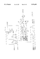
FIGS. 1 and 2 are block diagrams of a computer system incorporating the invention;
FIGS. 3, 4 and 5 are timing diagrams of signals in the computer system of FIG. 2;
FIGS. 6-10 are schematic diagrams of circuitry in the VL-bus/PCI-bus bridge of FIG. 2;
FIGS. B1-B5 are timing diagrams for certain signals on the PCI-bus of FIG. 2.
DETAILED DESCRIPTION
FIG. 1 is a block diagram illustrating pertinent features of a computer system incorporating the invention. The system includes a VL-bus host 102, which may, for example, be an Intel 80386 or 80486 microprocessor, or it may include an Intel Pentium microprocessor in combination with a conventional host-bus/VL-bus bridge. The VL-bus host 102 is connected to a VL-bus 104, comprising VL-bus control lines 106, VL-bus data lines 108, and VL-bus address lines 110. The system can also include a math coprocessor 112 connected to the VL-bus 104; if the VL-bus host includes a bridge, then the math coprocessor 112 can instead be coupled to the host bus (not shown). The system of FIG. 1 also includes a core logic chipset comprising an 82C802G chip 118 and an 82C602 chip 120, both manufactured by OPTi, Inc., Santa Clara, Calif., as well as two sets of buffers 114 and 116. The chipset (referred to collectively herein as 122) is coupled to the VL-bus 104 and provides control and address signals to main memory DRAM 124, cache SRAM 126, as well as other components in the system. The cache SRAM 126 also receives address signals from the VL-bus address lines 110 via buffer 128, and both the cache SRAM 126 and the main memory DRAM 124 are coupled bi-directionally to the VL-bus data lines 108. The system also includes an ISA bus 130, which includes address lines 132, a 16-bit SAID data bus 134, and an 8-bit XD data bus 136. The XD data bus 136, together with accompanying control and address signals (collectively the X-bus), are considered herein to form part of the ISA bus 130.
The core logic chipset 122 is responsible for many functions in the system, including recognizing VL-bus cycles intended for devices which reside on the ISA bus, and translating such cycles onto the ISA bus 130. Address signals are transferred between the VL-bus address leads 110 and the ISA-bus address leads 132 via buffers 116 and the 82C602 data buffer 120, and data is transmitted between the VL-bus data lines 108 and the ISA- bus data lines 134 and 136 via the buffers 114 and the 82C602 data buffer 120. A BIOS ROM and flash EPROM 138 reside on the ISA bus 130, as does a keyboard controller 140 and other ISA-bus peripherals 142. Residing on the VL-bus 104 is a VL-bus device 144, as well as a VL-bus/PCI-bus bridge 146 (also referred to herein as a PCI bridge 146) described in more detail below. The PCI-bus bridge is also described in OPTi, Inc., "82C822 PCIB VESA Local Bus to PCI Bridge Interface," Data Sheet (April, 1994), incorporated herein in its entirety, and is described in Appendix E hereto. The VL-bus/PCI-bus bridge 146 is also connected to a PCI-bus 148, comprising control lines 150 and a multiplexed AD address/data bus 152. A PCI-bus device 154 resides on the PCI-bus 148. Although VL-bus 144 is shown residing exclusively on the VL-bus 104, it will be understood that in accordance with the VL-bus specification incorporated above, such device may also be connected to the ISA bus 130. The signals on the VL-bus 104 and the PCI-bus 148 conform to those set forth above and in the appendices with respect to the respective standards.
FIG. 2 is a block diagram showing some of the components of the system of FIG. 1, and providing additional detail regarding the control signals. Only signals pertinent to an understanding of the invention are illustrated, and it will be understood that other signals exist as well. Referring to FIG. 2, it can be seen that the VL-bus host 102 has its CPU address (CA) lines connected to the VL-bus VA lines 202 and its CD data lines connected to the VL-bus data lines 204. It also has its ADS#, R/W#, M/IO# and D/C# outputs connected to the corresponding VL- bus signal lines 206, 207, 208 and 210. The CLK output of the VL-bus host 102 drives the VL-bus LCLK lines 212, and the VL-bus host 102 BLAST# and BRDY# inputs are connected to receive the signals on the corresponding lines 214 and 216 of the VL-bus. As in conventional VL-bus system implementations, the VL-bus host 102 is not connected to the VL-bus LRDY# signal line 218, but rather has its RDY# input connected the VL-bus RDYRTN# signal line 220. Additionally, although the BOFF# input of the VL-bus host 102 is not used in many conventional VL-bus implementations, in the system of FIGS. 1 and 2, it is connected to a corresponding BOFFB output of the VL-bus/PCI-bus bridge 146 for reasons hereinafter described. The BOFFB output of the VL-bus/PCI bridge 146 is also coupled to a WBACK# input of VL-bus device 144. In Pentium systems, the coupling of BOFFB to WBACK# takes place via an AND gate 223, the other input of which is connected to the HITM# output of the Pentium host.
The VL-bus address lines 202 are also connected to the core logic chipset 122, as are the VL-bus data lines 204, the D/C# line 206, the W/R# line 207, the M/IO# line 208, and the ADS# line 210. The core logic chipset 122 also has its BRDY# and BLAST# lines connected to the respective lines 216 and 214 of the VL-bus 104, has its LRDYI# input connected to the LRDY# line 218 of VL-bus 104, and has its RDY# line connected to the VL-bus RDYRTN# line 220. It also has its HCLK input connected to receive the signal on LCLK line 212. The LDEV# input of core logic chipset 122 is connected as hereinafter described.
As previously mentioned, the VL-bus/PCI-bus bridge 146 has a BOFFB output which is connected to the BOFF# input of the VL-bus host 102. If the host 102 separates the VL-bus 104 from the host bus (not shown) connected to the host CPU, and if such bridge does not translate the BOFF# signal between the two buses, then BOFFB is connected directly to the BOFF# input of the host CPU itself. The VL-bus/PCI-bus bridge 146 also includes an LADSIB signal line connected to the ADS# signal line of the VL-bus 104, an MIOB signal line connected to the M/IO# signal line of VL-bus 104, a DCIB signal line connected to the D/C# signal line of VL-bus 104, VD signal lines connected to the data lines of VL-bus 104, VA signal lines connected to the address lines 202 of VL-bus 104, and a clock input connected to the LCLK line 212 of VL-bus 104. The VL-bus/PCI-bus bridge 146 also includes a BLASTIB signal line connected to the VL-bus BLAST# line, a BRDYIB signal line connected to the BRDY# signal line, an RDYIB input connected to the VL-bus RDYRTN# line 220, and an LRDYOB output connected the VL-bus LRDY# signal line 218.
In a conventional VL-bus system implementation, the VL-bus signal lines LDEV<x># are typically ANDed together before being provided to the VL-bus/ISA-bus core logic chipset 122 LDEV# input. In the present embodiment, however, the combined signal (called LDEVI# is intercepted by the VL-bus/PCI-bus bridge 146 before being provided (by the name LDEVO#) to the LDEV# input of the VL-bus/ISA-bus core logic chipset 122. Accordingly, in FIG. 2, the VL-bus signal lines LDEV0#, LDEV1# and LDEV2# are connected to respective inputs of a 3-input AND gate 222, the output of which forms the LDEVI# signal. This signal is provided to an LDEVIB input of the VL-bus/PCI-bus bridge 146, which produces an LDEVOB output on a signal line LDEVO#. The LDEVO# is connected to the LDEV# input of VL-bus/ISA-bus core logic chipset 122.
On the PCI-bus side of VL-bus/PCI-bus bridge 146, the bridge is connected to the 32-bit multiplexed address/data bus 152. The bridge 146 also has a FRAMEB signal line connected to the FRAME# control signal line of the PCI-bus 148, an IRDYB signal line connected to the IRDY# signal line of the PCI-bus 148, a TRDYB signal line connected to the TRDY# signal line of PCI-bus 148, and a DEVSELIB signal line connected to the DEVSEL# signal line of the PCI-bus 148.
FIG. 2 also illustrates an ISA-bus device 142 connected to the ISA-bus 130 which is connected to the VL-bus/ISA-bus core logic chipset 122, a PCI-bus device 154 which is connected to all of the signal lines of PCI-bus 148, and a VL-bus device 144 which is connected to appropriate signal lines of the VL-bus 104. Pertinent to the present description, the VL-bus device 144 is able to listen to the VL-bus cycle definition signals (VA, BE#, R/W#, D/C#, and M/IO#). If it recognizes a valid cycle to which it can respond, the VL-bus device 144 can assert LDEV# onto the VL-bus LEDVO# signal line, and can terminate its VL-bus cycle by asserting LRDY# on the VL-bus LRDY# signal line 218. The PCI-bus device 154 and the VL-bus device 144 can constitute any desired expansion devices, but typically they will include a video display driver, possibly SCSI adapters, disk controllers, LAN adapters, and so on.
The operation of the system of FIGS. 1 and 2 will be described with respect to certain timing diagrams beginning with FIG. 3. FIG. 3 simplified is a timing diagram illustrating the timing of signals on the VL-bus 104 for a VL-bus read cycle initiated by the VL-bus host 102 and claimed by a conventional VL-line target device. Possible variations, and the timing of various signals not shown in FIG. 3, can be gleaned from the above-incorporated VL-bus specifications. The timing is the same for a VL-bus master-initiated cycle, except that it is preceded by a bus arbitration procedure.
Referring to FIG. 3, the LCLK signal is indicated at line 302. Six LCLK cycles are shown, labeled T1, T21, . . . , T25. Cycle T1 corresponds to the T1 cycle of an Intel 80486 microprocessor, and cycles T21 . . . T25 correspond to five consecutive T2 cycles of such a microprocessor (see the Intel databooks incorporated above).
In LCLK cycle T1, as indicated on line 304, the host 102 places the cycle definition signals (ADR[31:2], M/IO#, W/R#, D/C# and BE[3:0]#) on the appropriate signal lines of the VL-bus 104. It then strobes the ADS# signal to assert the validity of the cycle definition signals and to start the VL-bus cycle as shown in line 306. If a VL-bus target device, such as 144 in FIG. 2, recognizes the cycle definition and desires to claim the VL-bus cycle, it must do so within 20 nanoseconds after sampling ADS# low at the rising edge which begins T21. To claim the cycle, VL-bus target device 144 asserts its LDEV# output onto the VL-bus LDEV<x># signal to which it is connected. This causes AND gate 222 (FIG. 2) to assert LDEVI# low, which signal is passed through the VL-bus/PCI-bus bridge 146 to the LDEVO# signal line and onto the LDEV# input of VL-bus/ISA-bus core logic chipset 122. The core logic chipset 122 samples LDEV# on the first rising edge of LCLK following the 20 nanosecond period to determine whether any VL-bus device has claimed the cycle. Such rising edge is referred to herein as the VL-bus device bus-claiming deadline, and is relative to the LCLK rising edge at which ADS# is sampled asserted. For systems with LCLK≦33.3 MHz, the VL-bus device claiming deadline is typically the first rising edge of LCLK following the rising edge on which ADS# is sampled asserted, and for systems in which LCLK≧40 MHz, the VL-bus device claiming deadline is typically the second rising edge of LCLK following the rising edge in which ADS# is sampled asserted.
Accordingly, referring again to FIG. 3, the VL-bus device 144, through the AND gate 222, asserts LDEVI# within T21 for 33.3 MHz systems (arrow 308), or within T21 or T22 for 40 MHz systems and above (arrow 310), as indicated on line 312. In either case, VL-bus/PCI-bus bridge 146 asserts LDEVO# to the VL-bus/ISA-bus core logic chipset 122 immediately thereafter as indicated on line 314 ( arrows 316 and 318, respectively). (Note that the VL-bus/PCI-bus bridge 146 is at the same time decoding the address and cycle definition signals as described elsewhere herein, and may assert LDEVO# as a result of the decode as well. The bridge 146 therefore may actually assert LDEVO# before receipt of LDEVI# as indicated by arrow 315.)
The VL-bus host 102 unasserts (negates) ADS# 306 after being sampled asserted, i.e. within LCLK cycle T21. The VL-bus device 144 therefore detects ADS# negated at the rising edge which begins T22, and within T22, begins driving its read data onto the VD lines 204 of VL-bus 104 as indicated on line 320.
The cycle definition signals remain active until RDYRTN# is sampled asserted on a rising edge of LCLK, i.e. in LCLK cycle T24 or T25 as indicated by arrows 330 and 331.
After the end of the second T2 state (i.e., in LCLK cycle T23), the VL-bus device 144 begins asserting LRDY# as indicated in line 322 for one LCLK cycle. This signal is detected at the LRDYI# input of the VL-bus/ISA-bus core logic chipset 122, which responds by asserting RDYRTN# on the VL-bus 104 (line 324 and arrow 326 in FIG. 3). For 40 MHz systems and faster, the core logic chipset 122 may wait until the first rising edge of LCLK following detection of LRDY# asserted to assert RDYRTN# (arrow 328), thereby resynchronizing the ready signals with LCLK. For 33 MHz systems, LRDYI# can be connected directly to RDYRTN#. The VL-bus host detects RDYRTN# asserted on its RDY# input, and terminates the VL-bus cycle.
The rising edge of LRDY# in T24 causes the core logic chipset 122 to unassert RDYRTN# either immediately thereafter (arrow 334), or for faster systems, in response to the first LCLK rising edge following detection of LRDY# unasserted (arrow 336). The VL-bus device 144 drives the VL-bus LRDY# signal line to a high logic level for one-half LCLK cycle following deassertion of LRDY#, and then floats LRDY#.
The VL-bus device 144 continues to drive data onto the VD lines 204 until the first LCLK rising edge at which it detects RDYRTN# asserted (arrow 338 or 340). It also cause AND gate 222 to de-assert LDEVI# at the same time (arrows 342, 344), and the VL-bus/PCI-bus bridge 146 de-asserts LDEVO# to the core logic chipset 122 at the same time (arrows 346,348).
Thus it can be seen that the VL-bus/PCI-bus bridge 146 does not interfere with VL-bus read accesses to VL-bus target devices such as 144. The same is true with VL-bus write accesses to VL-bus target devices, and to VL-bus read and write accesses regardless of whether the originator is the VL-bus host 102, the VL-bus/ISA-bus core logic chipset 122 (e.g. acting for an ISA-bus master), or a VL-bus master device. Note that in the timing diagram of FIG. 3, if no VL-bus device had asserted its corresponding LDEV<X># signal by the VL-bus device claiming deadline, then the chipset 122 translates the cycle onto the ISA-bus 130 and returns any read data onto the VD lines 204 of the VL-bus 104.
FIG. 4 is a timing diagram illustrating the operation of the system of FIGS. 1 and 2 when the target device of a VL-bus access resides on the PCI-bus 148. The timing diagram of FIG. 4, like that of FIG. 3, has been simplified for clarity of description. In addition, a system with LCLK≦33.3 MHz is assumed, and it is assumed that the PCI-bus clock is the same as the VL-bus clock, LCLK, but is treated asynchronously.
Referring to FIG. 4, as with FIG. 3, an LCLK signal is indicated on line 402. One T1 cycle is shown, followed by nine T2 cycles labeled T21 . . . , T29. The VL-bus host 102 drives a cycle definition onto the VL-bus 104 prior to T1 as indicated on line 404, and asserts ADS# as indicated on line 406. It is assumed that no VL-bus device claims the cycle, so LDEVI# remains high throughout the VL-bus cycle as indicated on line 408. Nevertheless, the VL-bus/PCI-bus bridge 146 asserts LDEVO# to VL-bus/ISA-bus core logic chipset 122 in response to detection of ADS# asserted at the beginning of the first T2 cycle. The core logic chipset 122 thus considers the VL-bus cycle as having been claimed by a VL-bus device, and withholds any translation of the cycle onto the ISA-bus 130. The VL-bus/PCI-bus bridge 146 also drives the address from VA lines 202 onto the AD lines 152 of PCI-bus 148 (line 412 in FIG. 4), and drives an appropriate command onto the C/BE# lines of PCI-bus 148 (line 414 in FIG. 4). After a delay for synchronizing to the PCI-bus clock signal, in T23, VL-bus/PCI-bus bridge 146 asserts FRAME# on the PCI-bus 148 (line 416 in FIG. 4). It also asserts the PCI-bus IRDY# signal in T24 (line 418). It is assumed that only one data phase will occur on the PCI-bus in response to the present example VL-bus cycle, so the bridge 146 de-asserts FRAME# in T24.
Prior to the PCI-bus device claiming deadline, the target PCI-bus device 154 (FIG. 2) claims the PCI-bus cycle by asserting DEVSEL#. The PCI-bus device 154 is assumed to be a fast device, so as indicated on line 420 (FIG. 4), it asserts DEVSEL# during T24 in response to detection of FRAME# asserted at the rising edge which begins T24. The bridge 146 releases the address and command from the PCI-bus AD and C/BE# signal lines, respectively, in response to the assertion of DEVSEL#, and asserts BE# onto the C/BE# signal lines. In T25, the PCI-bus device 154 drives the read data onto the PCI-bus AD lines 152 and asserts TRDY# for one clock cycle as indicated on line 422. The bridge 146 latches the data from AD lines 152 onto the VL-bus VD data lines 204 as indicated by line 430 and arrow 424 (although initially invalid data may be driven from AD to VD as early as T22). At the beginning of T26, the VL-bus/PCI-bus bridge 146 samples TRDY# asserted, and in response thereto, releases C/BE# and de-asserts IRDY# ( arrows 426 and 428, respectively). The PCI-bus device 154 also releases the AD lines 152 and negates DEVSEL# in T26.
After another synchronization delay, in T28, the VL-bus/PCI-bus bridge 146 asserts LRDY# as indicated on line 432 for one LCLK cycle. The VL-bus/ISA-bus core logic chipset 122 responds by asserting RDYRTN# on the VL-bus 104 (line 434 and arrow 436 in FIG. 4); it de-asserts RDYRTN# in response to the de-assertion of LRDY# (arrow 438). The VL-bus/PCI-bus bridge 146 samples RDYRTN# asserted at the beginning of T29, and in response thereto, negates LDEVO# to the core logic chipset 122 (arrow 440).
Accordingly, it can be seen that the VL-bus/PCI-bus bridge translates VL-bus cycles onto the PCI-bus 148 for response by PCI-bus devices. This is accomplished without the need for any special signals between the VL-bus/PCI-bus bridge 146 and either the VL-bus host 102 or the VL-bus/ISA-bus core logic chipset 122. It will be understood that the same is true of VL-bus data write cycles, and VL-bus cycles originated by VL-bus device masters and by the core logic chipset 122 for an ISA-bus master. Essentially the VL-bus/PCI-bus bridge appears to each of the VL-bus devices as a VL-bus target and appears to each PCI-bus device as the host-bus/PCI-bus bridge. It will also be understood that numerous types of PCI-bus transactions are defined in the PCI-bus specification incorporated above, and while only one such transaction type is illustrated in FIG. 4, different situations may result in different PCI-bus transaction types as appropriate or desirable.
FIG. 5 is a timing diagram illustrating the operation of the system of FIGS. 1 and 2 for a VL-bus read access to a device which resides on the ISA-bus 130 (or to an address to which no device responds). As with FIGS. 3 and 4, the timing diagram of FIG. 5 is simplified for clarity of illustration. Possible variations, and the timing of various signals not shown in FIG. 5, can be gleaned from the above-incorporated references. As with FIGS. 3 and 4, the timing shown in FIG. 5 is the same for a VL-bus master-initiated cycle, except that it is preceded by a bus arbitration procedure.
Referring to FIG. 5, the LCLK signal is illustrated as line 502. Certain signals, such as the VL-bus signals VD and LDEVI#, and PCI-bus signals AD, C/BE#, TRDY#, are omitted from FIG. 5 for clarity. Signal line 504 illustrates the cycle definition signals on the VL-bus 104, and line 506 illustrates the ADS# signal. The VL-bus host 102 drives the cycle definition lines and asserts ADS# during the T1 cycle in order to define a valid VL-bus cycle. At the beginning of T21, the VL-bus/PCI-bus bridge 146 samples ADS# asserted, and asserts LDEVO# in response thereto (line 508 and arrow 540). It is assumed that no other VL-bus device intends to claim the VL-bus cycle, so LDEVI# (not shown in FIG. 5) remains high for the entire process of FIG. 5.
As with the VL-bus cycle illustrated in FIG. 4, after a synchronization delay, the VL-bus/PCI-bus bridge 146 asserts FRAME# during T23 on the PCI-bus 148 as shown at line 510 in FIG. 5. Again, since only one PCI-bus data phase is assumed to be desired, the bridge 146 negates FRAME# during T24. The bridge 146 also asserts IRDY# on the PCI-bus 148 during T24 as indicated at line 512 in FIG. 5.
According to the PCI-bus specification, a PCI-bus controller can be programmed to expect a PCI-bus device claiming signal asserted prior to a PCI-bus claiming deadline which is programmable to be 1, 2 or 3 PCI-clock rising edges after the rising edge at which FRAME# is sampled asserted. This is true of the bridge 146, and it is assumed that the bridge 146 has been programmed for the medium PCI-bus device claiming deadline of two PCI-bus clock cycles. Such programming was accomplished during system boot-up, in which the boot-up code surveyed the PCI-bus devices included in the system and determined that none required longer than two PCI-bus clock cycles to claim a PCI-bus cycle; this information was written into the register address offset 52h(1:0) of the PCI-bus bridge 146. Accordingly, since no PCI-bus device claims the cycle by asserting DEVSEL# by the LCLK rising edge which begins T26, (line 514 in FIG. 5), the VL-bus/PCI-bus bridge 146 issues a "master abort". This negates RDY# (arrow 516).
At this point, since the VL-bus/PCI-bus bridge 146 has asserted LDEVO# to the VL-bus/ISA-bus core logic chipset 122, the chipset 122 will not know that it needs to try finding the destination device on the ISA-bus 130. One solution would be to provide additional signals between the VL-bus/PCI-bus bridge 146 and the core logic chipset 122 in order to so inform the chipset 122, but this would require a modification of standard VL-bus/ISA-bus core logic chipsets such as 122. Accordingly, in the system of FIGS. 1 and 2, the VL-bus/PCI-bus bridge 146, in response to its failure to detect DEVSEL# asserted at the LCLK rising edge which begins T26, asserts BOFF# in T27 to the VL-bus host 102 (line 518 and arrow 520 in FIG. 5). As indicated on line 522 and arrow 524, after assertion of BOFF#, the VL-bus/PCI-bus bridge 146 asserts LRDY# in LCLK cycle T28 to cause the termination of the VL-bus cycle. LRDY# is delayed by one LCLK cycle (programmable to 0, 1 or 2 LCLK cycles) after BOFF# for reasons which will become apparent. As indicated by arrow 528, the VL-bus controller in 122 asserts RDYRTN# in response to detection of LRDY# asserted, and negates RDYRTN# in T29 in response to the negation of LRDY# in T29 (arrow 530). After the PCI-bus bridge 146 detects RDYRTN# asserted at the beginning of LCLK period T29, it negates LDEV# in LCLK period T29 as indicted by arrow 534. It also negates BOFF# in LCLK period T210 as indicated by arrow 532. The delay from RDYRTN# to negation of BOFF#, like the delay from BOFF# to LRDY#, is programmable in PCI-bus bridge 146 in order to be assured that the host CPU has itself received the BOFF# signal despite any time delays in a host-bus/VL-bus bridge in VL-bus host 102.
At the first LCLK rising edge in which BOFF# is sampled negated, the VL-bus host 102 repeats the VL-bus cycle which was aborted by the PCI-bus bridge 146. It does this by starting a new T1 cycle in which it once again drives the cycle definition signals on the VL-bus 104 as indicated on line 504 in FIG. 5, and asserts ADS# as indicated on line 506 in FIG. 5 ( arrows 536 and 538, respectively). The VL-bus host 102 negates ADS# in the following LCLK cycle and withdraws the cycle definition signals in due course. Unlike the initial assertion of the VL-bus cycle, however, the VL-bus/PCI-bus bridge 146 does not assert LDEVO# in response to the repetition of the cycle, nor does it assert any signals on the PCI-bus 148. Instead, the VL-bus/ISA-bus core logic chipset 122 performs its usual duties of translating the cycle to the ISA-bus 130 and returning any read data back to the VL-bus VD lines 204. If no ISA-bus device responds to the access, then as in a conventional system, the data which the chipset 122 returns to the VL-bus VD lines 204 will be undefined. The chipset 122 then assert RDYRTN# for one LCLK cycle to end the VL-bus cycle.
The timing relationship between the PCI-bus bridge's assertion of LRDY# and BOFF# (lines 522 and 518 in FIG. 5) solves a problem which could otherwise preclude the use of LDEVO# and BOFF# to add PCI-bus 148 to a conventional system without modifying the core logic chipset 122. In particular, if the PCI-bus bridge 146 were to assert BOFF# without asserting LRDY#, then the VL-bus controller in VL-bus/PCI-bus core logic chipset 122 would not know one VL-bus cycle has ended and a new VL-bus cycle will soon begin, since the chipset 122 does not necessarily receive BOFF#. Other VL-bus devices would have the same problem, since they too do not necessarily receive BOFF#. VL-bus devices need only observe the RDYRTN# line (and BRDY# with BLAST#) to determine that a VL-bus cycle has ended, and RDYRTN# will not occur unless LRDY# is asserted first. On the other hand, the PCI-bus bridge 146 cannot assert LRDY# without asserting BOFF#, since LRDY# causes the VL-bus controller in core logic chipset 122 to assert RDYRTN#, which is connected to the VL-bus host 102 RDY# input. Thus the VL-bus host 102 would consider the VL-bus cycle terminated successfully, and would have no reason to repeat it. Thus the PCI-bus bridge 146 needs to assert both BOFF# and LRDY#.
If the bridge 146 were to assert LRDY# before asserting BOFF#, then once again, the VL-bus controller in chipset 122 would assert RDYRTN# and the VL-bus host 102 would receive RDY# possibly before it receives BOFF#. In this case the VL-bus host 102 would consider the original VL-bus cycle terminated successfully, begin a subsequent (non-repeat) VL-bus cycle, and apply the back-off to the subsequent cycle instead of the original cycle. On the other hand, if the PCI-bus bridge 146 asserts LRDY# too late, such that the core logic chipset 122 does not assert RDYRTN# until after BOFF# has been negated at the input of the host, then the VL-bus host 102 might repeat the back-offed VL-bus cycle before the VL-bus devices, including that in the VL-bus/ISA-bus core logic chipset 122, can reset their VL-bus state machines and prepare to detect it.
According to an aspect of the invention, therefore, the PCI-bus bridge 146 does not assert LRDY# until after it has asserted BOFF#. The 80486 and Pentium-compatible processors ignore their RDY# input while BOFF# is being asserted. Advantageously, the PCI-bus bridge 146 delays assertion of LRDY# by a number of LCLK cycles in order to ensure that the microprocessor itself has had an opportunity to sample BOFF# asserted before (or no later than the LCLK rising edge that) it detects an active RDY# from the RDYRTN# line. This delay, which is programmable in the PCI-bus bridge 146, accommodates any timing delays which might occur between the BOFFB output of PCI-bus bridge 146 and the BOFF# input of the microprocessor itself. Additionally, the PCI-bus bridge 146 does not negate BOFF# until after it detects RDYRTN# asserted. As previously mentioned, advantageously the PCI-bus bridge 146 can be programmed to delay negation of BOFF# by one or two additional LCLK cycles in order to ensure that BOFF# is still asserted at the host microprocessor BOFF# input when the microprocessor's RDY# input is asserted.
The timing diagram of FIG. 5 also describes a VL-bus master-initiated access to an ISA-bus device. VL-bus devices are not required to receive BOFF#, but they do receive a WBACK# signal. In a conventional system, WBACK# is typically connected to the HITM# output of a Pentium-based VL-bus host. The Pentium contains an on-chip write-back cache memory, and it asserts HITM# whenever it has an internal cache miss and a write-back to system memory is required. When a bus master detects HITM# asserted (e.g. via a WBACK# input), the bus master is required to immediately abort its cycle and float all address data and control signals that it drives as master. When the device later samples WBACK# inactive, the device may restart the bus cycle with a new ADS#.
Conveniently, this required operation of a VL-bus master in response to WBACK# is the same as the operation of the VL-bus host in response to BOFF#. Thus VL-bus masters can be accommodated in a system incorporating the invention, by coupling the BOFFB output of the PCI-bus bridge 146 to the WBACK# inputs of each such device. In systems having a write-back cache, the BOFFB signal can be ANDed with HITM# such that either HITM# or BOFFB will force the VL-bus master to perform a backoff function.
As previously mentioned, some VL-bus implementations are built around a host microprocessor whose data path is twice as wide as the VD lines 204 on VL-bus 104. Such is the case for systems built around the Intel Pentium microprocessor, for example. In order to accommodate these arrangements, a conventional VL-bus system includes a host-bus/VL-bus bridge (not shown) within the VL-bus host 102 of FIG. 2. Such a bridge will assert two accesses on the VL-bus in response to each access on the host bus if the data path on the host bus is twice as wide as that on the VL-bus 104. Described more generally, since it is also possible that a future system could be built around a microprocessor whose data path is four times as wide as the VD lines 204, or more, such bridge will assert a "plurality" of accesses on the VL-bus 104 in response to each access on the host bus (not shown).
In order to accommodate a situation where the host-bus data path is twice as wide as the VL-bus data path, the VL-bus/PCI-bus bridge 146 uses its BE4# input pin to determine whether two VL-bus "sub-cycles" are being issued for each host-bus cycle. In systems whose CPUs have only a 32-bit wide data bus, such as 486 systems, the BE4# input pin is strapped high. In Pentium systems, the BE4# input of the bridge 146 is connected to the BE4# address lead of VL-bus 104. If BE4# is high in a particular cycle, then only one sub-cycle will occur. If BE4# is low in the particular cycle, then two sub-cycles will occur. In the latter case the VL-bus/PCI-bus bridge 146 will assert LDEVO# and subsequently LRDY# for both of the sub-cycles, but will assert BOFF# only for the last such sub-cycle. On repetition, the VL-bus/PCI-bus bridge 146 blocks assertion of LDEVO# for both sub-cycles of the host bus cycle repetition. In this manner, the host-bus/VL-bus bridge (not shown) also need not be modified in any way to accommodate the addition of a VL-bus/PCI-bus bridge such as 146.
In the computer system illustrated in FIGS. 1 and 2, any ISA-bus device, PCI-bus device or VL-bus device, in addition to the VL-bus host 102, can be a master for any particular access. The target for such accesses can be main memory (not shown in FIG. 2), or any ISA-bus device, PCI-bus device, or VL-bus device. The VL-bus/PCI-bus bridge therefore accommodates a wide variety of different kinds of accesses, only some of which have been described in detail with respect to FIGS. 3, 4 and 5. Such descriptions are sufficient for an understanding of the invention, but for completeness, an overview of the remainder of the cycle permutations is included in Appendix E.
FIGS. 6 through 10 are schematic diagrams of pertinent portions of the VL-bus/PCI-bus bridge 146 which control various signals used for implementing the invention. While the descriptions above and in the appendices are sufficient to enable implementation of the invention, descriptions at the schematic level for some aspects are provided for those interested in more details about an example implementation.
FIG. 6 is a schematic diagram for circuitry which generates the LDEVOB output of the PCI-bus bridge 146. It comprises a 3-input NOR gate 602 which generates such a signal, the three inputs of which receive a QN output of a D-flip-flop 604, a DRDEVLO signal, and an LDEVI signal. The LDEVI signal is the inverse of the LDEVIB input of PCI-bus bridge 146. The DRDEVLO signal is generated by a 5-input NOR gate 606, the five inputs of which receive signals labeled: SAMPLEB, H2PENB, BLOCK, ISADEV and HMEMCYC. The SAMPLEB signal is generated by gates 608 in response to WS, T21B and T22B signals according to the formula:
SAMPLEB=(WS+T21B)·T22B.
WS is a programmable signal which is asserted high to indicate that the LCLK signal is operating at a high enough frequency such that the local device claiming deadline is to be delayed by one wait state. T21B is a signal generated by means not shown in the PCI-bus bridge 146, which is asserted low at the beginning of T21 (see FIG. 3, for example) and returns high at the beginning of T22. The T22B signal is asserted low by means not shown in the PCI-bus bridge 146 at the beginning of T22, and returns high at the beginning of T23.
The H2PENB signal is generated by logic 610 in response to the following signals from the VL-bus 104 (FIG. 2): WR, MIO, and DC. The formula to produce H2PENB is:
H2PENB=WR·MIO·DC+MIO·DC.
The BLOCK signal is generated by circuitry described below with respect to FIG. 10, and the ISADEV signal is generated by circuitry (not shown) which, based on a positive decode of the cycle definition signals on VL-bus 104 asserts ISADEV when the intended recipient of the bus cycle is known to reside on the ISA-bus 130 (FIG. 2). The HMEMCYC signal is generated by NOR gate 612, the two inputs of which receive an HMEMB signal and an ENLDEVO signal, respectively. The HMEMB signal corresponds to the LMEM# input of the PCI-bus bridge 146 (see Appendix E) or, depending on a register bit selection, a positive decode of the VL-bus cycle definition signals. If the PCI-bus bridge 146 is programmed to perform such a positive decode, then circuitry (not shown) in PCI-bus bridge 146 asserts HMEMB low when the destination of the cycle is known to be host memory on the host memory bus or VL-bus 104. ENLDEVO is a register bit which is programmable to enable (when asserted high) or disable (when low) the use of HMEMB in the determination of whether to assert LDEVOB.
The flip-flop 604 has a clock input connected to receive CLK, which is the LCLK signal on VL-bus 104. The flip-flop 604 also has a D input connected to receive the output of logic 614, which generates the D input according to the formula:
D=[DRDEVLO+(Q·RST)]·RDYB.
In this formula, Q is the Q output of flip-flop 604, RST is a chip-wide reset signal, and DRDEVLO is a signal generated by NOR gate 606 discussed above. RDYB is generated by logic circuitry 616 according to the inverse of the formula:
RDY=BRDYI·BLASTI+RDYI+BOFFRDY+Other,
where BRDYI and BLASTI are the VL-bus BRDY# and BLAST# signals, respectively; RDYI is connected to the VL-bus RDYRTN# signal line; and "Other" represents other ready signals not important for an understanding of the present invention. BOFFRDY is given by the formula:
BOFFRDY=(FBOLRDY+BOFFP)·BOFFEN,
where FBOLRDY and BOFFP are both generated by circuitry described below with respect to FIGS. 9 and 7, respectively, and BOFFEN is a register bit which enables the entire back-off process when set.
In operation, the circuitry of FIG. 6 asserts LDEVOB low in response to a logic high value on any of the three inputs of NOR gate 602. Thus due to the LDEVI input, it can be seen that whenever any VL-bus device asserts one of the LDEV<x># signal lines in FIG. 2, the LDEVI# signal provided to the PCI-bus bridge 146 will pass therethrough to the LDEV# input of the VL-bus/ISA-bus core logic chipset 122. The other circuitry in FIG. 6 also will activate LDEVOB in most cases, so LDEVOB will remain asserted until the VL-bus device unasserts LDEV<x># or until the flip-flop 604 QN output goes low, whichever occurs later.
The remainder of the circuitry of FIG. 6 operates by asserting DRDEVLO before the VL-bus device claiming deadline, to thereby assert LDEVOB, and by maintaining LDEVOB asserted with the flip-flop 604 until an appropriate ready signal has been received by the PCI-bus bridge 146. More specifically, NOR gate 606 will assert DRDEVLO only when all five of its inputs are low. The SAMPLEB signal is a temporal qualifier on the assertion of DRDEVLO, since SAMPLEB is asserted low only during T22 (for systems with LCLK operating at frequencies greater than or equal to 40 MHz) or during T21 and T22 (for systems operating at LCLK frequencies less than or equal to 33 MHz). The inverse of SAMPLEB is given by:
SAMPLE=(WS·T21)+T22
Thus if NOR gate 606 asserts DRDEVLO at all, it unasserts DRDEVLO at the beginning of T23.
The H2PENB input of NOR gate 606 is asserted low unless the cycle definition signals on VL-bus 104 indicate that the present cycle is an interrupt acknowledge cycle, a halt/special cycle, or a reserved cycle, all as defined at page 7 of the above-incorporated "i486 MICROPROCESSOR" Databook. These are VL-bus cycles which are known in advance not to be destined for any device residing on the PCI-bus bridge 148.
The BLOCK signal input of NOR gate 606 will block assertion of DRDEVLO only if the current VL-bus cycle definition is a repeat of a prior VL-bus cycle for which the PCI-bus bridge 146 asserted BOFF# to the VL-bus host 102. In Pentium-based systems, BLOCK remains asserted for the repetition of both sub-cycles in a repeat of a BOFF#'d host cycle. The BLOCK signal therefore prevents the PCI-bus bridge 146 from claiming the repetition of a VL-bus cycle which the PCI-bus bridge 146 has already attempted on the PCI-bus 148. The circuitry which generates BLOCK is described below with respect to FIG. 10.
The ISADEV signal of NOR gate 606 is asserted high on a positive decode indicating that the target of the current VL-bus cycle is already known to reside on the ISA-bus 130. The ISADEV signal thus prevents the PCI-bus bridge 146 from claiming the cycle and trying it on the PCI-bus first. Note that another embodiment of the invention need not prevent this attempt, but rather can rely on the BOFF# procedures described herein for the cycle eventually to reach the ISA-bus 130.
The HMEMCYC signal is asserted high on a positive decode of the VL-bus cycle, performed either inside or outside the PCI-bus bridge chip 146, to indicate that the access is to host memory. The positive decode, if performed internally to the PCI-bus bridge 146, is performed identically, with a parallel set of configuration registers, to that in the VL-bus/ISA-bus core logic chipset 122. The PCI-bus bridge 146 further includes a register bit ENLDEVO which can be used to permit NOR gate 606 to assert DRDEVLO even if the positive decode indicates that the VL-bus cycle destination is in fact host memory; an attempt by the PCI-bus bridge 146 to claim such a cycle by asserting LDEVO# would not have any effect in most systems because most VL-bus/ISA-bus core logic chipsets ignore their LDEV# inputs when their own internal decode indicates that the VL-bus cycle is to host memory.
Thus it can be seen that the circuitry of FIG. 6 will assert LDEVOB in either the T21 or T22 states of the VL-bus host 102, whichever is appropriate, unless the current VL-bus cycle is a repeat of a prior VL-bus cycle which was subject to BOFF#, and unless it is known in advance that the target of the VL-bus cycle is not on the PCI-bus 148. The latter condition, which may be omitted in whole or in part in a different embodiment, occurs in the present embodiment when it is known in advance that the cycle is a special kind of cycle defined only for targets which do not reside on the PCI-bus, if at all (H2PENB), when the target is known in advance to reside on the ISA-bus 130 (ISADEV), and when the VL-bus cycle is known in advance to be destined for host memory.
When DRDEVLO is asserted, its inverse is written into D-flip-flop 604 on the next LCLK rising edge in order to maintain a logic 1 input of NOR gate 602 from the QN output of flip-flop 604. The logic 614 repeatedly rewrites this value into flip-flop 604 until either a system-wide reset occurs, or RDYB is asserted low by circuitry 616. Circuitry 616 asserts RDYB low upon receipt of RDYRTN# asserted by the VL-bus controller 122. It asserts RDYB low also when it detects both BRDY# and BLAST# asserted on VL-bus 104. Thus the circuitry of FIG. 6 maintains LDEVOB asserted until the rising edge of LCLK which follows completion of the VL-bus cycle which the circuitry claimed by asserting LDEVOB. Note that as described in more detail below, if the PCI-bus bridge 146 did translate the cycle onto the PCI-bus bridge 148, then the RDYRTN# signal will be asserted by the VL-bus controller 122 only after having detected LRDY# asserted by the PCI-bus bridge 146. If the circuitry of FIG. 6 had asserted LDEVOB only because another VL-bus device had caused the assertion of LDEVI, then the cycle will have been terminated only in response to ready signals from the VL-bus device which had claimed the cycle.
The logic circuitry 616 asserts RDYB also in response to a pulse on FBOLRDY or BOFFP, but only if the PCI-bus bridge 146 has been programmed to defeat the back-off feature (BOFFEN=0). FBOLRDY and BOFFP each carry a high-going pulse for one LCLK cycle in response to a master-abort on the PCI-bus 148, although the FBOLRDY pulse occurs only if the current VL-bus cycle is the first sub-cycle of a Pentium cycle, and the BOFFP pulse occurs only if the current VL-bus cycle is anything other than the first sub-cycle of a Pentium cycle. These pulses occur only after the PCI-bus bridge 146 has translated a cycle onto the PCI-bus 148, and failed to detect a PCI-bus device claiming signal prior to the PCI-bus device claiming deadline. Accordingly, if the back-off feature of PCI-bus bridge 146 has been disabled, the logic circuitry 616 causes the release of LDEVO# if the PCI-bus bridge 146 attempted, but failed, to find a target device on the PCI-bus 148. In this case, with BOFFEN=0, it is then up to external circuitry (not shown) to handle the VL-bus cycle.
FIG. 7 is a schematic diagram of circuitry in the PCI-bus bridge 146 which generates the BOFFP signal used in the circuitry of FIG. 6. FIG. 7 also shows circuitry which generates an LBOLRDY signal, and this will be described subsequently. Referring to FIG. 7, the BOFFP signal is the output of a NOR gate 702, one input of which is connected to the Q output of a D-flip-flop 704, the D input of which is connected to the Q output of a flip-flop 706 via an inverter 708. The second input of NOR gate 702 is connected to the Q output of flip-flop 706. Both flip- flops 704 and 706 are clocked by the CLK signal which is connected to the VL-bus LCLK line.
The D input to flip-flop 706 connected to the output of a 4-input NAND gate 710, the inputs of which are connected to signals labeled RSTB, TNH, LASTDW and SMSABORT. The RSTB signal is the system-wide reset signal as previously described. TNH indicates the state of the state machine in PCI-bus bridge 146 which controls PCI-bus cycles. While the details of this state machine are unimportant for an understanding of the present invention, it will be useful to understand that the state machine is in state TNH (TNH=1) while the PCI-bus bridge is controlling a PCI-bus cycle, and is in a TH state (TH=1) while a VL-bus cycle is in process but the PCI-bus bridge 146 will not translate it onto the PCI-bus. The LASTDW signal is generated by circuitry described below with respect to FIG. 8, and basically is asserted during all VL-bus cycles in non-Pentium-based systems, and only during the last data word sub-cycle in Pentium-based systems. Thus LASTDW indicates that the present VL-bus cycle is the last (or only) sub-cycle of a 32-bit or 64-bit access. The SMSABORT signal is generated by circuitry described below with respect to FIG. 9. Essentially it is a PCI-bus master-abort signal, synchronized to the VL-bus LCLK if necessary.
The flip- flop 704 and 706, together with the inverter 708 and NOR gate 702, produce a high-going pulse on the BOFFP in response to a high-to-low transition on the output of NAND gate 710. The output of NAND gate 710 will go low only when all of its inputs are high. Thus it can be seen that the circuitry in FIG. 7 will generate a high-going BOFFP pulse, for one LCLK cycle, in response to a master-abort which occurs while the PCI-bus bridge 146 is translating the last VL-bus cycle of a 32-bit or 64-bit access, onto the PCI-bus 148. As previously mentioned, the circuitry does not generate a pulse on BOFFP if the system is Pentium-based, and the current VL-bus cycle is only the first sub-cycle of a Pentium access. (Note that while reset signals are incorporated throughout the schematic diagrams set forth herein, they are asserted only in unusual situations not relative to an understanding of the present invention. Thus, while their effect can be determined from the schematics, it is unnecessary to describe such effects as well. Hereinafter, reset signals will always be assumed to be unasserted.)
The LASTDW signal is generated by circuitry 802 in FIG. 8 according to the formula:
LASTDW=LBE4+(LHA2·LBE4).
LHA2 is the 22 address bit on the VL-bus 104, and therefore indicates whether the current VL-bus cycle is to an even- or odd-numbered data word address. In non-Pentium-based systems, VL-bus cycles can be addressed to any 32-bit data word. But in Pentium-based systems, a 64-bit access always appears on a 32-bit VL-bus as an access to an even-numbered data word followed by an access to an odd-numbered data word. Thus for Pentium-based systems only, LHA2 indicates which sub-cycle is currently taking place on the VL-bus in response to a 64-bit access.
LBE4 is an input pin which, when asserted, indicates that the system is a Pentium-based system. Thus the circuitry 802 asserts LASTDW whenever the system is not a Pentium-based system (LBE4=1), and if it is a Pentium-based system, asserts LASTDW only during the second sub-cycle of a 64-bit access.
The SMSABORT signal used in the circuitry of FIG. 6 is generated by circuitry 902 in FIG. 9. Circuitry 902 includes an inverting multiplexer 904, the output of which produces SMSABORT. The multiplexer 904 has a `0` input, a `1` input and a select input S, the last of which is connected to receive an ASYNC signal from a register bit. The `0` input of multiplexer 904 is connected to the output of a NAND gate 906, the three inputs of which are connected to receive TNH, MSABORT and an ATSPACE signal. The TNH signal has been described previously, and the MSABORT signal is generated by the PCI-bus bridge 146 in response to the failure of any PCI-bus device to claim a cycle on the PCI-bus 148 prior to the PCI-bus device claiming deadline. The ATSPACE signal is produced by circuitry 908 according to the formula:
ATSPACE=(LMTQ·LT64 K)+(LMIO·ATMEM),
where LMIO is a latched version of the VL-bus M/IO# signal. ATSPACE is asserted for VL-bus I/O cycles to an address within the 64 k I/O memory space, and for VL-bus memory cycles to an address within the 16-megabyte memory address space which can be supported on a standard ISA bus. (In an EISA implementation, the 16-megabyte limitation would be omitted since the EISA-bus supports a full 4 GB of memory address space.) Thus ATSPACE is high for accesses which could possibly be directed to devices residing on the ISA-bus 130; more intuitively, if ATSPACE is low, then the current VL-bus cycle cannot be directed to a device on the ISA-bus 130.
The output of NAND gate 906, in addition to being connected to the `0` input of multiplexer 904, is also connected to one input of a 2-input NAND gate 910, the other input of which is connected to the output of a 3-input NAND gate 912. The output of NAND gate 910 is cross-coupled to one of the inputs of NAND gate 912. The other two inputs of NAND gate 912 are connected to receive RSTB and a ready signal RDYB previously described with respect to FIG. 6. The output of NAND gate 912 is connected to the D input of a flip-flop 914 which is also clocked by LCLK. The output of flip-flop 914 is connected to the `1` input of multiplexer 904.
The circuitry 902 operates in either a synchronous mode or an asynchronous mode, depending on the programming of register bit ASYNC. Basically, if the clock signal on the VL-bus and the PCI-bus are the same, then ASYNC=0 and multiplexer 904 selects the output of NAND gate 906 directly for driving the SMSABORT signal. If the two clocks are asynchronous, either because they operate at different speeds or because clock skew considerations suggest that re-synchronization be performed, the VL-bus host 102 will have programmed ASYNC=1. In this situation, multiplexer 904 selects the LCLK-synchronized output of flip-flop 914 to drive SMSABORT. Essentially cross-coupled NAND gates 910 and 912 latch the signal output of NAND gate 906, and flip-flop 914 synchronizes the result with the VL-bus LCLK signal. The latch is cleared when circuitry 616 (FIG. 6) asserts RDYB, indicating either completion of the VL-bus cycle or, if the back-off feature of PCI-bus bridge 146 is disabled, an appropriate time to clear SMSABORT.
Thus circuitry 902 asserts SMSABORT whenever the output of NAND gate 906 goes low. This occurs only when all three inputs of NAND gate 906 are high, thereby requiring (1) that a master abort have occurred on the PCI-bus 148 (MSABORT=1); (2) that the VL-bus cycle not be to a memory or I/O address which clearly cannot reside on the ISA- bus 130 (ATSPACE=1); and (3) that the PCI-bus bridge 146 presently be translating a cycle onto the PCI-bus 148 (TNH=1) (i.e. SMSABORT will not be asserted if the bridge 146 is not acting as the PCI-bus master).
The FBOLRDY signal, the inverse of which is used in FIG. 6, is generated by circuitry 916 in FIG. 9. Circuitry 916 includes a pulse generator comprising D flip- flops 918 and 920 separated by inverter 922, and 4-input NOR gate 924. The QN outputs of flip- flops 918 and 920 are connected to respective inputs of NOR gate 924, the other two inputs of which are connected to receive LASTDW (previously described) and the inverse of TNH (previously described). It can be seen that if LASTDW=0 and TNH=1, then circuitry 916 will produce a high-going pulse for one LCLK period on FBOLRDY, in response to a high-to-low transition of SMSABORT. The high-going pulse on FBOLRDY will be prevented if TNH=0, indicating that any PCI-bus cycle which resulted in a master-abort was not generated by PCI-bus bridge 146. The high-going pulse on FBOLRDY will be prevented also if LASTDW=1, which occurs for all VL-bus cycles except for the first sub-cycle of a 64-bit Pentium access. Thus considering the circumstances under which circuitry 902 generates SMSABORT, circuitry 916 will produce a high-going pulse on FBOLRDY only in response to a master-abort on the PCI-bus 148, occurring during a PCI-bus cycle originated by PCI-bus bridge 146 (TNH=1) in response a VL-bus cycle which constitutes the first sub-cycle of a Pentium-based 64-bit access.
Circuitry 804 of FIG. 8 generates the BOFFB signal for driving the BOFF# input of VL-bus host 102. Referring to FIG. 8, BOFFB is produced by a 2-input NAND gate 806, one input of which is connected to receive the register programmable BOFFEN signal previously described. The other input of NAND gate 806 is connected to the Q output of a D-flip-flop 808 clocked by LCLK. The D input of flip-flop 808 is driven by circuitry 810 according to the formula:
D=(TNH·CPURDY·LASTDW·SMSABORT)+(Q·RST.multidot.CPURDY).
All signals in this formula have been previously described except Q and CPURDY. Q is the output of flipflop 808, and CPURDY is the output of circuitry 812 (FIG. 8), comprising sequential D-flip-flops 814 and 816 and 4:1 multiplexer 818. The input to the circuitry 812 is the RDYI signal, which is connected to receive RDYRTN# from the VL-bus controller in 122.
The two select inputs of multiplexer 818 are connected to receive two register bits LRDYDL0 and LRDYDL1. In a system with no bridge between the host CPU and the VL-bus 104, the LRDYDL0 and LRDYDL1 signals (collectively, the LRDYDL signals) would be programmed such that multiplexer 818 passes RDYRTN# directly through to CPURDY. In systems which include a host-bus/VL-bus bridge, the LRDYDL signals can be programmed to have multiplexer 818 pass to CPURDY either the Q output of flip-flop 814 or the Q output of flip-flop 816. These represent versions of RDYRTN# delayed by one and two LCLK cycles, respectively. Thus by proper programming of the LRDYDL register bits, the circuitry 812 asserts CPURDY only after it is certain that the RDYRTN# signal on VL-bus 104 has reached and been detected by the host CPU itself on its RDY# input.
In the operation of circuitry 804, referring to the above formula for the D input of flip-flop 808, the NAND gate 806 will never assert BOFFB unless the back-off feature of PCI-bus bridge 146 is enabled (BOFFEN=1). If it is enabled, then the circuitry will assert BOFFB when the first term of the above formula is true. It will hold BOFFB asserted until both terms of the above-formula are false--usually the second term will be true for the longest period of time. The first term will be true in response to a master-abort on the PCI-bus 148 (SMSABORT=1) which was controlled by the PCI-bus bridge (TNH=1) in response to either the only sub-cycle of a 32-bit access or the last sub-cycle of a Pentium 64-bit access (LASTDW=1). CPURDY must also be negated, but this is always the case at the time of SMSABORT. The circuitry 804 will hold D asserted due to the second term of the above formula, until CPURDY is asserted to indicate that RDYRTN# has already reached the host CPU.
As previously described and as described in more detail with reference to schematics below, the assertion by PCI-bus bridge 146 of LRDY# to terminate the VL-bus cycle in the view VL-bus devices, must reach the host CPU neither before nor after BOFF# in order to ensure that the CPU will ignore it. The VL-bus controller 122 generates the signal (RDYRTN#) which drives the RDY# input of the CPU for one LCLK cycle, in response the PCI-bus bridge's assertion of LRDY#. Thus by maintaining BOFFB asserted until 0, 1 or 2 LCLK cycles (as appropriate) after the PCI-bus bridge 146 detects RDYRTN# asserted, circuitry 804 ensures that the BOFF# input of the host CPU will still be active when the host CPU receives an active RDY#.
The LRDYOB signal output of the PCI-bus bridge 146, which drives the LRDY# line of VL-bus 104, is generated by circuitry 926 in FIG. 9, according to the inverse formula:
LRDYO=(FBOLRDY+LBOLRDY)·BOFFEN+H2PLRDY+Others.
The circuitry 926 will assert LRDYOB in response to any one of several readies. In particular, it will assert LRDYOB when a PCI-bus-bridge-originated PCI-bus cycle terminates normally (H2PLRDYB=0), as well as when any of several other readies are received (collectively called "Others"). If the back-off feature is enabled (BOFFEN=1), then circuitry 926 asserts LRDYOB also in response to a pulse on either FBOLRDY or LBOLRDY. FBOLRDY, as previously explained, carries a pulse in response to SMSABORT only if the current VL-bus cycle, which the PCI-bus bridge 146 attempted on the PCI-bus 148 prior to master-abort, was the first sub-cycle of a Pentium 64-bit access. Like BOFFP, described above, LBOLRDY carries a pulse in response to SMSABORT only if the current VL-bus cycle, which the PCI-bus bridge 146 attempted on the PCI-bus 148 prior to master-abort, was the only sub-cycle of a non-Pentium 32-bit access or the last sub-cycle of a Pentium 64-bit access. LBOLRDY is generated from BOFFP by circuitry 712 in FIG. 7, which merely delays the BOFFP pulse by 0, 1 or 2 LCLK cycles depending the programming of the LRDYDL bits. By delaying LBOLRDY in this manner, the PCI-bus bridge 146 ensures that for VL-bus cycles in which BOFF# is asserted to the host CPU, the RDYRTN# signal will not reach the CPU's RDY# input any earlier than BOFF#.
As can be seen, for non-Pentium systems, PCI-bus bridge 146 will generate both BOFF# and LRDY# when its attempt to find a target device on the PCI-bus 148 fails. In a Pentium-based system, the PCI-bus bridge 146 will assert LRDY# in both such sub-cycles, but will assert BOFF# only in the last sub-cycle of the Pentium 64-bit access.
FIG. 10 illustrates circuitry which produces the BLOCK signal used in FIG. 6 to block DRDEVLO when the VL-bus host 102 repeats a cycle which has been subject to BOFF#. As shown in FIG. 10, BLOCK is produced by 2-input NAND gate 1002, one input of which is connected to receive a BLOCK2B signal, and the other of which is connected to the output of an OR gate 1004. One input of OR gate 1004 is connected to the output of logic 1006, which asserts its output low according to the formula:
S1006=(T21+T22)·SAMECYC.
SAMECYC is a signal generated by circuitry (not shown) in the PCI-bus bridge 146 which indicates that the current VL-bus cycle definition signals match those previously latched for the VL-bus which is subject to the BOFF#. For Pentium-based systems, SAMECYC is asserted on both sub-cycles of a Pentium 64-bit access.
The other input of OR gate 1004 is connected to the QN output of a D-flip-flop 1008, the D input of which is connected the output of circuitry 1010 which drives D according to the formula:
D=BOFF+(Q·RST·UNBLOCK.
UNBLOCK is the QN output of a D flip-flop 1012, the D input of which is connected to the output of a 3-input NOR gate 1014. The three inputs of NOR gate 1014 are connected to receive RSTB, TH and SAMECYC.
The BLOCK2B signal is the Q output of a D flip-flop 1016, the D input of which is connected to the output of logic 1018 implementing the inverse of the formula:
D={[(TH·LBE4·LHA2·BOFFEN·SAMECYC).multidot.BLOCK2]+[(TH+LHA2)·BLOCK2]}·RST.
In operation, NAND gate 1002, in combination with OR gate 1004, asserts BLOCK whenever BLOCK2B goes low and whenever both the output of circuitry 1006 and the QN output of flip-flop 1008 are low. Essentially, the QN output of flip-flop 1008 goes low when BOFFB is asserted, and remains low until flip-flop 1012 asserts UNBLOCK. Flip-flop 1012 asserts UNBLOCK when the cycle repetition appears. Circuitry 1006 temporally qualifies BLOCK by allowing the QN output of flip-flop 1008 to pass through OR gate 1004 only during T21 and T22 of the cycle repetition.
Since flip-flop 1008 is cleared when the cycle repetition appears, its QN output is no longer low during the second sub-cycle of a Pentium-based 64-bit access. In this situation, BLOCK2B is low. Referring to the above formula for the D input of flip-flop 1016, it can be seen from the first term that a logic 0 will be written into the flip-flop on the first sub-cycle (LHA2=0) of the cycle repetition (SAMECYC=1) of a Pentium-based (LBE4=1) host memory cycle (TH=1) in a system where the back-off feature of PCI-bus bridge 146 is enabled (BOFFEN=1). Thereafter, since BLOCK2=1, the second term of the formula will control the writing of a logic 1 into the flip-flop 1016. Specifically, the circuitry 1018 will maintain BLOCK2B=0 until the end of the second (LHA2=1) host memory (TH=1) VL-bus cycle of the Pentium 64-bit access.
Thus the circuitry of FIG. 10 will correctly block assertion by the PCI-bus bridge 146 of LDEVO# for the only sub-cycle of the repetition of a BOFF#'d nonPentium-originated access, and for both sub-cycles of a repetition of a BOFF#'d Pentium 64-bit access.
As used herein, a given signal or event is "responsive" to a predecessor signal or event if the predecessor signal or event influenced the given signal or event. If there is an intervening processing element or time period, the given event or signal can still be "responsive" to the predecessor signal or event. If the intervening processing element combines more than one signal or event, the signal output of the processing element is considered "responsive" to each of the signal or event inputs. If the given signal or event is the same as the predecessor signal or event, this is merely a degenerate case in which the given signal or event is still considered to be "responsive" to the predecessor signal or event.
The foregoing description of preferred embodiments of the present invention has been provided for the purposes of illustration and description. It is not intended to be exhaustive or to limit the invention to the precise forms disclosed. Obviously, many modifications and variations will be apparent to practitioners skilled in this art. For example, adaptations will be apparent for using the invention with an EISA bus instead of an ISA bus. The embodiments described herein were chosen and described in order to best explain the principles of the invention and its practical application, thereby enabling others skilled in the art to understand the invention for various embodiments and with various modifications as are suited to the particular use contemplated. It is intended that the scope of the invention be defined by the following claims and their equivalents. ##SPC1##

Claims (15)

We claim:
1. A method for bridging a first bus cycle to a second bus, in a system including a first bus having first bus cycle definition lines,
said system further including said second bus, said second bus having second bus cycle definition lines,
for use with a first bus master defining said first bus cycle by asserting first bus cycle definition signals on said first bus cycle definition lines, said first bus master further having a back-off input line which causes said first bus master to repeat said first bus cycle after detecting assertion of a back-off signal on said back-off input line,
said method comprising the steps of:
defining a cycle on said second bus in response to a first assertion of said first bus cycle start signal by asserting second bus cycle definition signals on said second bus cycle definition lines; and
asserting said back-off signal in response to a predefined event occurring on said second bus in response to said assertion of second bus cycle definition signals on said second bus cycle definition lines.
2. A method according to claim 1, wherein said predefined event is defined at least in part by expiration of a predefined time period that begins in response to said assertion of second bus cycle definition signals on said second bus cycle definition lines.
3. A method according to claim 2, wherein said predefined event is defined further by non-detection of a predefined signal before expiration of said predefined time period.
4. A method according to claim 1, wherein said predefined event occurs on said second bus without any intervening event occurring on said second bus in response to said assertion of second bus cycle definition signals on said second bus cycle definition lines.
5. A method according to claim 1, wherein said second bus further has a second bus device claiming signal line,
and wherein said predefined event is defined at least in part by non-assertion of a second bus device claiming signal on said second bus device claiming signal line before a predetermined second bus device claiming deadline following said assertion of second bus cycle definition signals on said second bus cycle definition lines.
6. A method according to claim 5, wherein said first bus further has a first bus device claiming signal line, and wherein at the time of said first assertion of said first bus cycle start signal the signals on said first bus cycle definition lines are within a predetermined set of first bus cycle definitions,
for use further with a third bus and a first-bus/third-bus bridge coupled to receive said first bus cycle definition signals, said first-bus/third-bus bridge defining a cycle on said third bus in response to certain combinations of said first bus cycle definition signals only if no first bus device claiming signal is asserted before a predetermined first bus device claiming deadline following detection by said first-bus/third-bus bridge of an asserted first bus cycle start signal,
further comprising the step of asserting said first bus device claiming signal prior to said first bus device claiming deadline, in response to said first assertion of said first bus cycle start signal.
7. A method according to claim 1, wherein the signals on said first bus cycle definition lines at the time of said first assertion of said first bus cycle start signal define a first valid first bus cycle, further comprising the steps of:
after assertion of said back-off signal in said step of asserting said back-off signal, in response to a second assertion of said first bus cycle start signal, determining whether a second valid first bus cycle defined by signals then asserted on said first bus cycle definition lines is a repetition of said first valid first bus cycle; and
defining a cycle on said second bus in response to said second assertion of first bus cycle start signal by asserting second bus cycle definition signals on said second bus cycle definition lines , only if said second valid first bus cycle is not a repetition of said first valid first bus cycle.
8. A method according to claim 1, for use further with a third bus having third bus cycle definition lines, further comprising a step of defining a cycle on said third bus in dependence upon said first bus cycle, after said step of defining a cycle on said second bus.
9. A method according to claim 8, wherein said step of defining a cycle on said third bus occurs after said step of asserting said back-off signal .
10. Apparatus for bridging a first bus cycle to a second bus, in a system including a first bus having first bus cycle definition lines,
said system further including said second bus, said second bus having second bus cycle definition lines,
for use with a first bus master defining said first bus cycle by asserting first bus cycle definition signals on said first bus cycle definition lines, said first bus master further having a back-off input line and repeating said first bus cycle after detecting assertion of a back-off signal on said back-off input line,
comprising:
second bus interface logic which defines a cycle on said second bus in response to a first assertion of said first bus cycle start signal by asserting second bus cycle definition signals on said second bus cycle definition lines; and
first bus interface logic which asserts said backoff signal in response to a predefined event occurring on said second bus in response to said assertion of second bus cycle definition signals on said second bus cycle definition lines.
11. Apparatus according to claim 10, wherein said second bus further has a second bus device claiming signal line,
and wherein said predefined event is defined at least in part by non-assertion of a second bus device claiming signal on said second bus device claiming signal line before a predetermined second bus device claiming deadline following said assertion of second bus cycle definition signals on said second bus cycle definition lines.
12. Apparatus according to claim 11, wherein said first bus further has a first bus device claiming signal line, and wherein at the time of said first assertion of said first bus cycle start signal the signals on said first bus cycle definition lines are within a predetermined set of first bus cycle definitions,
for use further with a third bus and a first-bus/third-bus bridge coupled to receive said first bus cycle definition signals, said first-bus/third-bus bridge defining a cycle on said third bus in response to certain combinations of said first bus cycle definition signals only if no first bus device claiming signal is asserted before a predetermined first bus device claiming deadline following detection by said first-bus/third-bus bridge of an asserted first bus cycle start signal,
further comprising circuitry which asserts said first bus device claiming signal prior to said first bus device claiming deadline, in response to said first assertion of said first bus cycle start signal.
13. Apparatus according to claim 10, wherein the signals on said first bus cycle definition lines at the time of said first assertion of said first bus cycle start signal define a first valid first bus cycle,
further comprising a repetition detector which, after assertion of said back-off signal by said first bus interface logic in response to said predefined event, in response to a second assertion of said first bus cycle start signal, determines whether a second valid first bus cycle defined by signals then asserted on said first bus cycle definition lines is a repetition of said first valid first bus cycle,
and wherein said second bus interface logic further defines a cycle on said second bus in response to said second assertion of first bus cycle start signal by asserting second bus cycle definition signals on said second bus cycle definition lines, only if said repetition detector determines that said second valid first bus cycle is not a repetition of said first valid first bus cycle.
14. Apparatus according to claim 10, for use further with a third bus having third bus cycle definition lines, further comprising third bus interface logic which defines a cycle on said third bus in dependence upon said first bus cycle, after said second bus interface logic defines a cycle on said second bus.
15. Apparatus according to claim 14, wherein said third bus interface logic defines said cycle on said third bus after said first bus interface logic asserts said back-off signal.
US09/087,229 1994-11-01 1998-05-29 Using a back-off signal to bridge a first bus to a second bus Expired - Lifetime US5974495A (en)

Priority Applications (2)

Application Number Priority Date Filing Date Title
US09/087,229 US5974495A (en) 1994-11-01 1998-05-29 Using a back-off signal to bridge a first bus to a second bus
JP15032199A JP2000138917A (en) 1998-05-29 1999-05-28 Security completing system and its method

Applications Claiming Priority (3)

Application Number Priority Date Filing Date Title
US33285894A 1994-11-01 1994-11-01
US08/715,901 US5790831A (en) 1994-11-01 1996-09-18 VL-bus/PCI-bus bridge
US09/087,229 US5974495A (en) 1994-11-01 1998-05-29 Using a back-off signal to bridge a first bus to a second bus

Related Parent Applications (1)

Application Number Title Priority Date Filing Date
US08/715,901 Continuation US5790831A (en) 1994-11-01 1996-09-18 VL-bus/PCI-bus bridge

Publications (1)

Publication Number Publication Date
US5974495A true US5974495A (en) 1999-10-26

Family

ID=23300154

Family Applications (2)

Application Number Title Priority Date Filing Date
US08/715,901 Expired - Lifetime US5790831A (en) 1994-11-01 1996-09-18 VL-bus/PCI-bus bridge
US09/087,229 Expired - Lifetime US5974495A (en) 1994-11-01 1998-05-29 Using a back-off signal to bridge a first bus to a second bus

Family Applications Before (1)

Application Number Title Priority Date Filing Date
US08/715,901 Expired - Lifetime US5790831A (en) 1994-11-01 1996-09-18 VL-bus/PCI-bus bridge

Country Status (1)

Country Link
US (2) US5790831A (en)

Cited By (3)

* Cited by examiner, † Cited by third party
Publication number Priority date Publication date Assignee Title
US6233638B1 (en) * 1998-03-20 2001-05-15 Micron Electronics, Inc. System for configuring peer devices
US6349347B1 (en) 1998-03-20 2002-02-19 Micron Technology, Inc. Method and system for shortening boot-up time based on absence or presence of devices in a computer system
US6778543B1 (en) * 1999-03-12 2004-08-17 Canon Kabushiki Kaisha Method and device for controlling the synchronization between two serial communication buses of a network

Families Citing this family (90)

* Cited by examiner, † Cited by third party
Publication number Priority date Publication date Assignee Title
US5790831A (en) * 1994-11-01 1998-08-04 Opti Inc. VL-bus/PCI-bus bridge
US6081852A (en) * 1996-04-26 2000-06-27 Texas Instruments Incorporated Packet data transferring system for autonomously operating a DMA by autonomous boot mode select signal wherein the DMA is enabled to at least one program control list
US5935223A (en) * 1996-05-21 1999-08-10 Texas Instruments Incorporated System for blocking access to a computer device using a glue logic circuit operable to force a target computer device to perform a target abort
US5935220A (en) * 1996-08-09 1999-08-10 Motorola Inc. Apparatus and method for high speed data and command transfer over an interface
US6189109B1 (en) 1997-05-13 2001-02-13 Micron Electronics, Inc. Method of remote access and control of environmental conditions
US6173346B1 (en) 1997-05-13 2001-01-09 Micron Electronics, Inc. Method for hot swapping a programmable storage adapter using a programmable processor for selectively enabling or disabling power to adapter slot in response to respective request signals
US6272648B1 (en) 1997-05-13 2001-08-07 Micron Electronics, Inc. System for communicating a software-generated pulse waveform between two servers in a network
US6243773B1 (en) 1997-05-13 2001-06-05 Micron Electronics, Inc. Configuration management system for hot adding and hot replacing devices
US6247079B1 (en) 1997-05-13 2001-06-12 Micron Electronics, Inc Apparatus for computer implemented hot-swap and hot-add
US6247080B1 (en) 1997-05-13 2001-06-12 Micron Electronics, Inc. Method for the hot add of devices
US6170028B1 (en) 1997-05-13 2001-01-02 Micron Electronics, Inc. Method for hot swapping a programmable network adapter by using a programmable processor to selectively disabling and enabling power thereto upon receiving respective control signals
US6269417B1 (en) 1997-05-13 2001-07-31 Micron Technology, Inc. Method for determining and displaying the physical slot number of an expansion bus device
US6163849A (en) 1997-05-13 2000-12-19 Micron Electronics, Inc. Method of powering up or powering down a server to a maintenance state
US6247898B1 (en) 1997-05-13 2001-06-19 Micron Electronics, Inc. Computer fan speed control system
US6138250A (en) 1997-05-13 2000-10-24 Micron Electronics, Inc. System for reading system log
US6148355A (en) 1997-05-13 2000-11-14 Micron Electronics, Inc. Configuration management method for hot adding and hot replacing devices
US5962933A (en) * 1997-05-13 1999-10-05 Micron Electronics, Inc. Computer fan speed control method
US6304929B1 (en) 1997-05-13 2001-10-16 Micron Electronics, Inc. Method for hot swapping a programmable adapter by using a programmable processor to selectively disabling and enabling power thereto upon receiving respective control signals
US6192434B1 (en) 1997-05-13 2001-02-20 Micron Electronics, Inc System for hot swapping a programmable adapter by using a programmable processor to selectively disabling and enabling power thereto upon receiving respective control signals
US5987554A (en) 1997-05-13 1999-11-16 Micron Electronics, Inc. Method of controlling the transfer of information across an interface between two buses
US6179486B1 (en) 1997-05-13 2001-01-30 Micron Electronics, Inc. Method for hot add of a mass storage adapter on a system including a dynamically loaded adapter driver
US6134673A (en) 1997-05-13 2000-10-17 Micron Electronics, Inc. Method for clustering software applications
US5892928A (en) 1997-05-13 1999-04-06 Micron Electronics, Inc. Method for the hot add of a network adapter on a system including a dynamically loaded adapter driver
US6499073B1 (en) 1997-05-13 2002-12-24 Micron Electronics, Inc. System using programmable processor for selectively enabling or disabling power to adapter in response to respective request signals
US6195717B1 (en) 1997-05-13 2001-02-27 Micron Electronics, Inc. Method of expanding bus loading capacity
US6202160B1 (en) 1997-05-13 2001-03-13 Micron Electronics, Inc. System for independent powering of a computer system
US5990582A (en) * 1997-05-13 1999-11-23 Micron Electronics, Inc. Computer fan speed control device
US6338150B1 (en) 1997-05-13 2002-01-08 Micron Technology, Inc. Diagnostic and managing distributed processor system
US6249834B1 (en) 1997-05-13 2001-06-19 Micron Technology, Inc. System for expanding PCI bus loading capacity
US6243838B1 (en) 1997-05-13 2001-06-05 Micron Electronics, Inc. Method for automatically reporting a system failure in a server
US6145098A (en) 1997-05-13 2000-11-07 Micron Electronics, Inc. System for displaying system status
US6282673B1 (en) 1997-05-13 2001-08-28 Micron Technology, Inc. Method of recording information system events
US6249885B1 (en) 1997-05-13 2001-06-19 Karl S. Johnson Method for managing environmental conditions of a distributed processor system
US6363497B1 (en) 1997-05-13 2002-03-26 Micron Technology, Inc. System for clustering software applications
US6253334B1 (en) 1997-05-13 2001-06-26 Micron Electronics, Inc. Three bus server architecture with a legacy PCI bus and mirrored I/O PCI buses
US6122746A (en) 1997-05-13 2000-09-19 Micron Electronics, Inc. System for powering up and powering down a server
US6219734B1 (en) 1997-05-13 2001-04-17 Micron Electronics, Inc. Method for the hot add of a mass storage adapter on a system including a statically loaded adapter driver
US6134668A (en) 1997-05-13 2000-10-17 Micron Electronics, Inc. Method of selective independent powering of portion of computer system through remote interface from remote interface power supply
US6170067B1 (en) 1997-05-13 2001-01-02 Micron Technology, Inc. System for automatically reporting a system failure in a server
US6122758A (en) 1997-05-13 2000-09-19 Micron Electronics, Inc. System for mapping environmental resources to memory for program access
US6292905B1 (en) 1997-05-13 2001-09-18 Micron Technology, Inc. Method for providing a fault tolerant network using distributed server processes to remap clustered network resources to other servers during server failure
US6202111B1 (en) 1997-05-13 2001-03-13 Micron Electronics, Inc. Method for the hot add of a network adapter on a system including a statically loaded adapter driver
US6526333B1 (en) 1997-05-13 2003-02-25 Micron Technology, Inc. Computer fan speed control system method
US6330690B1 (en) 1997-05-13 2001-12-11 Micron Electronics, Inc. Method of resetting a server
US6249828B1 (en) 1997-05-13 2001-06-19 Micron Electronics, Inc. Method for the hot swap of a mass storage adapter on a system including a statically loaded adapter driver
US6073255A (en) 1997-05-13 2000-06-06 Micron Electronics, Inc. Method of reading system log
US6324608B1 (en) 1997-05-13 2001-11-27 Micron Electronics Method for hot swapping of network components
US6269412B1 (en) 1997-05-13 2001-07-31 Micron Technology, Inc. Apparatus for recording information system events
US6182180B1 (en) 1997-05-13 2001-01-30 Micron Electronics, Inc. Apparatus for interfacing buses
US5892964A (en) * 1997-06-30 1999-04-06 Compaq Computer Corp. Computer bridge interfaces for accelerated graphics port and peripheral component interconnect devices
US5938777A (en) * 1997-07-31 1999-08-17 Advanced Micro Devices, Inc. Cycle list based bus cycle resolution checking in a bus bridge verification system
US6286072B1 (en) * 1997-08-19 2001-09-04 International Business Machines Corporation System and method for synchronizing data communication between asynchronous buses
US5999743A (en) * 1997-09-09 1999-12-07 Compaq Computer Corporation System and method for dynamically allocating accelerated graphics port memory space
US6032213A (en) * 1997-09-11 2000-02-29 Advanced Micro Devices, Inc. PC core logic chipset comprising a serial register access bus
US6263387B1 (en) 1997-10-01 2001-07-17 Micron Electronics, Inc. System for automatically configuring a server after hot add of a device
US6154835A (en) 1997-10-01 2000-11-28 Micron Electronics, Inc. Method for automatically configuring and formatting a computer system and installing software
US6175490B1 (en) 1997-10-01 2001-01-16 Micron Electronics, Inc. Fault tolerant computer system
US6212585B1 (en) 1997-10-01 2001-04-03 Micron Electronics, Inc. Method of automatically configuring a server after hot add of a device
US6035420A (en) 1997-10-01 2000-03-07 Micron Electronics, Inc. Method of performing an extensive diagnostic test in conjunction with a bios test routine
US6088816A (en) 1997-10-01 2000-07-11 Micron Electronics, Inc. Method of displaying system status
US6009541A (en) 1997-10-01 1999-12-28 Micron Electronics, Inc. Apparatus for performing an extensive diagnostic test in conjunction with a bios test routine
US6065053A (en) 1997-10-01 2000-05-16 Micron Electronics, Inc. System for resetting a server
US6275888B1 (en) * 1997-11-19 2001-08-14 Micron Technology, Inc. Method for configuring peer-to-peer bus bridges in a computer system using shadow configuration registers
US6233531B1 (en) 1997-12-19 2001-05-15 Advanced Micro Devices, Inc. Apparatus and method for monitoring the performance of a microprocessor
US5991833A (en) * 1998-03-13 1999-11-23 Compaq Computer Corporation Computer system with bridge logic that reduces interference to CPU cycles during secondary bus transactions
US6226700B1 (en) * 1998-03-13 2001-05-01 Compaq Computer Corporation Computer system with bridge logic that includes an internal modular expansion bus and a common master interface for internal master devices
US6298409B1 (en) 1998-03-26 2001-10-02 Micron Technology, Inc. System for data and interrupt posting for computer devices
US6421746B1 (en) 1998-03-26 2002-07-16 Micron Electronics, Inc. Method of data and interrupt posting for computer devices
US6223299B1 (en) * 1998-05-04 2001-04-24 International Business Machines Corporation Enhanced error handling for I/O load/store operations to a PCI device via bad parity or zero byte enables
US6240480B1 (en) * 1998-05-07 2001-05-29 Advanced Micro Devices, Inc. Bus bridge that provides selection of optimum timing speed for transactions
US5948090A (en) * 1998-06-05 1999-09-07 Compaq Computer Corporation Method and apparatus for controlling reset of component boards in a computer system
US6163835A (en) * 1998-07-06 2000-12-19 Motorola, Inc. Method and apparatus for transferring data over a processor interface bus
US6205503B1 (en) 1998-07-17 2001-03-20 Mallikarjunan Mahalingam Method for the hot swap and add of input/output platforms and devices
US6223234B1 (en) 1998-07-17 2001-04-24 Micron Electronics, Inc. Apparatus for the hot swap and add of input/output platforms and devices
US6223239B1 (en) * 1998-08-12 2001-04-24 Compaq Computer Corporation Dual purpose apparatus, method and system for accelerated graphics port or system area network interface
US6567414B2 (en) * 1998-10-30 2003-05-20 Intel Corporation Method and apparatus for exiting a deadlock condition
US6336158B1 (en) * 1998-10-30 2002-01-01 Intel Corporation Memory based I/O decode arrangement, and system and method using the same
US6161161A (en) * 1999-01-08 2000-12-12 Cisco Technology, Inc. System and method for coupling a local bus to a peripheral component interconnect (PCI) bus
GB0028353D0 (en) * 2000-11-21 2001-01-03 Aspex Technology Ltd Improvements relating to digital data communications
ITMI20021583A1 (en) * 2002-07-18 2004-01-19 St Microelectronics Srl AUTOMATIC DECODING METHOD FOR MAPPING AND SELECTION OF A NON-VOLATILE MEMORY DEVICE WITH A COMMON SERIAL INTERFACE
US7093153B1 (en) * 2002-10-30 2006-08-15 Advanced Micro Devices, Inc. Method and apparatus for lowering bus clock frequency in a complex integrated data processing system
US7114032B2 (en) * 2003-07-18 2006-09-26 International Business Machines Corporation Method and system for efficient fragment caching
KR100543461B1 (en) * 2003-07-22 2006-01-20 삼성전자주식회사 Flash memory device having variable data output function and memory system including the same
US6956782B2 (en) * 2003-09-30 2005-10-18 Infineon Technologies Ag Selective bank refresh
US7596652B2 (en) * 2004-05-14 2009-09-29 Intel Corporation Integrated circuit having processor and bridging capabilities
DE102004029549A1 (en) * 2004-06-18 2006-01-05 Bosch Rexroth Aktiengesellschaft Bus module
JP4869714B2 (en) * 2006-01-16 2012-02-08 株式会社ソニー・コンピュータエンタテインメント Information processing apparatus, signal transmission method, and bridge
US8122322B2 (en) 2007-07-31 2012-02-21 Seagate Technology Llc System and method of storing reliability data
US7554858B2 (en) * 2007-08-10 2009-06-30 Micron Technology, Inc. System and method for reducing pin-count of memory devices, and memory device testers for same
US9201790B2 (en) * 2007-10-09 2015-12-01 Seagate Technology Llc System and method of matching data rates

Citations (4)

* Cited by examiner, † Cited by third party
Publication number Priority date Publication date Assignee Title
US5448704A (en) * 1994-03-07 1995-09-05 Vlsi Technology, Inc. Method for performing writes of non-contiguous bytes on a PCI bus in a minimum number of write cycles
US5784592A (en) * 1995-09-11 1998-07-21 Advanced Micro Devices, Inc. Computer system which includes a local expansion bus and a dedicated real-time bus for increased multimedia performance
US5790831A (en) * 1994-11-01 1998-08-04 Opti Inc. VL-bus/PCI-bus bridge
US5805905A (en) * 1995-09-06 1998-09-08 Opti Inc. Method and apparatus for arbitrating requests at two or more levels of priority using a single request line

Family Cites Families (6)

* Cited by examiner, † Cited by third party
Publication number Priority date Publication date Assignee Title
IT1230238B (en) * 1989-06-08 1991-10-18 Bull Hn Information Syst VME TO MULTIBUS II INTERFACE ADAPTER.
US5309568A (en) * 1992-03-16 1994-05-03 Opti, Inc. Local bus design
US5379384A (en) * 1992-06-05 1995-01-03 Intel Corporation Configuration data loopback in a bus bridge circuit
US5335326A (en) * 1992-10-01 1994-08-02 Xerox Corporation Multichannel FIFO device channel sequencer
US5455915A (en) * 1993-12-16 1995-10-03 Intel Corporation Computer system with bridge circuitry having input/output multiplexers and third direct unidirectional path for data transfer between buses operating at different rates
US5446869A (en) * 1993-12-30 1995-08-29 International Business Machines Corporation Configuration and RAM/ROM control of PCI extension card residing on MCA adapter card

Patent Citations (4)

* Cited by examiner, † Cited by third party
Publication number Priority date Publication date Assignee Title
US5448704A (en) * 1994-03-07 1995-09-05 Vlsi Technology, Inc. Method for performing writes of non-contiguous bytes on a PCI bus in a minimum number of write cycles
US5790831A (en) * 1994-11-01 1998-08-04 Opti Inc. VL-bus/PCI-bus bridge
US5805905A (en) * 1995-09-06 1998-09-08 Opti Inc. Method and apparatus for arbitrating requests at two or more levels of priority using a single request line
US5784592A (en) * 1995-09-11 1998-07-21 Advanced Micro Devices, Inc. Computer system which includes a local expansion bus and a dedicated real-time bus for increased multimedia performance

Cited By (3)

* Cited by examiner, † Cited by third party
Publication number Priority date Publication date Assignee Title
US6233638B1 (en) * 1998-03-20 2001-05-15 Micron Electronics, Inc. System for configuring peer devices
US6349347B1 (en) 1998-03-20 2002-02-19 Micron Technology, Inc. Method and system for shortening boot-up time based on absence or presence of devices in a computer system
US6778543B1 (en) * 1999-03-12 2004-08-17 Canon Kabushiki Kaisha Method and device for controlling the synchronization between two serial communication buses of a network

Also Published As

Publication number Publication date
US5790831A (en) 1998-08-04

Similar Documents

Publication Publication Date Title
US5974495A (en) Using a back-off signal to bridge a first bus to a second bus
US5802324A (en) Computer system with PCI repeater between primary bus and second bus
US5533204A (en) Split transaction protocol for the peripheral component interconnect bus
US6226700B1 (en) Computer system with bridge logic that includes an internal modular expansion bus and a common master interface for internal master devices
KR100742718B1 (en) Transparent bridges connected between the first and second buses of a computer system, systems comprising the same and methods of bridging the first and second buses of a computer system
US5838932A (en) Transparent PCI to PCI bridge with dynamic memory and I/O map programming
US6070215A (en) Computer system with improved transition to low power operation
US5991833A (en) Computer system with bridge logic that reduces interference to CPU cycles during secondary bus transactions
US5309568A (en) Local bus design
US5774681A (en) Method and apparatus for controlling a response timing of a target ready signal on a PCI bridge
US5918072A (en) System for controlling variable length PCI burst data using a dummy final data phase and adjusting the burst length during transaction
US6101566A (en) Computer system with bridge logic that includes an internal modular expansion bus and a common target interface for internal target devices
US5949981A (en) Deadlock avoidance in a bridge between a split transaction bus and a single envelope bus
EP0591419B1 (en) Method and apparatus for expanding a backplane interconnecting bus without additional byte select signals
US6209053B1 (en) Method and apparatus for operating an adaptive multiplexed address and data bus within a computer system
US5918026A (en) PCI to PCI bridge for transparently completing transactions between agents on opposite sides of the bridge
US5559968A (en) Non-conforming PCI bus master timing compensation circuit
US5867728A (en) Preventing corruption in a multiple processor computer system during a peripheral device configuration cycle
US5890002A (en) System and method for bus master emulation
US5832243A (en) Computer system implementing a stop clock acknowledge special cycle
US5590316A (en) Clock doubler and smooth transfer circuit
US6076128A (en) Data transfer method between buses, bridge devices for interconnecting buses, and data processing system including multiple buses
WO2004064286A2 (en) Flow-through register
US5809260A (en) Burst mode data transmission retry of previously aborted block transfer of data
US5878239A (en) Method and apparatus for processing a target retry from a PCI target device to an ISA master devise using a PCI/ISA bridge

Legal Events

Date Code Title Description
STCF Information on status: patent grant

Free format text: PATENTED CASE

FEPP Fee payment procedure

Free format text: PAYOR NUMBER ASSIGNED (ORIGINAL EVENT CODE: ASPN); ENTITY STATUS OF PATENT OWNER: LARGE ENTITY

FEPP Fee payment procedure

Free format text: PAT HOLDER NO LONGER CLAIMS SMALL ENTITY STATUS, ENTITY STATUS SET TO UNDISCOUNTED (ORIGINAL EVENT CODE: STOL); ENTITY STATUS OF PATENT OWNER: LARGE ENTITY

REFU Refund

Free format text: REFUND - SURCHARGE, PETITION TO ACCEPT PYMT AFTER EXP, UNINTENTIONAL (ORIGINAL EVENT CODE: R2551); ENTITY STATUS OF PATENT OWNER: LARGE ENTITY

FPAY Fee payment

Year of fee payment: 4

FPAY Fee payment

Year of fee payment: 8

FPAY Fee payment

Year of fee payment: 12