US5914508A - Two layer hermetic-like coating process for on-wafer encapsulation of GaAs MMIC's - Google Patents
Two layer hermetic-like coating process for on-wafer encapsulation of GaAs MMIC's Download PDFInfo
- Publication number
- US5914508A US5914508A US08/863,759 US86375997A US5914508A US 5914508 A US5914508 A US 5914508A US 86375997 A US86375997 A US 86375997A US 5914508 A US5914508 A US 5914508A
- Authority
- US
- United States
- Prior art keywords
- mmic
- microwave apparatus
- polymer
- microwave
- amplifier
- Prior art date
- Legal status (The legal status is an assumption and is not a legal conclusion. Google has not performed a legal analysis and makes no representation as to the accuracy of the status listed.)
- Expired - Lifetime
Links
Images


Classifications
-
- H—ELECTRICITY
- H01—ELECTRIC ELEMENTS
- H01L—SEMICONDUCTOR DEVICES NOT COVERED BY CLASS H10
- H01L24/00—Arrangements for connecting or disconnecting semiconductor or solid-state bodies; Methods or apparatus related thereto
- H01L24/80—Methods for connecting semiconductor or other solid state bodies using means for bonding being attached to, or being formed on, the surface to be connected
- H01L24/81—Methods for connecting semiconductor or other solid state bodies using means for bonding being attached to, or being formed on, the surface to be connected using a bump connector
-
- H—ELECTRICITY
- H01—ELECTRIC ELEMENTS
- H01L—SEMICONDUCTOR DEVICES NOT COVERED BY CLASS H10
- H01L23/00—Details of semiconductor or other solid state devices
- H01L23/28—Encapsulations, e.g. encapsulating layers, coatings, e.g. for protection
- H01L23/29—Encapsulations, e.g. encapsulating layers, coatings, e.g. for protection characterised by the material, e.g. carbon
- H01L23/293—Organic, e.g. plastic
-
- H—ELECTRICITY
- H01—ELECTRIC ELEMENTS
- H01L—SEMICONDUCTOR DEVICES NOT COVERED BY CLASS H10
- H01L23/00—Details of semiconductor or other solid state devices
- H01L23/28—Encapsulations, e.g. encapsulating layers, coatings, e.g. for protection
- H01L23/31—Encapsulations, e.g. encapsulating layers, coatings, e.g. for protection characterised by the arrangement or shape
- H01L23/3107—Encapsulations, e.g. encapsulating layers, coatings, e.g. for protection characterised by the arrangement or shape the device being completely enclosed
- H01L23/3135—Double encapsulation or coating and encapsulation
-
- H—ELECTRICITY
- H01—ELECTRIC ELEMENTS
- H01L—SEMICONDUCTOR DEVICES NOT COVERED BY CLASS H10
- H01L23/00—Details of semiconductor or other solid state devices
- H01L23/28—Encapsulations, e.g. encapsulating layers, coatings, e.g. for protection
- H01L23/31—Encapsulations, e.g. encapsulating layers, coatings, e.g. for protection characterised by the arrangement or shape
- H01L23/3157—Partial encapsulation or coating
- H01L23/3192—Multilayer coating
-
- H—ELECTRICITY
- H01—ELECTRIC ELEMENTS
- H01L—SEMICONDUCTOR DEVICES NOT COVERED BY CLASS H10
- H01L23/00—Details of semiconductor or other solid state devices
- H01L23/58—Structural electrical arrangements for semiconductor devices not otherwise provided for, e.g. in combination with batteries
- H01L23/64—Impedance arrangements
- H01L23/66—High-frequency adaptations
-
- H—ELECTRICITY
- H01—ELECTRIC ELEMENTS
- H01L—SEMICONDUCTOR DEVICES NOT COVERED BY CLASS H10
- H01L2224/00—Indexing scheme for arrangements for connecting or disconnecting semiconductor or solid-state bodies and methods related thereto as covered by H01L24/00
- H01L2224/01—Means for bonding being attached to, or being formed on, the surface to be connected, e.g. chip-to-package, die-attach, "first-level" interconnects; Manufacturing methods related thereto
- H01L2224/26—Layer connectors, e.g. plate connectors, solder or adhesive layers; Manufacturing methods related thereto
- H01L2224/27—Manufacturing methods
- H01L2224/274—Manufacturing methods by blanket deposition of the material of the layer connector
-
- H—ELECTRICITY
- H01—ELECTRIC ELEMENTS
- H01L—SEMICONDUCTOR DEVICES NOT COVERED BY CLASS H10
- H01L2224/00—Indexing scheme for arrangements for connecting or disconnecting semiconductor or solid-state bodies and methods related thereto as covered by H01L24/00
- H01L2224/80—Methods for connecting semiconductor or other solid state bodies using means for bonding being attached to, or being formed on, the surface to be connected
- H01L2224/81—Methods for connecting semiconductor or other solid state bodies using means for bonding being attached to, or being formed on, the surface to be connected using a bump connector
- H01L2224/818—Bonding techniques
- H01L2224/81801—Soldering or alloying
-
- H—ELECTRICITY
- H01—ELECTRIC ELEMENTS
- H01L—SEMICONDUCTOR DEVICES NOT COVERED BY CLASS H10
- H01L2924/00—Indexing scheme for arrangements or methods for connecting or disconnecting semiconductor or solid-state bodies as covered by H01L24/00
- H01L2924/01—Chemical elements
- H01L2924/01006—Carbon [C]
-
- H—ELECTRICITY
- H01—ELECTRIC ELEMENTS
- H01L—SEMICONDUCTOR DEVICES NOT COVERED BY CLASS H10
- H01L2924/00—Indexing scheme for arrangements or methods for connecting or disconnecting semiconductor or solid-state bodies as covered by H01L24/00
- H01L2924/01—Chemical elements
- H01L2924/01013—Aluminum [Al]
-
- H—ELECTRICITY
- H01—ELECTRIC ELEMENTS
- H01L—SEMICONDUCTOR DEVICES NOT COVERED BY CLASS H10
- H01L2924/00—Indexing scheme for arrangements or methods for connecting or disconnecting semiconductor or solid-state bodies as covered by H01L24/00
- H01L2924/01—Chemical elements
- H01L2924/01033—Arsenic [As]
-
- H—ELECTRICITY
- H01—ELECTRIC ELEMENTS
- H01L—SEMICONDUCTOR DEVICES NOT COVERED BY CLASS H10
- H01L2924/00—Indexing scheme for arrangements or methods for connecting or disconnecting semiconductor or solid-state bodies as covered by H01L24/00
- H01L2924/01—Chemical elements
- H01L2924/01074—Tungsten [W]
-
- H—ELECTRICITY
- H01—ELECTRIC ELEMENTS
- H01L—SEMICONDUCTOR DEVICES NOT COVERED BY CLASS H10
- H01L2924/00—Indexing scheme for arrangements or methods for connecting or disconnecting semiconductor or solid-state bodies as covered by H01L24/00
- H01L2924/01—Chemical elements
- H01L2924/01075—Rhenium [Re]
-
- H—ELECTRICITY
- H01—ELECTRIC ELEMENTS
- H01L—SEMICONDUCTOR DEVICES NOT COVERED BY CLASS H10
- H01L2924/00—Indexing scheme for arrangements or methods for connecting or disconnecting semiconductor or solid-state bodies as covered by H01L24/00
- H01L2924/095—Indexing scheme for arrangements or methods for connecting or disconnecting semiconductor or solid-state bodies as covered by H01L24/00 with a principal constituent of the material being a combination of two or more materials provided in the groups H01L2924/013 - H01L2924/0715
- H01L2924/097—Glass-ceramics, e.g. devitrified glass
- H01L2924/09701—Low temperature co-fired ceramic [LTCC]
-
- H—ELECTRICITY
- H01—ELECTRIC ELEMENTS
- H01L—SEMICONDUCTOR DEVICES NOT COVERED BY CLASS H10
- H01L2924/00—Indexing scheme for arrangements or methods for connecting or disconnecting semiconductor or solid-state bodies as covered by H01L24/00
- H01L2924/10—Details of semiconductor or other solid state devices to be connected
- H01L2924/102—Material of the semiconductor or solid state bodies
- H01L2924/1025—Semiconducting materials
- H01L2924/1026—Compound semiconductors
- H01L2924/1032—III-V
- H01L2924/10329—Gallium arsenide [GaAs]
-
- H—ELECTRICITY
- H01—ELECTRIC ELEMENTS
- H01L—SEMICONDUCTOR DEVICES NOT COVERED BY CLASS H10
- H01L2924/00—Indexing scheme for arrangements or methods for connecting or disconnecting semiconductor or solid-state bodies as covered by H01L24/00
- H01L2924/10—Details of semiconductor or other solid state devices to be connected
- H01L2924/11—Device type
- H01L2924/12—Passive devices, e.g. 2 terminal devices
- H01L2924/1204—Optical Diode
- H01L2924/12042—LASER
-
- H—ELECTRICITY
- H01—ELECTRIC ELEMENTS
- H01L—SEMICONDUCTOR DEVICES NOT COVERED BY CLASS H10
- H01L2924/00—Indexing scheme for arrangements or methods for connecting or disconnecting semiconductor or solid-state bodies as covered by H01L24/00
- H01L2924/10—Details of semiconductor or other solid state devices to be connected
- H01L2924/11—Device type
- H01L2924/13—Discrete devices, e.g. 3 terminal devices
- H01L2924/1304—Transistor
- H01L2924/1306—Field-effect transistor [FET]
-
- H—ELECTRICITY
- H01—ELECTRIC ELEMENTS
- H01L—SEMICONDUCTOR DEVICES NOT COVERED BY CLASS H10
- H01L2924/00—Indexing scheme for arrangements or methods for connecting or disconnecting semiconductor or solid-state bodies as covered by H01L24/00
- H01L2924/10—Details of semiconductor or other solid state devices to be connected
- H01L2924/11—Device type
- H01L2924/14—Integrated circuits
- H01L2924/141—Analog devices
- H01L2924/1423—Monolithic Microwave Integrated Circuit [MMIC]
-
- H—ELECTRICITY
- H01—ELECTRIC ELEMENTS
- H01L—SEMICONDUCTOR DEVICES NOT COVERED BY CLASS H10
- H01L2924/00—Indexing scheme for arrangements or methods for connecting or disconnecting semiconductor or solid-state bodies as covered by H01L24/00
- H01L2924/19—Details of hybrid assemblies other than the semiconductor or other solid state devices to be connected
- H01L2924/1901—Structure
- H01L2924/1904—Component type
- H01L2924/19041—Component type being a capacitor
-
- H—ELECTRICITY
- H01—ELECTRIC ELEMENTS
- H01L—SEMICONDUCTOR DEVICES NOT COVERED BY CLASS H10
- H01L2924/00—Indexing scheme for arrangements or methods for connecting or disconnecting semiconductor or solid-state bodies as covered by H01L24/00
- H01L2924/19—Details of hybrid assemblies other than the semiconductor or other solid state devices to be connected
- H01L2924/1901—Structure
- H01L2924/1904—Component type
- H01L2924/19042—Component type being an inductor
-
- H—ELECTRICITY
- H01—ELECTRIC ELEMENTS
- H01L—SEMICONDUCTOR DEVICES NOT COVERED BY CLASS H10
- H01L2924/00—Indexing scheme for arrangements or methods for connecting or disconnecting semiconductor or solid-state bodies as covered by H01L24/00
- H01L2924/30—Technical effects
- H01L2924/301—Electrical effects
- H01L2924/30105—Capacitance
-
- H—ELECTRICITY
- H01—ELECTRIC ELEMENTS
- H01L—SEMICONDUCTOR DEVICES NOT COVERED BY CLASS H10
- H01L2924/00—Indexing scheme for arrangements or methods for connecting or disconnecting semiconductor or solid-state bodies as covered by H01L24/00
- H01L2924/30—Technical effects
- H01L2924/301—Electrical effects
- H01L2924/3011—Impedance
-
- Y—GENERAL TAGGING OF NEW TECHNOLOGICAL DEVELOPMENTS; GENERAL TAGGING OF CROSS-SECTIONAL TECHNOLOGIES SPANNING OVER SEVERAL SECTIONS OF THE IPC; TECHNICAL SUBJECTS COVERED BY FORMER USPC CROSS-REFERENCE ART COLLECTIONS [XRACs] AND DIGESTS
- Y10—TECHNICAL SUBJECTS COVERED BY FORMER USPC
- Y10T—TECHNICAL SUBJECTS COVERED BY FORMER US CLASSIFICATION
- Y10T428/00—Stock material or miscellaneous articles
- Y10T428/24—Structurally defined web or sheet [e.g., overall dimension, etc.]
- Y10T428/24802—Discontinuous or differential coating, impregnation or bond [e.g., artwork, printing, retouched photograph, etc.]
- Y10T428/24926—Discontinuous or differential coating, impregnation or bond [e.g., artwork, printing, retouched photograph, etc.] including ceramic, glass, porcelain or quartz layer
-
- Y—GENERAL TAGGING OF NEW TECHNOLOGICAL DEVELOPMENTS; GENERAL TAGGING OF CROSS-SECTIONAL TECHNOLOGIES SPANNING OVER SEVERAL SECTIONS OF THE IPC; TECHNICAL SUBJECTS COVERED BY FORMER USPC CROSS-REFERENCE ART COLLECTIONS [XRACs] AND DIGESTS
- Y10—TECHNICAL SUBJECTS COVERED BY FORMER USPC
- Y10T—TECHNICAL SUBJECTS COVERED BY FORMER US CLASSIFICATION
- Y10T428/00—Stock material or miscellaneous articles
- Y10T428/31504—Composite [nonstructural laminate]
- Y10T428/31855—Of addition polymer from unsaturated monomers
Definitions
- the field of the present invention relates to encapsulation of monolithic microwave integrated circuits (MMIC's) particularly MMICs comprising air bridges.
- MMIC's monolithic microwave integrated circuits
- Microwave systems are often composed of monolithic microwave integrated circuits (MMICs), other active microwave devices such as GaAs transistors, passive microwave components and other non-microwave components such as logic and control structures.
- MMICs monolithic microwave integrated circuits
- other active microwave devices such as GaAs transistors
- passive microwave components such as logic and control structures.
- a monolithic integrated circuit or MMIC is an integrated circuit which is designed to operate at microwave frequencies. MMICs are normally fabricated in GaAs because of the much higher potential operating frequency which GaAs provides as compared to silicon.
- a typical MMIC may include one or more amplifiers, some passive components and one or more feedback loops which provide feedback from the output of an amplifier or circuit to establish a desired transfer function for that circuit.
- the process of designing an interconnection pattern for interconnecting all of the chips and components of an electronic system on a single high density interconnect substrate normally takes somewhere between one week and five weeks. Once that interconnect structure has been defined, assembly of the system on the substrate may begin. First, the chips are mounted on the substrate and the overlay structure is built-up on top of the chips and substrate, one layer at a time. Typically, the entire process can be finished in one day and in the event of a high priority rush, could be completed in four hours. Consequently, this high density interconnect structure not only results in a substantially lighter weight and more compact package for an electronic system, but enables a prototype of the system to be fabricated and tested in a much shorter time than is required with other packaging techniques.
- MMICs and other active microwave devices include delicate structures which can easily be damaged or destroyed. These include conductors which are spaced from the surface of the GaAs by an air gap, a structure which is known as an "air bridge". Air bridges are used in these MMICs in order to provide the MMIC with particular desired operational characteristics. These delicate structures severely limit the assembly techniques which can be used to connect these devices into microwave systems. Further, such components are quite sensitive to the placement near their surfaces of conductors or dielectric materials having dielectric constants of more than one, especially in the vicinity of inductors, air bridges and field effect device gate regions.
- Hermetic ceramic packages to protect MMICs have been used for some time for long-term protection of MMICs but with considerable tradeoffs in both cost and weight.
- a low-cost, light-weight alternative can be offered by plastic packages without compromising long-term device reliability.
- This is possible through the use of polymers for construction of the cavity as well as filler materials to form a barrier to moisture transport in the package cavity. Though these polymers do not affect the electrical performance of low-frequency devices, their relatively high dielectric permittivity and loss tangent can cause substantial changes in the electrical performance of analog MMICs i.e., frequency shift, inductor Q deterioration, mismatches due to impedance changes.
- microwave control devices i.e., switches and attenuators
- switches and attenuators are rendered less sensitive to fillers and moisture by avoiding the use of air-bridges and by adding a final coating of SiN 0.5 um thick.
- Such devices are currently commercially available and have been qualified for commercial RF/microwave systems.
- Most analog devices however, not only contain air-bridges, but are also sensitive to the detuning effects of the dielectric of the dielectric coatings.
- U.S. Pat. No. 5,073,814 attempts to overcome this disclosed problem by stacking in order and repeatedly in order to a desired height a polyimide polymer (dielectric constant value of 1.93) and a flouropolymer (dielectric constant value of 2.7 to 3.5) upon a MMIC.
- the two polymers are then laser ablated upon the MMIC, so the multi-stacked polymer layers can be laser drilled as was previously done in all polyimide layers for interconnecting overlying MMICs.
- U.S. Pat. No. 5,073,814 is specifically designed, however, for overlaying every component on the MMIC, which results in poor electrical performance of particular chip components.
- An object of the present invention is to encapsulate a MMIC and not adversely affect the electrical performance of low-frequency devices.
- Another object of the present invention is to have a practical means of accurately modeling arbitrarily shaped coatings of undefined thickness.
- the objects of this invention have been accomplished by providing a MMIC encapsulated by overlaying a low dielectric polymer in predetermined areas and overlaying in preselected areas a ceramic glass material.
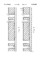
- FIG. 1 is a side view of a MMIC.
- FIG. 2 is a side view of a low dielectric polymer overlaying FIG. 1.
- FIG. 3 is a side view of said low dielectric polymer of FIG. 2 being removed in part.
- FIG. 4 is a side view of a ceramic glass coating layer overlaying the structures indicated in FIG. 3.
- FIG. 5 is a side view of said ceramic glass coating layer of FIG. 4 being removed in part.
- FIG. 6 is a side view of the present invention.
- FIG. 7 is a top view of the present invention.
- FIG. 8 is a graph of the measured results of a x-band LNA both before and after 10 ⁇ m of low dielectric polymer is applied to a MMIC.
- FIG. 9 wherein the curves are shifted about 1 GHz lower in frequency with a slight drop in gain of 0.75 dB.
- FIG. 10 wherein the curves are shifted about 1 GHz lower in frequency with a slight drop in gain of 0.75 dB.
- FIG. 11 wherein the curves are shifted about 1 GHz lower in frequency with a slight drop in gain of 0.75 dB.
- FIG. 12 is a graph of simulated results of the x-band LNA of FIG. 10 both before and after 10.0 ⁇ m of low dielectric polymer coating is applied wherein the graph also shows about a 1 GHz shift in frequency toward the lower end of the band.
- FIG. 13 is a graph of simulated results of the x-band LNA of FIG. 11 both before and after 10.0 ⁇ m of low dielectric polymer coating is applied wherein the graph also slows about a 1 GHz shift in frequency toward the lower end of the band.
- a coating process comprises applying a sufficient coating of a low dielectric polymer 10 upon a processed MMIC board 2 comprising of conventional board material, such as glass, gallium arsenide or quartz.
- the board 3 is gallium arsenide or semi-insulating gallium arsenide.
- the processed board MMIC board has various components, such as airbridges 3, capacitators 4, streets 5, bond pads 6, and field effect transistors 7 (FET) overlying and attached to the board 2.
- the polymer 10 is removed from all bond pads 6 and streets 5 of the MMIC board 10, as illustrated in FIG. 3, by first photoexposing the polymer through a negative mask (not shown), and then rinsing the polymer with a conventional polymeric solvent, such as the Stoddard solvent (not shown). Thereby, the polymer remains in predetermined areas.
- the low dielectric polymer is then cured at a low temperature upon the processed MMIC board.
- a ceramic glass coating 20 overlays the processed MMIC board and low dielectric polymer.
- the ceramic glass coating is removed from the bond pads and streets by applying a positive photoresist material upon the preselected areas of the polymeric coated MMIC.
- the ceramic glass coating is exposed and then the resist material, like A2 5200, and the photoexposed areas of the ceramic glass material are etched using conventional reative ion etching techniques, as illustrated in FIG. 5.
- FIG. 6 illustrates, the polymeric and ceramic glass coated processed MMIC is finished by backside processing procedures.
- FIG. 7 merely illustrates the top side of the finished MMIC wafer having a polymeric coating overlayed by a ceramic glass coating.
- the low dielectric polymer possesses mechanical, electrical and chemical properties that make it compatible with MMIC fabrication processes.
- the low dielectric polymer is preferably spin-coatable and photo-imageable so the polymer can be patterned using simple photolithography.
- the polymer would preferably have a low loss tangent, like 0.002 at 10 Ghz result in minimum perturbation in the microwave performance of the overlayed MMIC.
- Such low dielectric polymers such as an arylcyclobutene like benzocyclobutene or those incorporated by reference in U.S. Pat. No. 5,171,824, having dielectric permittivity ranging below 3.0, preferably below 2.0.
- the low dielectric polymer provides sufficient resistance to moisture. This sufficiency resistance to moisture is increased by overlaying a ceramic-glass layer, like SiC, upon the low dielectric polymer and other pre-determined areas.
- the process of encapsulating the MMIC entails spinning upon the MMIC a uniform coat of the photosensitive, low dielectric polymer and then photo pattern the polymer so that predetermined areas are coated, and other areas like bond pads and wafer streets upon the MMIC are open.
- the uniform coating is sufficiently thick to cover the tallest structure on the MMIC, such as air bridges, which usually require about 10-20 microns of the polymer.
- the polymer is then cured at 250° C. in a vacuum oven under a nitrogen atmosphere for about an hour. After curing the polymer, the ceramic glass layer is deposited upon the polymer and the remaining portions of the MMIC by Plasma Enhanced Chemical Vapor Deposition (PECVD) at 250° C. as referenced in M.
- PECVD Plasma Enhanced Chemical Vapor Deposition
Abstract
Description
              TABLE 1
______________________________________
FET Model Parameters Before and After 10 μm BCB Layer
0.5 × 300 μm; Control FET in ()
Vds = 3 Volts; 25% Idss
FET Model     Before  Difference Percent
Parameters    BCB     after BCB  difference
______________________________________
Ftau (GHz)    26.6    -1.10      -4.2 (-0.7)
Gm (mS/mm)    186     -2.47      -1.4 (-0.4)
Gm.sub.-- DC (mS/mm)
              161     3.37       -2.1 (0.1)
Tau (pSec)    4.11    -0.26      -6.1 (-3.4)
Rd (Ohms*mm)  1.155   0.000       0.0 (0.0)
Rs (Ohms*mm)  0.788   -0.003     -0.3 (-1.2)
Cgs (pF/mm)   1.129   0.036       3.2 (0.0)
Cgd (pF/mm)   0.139   0.034      25.0 (-0.9)
Cds (pF/mm)   0.189   0.051      26.7 (1.2)
Idss (mA/mm)  209     -2.2       -1.0 (0.0)
Vp (Volts)    -1.22   0.0         0.0 (-0.6)
______________________________________
              TABLE 2
______________________________________
Inductor Model Parameters Before and After 10 μm BCB layer
LB23 11 Segments; 2.5 Turns
W = 15 μm; Space = 6 μm; 300 μm Square
4 mil Substrates; Control wafer in ()
Inductor Model
             Before  Difference   Percent
Parameters   BCB     after BCB    difference
______________________________________
L (nH)       2.767   -0.071        -2.6 (-2.2)
Q            41.2    5.0           12.1 (14.6)
C1 (pF)      0.078   0.002         3.0 (1.8)
C2 (pF)      0.065   0.002         3.8 (3.5)
Cp (pF)      0.006   0.007        112.0 (10.2)
______________________________________
Claims (12)
Priority Applications (2)
| Application Number | Priority Date | Filing Date | Title |
|---|---|---|---|
| US08/863,759 US5914508A (en) | 1995-12-21 | 1997-05-27 | Two layer hermetic-like coating process for on-wafer encapsulation of GaAs MMIC's |
| US09/019,627 US6137125A (en) | 1995-12-21 | 1998-02-06 | Two layer hermetic-like coating for on-wafer encapsulatuon of GaAs MMIC's having flip-chip bonding capabilities |
Applications Claiming Priority (2)
| Application Number | Priority Date | Filing Date | Title |
|---|---|---|---|
| US57652495A | 1995-12-21 | 1995-12-21 | |
| US08/863,759 US5914508A (en) | 1995-12-21 | 1997-05-27 | Two layer hermetic-like coating process for on-wafer encapsulation of GaAs MMIC's |
Related Parent Applications (1)
| Application Number | Title | Priority Date | Filing Date |
|---|---|---|---|
| US57652495A Continuation | 1995-12-21 | 1995-12-21 |
Related Child Applications (1)
| Application Number | Title | Priority Date | Filing Date |
|---|---|---|---|
| US09/019,627 Continuation-In-Part US6137125A (en) | 1995-12-21 | 1998-02-06 | Two layer hermetic-like coating for on-wafer encapsulatuon of GaAs MMIC's having flip-chip bonding capabilities |
Publications (1)
| Publication Number | Publication Date |
|---|---|
| US5914508A true US5914508A (en) | 1999-06-22 |
Family
ID=24304789
Family Applications (1)
| Application Number | Title | Priority Date | Filing Date |
|---|---|---|---|
| US08/863,759 Expired - Lifetime US5914508A (en) | 1995-12-21 | 1997-05-27 | Two layer hermetic-like coating process for on-wafer encapsulation of GaAs MMIC's |
Country Status (1)
| Country | Link |
|---|---|
| US (1) | US5914508A (en) |
Cited By (13)
| Publication number | Priority date | Publication date | Assignee | Title |
|---|---|---|---|---|
| US6137125A (en) * | 1995-12-21 | 2000-10-24 | The Whitaker Corporation | Two layer hermetic-like coating for on-wafer encapsulatuon of GaAs MMIC's having flip-chip bonding capabilities |
| WO2001001485A2 (en) * | 1999-06-29 | 2001-01-04 | Koninklijke Philips Electronics N.V. | A semiconductor device |
| US6285070B1 (en) * | 1995-12-22 | 2001-09-04 | Micron Technology, Inc. | Method of forming semiconductor die with integral decoupling capacitor |
| US6362012B1 (en) | 2001-03-05 | 2002-03-26 | Taiwan Semiconductor Manufacturing Company | Structure of merged vertical capacitor inside spiral conductor for RF and mixed-signal applications |
| US6428886B1 (en) * | 1997-06-02 | 2002-08-06 | International Business Machines Corporation | Method for attenuating thermal sensation when handling objects at non-body temperature |
| US6475889B1 (en) | 2000-04-11 | 2002-11-05 | Cree, Inc. | Method of forming vias in silicon carbide and resulting devices and circuits |
| US6549077B1 (en) * | 2002-02-20 | 2003-04-15 | United Microelectronics Corp. | Integrated inductor for RF transistor |
| US6563192B1 (en) | 1995-12-22 | 2003-05-13 | Micron Technology, Inc. | Semiconductor die with integral decoupling capacitor |
| US6667549B2 (en) | 2002-05-01 | 2003-12-23 | Bridgewave Communications, Inc. | Micro circuits with a sculpted ground plane |
| EP1094506A3 (en) * | 1999-10-18 | 2004-03-03 | Applied Materials, Inc. | Capping layer for extreme low dielectric constant films |
| US6875687B1 (en) | 1999-10-18 | 2005-04-05 | Applied Materials, Inc. | Capping layer for extreme low dielectric constant films |
| US20060065910A1 (en) * | 2000-04-11 | 2006-03-30 | Zoltan Ring | Method of forming vias in silicon carbide and resulting devices and circuits |
| US20090104738A1 (en) * | 2000-04-11 | 2009-04-23 | Cree, Inc. | Method of Forming Vias in Silicon Carbide and Resulting Devices and Circuits |
Citations (9)
| Publication number | Priority date | Publication date | Assignee | Title |
|---|---|---|---|---|
| US4714516A (en) * | 1986-09-26 | 1987-12-22 | General Electric Company | Method to produce via holes in polymer dielectrics for multiple electronic circuit chip packaging |
| US4737236A (en) * | 1986-09-08 | 1988-04-12 | M/A-Com, Inc. | Method of making microwave integrated circuits |
| US4780177A (en) * | 1988-02-05 | 1988-10-25 | General Electric Company | Excimer laser patterning of a novel resist |
| US4783695A (en) * | 1986-09-26 | 1988-11-08 | General Electric Company | Multichip integrated circuit packaging configuration and method |
| US4835704A (en) * | 1986-12-29 | 1989-05-30 | General Electric Company | Adaptive lithography system to provide high density interconnect |
| US4894115A (en) * | 1989-02-14 | 1990-01-16 | General Electric Company | Laser beam scanning method for forming via holes in polymer materials |
| US5154793A (en) * | 1988-09-27 | 1992-10-13 | General Electric Company | Method and apparatus for removing components bonded to a substrate |
| US5461545A (en) * | 1990-08-24 | 1995-10-24 | Thomson-Csf | Process and device for hermetic encapsulation of electronic components |
| US5497033A (en) * | 1993-02-08 | 1996-03-05 | Martin Marietta Corporation | Embedded substrate for integrated circuit modules |
-
1997
- 1997-05-27 US US08/863,759 patent/US5914508A/en not_active Expired - Lifetime
Patent Citations (9)
| Publication number | Priority date | Publication date | Assignee | Title |
|---|---|---|---|---|
| US4737236A (en) * | 1986-09-08 | 1988-04-12 | M/A-Com, Inc. | Method of making microwave integrated circuits |
| US4714516A (en) * | 1986-09-26 | 1987-12-22 | General Electric Company | Method to produce via holes in polymer dielectrics for multiple electronic circuit chip packaging |
| US4783695A (en) * | 1986-09-26 | 1988-11-08 | General Electric Company | Multichip integrated circuit packaging configuration and method |
| US4835704A (en) * | 1986-12-29 | 1989-05-30 | General Electric Company | Adaptive lithography system to provide high density interconnect |
| US4780177A (en) * | 1988-02-05 | 1988-10-25 | General Electric Company | Excimer laser patterning of a novel resist |
| US5154793A (en) * | 1988-09-27 | 1992-10-13 | General Electric Company | Method and apparatus for removing components bonded to a substrate |
| US4894115A (en) * | 1989-02-14 | 1990-01-16 | General Electric Company | Laser beam scanning method for forming via holes in polymer materials |
| US5461545A (en) * | 1990-08-24 | 1995-10-24 | Thomson-Csf | Process and device for hermetic encapsulation of electronic components |
| US5497033A (en) * | 1993-02-08 | 1996-03-05 | Martin Marietta Corporation | Embedded substrate for integrated circuit modules |
Non-Patent Citations (14)
| Title |
|---|
| Case et al., High Performance Microwave Elements for SiGe MMICs, Proc. IEEE/Cornell Conference on Advanced Concepts in High Speed Semiconductor Devices and Circuits Aug. 7 9, 1995, pp. 85 92. * |
| Case et al., High Performance Microwave Elements for SiGe MMICs, Proc. IEEE/Cornell Conference on Advanced Concepts in High Speed Semiconductor Devices and Circuits Aug. 7-9, 1995, pp. 85-92. |
| Concise Chemical & Technical Dictionary Edited by H. Bennett, pp. 573, 279. * |
| IEEE Publication (Publication Title Unknown), "A Photosensitive-BCB on Laminate Technology (MCM-LD)", Publication Date Jan. 5, 1994, pp., 374-386. |
| IEEE Publication (Publication Title Unknown), A Photosensitive BCB on Laminate Technology (MCM LD) , Publication Date Jan. 5, 1994, pp., 374 386. * |
| IEEE Transactions on Components, Hybrids, and Manufacturing Technology ; Processing and Microwave Characterization of Multilevel Interconnects Using Benzocyclobutene Dielectric ; Chinoy et al.; vol. 16, No. 7, Nov. 1993. * |
| IEEE Transactions on Components, Hybrids, and Manufacturing Technology; "Processing and Microwave Characterization of Multilevel Interconnects Using Benzocyclobutene Dielectric"; Chinoy et al.; vol. 16, No. 7, Nov. 1993. |
| International Conference on Multichip Modules; "Processing and Electrical Characterization of Multilayer Metallization For Microwave Applications"; Percy B. Chinoy; Apr. 1995. |
| International Conference on Multichip Modules; Processing and Electrical Characterization of Multilayer Metallization For Microwave Applications ; Percy B. Chinoy; Apr. 1995. * |
| Kaleta, et al., GaAs IC Symposium, IEEE Gallium Arsenide Integrated Circuit Symposium 17th Ann. Tech. Dig. 1995. Oct. 29 to Nov. 1, 1995 (abstract only). * |
| M 4 CMs for Microwave Applications, Feurer et al., ISHM 94 Proceed. * |
| M/A COM Loud & Clear ; Balun Transformers for RF Chip Sets, Mixers and Broadband Impedance Matching; Simon Gay; Feb. 1995. * |
| M/A-COM Loud & Clear; "Balun" Transformers for RF Chip Sets, Mixers and Broadband Impedance Matching; Simon Gay; Feb. 1995. |
| M4 CMs for Microwave Applications, Feurer et al., ISHM '94 Proceed. |
Cited By (26)
| Publication number | Priority date | Publication date | Assignee | Title |
|---|---|---|---|---|
| US6137125A (en) * | 1995-12-21 | 2000-10-24 | The Whitaker Corporation | Two layer hermetic-like coating for on-wafer encapsulatuon of GaAs MMIC's having flip-chip bonding capabilities |
| US6563192B1 (en) | 1995-12-22 | 2003-05-13 | Micron Technology, Inc. | Semiconductor die with integral decoupling capacitor |
| US6285070B1 (en) * | 1995-12-22 | 2001-09-04 | Micron Technology, Inc. | Method of forming semiconductor die with integral decoupling capacitor |
| US6428886B1 (en) * | 1997-06-02 | 2002-08-06 | International Business Machines Corporation | Method for attenuating thermal sensation when handling objects at non-body temperature |
| WO2001001485A2 (en) * | 1999-06-29 | 2001-01-04 | Koninklijke Philips Electronics N.V. | A semiconductor device |
| WO2001001485A3 (en) * | 1999-06-29 | 2001-05-03 | Koninkl Philips Electronics Nv | A semiconductor device |
| US6875687B1 (en) | 1999-10-18 | 2005-04-05 | Applied Materials, Inc. | Capping layer for extreme low dielectric constant films |
| EP1094506A3 (en) * | 1999-10-18 | 2004-03-03 | Applied Materials, Inc. | Capping layer for extreme low dielectric constant films |
| US7125786B2 (en) | 2000-04-11 | 2006-10-24 | Cree, Inc. | Method of forming vias in silicon carbide and resulting devices and circuits |
| US20110108855A1 (en) * | 2000-04-11 | 2011-05-12 | Cree, Inc. | Method of forming vias in silicon carbide and resulting devices and circuits |
| US6515303B2 (en) | 2000-04-11 | 2003-02-04 | Cree, Inc. | Method of forming vias in silicon carbide and resulting devices and circuits |
| US6649497B2 (en) | 2000-04-11 | 2003-11-18 | Cree, Inc. | Method of forming vias in silicon carbide and resulting devices and circuits |
| US10367074B2 (en) | 2000-04-11 | 2019-07-30 | Cree, Inc. | Method of forming vias in silicon carbide and resulting devices and circuits |
| US9490169B2 (en) | 2000-04-11 | 2016-11-08 | Cree, Inc. | Method of forming vias in silicon carbide and resulting devices and circuits |
| US20040241970A1 (en) * | 2000-04-11 | 2004-12-02 | Zoltan Ring | Method of Forming Vias in Silicon Carbide and Resulting Devices and Circuits |
| US6475889B1 (en) | 2000-04-11 | 2002-11-05 | Cree, Inc. | Method of forming vias in silicon carbide and resulting devices and circuits |
| US6946739B2 (en) | 2000-04-11 | 2005-09-20 | Cree, Inc. | Layered semiconductor devices with conductive vias |
| US20060065910A1 (en) * | 2000-04-11 | 2006-03-30 | Zoltan Ring | Method of forming vias in silicon carbide and resulting devices and circuits |
| US8202796B2 (en) | 2000-04-11 | 2012-06-19 | Cree, Inc. | Method of forming vias in silicon carbide and resulting devices and circuits |
| US20090104738A1 (en) * | 2000-04-11 | 2009-04-23 | Cree, Inc. | Method of Forming Vias in Silicon Carbide and Resulting Devices and Circuits |
| US7892974B2 (en) | 2000-04-11 | 2011-02-22 | Cree, Inc. | Method of forming vias in silicon carbide and resulting devices and circuits |
| US20110165771A1 (en) * | 2000-04-11 | 2011-07-07 | Cree, Inc. | Method of forming vias in silicon carbide and resulting devices and circuits |
| US6362012B1 (en) | 2001-03-05 | 2002-03-26 | Taiwan Semiconductor Manufacturing Company | Structure of merged vertical capacitor inside spiral conductor for RF and mixed-signal applications |
| US6486529B2 (en) | 2001-03-05 | 2002-11-26 | Taiwan Semiconductor Manufacturing Company | Structure of merged vertical capacitor inside spiral conductor for RF and mixed-signal applications |
| US6549077B1 (en) * | 2002-02-20 | 2003-04-15 | United Microelectronics Corp. | Integrated inductor for RF transistor |
| US6667549B2 (en) | 2002-05-01 | 2003-12-23 | Bridgewave Communications, Inc. | Micro circuits with a sculpted ground plane |
Similar Documents
| Publication | Publication Date | Title |
|---|---|---|
| US5914508A (en) | Two layer hermetic-like coating process for on-wafer encapsulation of GaAs MMIC's | |
| US6137125A (en) | Two layer hermetic-like coating for on-wafer encapsulatuon of GaAs MMIC's having flip-chip bonding capabilities | |
| US5872393A (en) | RF semiconductor device and a method for manufacturing the same | |
| KR101219619B1 (en) | Method for packaging semiconductors at a wafer level | |
| US6675450B1 (en) | Method of manufacturing and mounting electronic devices to limit the effects of parasitics | |
| KR20100044165A (en) | Method for packaging semiconductors at a wafer level | |
| Sharifi et al. | Characterization of Parylene-N as flexible substrate and passivation layer for microwave and millimeter-wave integrated circuits | |
| US20230133481A1 (en) | Aluminum-based gallium nitride integrated circuits | |
| US6833606B2 (en) | Fabrication of a heterojunction bipolar transistor with integrated MIM capacitor | |
| CN107968035B (en) | Semiconductor device and method for manufacturing the same | |
| US9385075B2 (en) | Glass carrier with embedded semiconductor device and metal layers on the top surface | |
| US8653673B2 (en) | Method for packaging semiconductors at a wafer level | |
| Kaleta et al. | A two layer hermetic-like coating process for on-wafer encapsulation of GaAs MMICs | |
| US20030171001A1 (en) | Method of manufacturing semiconductor devices | |
| Alavi et al. | Toward a flexible and adaptive wireless hub by embedding power amplifier thinned silicon chip and antenna in a polymer foil | |
| De Samber et al. | Low-complexity MCM-D technology with integrated passives for high frequency applications | |
| Chaturvedi et al. | Design and electrical characterization of wafer-level micro-package for GaAs-based RFMEMS switches | |
| Pieters et al. | Advances in microwave MCM‐D technology | |
| Wasige et al. | Air bridge based planar hybrid technology for microwave and millimeterwave applications | |
| Simon et al. | A production ready, 6-18-GHz, 5-b phase shifter with integrated CMOS compatible digital interface circuitry | |
| Yoshida et al. | A new millimeter-wave IC on Si substrate using MBB technology | |
| Vandersmissen et al. | Feedback amplifier based on an embedded HEMT in thin-film multilayer MCM-D technology | |
| Inoue et al. | Three-dimensional MMIC interconnect process using photosensitive BCB and STO capacitors | |
| Black et al. | LASER-DIRECT-WRITING TECHNIQUES FOR TUNING AND MODIFICATION OF INTERCONNECTIONS ON INTEGRATED AND MULTIPLE-CHIP CIRCUITS | |
| JPH02128449A (en) | Manufacture of semiconductor device |
Legal Events
| Date | Code | Title | Description |
|---|---|---|---|
| AS | Assignment |
Owner name: AIR FORCE, UNITED STATES, VIRGINIA Free format text: CONFIRMATORY LICENSE;ASSIGNOR:M/A - COM, A DIVISION OF AMP INCORPORATED;REEL/FRAME:009606/0573 Effective date: 19980923 |
|
| STCF | Information on status: patent grant |
Free format text: PATENTED CASE |
|
| CC | Certificate of correction | ||
| FPAY | Fee payment |
Year of fee payment: 4 |
|
| FPAY | Fee payment |
Year of fee payment: 8 |
|
| AS | Assignment |
Owner name: COBHAM DEFENSE ELECTRONIC SYSTEMS CORPORATION, MAS Free format text: ASSIGNMENT OF ASSIGNORS INTEREST;ASSIGNORS:M/A COM, INC.;RAYCHEM INTERNATIONAL;TYCO ELECTRONICS CORPORATION;AND OTHERS;REEL/FRAME:022266/0400;SIGNING DATES FROM 20080108 TO 20090113 Owner name: COBHAM DEFENSE ELECTRONIC SYSTEMS CORPORATION,MASS Free format text: ASSIGNMENT OF ASSIGNORS INTEREST;ASSIGNORS:M/A COM, INC.;RAYCHEM INTERNATIONAL;TYCO ELECTRONICS CORPORATION;AND OTHERS;SIGNING DATES FROM 20080108 TO 20090113;REEL/FRAME:022266/0400 Owner name: COBHAM DEFENSE ELECTRONIC SYSTEMS CORPORATION, MAS Free format text: ASSIGNMENT OF ASSIGNORS INTEREST;ASSIGNORS:M/A COM, INC.;RAYCHEM INTERNATIONAL;TYCO ELECTRONICS CORPORATION;AND OTHERS;SIGNING DATES FROM 20080108 TO 20090113;REEL/FRAME:022266/0400 |
|
| AS | Assignment |
Owner name: COBHAM DEFENSE ELECTRONIC SYSTEMS CORPORATION, MAS Free format text: SECURITY AGREEMENT;ASSIGNOR:KIWI STONE ACQUISITION CORP.;REEL/FRAME:022482/0016 Effective date: 20090330 Owner name: COBHAM DEFENSE ELECTRONIC SYSTEMS CORPORATION,MASS Free format text: SECURITY AGREEMENT;ASSIGNOR:KIWI STONE ACQUISITION CORP.;REEL/FRAME:022482/0016 Effective date: 20090330 |
|
| AS | Assignment |
Owner name: KIWI STONE ACQUISITION CORPORATION, CALIFORNIA Free format text: ASSIGNMENT OF ASSIGNORS INTEREST;ASSIGNOR:COBHAM DEFENSE ELECTRONIC SYSTEMS CORPORATION;REEL/FRAME:022714/0890 Effective date: 20090521 Owner name: KIWI STONE ACQUISITION CORPORATION,CALIFORNIA Free format text: ASSIGNMENT OF ASSIGNORS INTEREST;ASSIGNOR:COBHAM DEFENSE ELECTRONIC SYSTEMS CORPORATION;REEL/FRAME:022714/0890 Effective date: 20090521 |
|
| AS | Assignment |
Owner name: M/A-COM TECHNOLOGY SOLUTIONS HOLDINGS, INC., MASSA Free format text: CHANGE OF NAME;ASSIGNOR:KIWI STONE ACQUISITION CORP.;REEL/FRAME:023476/0069 Effective date: 20090526 Owner name: M/A-COM TECHNOLOGY SOLUTIONS HOLDINGS, INC.,MASSAC Free format text: CHANGE OF NAME;ASSIGNOR:KIWI STONE ACQUISITION CORP.;REEL/FRAME:023476/0069 Effective date: 20090526 |
|
| AS | Assignment |
Owner name: RBS BUSINESS CAPITAL, A DIVISION OF RBS ASSET FINA Free format text: SECURITY AGREEMENT;ASSIGNORS:MIMIX BROADBAND, INC.;M/A-COM TECHNOLOGY SOLUTIONS HOLDINGS, INC.;REEL/FRAME:025444/0920 Effective date: 20101203 |
|
| FPAY | Fee payment |
Year of fee payment: 12 |
|
| AS | Assignment |
Owner name: JPMORGAN CHASE BANK, N.A., AS ADMINISTRATIVE AGENT Free format text: SECURITY AGREEMENT;ASSIGNOR:M/A-COM TECHNOLOGY SOLUTIONS HOLDINGS, INC.;REEL/FRAME:027015/0444 Effective date: 20110930 |
|
| AS | Assignment |
Owner name: M/A-COM TECHNOLOGY SOLUTIONS HOLDINGS, INC., MASSA Free format text: RELEASE OF SECURITY INTEREST RECORDED AT REEL/FRAME 25444/920;ASSIGNOR:RBS BUSINESS CAPITAL, A DIVISION OF RBS ASSET FINANCE, INC., AS ADMINISTRATIVE AGENT;REEL/FRAME:027028/0021 Effective date: 20110930 Owner name: MIMIX BROADBAND, INC., MASSACHUSETTS Free format text: RELEASE OF SECURITY INTEREST RECORDED AT REEL/FRAME 25444/920;ASSIGNOR:RBS BUSINESS CAPITAL, A DIVISION OF RBS ASSET FINANCE, INC., AS ADMINISTRATIVE AGENT;REEL/FRAME:027028/0021 Effective date: 20110930 |
|
| AS | Assignment |
Owner name: JPMORGAN CHASE BANK, N.A., AS ADMINISTRATIVE AGENT Free format text: SECURITY AGREEMENT;ASSIGNOR:M/A-COM TECHNOLOGY SOLUTIONS HOLDINGS, INC.;REEL/FRAME:031314/0183 Effective date: 20130926 |
|
| AS | Assignment |
Owner name: M/A-COM TECHNOLOGY SOLUTIONS HOLDINGS, INC., MASSA Free format text: RELEASE BY SECURED PARTY;ASSIGNOR:JPMORGAN CHASE BANK, N.A.;REEL/FRAME:032857/0032 Effective date: 20140508 |
|
| AS | Assignment |
Owner name: GOLDMAN SACHS BANK USA, NEW YORK Free format text: SECURITY INTEREST;ASSIGNORS:M/A-COM TECHNOLOGY SOLUTIONS HOLDINGS, INC.;MINDSPEED TECHNOLOGIES, INC.;BROOKTREE CORPORATION;REEL/FRAME:032859/0374 Effective date: 20140508 |