US5900163A - Methods for performing plasma etching operations on microelectronic structures - Google Patents
Methods for performing plasma etching operations on microelectronic structures Download PDFInfo
- Publication number
- US5900163A US5900163A US08/784,958 US78495897A US5900163A US 5900163 A US5900163 A US 5900163A US 78495897 A US78495897 A US 78495897A US 5900163 A US5900163 A US 5900163A
- Authority
- US
- United States
- Prior art keywords
- layer
- gas
- etching
- compound
- plasma
- Prior art date
- Legal status (The legal status is an assumption and is not a legal conclusion. Google has not performed a legal analysis and makes no representation as to the accuracy of the status listed.)
- Expired - Fee Related
Links
Images


Classifications
-
- H—ELECTRICITY
- H01—ELECTRIC ELEMENTS
- H01L—SEMICONDUCTOR DEVICES NOT COVERED BY CLASS H10
- H01L21/00—Processes or apparatus adapted for the manufacture or treatment of semiconductor or solid state devices or of parts thereof
- H01L21/02—Manufacture or treatment of semiconductor devices or of parts thereof
- H01L21/04—Manufacture or treatment of semiconductor devices or of parts thereof the devices having at least one potential-jump barrier or surface barrier, e.g. PN junction, depletion layer or carrier concentration layer
- H01L21/18—Manufacture or treatment of semiconductor devices or of parts thereof the devices having at least one potential-jump barrier or surface barrier, e.g. PN junction, depletion layer or carrier concentration layer the devices having semiconductor bodies comprising elements of Group IV of the Periodic System or AIIIBV compounds with or without impurities, e.g. doping materials
- H01L21/30—Treatment of semiconductor bodies using processes or apparatus not provided for in groups H01L21/20 - H01L21/26
- H01L21/302—Treatment of semiconductor bodies using processes or apparatus not provided for in groups H01L21/20 - H01L21/26 to change their surface-physical characteristics or shape, e.g. etching, polishing, cutting
- H01L21/306—Chemical or electrical treatment, e.g. electrolytic etching
- H01L21/3065—Plasma etching; Reactive-ion etching
-
- H—ELECTRICITY
- H01—ELECTRIC ELEMENTS
- H01L—SEMICONDUCTOR DEVICES NOT COVERED BY CLASS H10
- H01L21/00—Processes or apparatus adapted for the manufacture or treatment of semiconductor or solid state devices or of parts thereof
- H01L21/02—Manufacture or treatment of semiconductor devices or of parts thereof
- H01L21/04—Manufacture or treatment of semiconductor devices or of parts thereof the devices having at least one potential-jump barrier or surface barrier, e.g. PN junction, depletion layer or carrier concentration layer
- H01L21/18—Manufacture or treatment of semiconductor devices or of parts thereof the devices having at least one potential-jump barrier or surface barrier, e.g. PN junction, depletion layer or carrier concentration layer the devices having semiconductor bodies comprising elements of Group IV of the Periodic System or AIIIBV compounds with or without impurities, e.g. doping materials
- H01L21/30—Treatment of semiconductor bodies using processes or apparatus not provided for in groups H01L21/20 - H01L21/26
- H01L21/31—Treatment of semiconductor bodies using processes or apparatus not provided for in groups H01L21/20 - H01L21/26 to form insulating layers thereon, e.g. for masking or by using photolithographic techniques; After treatment of these layers; Selection of materials for these layers
- H01L21/3205—Deposition of non-insulating-, e.g. conductive- or resistive-, layers on insulating layers; After-treatment of these layers
- H01L21/321—After treatment
- H01L21/3213—Physical or chemical etching of the layers, e.g. to produce a patterned layer from a pre-deposited extensive layer
- H01L21/32133—Physical or chemical etching of the layers, e.g. to produce a patterned layer from a pre-deposited extensive layer by chemical means only
- H01L21/32135—Physical or chemical etching of the layers, e.g. to produce a patterned layer from a pre-deposited extensive layer by chemical means only by vapour etching only
- H01L21/32136—Physical or chemical etching of the layers, e.g. to produce a patterned layer from a pre-deposited extensive layer by chemical means only by vapour etching only using plasmas
- H01L21/32137—Physical or chemical etching of the layers, e.g. to produce a patterned layer from a pre-deposited extensive layer by chemical means only by vapour etching only using plasmas of silicon-containing layers
Definitions
- the present invention relates to the field of microelectronics and more particularly to manufacturing methods and systems for microelectronic structures.
- microelectronic elements As the capacity and functionality of integrated circuit microelectronic devices increase, the integration of microelectronic elements is also increased. In other words, a number of microelectronic elements fabricated per unit area of a microelectronic substrate is increased. Accordingly, manufacturing techniques must be able to provide high resolution patterns. In particular, dry etching techniques such as plasma fusion etching have been used to achieve high resolution patterns.
- Plasma etching processes can be difficult to control.
- important characteristics of the etching process include the etch profile, the etch selectivity with respect to a lower layer of the microelectronic structure, the etch rate, and the etch uniformity. These etch characteristics depend primarily on the characteristics of the etching apparatus, and the process gases. In particular, the etch uniformity is primarily dependent on the characteristics of the etching apparatus, while the etch profile, etch selectivity, and etch rate are primarily dependent on the process gases used.
- One technique for improving the etching profile is to add a gas which forms a polymer to the gas mixture.
- the added gas allows the plasma etching process to achieve high resolution patterns.
- this technique has been described in "VLSI Technology" by S. M. Sze (2nd Edition, McGraw Hill Press, 1988, pp. 200-204), and U.S. Pat. No. 4,490,209 entitled “Plasma Etching Using Hydrogen Bromide Addition” to Hartman.
- a halogen compound containing fluorine (F) or chlorine (Cl) is provided as a main etching gas.
- the choice of the compound used for the main etching gas is dependent on the properties of the layer to be etched, the desired etching profile, etching selectivity with respect to another layer of the microelectronic structure, and compatibility with other process gases. Additional process gases can be mixed with the main etching gas. These additional gases have predetermined functions.
- inert gases such as helium (He) and argon (Ar) with relatively heavy masses, can act as a carrier for the main etching gas.
- Oxygen (O 2 ) and nitrogen (N 2 ) can be provided and converted to a radical state (O and N) or converted to an ionic state (O 2 + and N 2 + ) by the plasma discharge.
- the radical and ionic states of oxygen and nitrogen can be used to control the etching profile by increasing or decreasing the polymers which are generated during the etching process.
- FIGS. 1A and 1B are photographs illustrating a polysilicon layer which has been etched by a conventional plasma etching technique using a mixture of gases including chlorine, hydrogen bromide, oxygen, and argon. As shown in FIGS. 1A and 1B the profile of the etched polysilicon layer is approximately a reverse trapezoid, and the etched perpendicular plane is tilted.
- etching a layer of a microelectronic structure including the steps of mixing an etching gas with an additional gas which generates an intermediate compound having a carbene structure when exposed to a plasma discharge.
- a plasma is generated to etch exposed portions of the layer, and also to form the intermediate compound having the carbene structure.
- a polymer is formed from the intermediate compound having the carbene structure on the sidewalls of the etched portions of the layer. This polymer acts as a passivation for the sidewalls thus improving the perpendicularity of the sidewalls and the overall profile of the etched layer.
- the etching gas can be a gas including chlorine such as Cl 2 , BCl, HCl, or SiCl 4 .
- the etching gas can be a gas including fluorine such as F 2 , SF 6 , CF 4 and CHF 3 . Mixtures of the above mentioned etching gases can also be used.
- An inert gas such as helium or argon can also be mixed with the etching gas and the additional gas. By generating a plasma of the inert gas, the inert gas is activated. The inert gas thus collides with exposed portions of a layer being etched to remove etch by-products. In particular, the collision of the inert gas can be used to remove polymers which may form on the bottom etching surface. Accordingly, the formation of polymers does not significantly affect the desired etching of the bottom etch surface.
- the additional gas which generates the intermediate compound can be chosen from the group consisting of CH 3 Br, CH 2 Br 2 , CHBr 3 , C 2 H 5 Br, C 2 H 4 Br 2 , or a mixture thereof.
- the resulting intermediate compound having the carbene structure can be C x H y Br z wherein each of x, y, and z is an integer having a value of 0 or greater.
- the intermediate compound can be a compound such as hydrogen bromide carbene (CHBr), dihydrogen carbene (CH 2 ), and dibromocarbene (CBr 2 ). If bromomethane (CH 3 Br) is used as the additional gas, the steps of generating the plasma and forming the polymer can be performed at room temperature.
- oxygen can be provided with the etching gas, and the additional gas and a plasma of the oxygen can be generated.
- the use of oxygen may increase the selectivity of the etch of the polysilicon layer with respect to the silicon oxide layer. More particularly, the ratio of the etching gas to the oxygen can be on the order of 2:1 to 6:1.
- the plasma can be generated by inductive or capacitive coupling or other known techniques.
- a method for etching a layer of a material including silicon on a microelectronic structure can include the steps of masking the layer of the material including silicon so that predetermined portions of layer are exposed, providing an etching gas, and providing an additional gas wherein the additional gas comprises an atom of bromine bonded with another halogen atom.
- a plasma of the etching gas and the additional gas can be generated to etch exposed portions of the layer, and a protective polymer layer can be formed on sidewalls of the etch portions of the layer.
- the additional gas can be chosen from the group consisting of BrI and Br 2 .
- another method for etching a layer of a material including silicon on a microelectronic structure.
- This method includes the steps of masking a layer to be etched so that predetermined portions of a layer are exposed, providing an etching gas, and providing an additional gas wherein the additional gas comprises boron tribromide (BBr 3 ).
- a plasma of etching gas and the additional gas is generated to thereby etch the exposed portions of a layer, and to form a protective polymer layer on sidewalls of the etched portions of the layer.
- the step of generating the plasma can include producing bromine and boron bromide which etch the layer of the material including silicon.
- the plasma etching methods of the present invention can thus be used to produce etched layers having improved sidewall perpendicularity and improved overall profiles.
- the use of a gas which generates an intermediate compound having a carbene structure when exposed to plasma discharge allows the formation of a polymer on sidewalls of the etched portions of the layer which protect the sidewalls during the etching process.
- FIGS. 1A and 1B are photographs illustrating the etch profile a layer of material including silicon which has been etched according to a conventional plasma etching method.
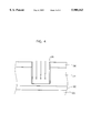
- FIG. 2 is a cross-sectional view of a microelectronic structure which has been etched by a plasma etching method according to the present invention.
- FIGS. 3A and 3B are photographs illustrating etching profiles for a layer of a material including silicon which has been etched by a plasma etching method according to the present invention.
- FIG. 4 is a cross sectional view of a microelectronic structure including a metal layer which has been etched by a plasma etching method according to the present invention.
- Plasma etching methods according to the present invention can be used to etch specific layers of microelectronic structures.
- these plasma etching methods can be used to etch layers of materials including silicon, metal layers, polysilicon layers, and silicon oxide layers.
- the above-mentioned materials can be etched according to the present invention by providing an appropriate mix of gases as discussed below.
- a microelectronic structure includes a substrate 10, a silicon oxide layer 12, a polysilicon layer 14, and a masking layer 16 of photoresist.
- the substrate 10 can be a monocrystalline silicon substrate, and the silicon oxide layer 12 can be on the order of several hundred angstroms.
- the polysilicon layer 14 can be on the order of several thousand angstroms to provide a gate for a transistor.
- the masking layer 16 covers portions of the polysilicon layer 14 which will not be etched.
- An apparatus for performing plasma etching operations can generate a plasma by inductive or capacitive coupling or other known techniques.
- the plasma is inductively generated by winding coils around a quartz tube.
- a diffuser including overlapping sheets or layers can be provided to insure uniform mixing of the etching gas and other process gases.
- the plasma can be generated using a direct current or a radio frequency bias.
- the process temperature can be varied according to the process gases used.
- a main etching gas can be selected from the group of Cl 2 , BCl, HCl, and SiCl 4 , each of which includes chlorine.
- a gas such as CH 3 Br, CH 2 Br 2 , CHBr 3 , C 2 H 5 Br, or C 2 H 4 Br 2 which generates an intermediate compound having a carbene structure when exposed to a plasma discharge is also provided.
- bromomethane CH 3 Br
- control parameters such as vapor pressure can be controlled relatively easily.
- the other gases when generate the intermediate compounds having the carbene structure can be used under varying temperature conditions.
- Oxygen or nitrogen can be supplied to help control etch profiles, and an inert gas such as argon or helium can be provided as a carrier gas.
- the main etching gas can be a compound including fluorine such as F 2 , SF 6 , CF 4 , or CHF 3 .
- a method for etching the polysilicon layer according to the present invention will be discussed using chlorine as the main etching gas.
- the method for etching a polysilicon layer will be discussed using chlorine (CL 2 ) as a main etching gas, bromomethane (CH 3 Br) as the gas which generates the intermediate compound, oxygen (O 2 ) to control the etching profile, and argon (Ar) as the carrier gas.
- chlorine CL 2
- bromomethane CH 3 Br
- oxygen O 2
- argon Ar
- These gases are provided in the reaction chamber and converted to a plasma state by an applied radio frequency signal.
- the chemical reactions are illustrated in the equations listed below. ##STR1## (wherein x is 0 or 1, y and z are each 0 to 2, and Rf means radio frequency)
- the argon or other inert gas is dissociated and activated.
- the activated chlorine from Equation 1 moves to the surface of the polysilicon layer 14 as a result of loading in the argon carrier gas.
- the activated chlorine is bonded to silicon components at the surface of the polysilicon layer 14 as shown in Equation 4 to generate silicon chloride (SiCl).
- the silicon chloride is deposited on the surface of the polysilicon layer 14.
- bromine is generated in the plasma state. This bromine is bonded to silicon components at the surface of the polysilicon layer 14 to form an SiBr polymer which is deposited on the surface of the polysilicon layer as shown in Equation 5.
- C x H y Br z is generated as shown in Equation 2 and this intermediate compound has a carbene (H--C--Br) structure.
- the C x H y Br z is bonded to silicon components at the surface of the polysilicon layer 14 as shown in Equation 6. Accordingly, a polymer bonded in a chain pattern such as C x H y Br z --C x H y Br z is present at the surface of the polysilicon layer and the sidewalls of the profile formed by etching.
- the intermediate compound having the carbene structure is expressed as C x H y Br z wherein x varies from 0 to 1, and y and z each vary from 0 to 2. Accordingly, hydrogen bromide carbene (CHBr), dihydrogen carbene (CH 2 ), and dibromocarbene (CBr 2 ) can be generated and each can form a portion of the polymer.
- the polysilicon layer 14 etched according to the method discussed above is shown in FIGS. 3A and 3B.
- the polysilicon layer is etched by the formation of SiCl and SiBr, and as the polysilicon layer is etched, SiBr and C x H y Br z --C x H y Br z are adsorbed or formed as a polymer on the surface being etched.
- these polymers can be formed on the exposed surfaces of the polysilicon layer 14. These exposed surfaces include the bottom etched surface and the resulting sidewalls.
- the resulting polymer layer 18 which is formed on the sidewalls interrupts the reaction of the silicon at the surface of the sidewalls with the chlorine in the plasma state thus increasing the perpendicularity of the sidewalls with respect to the bottom etch surface. Because the polymer layer 18 reduces the reaction of the silicon at the surface of the sidewalls, over etching of the sidewalls can be reduced and the perpendicularity of the sidewall profile can be enhanced.
- polymers may also form on the bottom etching surface thus interrupting the reaction of the silicon at the bottom etching surface with the chlorine in the plasma state. Accordingly, the polymers may inhibit the desired etching.
- the formation of polymers on the bottom etching surface can be inhibited by the physical sputtering of the activated argon. Accordingly, the effect of polymer formation on the vertical etch rate can be reduced.
- the argon also sputters the masking layer 16 of photoresist. Carbon compounds from the photoresist are thus diffused by the physical sputtering of argon. Because carbon has a relatively high affinity to oxygen, the carbon may bind with oxygen contained in any exposed silicon oxide. Accordingly, when a silicon oxide layer 12 is provided beneath the polysilicon layer 14 being etched as shown in FIG. 2, the carbon may bind with the oxygen of the silicon oxide layer once the polysilicon layer 14 has been etched through. When oxygen of a silicon oxide layer binds with the carbon, etching may continue through the silicon oxide layer 12. Selectivity of the etch with respect to the polysilicon and silicon oxide layers may thus be reduced.
- oxygen can be provided thus reducing the rate at which the silicon oxide layer is etched.
- oxygen is converted to a plasma state including radical (O) and ionic (O 2 + ) states
- the carbon sputtered from the photoresist bonds with the oxygen to generate carbon monoxide (CO) and carbon dioxide (CO 2 ).
- nitrogen can be used to bind the carbon.
- the selectivity of the etch between the polysilicon layer and the silicon oxide layer can be enhanced. If too much oxygen is provided with respect to the amount of chlorine provided, however, the etch of the polysilicon layer may be inhibited. An appropriate quantity of oxygen is thus desired.
- a preferred ratio of chlorine gas to oxygen gas may be on the order of about 2:1 to 6:1.
- the conditions for the etch used to produce the profiles of FIGS. 3A and 3B were as follows. Cl 2 was supplied as the main etching gas, and CH 3 Br, O 2 , and an inert gas were mixed.
- the etching apparatus was configured to provide electrical power on the order of 800-1000 W, bias power on the order of 0-300 W, and total pressure on the order of 2-15 mT.
- the gases were provided at the following rates: Cl 2 was provided at 10-200 sccm; CH 3 Br was provided at 2-100 sccm; O 2 was provided at 0-100 sccm; and the inert gas was provided at 0-200 sccm.
- the unit sccm is a unit of gas supply which represents a standard cubic centimeter of fluid supplied per minute at 0° C. and 1 atmosphere. Furthermore, the temperature of the reaction was maintained in the range of -20 to 60° C.
- FIGS. 3A and 3B illustrate the profiles of polysilicon layers etched by plasma etching methods according to the present invention
- FIGS. 1A and 1B illustrate profiles of polysilicon layers etched according to a conventional method.
- the boundary between the photoresist layer 16 and the polysilicon layer 14 can be maintained as a smooth straight line, and the overall profile of the etched polysilicon layer has an approximately square shape because the sidewalls are formed perpendicular with respect to the bottom etching surface.
- the boundary plane between the photoresist layer 16 and the polysilicon layer 14 is not smooth and straight, and the overall profile of the etched polysilicon has the shape of a reverse-trapezoid because the sidewalls are tilted.
- the profile illustrated in FIGS. 3A and 3B is formed by etching methods of the present invention, and the trenching phenomenon is reduced. Accordingly, the etching methods of the present invention can be used to produce highly-integrated ultra-fine patterns in a polysilicon layer, and the resulting etched polysilicon layer can have smooth surfaces with perpendicular sidewalls as shown in FIGS. 3A and 3B.
- the main etching gas can be a gas including fluorine such as F 2 , SF 6 , CF 4 or CHF 3 .
- an additional gas such as CH 3 Br, CH 2 Br 2 , CHBr 3 , C 2 H 5 Br or C 2 H 4 Br 2 which generates an intermediate compound having a carbene structure when exposed to a plasma discharge can also be used.
- This combination of gases can be used to etch a polysilicon layer or layers of other materials including silicon.
- gases such as oxygen or nitrogen can be used to increase etch selectivity with respect to layers including oxygen, and inert gases such as helium and argon can be used to clear polymers from the bottom etching surface.
- the etching environment can be maintained as discussed above with regard to the etch using gases including chlorine.
- gases including chlorine.
- polymers which form on the sidewalls of the etch layer act as a passivation layer reducing undesired etching of the sidewall and improving the result.
- the second aspect of the etching method of the present invention can be used to provide highly-integrated ultra-fine patterns in polysilicon layers and other layers of materials including silicon.
- a plasma etching method can be used to etch silicon oxide layers.
- the main etching gas can be a gas including fluorine such as F 2 , SF 6 , CF 4 , or CHF 3 .
- An additional gas such as CH 3 Br, CH 2 Br 2 , CHBr 3 , C 2 H 5 Br, or C 2 H 4 Br 2 is used, and the additional gas generates an intermediate compound having a carbene structure when exposed to the plasma discharge.
- other gases such as argon or helium can be added to the mixture to etch the silicon oxide layer.
- a main etching gas is mixed with a gas wherein a bromine atom is bonded with another atom from the halogen group.
- a bromine atom is bonded with another atom from the halogen group.
- BrI or Br 2 can be mixed with the main etching gas to form polymers on the sidewalls of a layer of a material including silicon which is being etched.
- the main etching gas is mixed with BBr 3 as the additional gas to etch a layer of a material including silicon.
- the formation of polymers on the sidewalls of the layer being etched increases the perpendicularity of the sidewalls thus improving the profile of the etched layer.
- a main etching gas can be mixed with an additional gas which generates an intermediate compound having a carbene structure when exposed to the plasma discharge to etch a metal layer.
- polymers form on the sidewalls of the etched layer thus improving the perpendicularity of the sidewalls and improving the profile of the etched layer.
- This method includes masking the metal layer 24 to be etched with an etching mask such as a photoresist mask 26 so that portions of the metal layer 24 are exposed, supplying an etching gas, and supplying an additional gas which generates a compound having a carbene structure when exposed to a plasma discharge.
- a plasma of the etching gas and the additional gas is generated to thereby etch the exposed portions of the metal layer 24 and to form the compound having the carbene structure.
- the etching gas can be an etching gas including chlorine such as Cl 2 , BCl, HCl, and SiCl 4 .
- the generation of the plasma can result in formation of a polymer layer 28 on sidewalls of etched portions of the metal layer 24 wherein the polymer is formed from the compound having the carbene structure.
- the method can also include supplying an inert gas such as helium and/or argon, generating a plasma of said inert gas, and colliding the inert gas with the exposed portion of the metal layer to remove etch by-products.
- the etching gas can also include a gas including fluorine such as F 2 , SF 6 , CF 4 , and CHF 3 .
- the additional gas can include a compound such as CH 3 Br, CH 2 Br 2 , CHBr 3 , C 2 H 5 Br, and C 2 H 4 Br 2
- the intermediate compound having the carbene structure can be C x H y Br z , wherein each of x, y, and z is an integer having a value of zero or greater.
- the compound having the carbene structure can include a compound such as hydrogen bromide carbene (:CHBr), dihydrogen carbene (:CH 2 ), or dibromocarbene (:CBr 2 ).
- the microelectronic structure can include the metal layer 24 to be etched on a layer 22 of silicon oxide (SiO 2 ) opposite the substrate 20, and the method can further include supplying oxygen and generating a plasma of the oxygen.
- the profile of the etched layer can be improved.
- polymers are formed on the sidewalls of the etched layer from the intermediate compound having the carbene structure. These polymer layers provide a passivation for the sidewalls thus improving the perpendicularity of the sidewalls and the overall profile for the etched layer. Ultra-fine highly-integrated patterns can thus be formed by the dry etching methods of the present invention. Accordingly, both the capacity and functionality of integrated circuit devices can be increased.
Abstract
Description
Cl (or Cl.sub.2+)+Si of polysilicon layer→SiCl (4)
Br+Si of polysilicon layer→SiBr (5)
C.sub.x H.sub.y Br.sub.z +Si of polysilicon layer→polymer chain(6)
Claims (26)
Applications Claiming Priority (2)
| Application Number | Priority Date | Filing Date | Title |
|---|---|---|---|
| KR96-15149 | 1996-05-08 | ||
| KR1019960015149A KR100230981B1 (en) | 1996-05-08 | 1996-05-08 | Plasma etching method for manufacturing process of semiconductor device |
Publications (1)
| Publication Number | Publication Date |
|---|---|
| US5900163A true US5900163A (en) | 1999-05-04 |
Family
ID=19458133
Family Applications (1)
| Application Number | Title | Priority Date | Filing Date |
|---|---|---|---|
| US08/784,958 Expired - Fee Related US5900163A (en) | 1996-05-08 | 1997-01-16 | Methods for performing plasma etching operations on microelectronic structures |
Country Status (7)
| Country | Link |
|---|---|
| US (1) | US5900163A (en) |
| JP (1) | JP2807445B2 (en) |
| KR (1) | KR100230981B1 (en) |
| CN (1) | CN1132232C (en) |
| DE (1) | DE19636288B4 (en) |
| GB (1) | GB2313230B (en) |
| TW (1) | TW306026B (en) |
Cited By (133)
| Publication number | Priority date | Publication date | Assignee | Title |
|---|---|---|---|---|
| US6069086A (en) * | 1998-04-30 | 2000-05-30 | Applied Materials, Inc. | Non-HBr shallow trench isolation etch process |
| US6083815A (en) * | 1998-04-27 | 2000-07-04 | Taiwan Semiconductor Manufacturing Company | Method of gate etching with thin gate oxide |
| US6107206A (en) * | 1998-09-14 | 2000-08-22 | Taiwan Semiconductor Manufacturing Company | Method for etching shallow trenches in a semiconductor body |
| WO2001009934A1 (en) * | 1999-08-03 | 2001-02-08 | Applied Materials, Inc. | Sidewall polymer forming gas additives for etching processes |
| US6232219B1 (en) * | 1998-05-20 | 2001-05-15 | Micron Technology, Inc. | Self-limiting method of reducing contamination in a contact opening, method of making contacts and semiconductor devices therewith, and resulting structures |
| US6235214B1 (en) * | 1998-12-03 | 2001-05-22 | Applied Materials, Inc. | Plasma etching of silicon using fluorinated gas mixtures |
| US6306313B1 (en) | 2000-02-04 | 2001-10-23 | Agere Systems Guardian Corp. | Selective etching of thin films |
| US6312616B1 (en) * | 1998-12-03 | 2001-11-06 | Applied Materials, Inc. | Plasma etching of polysilicon using fluorinated gas mixtures |
| US6376383B2 (en) * | 1998-01-16 | 2002-04-23 | Nec Corporation | Method for etching silicon layer |
| US6391790B1 (en) | 2000-05-22 | 2002-05-21 | Applied Materials, Inc. | Method and apparatus for etching photomasks |
| US6492068B1 (en) * | 1999-01-12 | 2002-12-10 | Kawasaki Steel Corporation | Etching method for production of semiconductor devices |
| US6565759B1 (en) * | 1999-08-16 | 2003-05-20 | Vanguard International Semiconductor Corporation | Etching process |
| US6583063B1 (en) | 1998-12-03 | 2003-06-24 | Applied Materials, Inc. | Plasma etching of silicon using fluorinated gas mixtures |
| US6620575B2 (en) * | 1999-02-04 | 2003-09-16 | Applied Materials, Inc | Construction of built-up structures on the surface of patterned masking used for polysilicon etch |
| US20040072081A1 (en) * | 2002-05-14 | 2004-04-15 | Coleman Thomas P. | Methods for etching photolithographic reticles |
| US20040206724A1 (en) * | 2002-09-16 | 2004-10-21 | Applied Materials, Inc. | Method of etching metals with high selectivity to hafnium-based dielectric materials |
| US20040224524A1 (en) * | 2003-05-09 | 2004-11-11 | Applied Materials, Inc. | Maintaining the dimensions of features being etched on a lithographic mask |
| US20040221797A1 (en) * | 2001-10-31 | 2004-11-11 | Aelan Mosden | Method of etching high aspect ratio features |
| US20050029226A1 (en) * | 2003-08-07 | 2005-02-10 | Advanced Power Technology, Inc. | Plasma etching using dibromomethane addition |
| US6872652B2 (en) * | 2001-08-28 | 2005-03-29 | Infineon Technologies Ag | Method of cleaning an inter-level dielectric interconnect |
| US20050175937A1 (en) * | 2004-02-06 | 2005-08-11 | Hynix Semiconductor Inc. | Method for forming fine patterns of semiconductor device |
| US20050181608A1 (en) * | 2000-05-22 | 2005-08-18 | Applied Materials, Inc. | Method and apparatus for etching photomasks |
| US20050255697A1 (en) * | 2001-07-23 | 2005-11-17 | Applied Materials, Inc. | Selective etching of organosilicate films over silicon oxide stop etch layers |
| US20060063386A1 (en) * | 2004-09-23 | 2006-03-23 | Jang-Shiang Tsai | Method for photoresist stripping and treatment of low-k dielectric material |
| US20060094235A1 (en) * | 2004-10-30 | 2006-05-04 | Hynix Semiconductor, Inc. | Method for fabricating gate electrode in semiconductor device |
| US20060138474A1 (en) * | 2004-12-29 | 2006-06-29 | Jae-Seon Yu | Recess gate and method for fabricating semiconductor device with the same |
| US20060166108A1 (en) * | 2005-01-27 | 2006-07-27 | Applied Materials, Inc. | Method for etching a molybdenum layer suitable for photomask fabrication |
| US20070197039A1 (en) * | 2006-02-01 | 2007-08-23 | Alcatel Lucent | Anisotropic etching method |
| US20070218696A1 (en) * | 2006-03-17 | 2007-09-20 | Kenichi Kuwabara | Dry etching method |
| US20090068844A1 (en) * | 2006-04-10 | 2009-03-12 | Solvay Fluor Gmbh | Etching Process |
| US20090087978A1 (en) * | 2007-10-01 | 2009-04-02 | Nanya Technology Corporation | Interconnect manufacturing process |
| US20150332932A1 (en) * | 2014-05-14 | 2015-11-19 | Tokyo Electron Limited | Method for etching etching target layer |
| WO2016060800A1 (en) * | 2013-11-12 | 2016-04-21 | Applied Materials, Inc. | Plasma-free metal etch |
| US9472412B2 (en) | 2013-12-02 | 2016-10-18 | Applied Materials, Inc. | Procedure for etch rate consistency |
| US9478432B2 (en) | 2014-09-25 | 2016-10-25 | Applied Materials, Inc. | Silicon oxide selective removal |
| US9478434B2 (en) | 2014-09-24 | 2016-10-25 | Applied Materials, Inc. | Chlorine-based hardmask removal |
| US9496167B2 (en) | 2014-07-31 | 2016-11-15 | Applied Materials, Inc. | Integrated bit-line airgap formation and gate stack post clean |
| US9493879B2 (en) | 2013-07-12 | 2016-11-15 | Applied Materials, Inc. | Selective sputtering for pattern transfer |
| US9502258B2 (en) | 2014-12-23 | 2016-11-22 | Applied Materials, Inc. | Anisotropic gap etch |
| US9499898B2 (en) | 2014-03-03 | 2016-11-22 | Applied Materials, Inc. | Layered thin film heater and method of fabrication |
| US9553102B2 (en) | 2014-08-19 | 2017-01-24 | Applied Materials, Inc. | Tungsten separation |
| US9564296B2 (en) | 2014-03-20 | 2017-02-07 | Applied Materials, Inc. | Radial waveguide systems and methods for post-match control of microwaves |
| US9576809B2 (en) | 2013-11-04 | 2017-02-21 | Applied Materials, Inc. | Etch suppression with germanium |
| US9607856B2 (en) | 2013-03-05 | 2017-03-28 | Applied Materials, Inc. | Selective titanium nitride removal |
| US9659753B2 (en) | 2014-08-07 | 2017-05-23 | Applied Materials, Inc. | Grooved insulator to reduce leakage current |
| US9659792B2 (en) | 2013-03-15 | 2017-05-23 | Applied Materials, Inc. | Processing systems and methods for halide scavenging |
| US9691645B2 (en) | 2015-08-06 | 2017-06-27 | Applied Materials, Inc. | Bolted wafer chuck thermal management systems and methods for wafer processing systems |
| US9721789B1 (en) | 2016-10-04 | 2017-08-01 | Applied Materials, Inc. | Saving ion-damaged spacers |
| US9728437B2 (en) | 2015-02-03 | 2017-08-08 | Applied Materials, Inc. | High temperature chuck for plasma processing systems |
| US9741593B2 (en) | 2015-08-06 | 2017-08-22 | Applied Materials, Inc. | Thermal management systems and methods for wafer processing systems |
| US9754800B2 (en) | 2010-05-27 | 2017-09-05 | Applied Materials, Inc. | Selective etch for silicon films |
| US9768034B1 (en) | 2016-11-11 | 2017-09-19 | Applied Materials, Inc. | Removal methods for high aspect ratio structures |
| US9773648B2 (en) | 2013-08-30 | 2017-09-26 | Applied Materials, Inc. | Dual discharge modes operation for remote plasma |
| US9842744B2 (en) | 2011-03-14 | 2017-12-12 | Applied Materials, Inc. | Methods for etch of SiN films |
| US9865484B1 (en) | 2016-06-29 | 2018-01-09 | Applied Materials, Inc. | Selective etch using material modification and RF pulsing |
| US9881805B2 (en) | 2015-03-02 | 2018-01-30 | Applied Materials, Inc. | Silicon selective removal |
| US9885117B2 (en) | 2014-03-31 | 2018-02-06 | Applied Materials, Inc. | Conditioned semiconductor system parts |
| US9934942B1 (en) | 2016-10-04 | 2018-04-03 | Applied Materials, Inc. | Chamber with flow-through source |
| US9947549B1 (en) | 2016-10-10 | 2018-04-17 | Applied Materials, Inc. | Cobalt-containing material removal |
| US9966240B2 (en) | 2014-10-14 | 2018-05-08 | Applied Materials, Inc. | Systems and methods for internal surface conditioning assessment in plasma processing equipment |
| US9978564B2 (en) | 2012-09-21 | 2018-05-22 | Applied Materials, Inc. | Chemical control features in wafer process equipment |
| US10026621B2 (en) | 2016-11-14 | 2018-07-17 | Applied Materials, Inc. | SiN spacer profile patterning |
| US10032606B2 (en) | 2012-08-02 | 2018-07-24 | Applied Materials, Inc. | Semiconductor processing with DC assisted RF power for improved control |
| US10043674B1 (en) | 2017-08-04 | 2018-08-07 | Applied Materials, Inc. | Germanium etching systems and methods |
| US10043684B1 (en) | 2017-02-06 | 2018-08-07 | Applied Materials, Inc. | Self-limiting atomic thermal etching systems and methods |
| US10049891B1 (en) | 2017-05-31 | 2018-08-14 | Applied Materials, Inc. | Selective in situ cobalt residue removal |
| US10062587B2 (en) | 2012-07-18 | 2018-08-28 | Applied Materials, Inc. | Pedestal with multi-zone temperature control and multiple purge capabilities |
| US10062578B2 (en) | 2011-03-14 | 2018-08-28 | Applied Materials, Inc. | Methods for etch of metal and metal-oxide films |
| US10062579B2 (en) | 2016-10-07 | 2018-08-28 | Applied Materials, Inc. | Selective SiN lateral recess |
| US10062585B2 (en) | 2016-10-04 | 2018-08-28 | Applied Materials, Inc. | Oxygen compatible plasma source |
| US10062575B2 (en) | 2016-09-09 | 2018-08-28 | Applied Materials, Inc. | Poly directional etch by oxidation |
| US10128086B1 (en) | 2017-10-24 | 2018-11-13 | Applied Materials, Inc. | Silicon pretreatment for nitride removal |
| US10163696B2 (en) | 2016-11-11 | 2018-12-25 | Applied Materials, Inc. | Selective cobalt removal for bottom up gapfill |
| US10170336B1 (en) | 2017-08-04 | 2019-01-01 | Applied Materials, Inc. | Methods for anisotropic control of selective silicon removal |
| US10224210B2 (en) | 2014-12-09 | 2019-03-05 | Applied Materials, Inc. | Plasma processing system with direct outlet toroidal plasma source |
| US10242908B2 (en) | 2016-11-14 | 2019-03-26 | Applied Materials, Inc. | Airgap formation with damage-free copper |
| US10256112B1 (en) | 2017-12-08 | 2019-04-09 | Applied Materials, Inc. | Selective tungsten removal |
| US10256079B2 (en) | 2013-02-08 | 2019-04-09 | Applied Materials, Inc. | Semiconductor processing systems having multiple plasma configurations |
| US10283321B2 (en) | 2011-01-18 | 2019-05-07 | Applied Materials, Inc. | Semiconductor processing system and methods using capacitively coupled plasma |
| US10283324B1 (en) | 2017-10-24 | 2019-05-07 | Applied Materials, Inc. | Oxygen treatment for nitride etching |
| US10297458B2 (en) | 2017-08-07 | 2019-05-21 | Applied Materials, Inc. | Process window widening using coated parts in plasma etch processes |
| US10319739B2 (en) | 2017-02-08 | 2019-06-11 | Applied Materials, Inc. | Accommodating imperfectly aligned memory holes |
| US10319600B1 (en) | 2018-03-12 | 2019-06-11 | Applied Materials, Inc. | Thermal silicon etch |
| US10319649B2 (en) | 2017-04-11 | 2019-06-11 | Applied Materials, Inc. | Optical emission spectroscopy (OES) for remote plasma monitoring |
| US10354889B2 (en) | 2017-07-17 | 2019-07-16 | Applied Materials, Inc. | Non-halogen etching of silicon-containing materials |
| US10403507B2 (en) | 2017-02-03 | 2019-09-03 | Applied Materials, Inc. | Shaped etch profile with oxidation |
| US10424485B2 (en) | 2013-03-01 | 2019-09-24 | Applied Materials, Inc. | Enhanced etching processes using remote plasma sources |
| US10424464B2 (en) | 2015-08-07 | 2019-09-24 | Applied Materials, Inc. | Oxide etch selectivity systems and methods |
| US10431429B2 (en) | 2017-02-03 | 2019-10-01 | Applied Materials, Inc. | Systems and methods for radial and azimuthal control of plasma uniformity |
| US10465294B2 (en) | 2014-05-28 | 2019-11-05 | Applied Materials, Inc. | Oxide and metal removal |
| US10468267B2 (en) | 2017-05-31 | 2019-11-05 | Applied Materials, Inc. | Water-free etching methods |
| US10490406B2 (en) | 2018-04-10 | 2019-11-26 | Appled Materials, Inc. | Systems and methods for material breakthrough |
| US10497573B2 (en) | 2018-03-13 | 2019-12-03 | Applied Materials, Inc. | Selective atomic layer etching of semiconductor materials |
| US10504754B2 (en) | 2016-05-19 | 2019-12-10 | Applied Materials, Inc. | Systems and methods for improved semiconductor etching and component protection |
| US10504700B2 (en) | 2015-08-27 | 2019-12-10 | Applied Materials, Inc. | Plasma etching systems and methods with secondary plasma injection |
| US10522371B2 (en) | 2016-05-19 | 2019-12-31 | Applied Materials, Inc. | Systems and methods for improved semiconductor etching and component protection |
| US10541184B2 (en) | 2017-07-11 | 2020-01-21 | Applied Materials, Inc. | Optical emission spectroscopic techniques for monitoring etching |
| US10541246B2 (en) | 2017-06-26 | 2020-01-21 | Applied Materials, Inc. | 3D flash memory cells which discourage cross-cell electrical tunneling |
| US10546729B2 (en) | 2016-10-04 | 2020-01-28 | Applied Materials, Inc. | Dual-channel showerhead with improved profile |
| US10566206B2 (en) | 2016-12-27 | 2020-02-18 | Applied Materials, Inc. | Systems and methods for anisotropic material breakthrough |
| US10573527B2 (en) | 2018-04-06 | 2020-02-25 | Applied Materials, Inc. | Gas-phase selective etching systems and methods |
| US10573496B2 (en) | 2014-12-09 | 2020-02-25 | Applied Materials, Inc. | Direct outlet toroidal plasma source |
| US10593560B2 (en) | 2018-03-01 | 2020-03-17 | Applied Materials, Inc. | Magnetic induction plasma source for semiconductor processes and equipment |
| US10593523B2 (en) | 2014-10-14 | 2020-03-17 | Applied Materials, Inc. | Systems and methods for internal surface conditioning in plasma processing equipment |
| US10615047B2 (en) | 2018-02-28 | 2020-04-07 | Applied Materials, Inc. | Systems and methods to form airgaps |
| US10629473B2 (en) | 2016-09-09 | 2020-04-21 | Applied Materials, Inc. | Footing removal for nitride spacer |
| US10672642B2 (en) | 2018-07-24 | 2020-06-02 | Applied Materials, Inc. | Systems and methods for pedestal configuration |
| US10679870B2 (en) | 2018-02-15 | 2020-06-09 | Applied Materials, Inc. | Semiconductor processing chamber multistage mixing apparatus |
| US10699879B2 (en) | 2018-04-17 | 2020-06-30 | Applied Materials, Inc. | Two piece electrode assembly with gap for plasma control |
| US10727080B2 (en) | 2017-07-07 | 2020-07-28 | Applied Materials, Inc. | Tantalum-containing material removal |
| US10755941B2 (en) | 2018-07-06 | 2020-08-25 | Applied Materials, Inc. | Self-limiting selective etching systems and methods |
| US10854426B2 (en) | 2018-01-08 | 2020-12-01 | Applied Materials, Inc. | Metal recess for semiconductor structures |
| US10872778B2 (en) | 2018-07-06 | 2020-12-22 | Applied Materials, Inc. | Systems and methods utilizing solid-phase etchants |
| US10886137B2 (en) | 2018-04-30 | 2021-01-05 | Applied Materials, Inc. | Selective nitride removal |
| US10892198B2 (en) | 2018-09-14 | 2021-01-12 | Applied Materials, Inc. | Systems and methods for improved performance in semiconductor processing |
| US10903054B2 (en) | 2017-12-19 | 2021-01-26 | Applied Materials, Inc. | Multi-zone gas distribution systems and methods |
| US10920320B2 (en) | 2017-06-16 | 2021-02-16 | Applied Materials, Inc. | Plasma health determination in semiconductor substrate processing reactors |
| US10920319B2 (en) | 2019-01-11 | 2021-02-16 | Applied Materials, Inc. | Ceramic showerheads with conductive electrodes |
| US10943834B2 (en) | 2017-03-13 | 2021-03-09 | Applied Materials, Inc. | Replacement contact process |
| US10964512B2 (en) | 2018-02-15 | 2021-03-30 | Applied Materials, Inc. | Semiconductor processing chamber multistage mixing apparatus and methods |
| US11049755B2 (en) | 2018-09-14 | 2021-06-29 | Applied Materials, Inc. | Semiconductor substrate supports with embedded RF shield |
| US11062887B2 (en) | 2018-09-17 | 2021-07-13 | Applied Materials, Inc. | High temperature RF heater pedestals |
| US11121002B2 (en) | 2018-10-24 | 2021-09-14 | Applied Materials, Inc. | Systems and methods for etching metals and metal derivatives |
| US11239061B2 (en) | 2014-11-26 | 2022-02-01 | Applied Materials, Inc. | Methods and systems to enhance process uniformity |
| US11257693B2 (en) | 2015-01-09 | 2022-02-22 | Applied Materials, Inc. | Methods and systems to improve pedestal temperature control |
| US11276590B2 (en) | 2017-05-17 | 2022-03-15 | Applied Materials, Inc. | Multi-zone semiconductor substrate supports |
| US11276559B2 (en) | 2017-05-17 | 2022-03-15 | Applied Materials, Inc. | Semiconductor processing chamber for multiple precursor flow |
| US11328909B2 (en) | 2017-12-22 | 2022-05-10 | Applied Materials, Inc. | Chamber conditioning and removal processes |
| US11417534B2 (en) | 2018-09-21 | 2022-08-16 | Applied Materials, Inc. | Selective material removal |
| US11437242B2 (en) | 2018-11-27 | 2022-09-06 | Applied Materials, Inc. | Selective removal of silicon-containing materials |
| US11594428B2 (en) | 2015-02-03 | 2023-02-28 | Applied Materials, Inc. | Low temperature chuck for plasma processing systems |
| US11682560B2 (en) | 2018-10-11 | 2023-06-20 | Applied Materials, Inc. | Systems and methods for hafnium-containing film removal |
| US11721527B2 (en) | 2019-01-07 | 2023-08-08 | Applied Materials, Inc. | Processing chamber mixing systems |
Families Citing this family (14)
| Publication number | Priority date | Publication date | Assignee | Title |
|---|---|---|---|---|
| JP2956602B2 (en) * | 1996-08-26 | 1999-10-04 | 日本電気株式会社 | Dry etching method |
| KR100550348B1 (en) * | 1998-07-22 | 2006-05-17 | 삼성전자주식회사 | Etching Method of Semiconductor Device |
| KR100511929B1 (en) * | 1998-12-15 | 2005-10-26 | 주식회사 하이닉스반도체 | Method for forming contact hole in semiconductor device_ |
| JP2002343798A (en) * | 2001-05-18 | 2002-11-29 | Mitsubishi Electric Corp | Method for dry etching wiring layer, method for manufacturing semiconductor device and semiconductor device obtained in this way |
| KR20030071195A (en) * | 2002-02-28 | 2003-09-03 | 주식회사 하이닉스반도체 | Plasma etch process for semiconductor manufacture |
| US7141505B2 (en) * | 2003-06-27 | 2006-11-28 | Lam Research Corporation | Method for bilayer resist plasma etch |
| EP1793418B1 (en) * | 2004-07-02 | 2013-06-12 | Ulvac, Inc. | Etching method and system |
| KR20120000612A (en) | 2010-06-28 | 2012-01-04 | 삼성전자주식회사 | Method of manufacturing a semiconductor device |
| CN104124148B (en) * | 2013-04-26 | 2017-08-22 | 中微半导体设备(上海)有限公司 | Silicon chip etching method |
| CN104779151B (en) * | 2014-01-13 | 2018-01-26 | 北大方正集团有限公司 | A kind of polycrystalline silicon etching method |
| JP6569578B2 (en) * | 2016-03-30 | 2019-09-04 | 日本ゼオン株式会社 | Plasma etching method |
| CN107910260A (en) * | 2017-11-14 | 2018-04-13 | 扬州扬杰电子科技股份有限公司 | A kind of polysilicon returns carving method |
| US10468527B2 (en) * | 2017-11-15 | 2019-11-05 | Taiwan Semiconductor Manufacturing Co., Ltd. | Metal gate structure and methods of fabricating thereof |
| CN116721915B (en) * | 2023-08-04 | 2023-10-03 | 无锡邑文电子科技有限公司 | SiC etching method and equipment |
Citations (8)
| Publication number | Priority date | Publication date | Assignee | Title |
|---|---|---|---|---|
| US4490209A (en) * | 1983-12-27 | 1984-12-25 | Texas Instruments Incorporated | Plasma etching using hydrogen bromide addition |
| US4789426A (en) * | 1987-01-06 | 1988-12-06 | Harris Corp. | Process for performing variable selectivity polysilicon etch |
| US5126008A (en) * | 1991-05-03 | 1992-06-30 | Applied Materials, Inc. | Corrosion-free aluminum etching process for fabricating an integrated circuit structure |
| US5296095A (en) * | 1990-10-30 | 1994-03-22 | Matsushita Electric Industrial Co., Ltd. | Method of dry etching |
| US5368684A (en) * | 1991-12-19 | 1994-11-29 | Tokyo Electron Limited | Etching method for a silicon-containing layer using hydrogen bromide |
| US5437765A (en) * | 1994-04-29 | 1995-08-01 | Texas Instruments Incorporated | Semiconductor processing |
| US5591301A (en) * | 1994-12-22 | 1997-01-07 | Siemens Aktiengesellschaft | Plasma etching method |
| US5691246A (en) * | 1993-05-13 | 1997-11-25 | Micron Technology, Inc. | In situ etch process for insulating and conductive materials |
Family Cites Families (9)
| Publication number | Priority date | Publication date | Assignee | Title |
|---|---|---|---|---|
| US4855017A (en) * | 1985-05-03 | 1989-08-08 | Texas Instruments Incorporated | Trench etch process for a single-wafer RIE dry etch reactor |
| US4784720A (en) * | 1985-05-03 | 1988-11-15 | Texas Instruments Incorporated | Trench etch process for a single-wafer RIE dry etch reactor |
| US4818334A (en) * | 1988-03-15 | 1989-04-04 | General Electric Company | Method of etching a layer including polysilicon |
| JPH0467624A (en) * | 1990-07-09 | 1992-03-03 | Fujitsu Ltd | Etching process |
| US5169487A (en) * | 1990-08-27 | 1992-12-08 | Micron Technology, Inc. | Anisotropic etch method |
| JPH05102098A (en) * | 1991-10-11 | 1993-04-23 | Sony Corp | Wiring forming method |
| JP3259295B2 (en) * | 1991-10-22 | 2002-02-25 | ソニー株式会社 | Dry etching method and ECR plasma device |
| JP3318777B2 (en) * | 1992-11-17 | 2002-08-26 | ソニー株式会社 | Dry etching method |
| JP3353462B2 (en) * | 1994-06-10 | 2002-12-03 | ソニー株式会社 | Dry etching method |
-
1996
- 1996-05-08 KR KR1019960015149A patent/KR100230981B1/en not_active IP Right Cessation
- 1996-08-30 TW TW085110602A patent/TW306026B/en not_active IP Right Cessation
- 1996-09-06 DE DE19636288A patent/DE19636288B4/en not_active Expired - Fee Related
- 1996-09-10 CN CN96113405A patent/CN1132232C/en not_active Expired - Fee Related
- 1996-09-10 JP JP8260134A patent/JP2807445B2/en not_active Expired - Fee Related
- 1996-11-11 GB GB9623432A patent/GB2313230B/en not_active Expired - Fee Related
-
1997
- 1997-01-16 US US08/784,958 patent/US5900163A/en not_active Expired - Fee Related
Patent Citations (10)
| Publication number | Priority date | Publication date | Assignee | Title |
|---|---|---|---|---|
| US4490209A (en) * | 1983-12-27 | 1984-12-25 | Texas Instruments Incorporated | Plasma etching using hydrogen bromide addition |
| US4490209B1 (en) * | 1983-12-27 | 2000-02-15 | Texas Instruments Inc | Plasma etching using hydrogen bromide addition |
| US4490209B2 (en) * | 1983-12-27 | 2000-12-19 | Texas Instruments Inc | Plasma etching using hydrogen bromide addition |
| US4789426A (en) * | 1987-01-06 | 1988-12-06 | Harris Corp. | Process for performing variable selectivity polysilicon etch |
| US5296095A (en) * | 1990-10-30 | 1994-03-22 | Matsushita Electric Industrial Co., Ltd. | Method of dry etching |
| US5126008A (en) * | 1991-05-03 | 1992-06-30 | Applied Materials, Inc. | Corrosion-free aluminum etching process for fabricating an integrated circuit structure |
| US5368684A (en) * | 1991-12-19 | 1994-11-29 | Tokyo Electron Limited | Etching method for a silicon-containing layer using hydrogen bromide |
| US5691246A (en) * | 1993-05-13 | 1997-11-25 | Micron Technology, Inc. | In situ etch process for insulating and conductive materials |
| US5437765A (en) * | 1994-04-29 | 1995-08-01 | Texas Instruments Incorporated | Semiconductor processing |
| US5591301A (en) * | 1994-12-22 | 1997-01-07 | Siemens Aktiengesellschaft | Plasma etching method |
Non-Patent Citations (2)
| Title |
|---|
| S.M. Sze, VLSI Technology , Second Edition, McGraw Hill Press, 1988, pp. 200 204. * |
| S.M. Sze, VLSI Technology, Second Edition, McGraw-Hill Press, 1988, pp. 200-204. |
Cited By (189)
| Publication number | Priority date | Publication date | Assignee | Title |
|---|---|---|---|---|
| US6376383B2 (en) * | 1998-01-16 | 2002-04-23 | Nec Corporation | Method for etching silicon layer |
| US6083815A (en) * | 1998-04-27 | 2000-07-04 | Taiwan Semiconductor Manufacturing Company | Method of gate etching with thin gate oxide |
| US6069086A (en) * | 1998-04-30 | 2000-05-30 | Applied Materials, Inc. | Non-HBr shallow trench isolation etch process |
| US6232219B1 (en) * | 1998-05-20 | 2001-05-15 | Micron Technology, Inc. | Self-limiting method of reducing contamination in a contact opening, method of making contacts and semiconductor devices therewith, and resulting structures |
| US6400029B1 (en) | 1998-05-20 | 2002-06-04 | Micron Technology, Inc. | Self-limiting method of reducing contamination in a contact opening, method of making contacts and semiconductor devices therewith, and resulting structures |
| US6107206A (en) * | 1998-09-14 | 2000-08-22 | Taiwan Semiconductor Manufacturing Company | Method for etching shallow trenches in a semiconductor body |
| US6583063B1 (en) | 1998-12-03 | 2003-06-24 | Applied Materials, Inc. | Plasma etching of silicon using fluorinated gas mixtures |
| US6235214B1 (en) * | 1998-12-03 | 2001-05-22 | Applied Materials, Inc. | Plasma etching of silicon using fluorinated gas mixtures |
| US6312616B1 (en) * | 1998-12-03 | 2001-11-06 | Applied Materials, Inc. | Plasma etching of polysilicon using fluorinated gas mixtures |
| US6492068B1 (en) * | 1999-01-12 | 2002-12-10 | Kawasaki Steel Corporation | Etching method for production of semiconductor devices |
| US6620575B2 (en) * | 1999-02-04 | 2003-09-16 | Applied Materials, Inc | Construction of built-up structures on the surface of patterned masking used for polysilicon etch |
| WO2001009934A1 (en) * | 1999-08-03 | 2001-02-08 | Applied Materials, Inc. | Sidewall polymer forming gas additives for etching processes |
| US6583065B1 (en) | 1999-08-03 | 2003-06-24 | Applied Materials Inc. | Sidewall polymer forming gas additives for etching processes |
| US6565759B1 (en) * | 1999-08-16 | 2003-05-20 | Vanguard International Semiconductor Corporation | Etching process |
| US6306313B1 (en) | 2000-02-04 | 2001-10-23 | Agere Systems Guardian Corp. | Selective etching of thin films |
| US6534417B2 (en) | 2000-05-22 | 2003-03-18 | Applied Materials, Inc. | Method and apparatus for etching photomasks |
| US7115523B2 (en) | 2000-05-22 | 2006-10-03 | Applied Materials, Inc. | Method and apparatus for etching photomasks |
| US6391790B1 (en) | 2000-05-22 | 2002-05-21 | Applied Materials, Inc. | Method and apparatus for etching photomasks |
| US20050181608A1 (en) * | 2000-05-22 | 2005-08-18 | Applied Materials, Inc. | Method and apparatus for etching photomasks |
| US20050255697A1 (en) * | 2001-07-23 | 2005-11-17 | Applied Materials, Inc. | Selective etching of organosilicate films over silicon oxide stop etch layers |
| US7244672B2 (en) | 2001-07-23 | 2007-07-17 | Applied Materials, Inc. | Selective etching of organosilicate films over silicon oxide stop etch layers |
| US7183201B2 (en) | 2001-07-23 | 2007-02-27 | Applied Materials, Inc. | Selective etching of organosilicate films over silicon oxide stop etch layers |
| US6872652B2 (en) * | 2001-08-28 | 2005-03-29 | Infineon Technologies Ag | Method of cleaning an inter-level dielectric interconnect |
| US7226868B2 (en) | 2001-10-31 | 2007-06-05 | Tokyo Electron Limited | Method of etching high aspect ratio features |
| US20040221797A1 (en) * | 2001-10-31 | 2004-11-11 | Aelan Mosden | Method of etching high aspect ratio features |
| US20040072081A1 (en) * | 2002-05-14 | 2004-04-15 | Coleman Thomas P. | Methods for etching photolithographic reticles |
| US20040206724A1 (en) * | 2002-09-16 | 2004-10-21 | Applied Materials, Inc. | Method of etching metals with high selectivity to hafnium-based dielectric materials |
| US20060060565A9 (en) * | 2002-09-16 | 2006-03-23 | Applied Materials, Inc. | Method of etching metals with high selectivity to hafnium-based dielectric materials |
| US20040224524A1 (en) * | 2003-05-09 | 2004-11-11 | Applied Materials, Inc. | Maintaining the dimensions of features being etched on a lithographic mask |
| WO2005017961A3 (en) * | 2003-08-07 | 2006-05-18 | Advanced Power Technology | Plasma etching using dibromomethane addition |
| WO2005017961A2 (en) * | 2003-08-07 | 2005-02-24 | Advanced Power Technology, Inc. | Plasma etching using dibromomethane addition |
| US20050029226A1 (en) * | 2003-08-07 | 2005-02-10 | Advanced Power Technology, Inc. | Plasma etching using dibromomethane addition |
| US20050175937A1 (en) * | 2004-02-06 | 2005-08-11 | Hynix Semiconductor Inc. | Method for forming fine patterns of semiconductor device |
| US7368226B2 (en) * | 2004-02-06 | 2008-05-06 | Hynix Semiconductor Inc. | Method for forming fine patterns of semiconductor device |
| US20060063386A1 (en) * | 2004-09-23 | 2006-03-23 | Jang-Shiang Tsai | Method for photoresist stripping and treatment of low-k dielectric material |
| US7598176B2 (en) * | 2004-09-23 | 2009-10-06 | Taiwan Semiconductor Manufacturing Co. Ltd. | Method for photoresist stripping and treatment of low-k dielectric material |
| US20060094235A1 (en) * | 2004-10-30 | 2006-05-04 | Hynix Semiconductor, Inc. | Method for fabricating gate electrode in semiconductor device |
| US20060138474A1 (en) * | 2004-12-29 | 2006-06-29 | Jae-Seon Yu | Recess gate and method for fabricating semiconductor device with the same |
| US20060166108A1 (en) * | 2005-01-27 | 2006-07-27 | Applied Materials, Inc. | Method for etching a molybdenum layer suitable for photomask fabrication |
| US8293430B2 (en) | 2005-01-27 | 2012-10-23 | Applied Materials, Inc. | Method for etching a molybdenum layer suitable for photomask fabrication |
| US20070197039A1 (en) * | 2006-02-01 | 2007-08-23 | Alcatel Lucent | Anisotropic etching method |
| US20070218696A1 (en) * | 2006-03-17 | 2007-09-20 | Kenichi Kuwabara | Dry etching method |
| US20090068844A1 (en) * | 2006-04-10 | 2009-03-12 | Solvay Fluor Gmbh | Etching Process |
| US20090087978A1 (en) * | 2007-10-01 | 2009-04-02 | Nanya Technology Corporation | Interconnect manufacturing process |
| US9754800B2 (en) | 2010-05-27 | 2017-09-05 | Applied Materials, Inc. | Selective etch for silicon films |
| US10283321B2 (en) | 2011-01-18 | 2019-05-07 | Applied Materials, Inc. | Semiconductor processing system and methods using capacitively coupled plasma |
| US10062578B2 (en) | 2011-03-14 | 2018-08-28 | Applied Materials, Inc. | Methods for etch of metal and metal-oxide films |
| US9842744B2 (en) | 2011-03-14 | 2017-12-12 | Applied Materials, Inc. | Methods for etch of SiN films |
| US10062587B2 (en) | 2012-07-18 | 2018-08-28 | Applied Materials, Inc. | Pedestal with multi-zone temperature control and multiple purge capabilities |
| US10032606B2 (en) | 2012-08-02 | 2018-07-24 | Applied Materials, Inc. | Semiconductor processing with DC assisted RF power for improved control |
| US10354843B2 (en) | 2012-09-21 | 2019-07-16 | Applied Materials, Inc. | Chemical control features in wafer process equipment |
| US11264213B2 (en) | 2012-09-21 | 2022-03-01 | Applied Materials, Inc. | Chemical control features in wafer process equipment |
| US9978564B2 (en) | 2012-09-21 | 2018-05-22 | Applied Materials, Inc. | Chemical control features in wafer process equipment |
| US11024486B2 (en) | 2013-02-08 | 2021-06-01 | Applied Materials, Inc. | Semiconductor processing systems having multiple plasma configurations |
| US10256079B2 (en) | 2013-02-08 | 2019-04-09 | Applied Materials, Inc. | Semiconductor processing systems having multiple plasma configurations |
| US10424485B2 (en) | 2013-03-01 | 2019-09-24 | Applied Materials, Inc. | Enhanced etching processes using remote plasma sources |
| US9607856B2 (en) | 2013-03-05 | 2017-03-28 | Applied Materials, Inc. | Selective titanium nitride removal |
| US9704723B2 (en) | 2013-03-15 | 2017-07-11 | Applied Materials, Inc. | Processing systems and methods for halide scavenging |
| US9659792B2 (en) | 2013-03-15 | 2017-05-23 | Applied Materials, Inc. | Processing systems and methods for halide scavenging |
| US9493879B2 (en) | 2013-07-12 | 2016-11-15 | Applied Materials, Inc. | Selective sputtering for pattern transfer |
| US9773648B2 (en) | 2013-08-30 | 2017-09-26 | Applied Materials, Inc. | Dual discharge modes operation for remote plasma |
| US9576809B2 (en) | 2013-11-04 | 2017-02-21 | Applied Materials, Inc. | Etch suppression with germanium |
| US9520303B2 (en) | 2013-11-12 | 2016-12-13 | Applied Materials, Inc. | Aluminum selective etch |
| US9472417B2 (en) | 2013-11-12 | 2016-10-18 | Applied Materials, Inc. | Plasma-free metal etch |
| WO2016060800A1 (en) * | 2013-11-12 | 2016-04-21 | Applied Materials, Inc. | Plasma-free metal etch |
| US9711366B2 (en) | 2013-11-12 | 2017-07-18 | Applied Materials, Inc. | Selective etch for metal-containing materials |
| US9472412B2 (en) | 2013-12-02 | 2016-10-18 | Applied Materials, Inc. | Procedure for etch rate consistency |
| US9499898B2 (en) | 2014-03-03 | 2016-11-22 | Applied Materials, Inc. | Layered thin film heater and method of fabrication |
| US9564296B2 (en) | 2014-03-20 | 2017-02-07 | Applied Materials, Inc. | Radial waveguide systems and methods for post-match control of microwaves |
| US9837249B2 (en) | 2014-03-20 | 2017-12-05 | Applied Materials, Inc. | Radial waveguide systems and methods for post-match control of microwaves |
| US9903020B2 (en) | 2014-03-31 | 2018-02-27 | Applied Materials, Inc. | Generation of compact alumina passivation layers on aluminum plasma equipment components |
| US9885117B2 (en) | 2014-03-31 | 2018-02-06 | Applied Materials, Inc. | Conditioned semiconductor system parts |
| US20150332932A1 (en) * | 2014-05-14 | 2015-11-19 | Tokyo Electron Limited | Method for etching etching target layer |
| US9418863B2 (en) * | 2014-05-14 | 2016-08-16 | Tokyo Electron Limited | Method for etching etching target layer |
| US10465294B2 (en) | 2014-05-28 | 2019-11-05 | Applied Materials, Inc. | Oxide and metal removal |
| US9773695B2 (en) | 2014-07-31 | 2017-09-26 | Applied Materials, Inc. | Integrated bit-line airgap formation and gate stack post clean |
| US9496167B2 (en) | 2014-07-31 | 2016-11-15 | Applied Materials, Inc. | Integrated bit-line airgap formation and gate stack post clean |
| US9659753B2 (en) | 2014-08-07 | 2017-05-23 | Applied Materials, Inc. | Grooved insulator to reduce leakage current |
| US9553102B2 (en) | 2014-08-19 | 2017-01-24 | Applied Materials, Inc. | Tungsten separation |
| US9478434B2 (en) | 2014-09-24 | 2016-10-25 | Applied Materials, Inc. | Chlorine-based hardmask removal |
| US9613822B2 (en) | 2014-09-25 | 2017-04-04 | Applied Materials, Inc. | Oxide etch selectivity enhancement |
| US9837284B2 (en) | 2014-09-25 | 2017-12-05 | Applied Materials, Inc. | Oxide etch selectivity enhancement |
| US9478432B2 (en) | 2014-09-25 | 2016-10-25 | Applied Materials, Inc. | Silicon oxide selective removal |
| US10796922B2 (en) | 2014-10-14 | 2020-10-06 | Applied Materials, Inc. | Systems and methods for internal surface conditioning assessment in plasma processing equipment |
| US9966240B2 (en) | 2014-10-14 | 2018-05-08 | Applied Materials, Inc. | Systems and methods for internal surface conditioning assessment in plasma processing equipment |
| US10593523B2 (en) | 2014-10-14 | 2020-03-17 | Applied Materials, Inc. | Systems and methods for internal surface conditioning in plasma processing equipment |
| US10490418B2 (en) | 2014-10-14 | 2019-11-26 | Applied Materials, Inc. | Systems and methods for internal surface conditioning assessment in plasma processing equipment |
| US10707061B2 (en) | 2014-10-14 | 2020-07-07 | Applied Materials, Inc. | Systems and methods for internal surface conditioning in plasma processing equipment |
| US11637002B2 (en) | 2014-11-26 | 2023-04-25 | Applied Materials, Inc. | Methods and systems to enhance process uniformity |
| US11239061B2 (en) | 2014-11-26 | 2022-02-01 | Applied Materials, Inc. | Methods and systems to enhance process uniformity |
| US10573496B2 (en) | 2014-12-09 | 2020-02-25 | Applied Materials, Inc. | Direct outlet toroidal plasma source |
| US10224210B2 (en) | 2014-12-09 | 2019-03-05 | Applied Materials, Inc. | Plasma processing system with direct outlet toroidal plasma source |
| US9502258B2 (en) | 2014-12-23 | 2016-11-22 | Applied Materials, Inc. | Anisotropic gap etch |
| US11257693B2 (en) | 2015-01-09 | 2022-02-22 | Applied Materials, Inc. | Methods and systems to improve pedestal temperature control |
| US10468285B2 (en) | 2015-02-03 | 2019-11-05 | Applied Materials, Inc. | High temperature chuck for plasma processing systems |
| US9728437B2 (en) | 2015-02-03 | 2017-08-08 | Applied Materials, Inc. | High temperature chuck for plasma processing systems |
| US11594428B2 (en) | 2015-02-03 | 2023-02-28 | Applied Materials, Inc. | Low temperature chuck for plasma processing systems |
| US9881805B2 (en) | 2015-03-02 | 2018-01-30 | Applied Materials, Inc. | Silicon selective removal |
| US10607867B2 (en) | 2015-08-06 | 2020-03-31 | Applied Materials, Inc. | Bolted wafer chuck thermal management systems and methods for wafer processing systems |
| US9691645B2 (en) | 2015-08-06 | 2017-06-27 | Applied Materials, Inc. | Bolted wafer chuck thermal management systems and methods for wafer processing systems |
| US10147620B2 (en) | 2015-08-06 | 2018-12-04 | Applied Materials, Inc. | Bolted wafer chuck thermal management systems and methods for wafer processing systems |
| US9741593B2 (en) | 2015-08-06 | 2017-08-22 | Applied Materials, Inc. | Thermal management systems and methods for wafer processing systems |
| US11158527B2 (en) | 2015-08-06 | 2021-10-26 | Applied Materials, Inc. | Thermal management systems and methods for wafer processing systems |
| US10468276B2 (en) | 2015-08-06 | 2019-11-05 | Applied Materials, Inc. | Thermal management systems and methods for wafer processing systems |
| US10424464B2 (en) | 2015-08-07 | 2019-09-24 | Applied Materials, Inc. | Oxide etch selectivity systems and methods |
| US10424463B2 (en) | 2015-08-07 | 2019-09-24 | Applied Materials, Inc. | Oxide etch selectivity systems and methods |
| US11476093B2 (en) | 2015-08-27 | 2022-10-18 | Applied Materials, Inc. | Plasma etching systems and methods with secondary plasma injection |
| US10504700B2 (en) | 2015-08-27 | 2019-12-10 | Applied Materials, Inc. | Plasma etching systems and methods with secondary plasma injection |
| US11735441B2 (en) | 2016-05-19 | 2023-08-22 | Applied Materials, Inc. | Systems and methods for improved semiconductor etching and component protection |
| US10522371B2 (en) | 2016-05-19 | 2019-12-31 | Applied Materials, Inc. | Systems and methods for improved semiconductor etching and component protection |
| US10504754B2 (en) | 2016-05-19 | 2019-12-10 | Applied Materials, Inc. | Systems and methods for improved semiconductor etching and component protection |
| US9865484B1 (en) | 2016-06-29 | 2018-01-09 | Applied Materials, Inc. | Selective etch using material modification and RF pulsing |
| US10629473B2 (en) | 2016-09-09 | 2020-04-21 | Applied Materials, Inc. | Footing removal for nitride spacer |
| US10062575B2 (en) | 2016-09-09 | 2018-08-28 | Applied Materials, Inc. | Poly directional etch by oxidation |
| US9934942B1 (en) | 2016-10-04 | 2018-04-03 | Applied Materials, Inc. | Chamber with flow-through source |
| US9721789B1 (en) | 2016-10-04 | 2017-08-01 | Applied Materials, Inc. | Saving ion-damaged spacers |
| US10541113B2 (en) | 2016-10-04 | 2020-01-21 | Applied Materials, Inc. | Chamber with flow-through source |
| US10224180B2 (en) | 2016-10-04 | 2019-03-05 | Applied Materials, Inc. | Chamber with flow-through source |
| US10546729B2 (en) | 2016-10-04 | 2020-01-28 | Applied Materials, Inc. | Dual-channel showerhead with improved profile |
| US11049698B2 (en) | 2016-10-04 | 2021-06-29 | Applied Materials, Inc. | Dual-channel showerhead with improved profile |
| US10062585B2 (en) | 2016-10-04 | 2018-08-28 | Applied Materials, Inc. | Oxygen compatible plasma source |
| US10062579B2 (en) | 2016-10-07 | 2018-08-28 | Applied Materials, Inc. | Selective SiN lateral recess |
| US10319603B2 (en) | 2016-10-07 | 2019-06-11 | Applied Materials, Inc. | Selective SiN lateral recess |
| US9947549B1 (en) | 2016-10-10 | 2018-04-17 | Applied Materials, Inc. | Cobalt-containing material removal |
| US10163696B2 (en) | 2016-11-11 | 2018-12-25 | Applied Materials, Inc. | Selective cobalt removal for bottom up gapfill |
| US10770346B2 (en) | 2016-11-11 | 2020-09-08 | Applied Materials, Inc. | Selective cobalt removal for bottom up gapfill |
| US10186428B2 (en) | 2016-11-11 | 2019-01-22 | Applied Materials, Inc. | Removal methods for high aspect ratio structures |
| US9768034B1 (en) | 2016-11-11 | 2017-09-19 | Applied Materials, Inc. | Removal methods for high aspect ratio structures |
| US10600639B2 (en) | 2016-11-14 | 2020-03-24 | Applied Materials, Inc. | SiN spacer profile patterning |
| US10026621B2 (en) | 2016-11-14 | 2018-07-17 | Applied Materials, Inc. | SiN spacer profile patterning |
| US10242908B2 (en) | 2016-11-14 | 2019-03-26 | Applied Materials, Inc. | Airgap formation with damage-free copper |
| US10566206B2 (en) | 2016-12-27 | 2020-02-18 | Applied Materials, Inc. | Systems and methods for anisotropic material breakthrough |
| US10431429B2 (en) | 2017-02-03 | 2019-10-01 | Applied Materials, Inc. | Systems and methods for radial and azimuthal control of plasma uniformity |
| US10403507B2 (en) | 2017-02-03 | 2019-09-03 | Applied Materials, Inc. | Shaped etch profile with oxidation |
| US10903052B2 (en) | 2017-02-03 | 2021-01-26 | Applied Materials, Inc. | Systems and methods for radial and azimuthal control of plasma uniformity |
| US10043684B1 (en) | 2017-02-06 | 2018-08-07 | Applied Materials, Inc. | Self-limiting atomic thermal etching systems and methods |
| US10325923B2 (en) | 2017-02-08 | 2019-06-18 | Applied Materials, Inc. | Accommodating imperfectly aligned memory holes |
| US10319739B2 (en) | 2017-02-08 | 2019-06-11 | Applied Materials, Inc. | Accommodating imperfectly aligned memory holes |
| US10529737B2 (en) | 2017-02-08 | 2020-01-07 | Applied Materials, Inc. | Accommodating imperfectly aligned memory holes |
| US10943834B2 (en) | 2017-03-13 | 2021-03-09 | Applied Materials, Inc. | Replacement contact process |
| US10319649B2 (en) | 2017-04-11 | 2019-06-11 | Applied Materials, Inc. | Optical emission spectroscopy (OES) for remote plasma monitoring |
| US11361939B2 (en) | 2017-05-17 | 2022-06-14 | Applied Materials, Inc. | Semiconductor processing chamber for multiple precursor flow |
| US11276590B2 (en) | 2017-05-17 | 2022-03-15 | Applied Materials, Inc. | Multi-zone semiconductor substrate supports |
| US11276559B2 (en) | 2017-05-17 | 2022-03-15 | Applied Materials, Inc. | Semiconductor processing chamber for multiple precursor flow |
| US11915950B2 (en) | 2017-05-17 | 2024-02-27 | Applied Materials, Inc. | Multi-zone semiconductor substrate supports |
| US10468267B2 (en) | 2017-05-31 | 2019-11-05 | Applied Materials, Inc. | Water-free etching methods |
| US10049891B1 (en) | 2017-05-31 | 2018-08-14 | Applied Materials, Inc. | Selective in situ cobalt residue removal |
| US10497579B2 (en) | 2017-05-31 | 2019-12-03 | Applied Materials, Inc. | Water-free etching methods |
| US10920320B2 (en) | 2017-06-16 | 2021-02-16 | Applied Materials, Inc. | Plasma health determination in semiconductor substrate processing reactors |
| US10541246B2 (en) | 2017-06-26 | 2020-01-21 | Applied Materials, Inc. | 3D flash memory cells which discourage cross-cell electrical tunneling |
| US10727080B2 (en) | 2017-07-07 | 2020-07-28 | Applied Materials, Inc. | Tantalum-containing material removal |
| US10541184B2 (en) | 2017-07-11 | 2020-01-21 | Applied Materials, Inc. | Optical emission spectroscopic techniques for monitoring etching |
| US10354889B2 (en) | 2017-07-17 | 2019-07-16 | Applied Materials, Inc. | Non-halogen etching of silicon-containing materials |
| US10043674B1 (en) | 2017-08-04 | 2018-08-07 | Applied Materials, Inc. | Germanium etching systems and methods |
| US10170336B1 (en) | 2017-08-04 | 2019-01-01 | Applied Materials, Inc. | Methods for anisotropic control of selective silicon removal |
| US10593553B2 (en) | 2017-08-04 | 2020-03-17 | Applied Materials, Inc. | Germanium etching systems and methods |
| US11101136B2 (en) | 2017-08-07 | 2021-08-24 | Applied Materials, Inc. | Process window widening using coated parts in plasma etch processes |
| US10297458B2 (en) | 2017-08-07 | 2019-05-21 | Applied Materials, Inc. | Process window widening using coated parts in plasma etch processes |
| US10283324B1 (en) | 2017-10-24 | 2019-05-07 | Applied Materials, Inc. | Oxygen treatment for nitride etching |
| US10128086B1 (en) | 2017-10-24 | 2018-11-13 | Applied Materials, Inc. | Silicon pretreatment for nitride removal |
| US10256112B1 (en) | 2017-12-08 | 2019-04-09 | Applied Materials, Inc. | Selective tungsten removal |
| US10903054B2 (en) | 2017-12-19 | 2021-01-26 | Applied Materials, Inc. | Multi-zone gas distribution systems and methods |
| US11328909B2 (en) | 2017-12-22 | 2022-05-10 | Applied Materials, Inc. | Chamber conditioning and removal processes |
| US10854426B2 (en) | 2018-01-08 | 2020-12-01 | Applied Materials, Inc. | Metal recess for semiconductor structures |
| US10861676B2 (en) | 2018-01-08 | 2020-12-08 | Applied Materials, Inc. | Metal recess for semiconductor structures |
| US10699921B2 (en) | 2018-02-15 | 2020-06-30 | Applied Materials, Inc. | Semiconductor processing chamber multistage mixing apparatus |
| US10679870B2 (en) | 2018-02-15 | 2020-06-09 | Applied Materials, Inc. | Semiconductor processing chamber multistage mixing apparatus |
| US10964512B2 (en) | 2018-02-15 | 2021-03-30 | Applied Materials, Inc. | Semiconductor processing chamber multistage mixing apparatus and methods |
| US10615047B2 (en) | 2018-02-28 | 2020-04-07 | Applied Materials, Inc. | Systems and methods to form airgaps |
| US10593560B2 (en) | 2018-03-01 | 2020-03-17 | Applied Materials, Inc. | Magnetic induction plasma source for semiconductor processes and equipment |
| US11004689B2 (en) | 2018-03-12 | 2021-05-11 | Applied Materials, Inc. | Thermal silicon etch |
| US10319600B1 (en) | 2018-03-12 | 2019-06-11 | Applied Materials, Inc. | Thermal silicon etch |
| US10497573B2 (en) | 2018-03-13 | 2019-12-03 | Applied Materials, Inc. | Selective atomic layer etching of semiconductor materials |
| US10573527B2 (en) | 2018-04-06 | 2020-02-25 | Applied Materials, Inc. | Gas-phase selective etching systems and methods |
| US10490406B2 (en) | 2018-04-10 | 2019-11-26 | Appled Materials, Inc. | Systems and methods for material breakthrough |
| US10699879B2 (en) | 2018-04-17 | 2020-06-30 | Applied Materials, Inc. | Two piece electrode assembly with gap for plasma control |
| US10886137B2 (en) | 2018-04-30 | 2021-01-05 | Applied Materials, Inc. | Selective nitride removal |
| US10872778B2 (en) | 2018-07-06 | 2020-12-22 | Applied Materials, Inc. | Systems and methods utilizing solid-phase etchants |
| US10755941B2 (en) | 2018-07-06 | 2020-08-25 | Applied Materials, Inc. | Self-limiting selective etching systems and methods |
| US10672642B2 (en) | 2018-07-24 | 2020-06-02 | Applied Materials, Inc. | Systems and methods for pedestal configuration |
| US11049755B2 (en) | 2018-09-14 | 2021-06-29 | Applied Materials, Inc. | Semiconductor substrate supports with embedded RF shield |
| US10892198B2 (en) | 2018-09-14 | 2021-01-12 | Applied Materials, Inc. | Systems and methods for improved performance in semiconductor processing |
| US11062887B2 (en) | 2018-09-17 | 2021-07-13 | Applied Materials, Inc. | High temperature RF heater pedestals |
| US11417534B2 (en) | 2018-09-21 | 2022-08-16 | Applied Materials, Inc. | Selective material removal |
| US11682560B2 (en) | 2018-10-11 | 2023-06-20 | Applied Materials, Inc. | Systems and methods for hafnium-containing film removal |
| US11121002B2 (en) | 2018-10-24 | 2021-09-14 | Applied Materials, Inc. | Systems and methods for etching metals and metal derivatives |
| US11437242B2 (en) | 2018-11-27 | 2022-09-06 | Applied Materials, Inc. | Selective removal of silicon-containing materials |
| US11721527B2 (en) | 2019-01-07 | 2023-08-08 | Applied Materials, Inc. | Processing chamber mixing systems |
| US10920319B2 (en) | 2019-01-11 | 2021-02-16 | Applied Materials, Inc. | Ceramic showerheads with conductive electrodes |
Also Published As
| Publication number | Publication date |
|---|---|
| JPH09306895A (en) | 1997-11-28 |
| GB2313230A (en) | 1997-11-19 |
| GB9623432D0 (en) | 1997-01-08 |
| DE19636288A1 (en) | 1997-11-13 |
| CN1164761A (en) | 1997-11-12 |
| KR100230981B1 (en) | 1999-11-15 |
| DE19636288B4 (en) | 2004-02-12 |
| CN1132232C (en) | 2003-12-24 |
| GB2313230B (en) | 1998-07-22 |
| TW306026B (en) | 1997-05-21 |
| JP2807445B2 (en) | 1998-10-08 |
| KR970077307A (en) | 1997-12-12 |
Similar Documents
| Publication | Publication Date | Title |
|---|---|---|
| US5900163A (en) | Methods for performing plasma etching operations on microelectronic structures | |
| US6569773B1 (en) | Method for anisotropic plasma-chemical dry etching of silicon nitride layers using a gas mixture containing fluorine | |
| EP0350997B1 (en) | Reactive ion etching of a silicon-bearing material with hydrogen bromide | |
| KR100274080B1 (en) | Dry etching method | |
| US6008139A (en) | Method of etching polycide structures | |
| JP4579611B2 (en) | Dry etching method | |
| CN1271688C (en) | Plasma etching of silicon carbide | |
| US7361607B2 (en) | Method for multi-layer resist plasma etch | |
| US5078833A (en) | Dry etching method | |
| JP3409313B2 (en) | Anisotropic nitride etching method with high selectivity for oxide and photoresist layers | |
| US6037265A (en) | Etchant gas and a method for etching transistor gates | |
| JPH04350932A (en) | Method of dry etching | |
| US20050026431A1 (en) | LSI device etching method and apparatus thereof | |
| US5851926A (en) | Method for etching transistor gates using a hardmask | |
| US5880033A (en) | Method for etching metal silicide with high selectivity to polysilicon | |
| US5928967A (en) | Selective oxide-to-nitride etch process using C4 F8 /CO/Ar | |
| JP2001517868A (en) | Selective etching plasma treatment of oxides using fluoropropene or fluoropropylene | |
| US6069087A (en) | Highly selective dry etching process | |
| US6565759B1 (en) | Etching process | |
| US5314578A (en) | Process for etching a multi-layer substrate | |
| JP3883144B2 (en) | Manufacturing method of semiconductor device | |
| KR100300512B1 (en) | Anisotropic etching method with high nitride to oxide selectivity | |
| US20050029226A1 (en) | Plasma etching using dibromomethane addition | |
| JP7296912B2 (en) | Substrate processing method and substrate processing apparatus | |
| JPH1154481A (en) | Dry-etching method and dry-etching device |
Legal Events
| Date | Code | Title | Description |
|---|---|---|---|
| AS | Assignment |
Owner name: SAMSUNG ELECTRONICS CO., LTD., KOREA, REPUBLIC OF Free format text: ASSIGNMENT OF ASSIGNORS INTEREST;ASSIGNORS:YI, WHI-KUN;MOON, DAI-SIK;KIM, SUNG-KYEONG;AND OTHERS;REEL/FRAME:008507/0753 Effective date: 19970507 |
|
| FEPP | Fee payment procedure |
Free format text: PAYOR NUMBER ASSIGNED (ORIGINAL EVENT CODE: ASPN); ENTITY STATUS OF PATENT OWNER: LARGE ENTITY |
|
| FPAY | Fee payment |
Year of fee payment: 4 |
|
| FPAY | Fee payment |
Year of fee payment: 8 |
|
| REMI | Maintenance fee reminder mailed | ||
| LAPS | Lapse for failure to pay maintenance fees | ||
| STCH | Information on status: patent discontinuation |
Free format text: PATENT EXPIRED DUE TO NONPAYMENT OF MAINTENANCE FEES UNDER 37 CFR 1.362 |
|
| FP | Lapsed due to failure to pay maintenance fee |
Effective date: 20110504 |