US5864243A - Buffer and method for transferring data therein - Google Patents
Buffer and method for transferring data therein Download PDFInfo
- Publication number
- US5864243A US5864243A US08/715,457 US71545796A US5864243A US 5864243 A US5864243 A US 5864243A US 71545796 A US71545796 A US 71545796A US 5864243 A US5864243 A US 5864243A
- Authority
- US
- United States
- Prior art keywords
- data
- output
- transistor
- input
- signal
- Prior art date
- Legal status (The legal status is an assumption and is not a legal conclusion. Google has not performed a legal analysis and makes no representation as to the accuracy of the status listed.)
- Expired - Lifetime
Links
Images


Classifications
-
- H—ELECTRICITY
- H03—ELECTRONIC CIRCUITRY
- H03K—PULSE TECHNIQUE
- H03K19/00—Logic circuits, i.e. having at least two inputs acting on one output; Inverting circuits
- H03K19/003—Modifications for increasing the reliability for protection
- H03K19/00315—Modifications for increasing the reliability for protection in field-effect transistor circuits
Definitions
- the present invention relates to buffers and methods for transferring data therein.
- Portable personal computers have generated a large demand for low power integrated circuits.
- low power integrated circuits i.e., 3.3 volts
- portable systems such as a laptop personal computer
- 5 volt integrated circuits provide performance advantages over low power 3.3 volt integrated circuits. Therefore, both 5 volt integrated circuits and 3.3 volt integrated circuits may be utilized within a single personal computer.
- An input/output buffer may be utilized intermediate mixed voltage logic circuits.
- 3.3 volt and 5 volt integrated circuits are intermixed within a single device.
- 3.3 volt integrated circuits usually have a thin MOS gate oxide compared with the 5 volt integrated circuit (70A versus 90A).
- the MOS gate oxide of 3.3 volt circuits may become leaky when a 5 volt input signal is applied to it.
- the MOS gate oxide may become leaky due to tunneling effect or time-dependent dielectric breakdown (TDDB) effect.
- TDDB time-dependent dielectric breakdown
- the gate oxide might also be permanently damaged if the electric field in the oxide is larger than its breakdown voltage.
- Another problem is leakage current from a 5 volt pad interconnect to the input/output buffer power supply via a parasitic junction diode of the PMOS transistor.
- a third problem is the leakage current caused by higher static current due to 5 volts on the respective drains of the 3.3 volt powered PMOS and NMOS.
- a final problem is the leakage current from the electrostatic discharge (ESD) protection diode on the driven input buffer.
- ESD electrostatic discharge
- Other reliability issues which may arise with the mixing of 3.3 volt and 5 volt integrated circuits include hot carrier effect and electromigration due to the higher pad voltage (i.e. 5 volts) on the respective drains of the output metal-oxide semiconductor transistors.
- a cascade output NMOS transistor may be utilized to protect an NMOS output transistor of the input/output buffer to eliminate or minimize many of the aforementioned design problems.
- a prior art input/output buffer 10 having an NMOS output transistor 11 and a PMOS output transistor 13 is shown coupled with a pad 14.
- the NMOS output transistor 11 is coupled with a cascade NMOS output transistor 12.
- the channel width and length (W/L) ratio within each of the cascaded NMOS output transistors 11, 12 is doubled (compared to the width and length ratio of a single output NMOS transistor) to maintain the original driving strength.
- the prior art I/O buffer 10 shown in FIG. 1 minimizes some of the design problems and tolerates a 5 volt input data signal on the pad 14.
- the prior art I/O buffer 10 is not a true CMOS buffer inasmuch as its output PMOS transistor 13 and output NMOS transistor 11 are not fully turned off when the output data signal is changed from low to high and high to low, respectively.
- the graph shown in FIG. 2 illustrates that the voltages on the gates of the output NMOS transistor 11 and the output PMOS transistor 13 (represented by respective lines 16 and 17 in FIG. 2) are not equal from before and after switching in response to changes of an output data signal (represented by line 15).
- FIG. 1 is a schematic diagram of a prior art 3 volt/5 volt compatible input/output buffer.
- FIG. 2 is a graphical representation of the gate voltages applied to the transistors within the output driver of the prior art buffer shown in FIG. 1.
- FIG. 3 is a functional block diagram of a buffer according to the present invention interposed between a first logic circuit and a second logic circuit.
- FIG. 4 is a functional block diagram, similar to FIG. 3, of a buffer according to the present invention.
- FIG. 5 is a schematic diagram of a preferred embodiment of an output buffer in accordance with the present invention.
- FIG. 6 is a schematic diagram of a bidirectional buffer showing a preferred embodiment of an input buffer in accordance with the present invention.
- FIG. 7 is a graphical representation of the gate voltages applied to the transistors within the output driver of a buffer according to the present invention.
- the present invention is generally described herein as a Peripheral Component Interconnect Input/Output Buffer, it is to be distinctly understood that the buffer according to the present invention may be utilized for interfacing between general mixed 3.3 volt and 5 volt logic circuits.
- a buffer comprises:
- a data input configured to receive an output data signal
- a data interface configured to couple with a pad interconnect
- an output driver coupled with said data interface and being configured to apply the output data signal thereto;
- a data controller intermediate said data input and said output driver, said data controller being configured to apply a plurality of control signals of substantially equal voltage to said output driver to control the operation thereof responsive to the output data signal received via said data input.
- the buffer comprises:
- a data input configured to receive an output data signal
- a data controller coupled with said data input
- a data interface configured to couple with a pad interconnect
- an output driver including a first output transistor and a second output transistor individually coupled with said data controller
- said data controller applying a first control signal to said first output transistor and a second control signal to said second output transistor, said first control signal and said second control signal having substantially equal voltages, said first output transistor and said second output transistor being operable to apply the output data signal to said data interface.
- a method of transferring data within a buffer comprises:
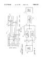
- a bidirectional buffer 30 is shown intermediate a 3.3 volt or first logic circuit 26 and a 5 volt or second logic circuit 27.
- the bidirectional buffer 30 generally comprises an output buffer 32 and an input buffer 34 each coupled with the first logic circuit 26 and the second logic circuit 27.
- a pad interconnect 36 is intermediate the bidirectional buffer 30 and the second logic circuit 27.
- the preferred bidirectional buffer 30 is powered by a 3.3 volt power supply.
- the 3.3 volt power supply is represented as Vdd in FIG. 5 and FIG. 6.
- the preferred bidirectional buffer 30 may be utilized in a mixed 3.3 volt-5 volt signaling environment and is capable of 5 volt tolerance when it operates in an input mode. Additionally, the preferred bidirectional buffer 30 may operate as a true output CMOS buffer which can drive 3.3 volt and 5 volt signaling circuits on the same Peripheral Component Interconnect (PCI) bus.
- PCI Peripheral Component Interconnect
- the bidirectional buffer 30 includes an output enable interface 37, a data input 38 and a data output 39 coupled with the first logic circuit 26.
- the bidirectional buffer 30 in accordance with the present invention additionally includes a data interface 35 which is coupled with the pad interconnect 36.
- the data interface 35 is configured to transfer input data signals and output data signals.
- An output enable signal (also referred to as an OEN signal) is generated within the first logic circuit 26 and is applied to the OEN interface 37 within the bidirectional buffer 30.
- the OEN signal controls the operation of the bidirectional buffer 30 between an input mode and an output mode.
- Output data signals may be transferred from the first logic circuit 26 to the second logic circuit 27 when the bidirectional buffer 30 operates in the output mode.
- Input data signals may be transferred from the second logic circuit 27 to the first logic circuit 26 when the bidirectional buffer 30 operates in an input mode.
- the bidirectional buffer 30 operates in an output mode responsive to the OEN signal being a logic low signal.
- a 3.3 volt output data signal generated within the first logic circuit 26 may enter the buffer 32 via the data input 38.
- the output data signal passes into the output buffer 32 of the bidirectional buffer 30.
- the output buffer 32 applies the output data signal through the data interface 35 to the pad interconnect 36 which is coupled with the second logic circuit 27.
- the bidirectional buffer 30 may drive either a 3.3 volt or 5 volt circuit via the pad interconnect 36.
- the output buffer 32 of the bidirectional buffer 30 operates as a true CMOS output buffer.
- the output buffer 32 includes an output driver 46 for driving the second logic circuit 27 and a data controller 40 for operating the output driver 46 in response to the input data signal.
- the output buffer 32 is shown in detail in FIG. 5.
- the output driver 46 comprises a first output transistor 47 and second output transistor 48.
- the first output transistor 47 is a PMOS transistor and the second output transistor 48 is a NMOS transistor.
- a cascade NMOS transistor 51 is interposed between the second output transistor 48 and the data interface 35.
- the cascade NMOS transistor 51 is utilized to protect the second output transistor 48 in the presence of an input data signal having a voltage which exceeds a predetermined threshold (e.g., 3.3 volts).
- the data controller 40 is coupled with the first output transistor 46 and the second output transistor 47 via a respective first interconnect 49 and second interconnect 50.
- the data controller 40 provides first and second control signals to the output driver 46 to control the generation of the output data signal applied to the second logic circuit 27.
- the data controller 40 generates the first and second control signals in response to the output data signal received via the data input 38.
- the first and second control signals are applied to the respective gate electrodes of the first output transistor 47 and the second output transistor 48.
- the voltages of the two control signals are substantially equal at any given time.
- the voltages of the two control signals are substantially equal as shown in FIG. 7 during switching between logic high and logic low in response to a change in state of the output data signal. Therefore, the output driver 46 only draws current during switching, thereby reducing current leakage and power consumption.
- the bidirectional buffer 30 operates in an input mode when the OEN signal is logic high. As shown in FIG. 3, an input data signal generated within the second logic circuit 27 is applied via the pad interconnect 36 to the data interface 35 of the bidirectional buffer 30. The voltage of the input data signal may be between 0 and 5 volts. The input data signal passes through the input buffer 34 to the first logic circuit 26 via the data output 39. The output driver 46 is in an OFF state responsive to the presence of a logic high OEN signal from the first logic circuit 26.
- the bidirectional buffer 30, in an input mode, may operate in a 3.3 volt to 5 volt signalling environment. More specifically, the bidirectional buffer 30 may tolerate a 5 volt input data signal received via the pad interconnect 36 without incurring excessive leakage current or a gate reliability problem.
- the operation of the output buffer 32 in accordance with the present invention is discussed with reference to FIG. 4 and FIG. 5.
- the first logic circuit 26 generates a logic low output enable signal when data will be outputted to the second logic circuit 27 via the bidirectional buffer 30.
- the logic low OEN signal is received by the OEN interface 37 and subsequently applied to a CMOS inverter 52 as shown in FIG. 5.
- the CMOS inverter 52 outputs a logic high signal (3.3 volts).
- a plurality of transistors, including a first NMOS transistor 55, a second NMOS transistor 56, and a first PMOS transistor 57 control the voltage at a fourth interconnect 54 responsive to the OEN signal.
- the transistors 55, 56, 57 are configured such that the fourth interconnect 54 is 0 volts whenever the OEN signal is logic low.
- the inverted OEN signal from the CMOS inverter 52 is applied to the gate electrode of the first NMOS transistor 55.
- the inverted OEN signal biases the first NMOS transistor 55 in an ON state thereby coupling the fourth interconnect 54 with ground via the second NMOS transistor 56.
- a first isolating transistor 58 and a second isolating transistor 59 are provided within the data controller 40.
- the first isolating transistor 58 and second isolating transistor 59 are intermediate the data input 38 and the first output transistor 47.
- the first isolating transistor 58 is fully open when the fourth interconnect 54 is 0 volts.
- the second isolating transistor 59 is fully open and provides a connection path in parallel with the first isolating transistor 59. Both isolating transistors 58, 59 are operable to pass a control signal to the first output transistor 47 via the first interconnect 49.
- the data controller 40 includes a predriver 41.
- the predriver 41 generates control signals for operating the output transistors 47, 48 in response to the output data signal.
- the output data signal is received into the bidirectional buffer 30 via the data input 38.
- the data input 38 is coupled with the predriver 41 as shown in FIG. 5.
- the predriver 41 includes a first predriver transistor 60 which is a PMOS transistor and a second predriver transistor 61 which is a NMOS transistor.
- the predriver transistors 60, 61 are coupled with respective ones of the output transistors 47, 48 via the interconnects 49, 50.
- the isolating transistors 58, 59 are intermediate the first predriver transistor 60 and the first interconnect 49.
- the isolating transistors 58, 59 operate to pass one control signal to the first interconnect 49 in response to the OEN signal being a logic low.
- the bidirectional buffer 30 operates as a CMOS buffer in the output mode.
- the voltages of the control signals applied to the respective gate electrodes of each of the first output transistor 47 and second output transistor 48 are substantially equal.
- the bidirectional buffer 30 functions as a true CMOS buffer in the output mode of operation.
- the gate voltage of the first output transistor 47 and the gate voltage of the second output transistor 48 are substantially equal during a change of the output data signal (represented by line 42) from logic high to logic low and logic low to logic high.
- the bidirectional buffer 30 operating in an output mode only draws current during switching and does not consume additional power.
- the bidirectional buffer 30 operates in an input mode when the OEN signal is a logic high, 3.3 volt signal.
- the bidirectional buffer 30 receives an input data signal from the second logic circuit 27.
- the input data signal is typically 0 volts corresponding to a logic low signal, and 3.3 volts or 5 volts corresponding to a logic high signal.
- the input buffer 34 comprises a first input transistor 80, a first input inverter 81, a second input inverter 82 and a second input transistor 83.
- the input data signal received by the data interface 35 is applied to the first input transistor 80.
- the first input transistor 80 operates as a cascade to protect the first input inverter 81 from a 5 volt input data signal.
- the first input transistor 80 applies the input data signal to the first input inverter 81.
- the input data signal is thereafter applied to the second inverter 82 and subsequently to the data output 39.
- the second input transistor 83 operates to maintain the voltage at the node at the output of the first input transistor 80 at a predetermined voltage (e.g., 3.3 volts) responsive to the input data signal being between 3.3 volts and 5 volts (input data signal is logic high). Maintaining a 3.3 volt signal at the output node of the first input transistor 80 prevents leakage current through the first input inverter 81.
- a predetermined voltage e.g., 3.3 volts
- the data controller 40 provides protection of the first output transistor 47 and reduces leakage current therethrough in the presence of a 5 volt input data signal.
- the respective n-wells of the first output transistor 47, first PMOS transistor 57, first isolating transistor 58, third PMOS transistor 65 and fourth PMOS transistor 66 are coupled at a common interconnect 69.
- Providing floating n-wells for the PMOS transistors 47, 57, 58, 65 and 66 avoids an overvoltage condition and leakage current through the respective transistors when 5 volts is present at the data interface 35.
- the n-well of the first output transistor 47 is isolated from the Vdd power bus coupled with the source power electrode of the first output transistor 47 as shown in FIG. 5.
- each PMOS transistor 47, 57, 58, 65 and 66 having at least one power terminal at 5 volts does not have a gate oxide reliability issue because the relative bias between the terminals is below 3.3 volts.
- No current from the 5 volt input data signal received at the data interface 35 is applied to the 3.3 volt power supply via the first output transistor 47 because the common interconnect 69 is charged to 5 volts--Vpn (where Vpn is the build-in potential of the parasitic PN junction diode).
- the data controller 40 is configured to maintain the output transistors 48 in an OFF state responsive to a logic high OEN signal.
- the data controller 40 maintains the output transistors 47, 48 in an OFF state independent of the voltage of the input data signal received at data interface 35.
- the data controller 40 maintains the second output transistor 48 in an OFF state responsive to the OEN signal being logic high. More specifically, the data controller 40 includes a third NMOS transistor 62 which is controlled by the OEN signal and selectively couples the second interconnect 50 with ground. Providing a 3.3 volt OEN signal to the OEN interface 37 turns on the third NMOS transistor 62. Turning the third NMOS transistor 62 on results in the application of a 0 volt control signal via the second interconnect 50 to the gate electrode of the second output transistor 48. Applying the logic low control signal via the second interconnect 50 turns off the second output transistor 48. The second output transistor 48 is off when the OEN signal is logic high.
- the data controller 40 also operates to maintain the first output transistor 47 in an OFF state.
- the data controller 40 includes a third PMOS transistor 65, fourth PMOS transistor 66 and fourth NMOS transistor 67. Responsive to a 5 volt input data signal present at the data interface 35, the first PMOS transistor 57 and the third PMOS transistor 65 turn on thereby applying 5 volts to the first interconnect 49 and the fourth interconnect 54. Applying 5 volts to the first interconnect 49 maintains the first output transistor 47 of the output driver 46 in an OFF state.
- the data controller 40 additionally operates to maintain the first output transistor 47 in an OFF state responsive to the input data signal being less than 5 volts and the bidirectional buffer 30 operating in an input mode.
- the data controller 40 includes a second PMOS transistor 63, which is controlled by the OEN signal, and a third interconnect 64 which couples the first predriver transistor 60 with isolating transistors 58, 59.
- the presence of a 3.3 volt OEN signal results in the inverter 52 generating a logic low signal which is applied to the control electrode of the second PMOS transistor 63.
- the second PMOS transistor 63 thereafter operates to apply 3.3 volts to the third interconnect 64.
- the 3.3 volt signal is utilized to maintain the first output transistor 47 in an OFF state responsive to the input data signal being 0 or 3.3 volts.
- the 3.3 volt signal is applied to the third interconnect 64 responsive to the OEN signal being logic high.
- the first isolating transistor 58 and second isolating transistor 59 operate in an ON state responsive to the input data signal being 3.3 volts.
- the first and second isolating transistors 58, 59 operate to pass 3.3 volts to the first interconnect 49. Therefore, the first output transistor 47 is maintained in an OFF state when a 3.3 volt input data signal is received at the data interface 35.
- the voltage at the common interconnect 69 is 3.3 volts in this situation providing latch-up immunity.
- the first output transistor 47 is also maintained in an OFF state in response to the input data signal being logic low (0 volts).
- the output of the first input inverter 81 is 3.3 volts.
- a sixth interconnect 45 couples the output of the first input inverter 81 with the gate electrode of the fourth NMOS transistor 67.
- the fourth NMOS transistor 67 is turned on responsive to the application of 3.3 volts to the gate electrode thereof and the fifth interconnect 68 is connected to ground.
- the fourth NMOS transistor 67 is utilized to make sure the fourth interconnect 54 is 0 volts when the input data signal is logic low to maintain the first output transistor 47 in an OFF state.
- the second NMOS transistor 56 and first PMOS transistor 57 form a CMOS inverter and the fourth interconnect 54 is therefore 0 volts.
- the logic low signal present on the fourth interconnect 54 is applied to the control electrode of the first isolating transistor 58.
- the first isolating transistor 58 is in an ON state thereby ensuring that the 3.3 volt signal present at the third interconnect 64, and supplied via the second PMOS transistor 63, is thereafter applied to the first interconnect 49.
- the first interconnect 49 is 3.3 volts and the first output transistor 47 is maintained in an OFF state thereby preventing leakage current through the first output transistor 47 when the input data signal is 0 volts.
- the first output transistor 47 and second output transistor 48 are maintained in an OFF state during operation of the bidirectional buffer 30 in an input mode. Therefore, no current may leak through the output transistors 47, 48 despite changes in voltage of the input data signal.
- the bidirectional buffer 30 in accordance with the present invention provides improved power performance over the conventional buffers.
- the data controller 40 additionally provides protection of the predriver 41 components during the reception of an input data signal via the data interface 35 which has a voltage (e.g., 5 volts) in excess a predetermined threshold (e.g., 3.3 volts).
- a voltage e.g., 5 volts
- a predetermined threshold e.g., 3.3 volts
- the data controller 40 includes isolating transistors 58, 59 which are utilized to protect the predriver 41 during the reception of a 5 volt input data signal.
- the second isolating transistor 59 operates as a cascade to protect the predriver 41.
- the presence of a 5 volt signal on the fourth interconnect 54 turns the first isolating transistor 58 off. Providing the first isolating transistor 58 in an OFF state prevents a 5 volt signal from passing therethrough and damaging the components of the predriver 41.
- Electrostatic discharge (ESD) and latch-up should be considered during the design of the bidirectional buffer 30.
- the PMOS transistors 57, 58, 65, 66 within the data controller 40 should be positioned inside the same guarding and dummy collector ring as the first output transistor 47 because the PMOS transistors share the same floating n-well.
- Noise e.g., simultaneous switching noise, ground bounce
- the power and ground are usually separated into quite and noisy lines to avoid or minimize the noise.
Abstract
Description
Claims (41)
Priority Applications (1)
| Application Number | Priority Date | Filing Date | Title |
|---|---|---|---|
| US08/715,457 US5864243A (en) | 1996-09-18 | 1996-09-18 | Buffer and method for transferring data therein |
Applications Claiming Priority (1)
| Application Number | Priority Date | Filing Date | Title |
|---|---|---|---|
| US08/715,457 US5864243A (en) | 1996-09-18 | 1996-09-18 | Buffer and method for transferring data therein |
Publications (1)
| Publication Number | Publication Date |
|---|---|
| US5864243A true US5864243A (en) | 1999-01-26 |
Family
ID=24874130
Family Applications (1)
| Application Number | Title | Priority Date | Filing Date |
|---|---|---|---|
| US08/715,457 Expired - Lifetime US5864243A (en) | 1996-09-18 | 1996-09-18 | Buffer and method for transferring data therein |
Country Status (1)
| Country | Link |
|---|---|
| US (1) | US5864243A (en) |
Cited By (19)
| Publication number | Priority date | Publication date | Assignee | Title |
|---|---|---|---|---|
| US5926056A (en) * | 1998-01-12 | 1999-07-20 | Lucent Technologies Inc. | Voltage tolerant output buffer |
| US6005413A (en) * | 1997-09-09 | 1999-12-21 | Lsi Logic Corporation | 5V tolerant PCI I/O buffer on 2.5V technology |
| US6232826B1 (en) * | 1998-01-12 | 2001-05-15 | Intel Corporation | Charge pump avoiding gain degradation due to the body effect |
| EP1102401A1 (en) * | 1999-11-19 | 2001-05-23 | Intersil Corporation | Bus driver circuit and method for operating the same |
| US6300800B1 (en) | 1999-11-24 | 2001-10-09 | Lsi Logic Corporation | Integrated circuit I/O buffer with series P-channel and floating well |
| US6313661B1 (en) * | 2000-03-31 | 2001-11-06 | Intel Corporation | High voltage tolerant I/O buffer |
| US6340898B1 (en) * | 1997-12-18 | 2002-01-22 | Advanced Micro Devices, Inc. | Method and system for switching between a totem-pole drive mode and an open-drain drive mode |
| US6441643B1 (en) | 2000-02-28 | 2002-08-27 | International Business Machines Corporation | Method and apparatus for driving multiple voltages |
| US20030056050A1 (en) * | 2001-09-14 | 2003-03-20 | Kabushiki Kaisha Toshiba | Card device |
| US6693469B2 (en) | 2001-05-01 | 2004-02-17 | Lucent Technologies Inc. | Buffer interface architecture |
| US20040108878A1 (en) * | 2002-12-06 | 2004-06-10 | Matsushita Electric Industrial Co., Ltd. | Duty cycle correction circuit |
| US20040189345A1 (en) * | 2003-03-28 | 2004-09-30 | Industrial Technology Research Institute | Mixed-voltage I/O design with novel floating N-well and gate-tracking circuits |
| US20050017754A1 (en) * | 2003-07-25 | 2005-01-27 | Industrial Technology Reseach Institute | Mixed-voltage cmos I/O buffer with thin oxide device and dynamic n-well bias circuit |
| US20050041346A1 (en) * | 2003-08-20 | 2005-02-24 | Taiwan Semiconductor Manufacturing Co., Ltd. | Circuit and method for ESD protection |
| US20060018064A1 (en) * | 2004-07-22 | 2006-01-26 | Taiwan Semiconductor Manufacturing Co., Ltd. | High voltage tolerant I/O circuit |
| US20060038445A1 (en) * | 2004-07-30 | 2006-02-23 | Yo Yanagida | Vehicular power line communication system |
| US20060049847A1 (en) * | 2004-09-07 | 2006-03-09 | Taiwan Semiconductor Manufacturing Company, Ltd. | High-voltage-tolerant feedback coupled I/O buffer |
| US20060158224A1 (en) * | 2005-01-14 | 2006-07-20 | Elite Semiconductor Memory Technology, Inc. | Output driver with feedback slew rate control |
| US20210281066A1 (en) * | 2020-03-04 | 2021-09-09 | DB HiTek, Co.,Ltd. | Esd protection circuit for i/o buffer |
Citations (16)
| Publication number | Priority date | Publication date | Assignee | Title |
|---|---|---|---|---|
| US5300832A (en) * | 1992-11-10 | 1994-04-05 | Sun Microsystems, Inc. | Voltage interfacing buffer with isolation transistors used for overvoltage protection |
| US5300835A (en) * | 1993-02-10 | 1994-04-05 | Cirrus Logic, Inc. | CMOS low power mixed voltage bidirectional I/O buffer |
| US5381062A (en) * | 1993-10-28 | 1995-01-10 | At&T Corp. | Multi-voltage compatible bidirectional buffer |
| US5382847A (en) * | 1992-02-27 | 1995-01-17 | Mitsubishi Denki Kabushiki Kaisha | Output buffer circuits including voltage compensation |
| US5410267A (en) * | 1993-09-24 | 1995-04-25 | Intel Corporation | 3.3 V to 5 V supply interface buffer |
| US5424659A (en) * | 1994-06-20 | 1995-06-13 | International Business Machines Corp. | Mixed voltage output buffer circuit |
| US5434519A (en) * | 1994-10-11 | 1995-07-18 | International Business Machines Corporation | Self-resetting CMOS off-chip driver |
| US5450025A (en) * | 1993-02-10 | 1995-09-12 | National Semiconductor Corporation | Tristate driver for interfacing to a bus subject to overvoltage conditions |
| US5451889A (en) * | 1994-03-14 | 1995-09-19 | Motorola, Inc. | CMOS output driver which can tolerate an output voltage greater than the supply voltage without latchup or increased leakage current |
| US5477172A (en) * | 1994-12-12 | 1995-12-19 | Advanced Micro Devices, Inc. | Configurable input buffer dependent on supply voltage |
| US5481471A (en) * | 1992-12-18 | 1996-01-02 | Hughes Aircraft Company | Mixed signal integrated circuit architecture and test methodology |
| US5534789A (en) * | 1995-08-07 | 1996-07-09 | Etron Technology, Inc. | Mixed mode output buffer circuit for CMOSIC |
| US5552719A (en) * | 1993-12-24 | 1996-09-03 | Nec Corporation | Output buffer circuit having gate voltage control circuit of gate current controlling transistor connected to output transistor |
| US5574389A (en) * | 1995-08-09 | 1996-11-12 | Taiwan Semiconductor Manufacturing Company Ltd. | CMOS 3.3 volt output buffer with 5 volt protection |
| US5723986A (en) * | 1995-06-05 | 1998-03-03 | Kabushiki Kaisha Toshiba | Level shifting circuit |
| US5748011A (en) * | 1995-08-22 | 1998-05-05 | Kabushiki Kaisha Toshiba | Output buffer circuit |
-
1996
- 1996-09-18 US US08/715,457 patent/US5864243A/en not_active Expired - Lifetime
Patent Citations (17)
| Publication number | Priority date | Publication date | Assignee | Title |
|---|---|---|---|---|
| US5382847A (en) * | 1992-02-27 | 1995-01-17 | Mitsubishi Denki Kabushiki Kaisha | Output buffer circuits including voltage compensation |
| US5300832A (en) * | 1992-11-10 | 1994-04-05 | Sun Microsystems, Inc. | Voltage interfacing buffer with isolation transistors used for overvoltage protection |
| US5481471A (en) * | 1992-12-18 | 1996-01-02 | Hughes Aircraft Company | Mixed signal integrated circuit architecture and test methodology |
| US5450025A (en) * | 1993-02-10 | 1995-09-12 | National Semiconductor Corporation | Tristate driver for interfacing to a bus subject to overvoltage conditions |
| US5300835A (en) * | 1993-02-10 | 1994-04-05 | Cirrus Logic, Inc. | CMOS low power mixed voltage bidirectional I/O buffer |
| US5410267A (en) * | 1993-09-24 | 1995-04-25 | Intel Corporation | 3.3 V to 5 V supply interface buffer |
| US5381062A (en) * | 1993-10-28 | 1995-01-10 | At&T Corp. | Multi-voltage compatible bidirectional buffer |
| US5552719A (en) * | 1993-12-24 | 1996-09-03 | Nec Corporation | Output buffer circuit having gate voltage control circuit of gate current controlling transistor connected to output transistor |
| US5451889A (en) * | 1994-03-14 | 1995-09-19 | Motorola, Inc. | CMOS output driver which can tolerate an output voltage greater than the supply voltage without latchup or increased leakage current |
| US5424659A (en) * | 1994-06-20 | 1995-06-13 | International Business Machines Corp. | Mixed voltage output buffer circuit |
| US5434519A (en) * | 1994-10-11 | 1995-07-18 | International Business Machines Corporation | Self-resetting CMOS off-chip driver |
| US5477172A (en) * | 1994-12-12 | 1995-12-19 | Advanced Micro Devices, Inc. | Configurable input buffer dependent on supply voltage |
| US5723986A (en) * | 1995-06-05 | 1998-03-03 | Kabushiki Kaisha Toshiba | Level shifting circuit |
| US5534789A (en) * | 1995-08-07 | 1996-07-09 | Etron Technology, Inc. | Mixed mode output buffer circuit for CMOSIC |
| US5604457A (en) * | 1995-08-07 | 1997-02-18 | Etron Technology, Inc. | Mixed mode output buffer circuit for CMOSIC |
| US5574389A (en) * | 1995-08-09 | 1996-11-12 | Taiwan Semiconductor Manufacturing Company Ltd. | CMOS 3.3 volt output buffer with 5 volt protection |
| US5748011A (en) * | 1995-08-22 | 1998-05-05 | Kabushiki Kaisha Toshiba | Output buffer circuit |
Non-Patent Citations (4)
| Title |
|---|
| John Williams, "Mixing 3-V and 5-V ICs", IEEE Spectrum, pp. 40-42, Mar. 1992. |
| John Williams, Mixing 3 V and 5 V ICs , IEEE Spectrum, pp. 40 42, Mar. 1992. * |
| Marcel J. M. Pelgrom and E. Carel Dijkmans, "A 3/5 V Compatible I/O Buffer", IEEE J. of Solid-State Circuits, vol. 30, No. 7, pp. 823-825, Jul. 1995. |
| Marcel J. M. Pelgrom and E. Carel Dijkmans, A 3/5 V Compatible I/O Buffer , IEEE J. of Solid State Circuits, vol. 30, No. 7, pp. 823 825, Jul. 1995. * |
Cited By (29)
| Publication number | Priority date | Publication date | Assignee | Title |
|---|---|---|---|---|
| US6005413A (en) * | 1997-09-09 | 1999-12-21 | Lsi Logic Corporation | 5V tolerant PCI I/O buffer on 2.5V technology |
| US6340898B1 (en) * | 1997-12-18 | 2002-01-22 | Advanced Micro Devices, Inc. | Method and system for switching between a totem-pole drive mode and an open-drain drive mode |
| US6232826B1 (en) * | 1998-01-12 | 2001-05-15 | Intel Corporation | Charge pump avoiding gain degradation due to the body effect |
| US5926056A (en) * | 1998-01-12 | 1999-07-20 | Lucent Technologies Inc. | Voltage tolerant output buffer |
| EP1102401A1 (en) * | 1999-11-19 | 2001-05-23 | Intersil Corporation | Bus driver circuit and method for operating the same |
| US6300800B1 (en) | 1999-11-24 | 2001-10-09 | Lsi Logic Corporation | Integrated circuit I/O buffer with series P-channel and floating well |
| US6441643B1 (en) | 2000-02-28 | 2002-08-27 | International Business Machines Corporation | Method and apparatus for driving multiple voltages |
| US6313661B1 (en) * | 2000-03-31 | 2001-11-06 | Intel Corporation | High voltage tolerant I/O buffer |
| US6693469B2 (en) | 2001-05-01 | 2004-02-17 | Lucent Technologies Inc. | Buffer interface architecture |
| US20030056050A1 (en) * | 2001-09-14 | 2003-03-20 | Kabushiki Kaisha Toshiba | Card device |
| US20040108878A1 (en) * | 2002-12-06 | 2004-06-10 | Matsushita Electric Industrial Co., Ltd. | Duty cycle correction circuit |
| US6982581B2 (en) * | 2002-12-06 | 2006-01-03 | Matsushita Electric Industrial Co., Ltd. | Duty cycle correction circuit |
| US20040189345A1 (en) * | 2003-03-28 | 2004-09-30 | Industrial Technology Research Institute | Mixed-voltage I/O design with novel floating N-well and gate-tracking circuits |
| US6838908B2 (en) | 2003-03-28 | 2005-01-04 | Industrial Technology Research Institute | Mixed-voltage I/O design with novel floating N-well and gate-tracking circuits |
| US20050017754A1 (en) * | 2003-07-25 | 2005-01-27 | Industrial Technology Reseach Institute | Mixed-voltage cmos I/O buffer with thin oxide device and dynamic n-well bias circuit |
| US6927602B2 (en) | 2003-07-25 | 2005-08-09 | Industrial Technology Research Institute | Mixed-voltage CMOS I/O buffer with thin oxide device and dynamic n-well bias circuit |
| US20050041346A1 (en) * | 2003-08-20 | 2005-02-24 | Taiwan Semiconductor Manufacturing Co., Ltd. | Circuit and method for ESD protection |
| US7583484B2 (en) | 2003-08-20 | 2009-09-01 | Taiwan Semiconductor Manufacturing Company, Ltd. | Circuit and method for ESD protection |
| US20060018064A1 (en) * | 2004-07-22 | 2006-01-26 | Taiwan Semiconductor Manufacturing Co., Ltd. | High voltage tolerant I/O circuit |
| US7242559B2 (en) | 2004-07-22 | 2007-07-10 | Taiwan Semiconductor Co., Ltd. | High voltage tolerant I/O circuit |
| US20060038445A1 (en) * | 2004-07-30 | 2006-02-23 | Yo Yanagida | Vehicular power line communication system |
| US7423519B2 (en) * | 2004-07-30 | 2008-09-09 | Yazaki Corporation | Vehicular power line communication system |
| US20080252429A1 (en) * | 2004-07-30 | 2008-10-16 | Yazaki Corporation | Vehicular power line communication system |
| US7852206B2 (en) | 2004-07-30 | 2010-12-14 | Yazaki Corporation | Vehicular power line communication system |
| US20060049847A1 (en) * | 2004-09-07 | 2006-03-09 | Taiwan Semiconductor Manufacturing Company, Ltd. | High-voltage-tolerant feedback coupled I/O buffer |
| US7142017B2 (en) | 2004-09-07 | 2006-11-28 | Taiwan Semiconductor Manufacturing Company, Ltd. | High-voltage-tolerant feedback coupled I/O buffer |
| US20060158224A1 (en) * | 2005-01-14 | 2006-07-20 | Elite Semiconductor Memory Technology, Inc. | Output driver with feedback slew rate control |
| US20210281066A1 (en) * | 2020-03-04 | 2021-09-09 | DB HiTek, Co.,Ltd. | Esd protection circuit for i/o buffer |
| US11431165B2 (en) * | 2020-03-04 | 2022-08-30 | DB HiTek, Co., Ltd. | ESD protection circuit for I/O buffer |
Similar Documents
| Publication | Publication Date | Title |
|---|---|---|
| US5864243A (en) | Buffer and method for transferring data therein | |
| US5450025A (en) | Tristate driver for interfacing to a bus subject to overvoltage conditions | |
| US5534795A (en) | Voltage translation and overvoltage protection | |
| JP3258866B2 (en) | Integrated circuit | |
| US5381061A (en) | Overvoltage tolerant output buffer circuit | |
| EP0702860B1 (en) | Overvoltage protection | |
| US4473758A (en) | Substrate bias control circuit and method | |
| US5646809A (en) | High voltage tolerant CMOS input/output pad circuits | |
| US6043681A (en) | CMOS I/O circuit with high-voltage input tolerance | |
| JPH08274618A (en) | Overvoltage-resistant integrated circuit output buffer | |
| US5469080A (en) | Low-power, logic signal level converter | |
| JPH08237102A (en) | Input/output buffer circuit device | |
| US6118301A (en) | High voltage tolerant and compliant driver circuit | |
| US5828231A (en) | High voltage tolerant input/output circuit | |
| EP3683965B1 (en) | Switch control circuit for a power switch with electrostatic discharge (esd) protection | |
| US6064223A (en) | Low leakage circuit configuration for MOSFET circuits | |
| US6236236B1 (en) | 2.5 volt input/output buffer circuit tolerant to 3.3 and 5 volts | |
| US5966044A (en) | Pull-up circuit and semiconductor device using the same | |
| EP0786713A2 (en) | Five volt tolerant protection circuit | |
| US6194943B1 (en) | Input circuit protection | |
| JP2565076B2 (en) | Semiconductor device | |
| US7202699B1 (en) | Voltage tolerant input buffer | |
| US6066962A (en) | Digital integrated circuit buffer digital device and method for buffering data | |
| JP3093410B2 (en) | Open drain type output circuit | |
| US6882188B1 (en) | Input/output buffer |
Legal Events
| Date | Code | Title | Description |
|---|---|---|---|
| AS | Assignment |
Owner name: VLSI TECHNOLOGY, INC., CALIFORNIA Free format text: ASSIGNMENT OF ASSIGNORS INTEREST;ASSIGNORS:CHEN, DENG-YUAN DAVID;AHMAD, WASEEM;REEL/FRAME:008244/0244 Effective date: 19960913 |
|
| FEPP | Fee payment procedure |
Free format text: PAYOR NUMBER ASSIGNED (ORIGINAL EVENT CODE: ASPN); ENTITY STATUS OF PATENT OWNER: LARGE ENTITY Free format text: PAYER NUMBER DE-ASSIGNED (ORIGINAL EVENT CODE: RMPN); ENTITY STATUS OF PATENT OWNER: LARGE ENTITY |
|
| STCF | Information on status: patent grant |
Free format text: PATENTED CASE |
|
| FEPP | Fee payment procedure |
Free format text: PAYOR NUMBER ASSIGNED (ORIGINAL EVENT CODE: ASPN); ENTITY STATUS OF PATENT OWNER: LARGE ENTITY Free format text: PAYER NUMBER DE-ASSIGNED (ORIGINAL EVENT CODE: RMPN); ENTITY STATUS OF PATENT OWNER: LARGE ENTITY |
|
| FPAY | Fee payment |
Year of fee payment: 4 |
|
| FPAY | Fee payment |
Year of fee payment: 8 |
|
| AS | Assignment |
Owner name: NXP B.V., NETHERLANDS Free format text: ASSIGNMENT OF ASSIGNORS INTEREST;ASSIGNOR:PHILIPS SEMICONDUCTORS INC.;REEL/FRAME:018645/0779 Effective date: 20061130 Owner name: PHILIPS SEMICONDUCTORS VLSI INC., NEW YORK Free format text: CHANGE OF NAME;ASSIGNOR:VLSI TECHNOLOGY, INC.;REEL/FRAME:018635/0570 Effective date: 19990702 |
|
| AS | Assignment |
Owner name: PHILIPS SEMICONDUCTORS INC., NEW YORK Free format text: CHANGE OF NAME;ASSIGNOR:PHILIPS SEMICONDUCTORS VLSI INC.;REEL/FRAME:018668/0255 Effective date: 19991220 |
|
| AS | Assignment |
Owner name: MORGAN STANLEY SENIOR FUNDING, INC., ENGLAND Free format text: SECURITY AGREEMENT;ASSIGNOR:NXP B.V.;REEL/FRAME:018806/0201 Effective date: 20061201 |
|
| FPAY | Fee payment |
Year of fee payment: 12 |
|
| AS | Assignment |
Owner name: PARTNERS FOR CORPORATE RESEARCH INTERNATIONAL, CAY Free format text: ASSIGNMENT OF ASSIGNORS INTEREST;ASSIGNOR:NXP B. V.;REEL/FRAME:031334/0449 Effective date: 20120907 |
|
| AS | Assignment |
Owner name: FUTURE LINK SYSTEMS, CALIFORNIA Free format text: ASSIGNMENT OF ASSIGNORS INTEREST;ASSIGNOR:PARTNERS FOR CORPORATE RESEARCH INTERNATIONAL;REEL/FRAME:032399/0965 Effective date: 20130808 |
|
| AS | Assignment |
Owner name: NXP B.V., NETHERLANDS Free format text: RELEASE BY SECURED PARTY;ASSIGNOR:MORGAN STANLEY SENIOR FUNDING, INC;REEL/FRAME:050315/0443 Effective date: 20190903 |