US5748920A - Transaction queue in a graphics controller chip - Google Patents
Transaction queue in a graphics controller chip Download PDFInfo
- Publication number
- US5748920A US5748920A US08/536,689 US53668995A US5748920A US 5748920 A US5748920 A US 5748920A US 53668995 A US53668995 A US 53668995A US 5748920 A US5748920 A US 5748920A
- Authority
- US
- United States
- Prior art keywords
- data
- data entry
- clock signal
- fifo buffer
- host bus
- Prior art date
- Legal status (The legal status is an assumption and is not a legal conclusion. Google has not performed a legal analysis and makes no representation as to the accuracy of the status listed.)
- Expired - Lifetime
Links
Images


Classifications
-
- G—PHYSICS
- G06—COMPUTING; CALCULATING OR COUNTING
- G06F—ELECTRIC DIGITAL DATA PROCESSING
- G06F3/00—Input arrangements for transferring data to be processed into a form capable of being handled by the computer; Output arrangements for transferring data from processing unit to output unit, e.g. interface arrangements
- G06F3/14—Digital output to display device ; Cooperation and interconnection of the display device with other functional units
Definitions
- the present invention relates to computer systems, and more particularly, to the efficient transfer of data from a host bus to an internal processor bus in a computer system.
- the PCI bus utilizes address/data multiplexing and zero wait state burst capability to achieve high throughput across a compact interface.
- the address and data are multiplexed on a 32-bit path, and the command information (read, write, memory, I/O, configuration, etc.) is multiplexed with the byte enables on a 4-bit path.
- An unlimited amount of data can be bursted, with new data and byte enable information being presented on each clock cycle.
- a graphics controller is composed of several separate modules that require access to the PCI bus.
- these modules all run on a 62.5 MHz internal system clock, as opposed to the 33 MHz PCI bus clock. Some of the modules require burst data, while others require single transactions.
- the challenge is to synchronize the transactions across the two clock domains, and at the same time allow zero wait state performance on the PCI bus for both single and burst transactions, all while making efficient use of the temporary storage at the interface so as to minimize the on chip interface storage capacity required.
- One conventional approach to this problem is the utilization of an interface circuit utilizing two First In First Out (FIFO) buffers; one for receiving data, and the other for receiving corresponding addresses and commands, as shown in FIG. 1.
- This conventional interface circuit requires separate address and data FIFOs, and additional multiplexer logic.
- Such an approach is inefficient because extra storage space is required when separate address and data FIFOS are needed.
- the requirement of more complex logic for multiplexing and demultiplexing operations also adds to the requirement of additional storage space.
- certain types of data such as burst data, do not utilize address identification. Thus, in an interface circuit which accommodates burst data, there is no need for the use of separate address and data FIFOS.
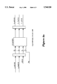
- FIG. 2 An alternate scheme that is more complex and requires more hardware is illustrated in FIG. 2.
- This alternate scheme utilizes a FIFO to accommodate address and data information, command and byte enable information and select information. It divides the bursts into single transactions, which must be stored in a deep FIFO, such as a 10 entry and 40-bit wide FIFO as shown.
- a deep FIFO such as a 10 entry and 40-bit wide FIFO as shown.
- this approach is also inefficient because it is limited to the transfer of single transactions.
- it is also inefficient because for every transaction, an address must be followed by the associated data, resulting in inefficient use of the FIFO.
- a transaction queue for transferring data between a host bus and an internal system bus within a graphics controller comprises a First In First Out (FIFO) memory having independent clocks for reading and writing.
- the queue accommodates address information, data, command information, byte enable information, decode information, and a tag.
- the tag is a 2 bit field used to identify the queued entries as address, last data, and burst data.
- single transactions are written to the queue with no wait states.
- the address associated with the transaction is stored in the queue along with the command and decode information.
- a tag is also included that identifies the entry as an address.
- the data is stored in the next entry along with the byte enable information and a tag to indicate it is the last data of the transaction.
- the address entry is followed by multiple data entries that are each tagged as burst data. The final data entry of the burst will be tagged as the last data of the transaction in the same way as the data of a single transaction.
- FIG. 1 is a block diagram of a conventional transaction queue circuit.
- FIG. 2 is a block diagram of another conventional transaction queue circuit.
- FIG. 3 is a system block diagram illustrating an exemplary host interface circuit in a graphics controller utilizing a preferred embodiment of the Transaction Queue Circuit of the present invention.
- FIG. 4A is a block diagram illustrating the preferred embodiment of the Transaction Queue Circuit 12 of FIG. 3.
- FIG. 4B is a table of exemplary values stored in FIFO 18 of FIG. 4A for several transactions, illustrating the operation of the Transaction Queue Circuit 12 of FIG. 4A.
- FIG. 3 is a system block diagram illustrating an exemplary host interface circuit 10 within a graphics controller which utilizes a preferred embodiment of the Transaction Queue Circuit 12 of the present invention.
- the host interface circuit 10 is implemented around two internal busses: an internal host bus and an internal memory bus.
- the internal host bus is connected to an external host bus through a host interface module and the internal memory bus is connected to a Random Access Memory bus ("Rambus") channel through a Rambus Interface Access Channel.
- the internal memory bus is also accessible by modules external to the host interface circuit 10 such as a video graphics adapter module or a direct frame buffer module.
- the host interface circuit 10 synchronizes the host clock, which in the present example is a 33 MHz clock signal, to the internal system clock, which in the present case is a 62.5 MHz clock signal.
- the Transaction Queue Circuit 12 comprises a First In First Out (FIFO) buffer 18 which receives data via an Address/Data Register 16 and provides data to an Output Register 34.
- the Transaction Queue Circuit 12 is also coupled to the host and the internal system clocks for writing and reading, respectively.
- the FIFO 18 is 8 entries deep by 42 bits wide.
- a PCI Controller 30 writes to the FIFO 18 on the rising edge of the host clock.
- the FIFO 18 is read by an Internal Bus Controller 36 on the rising edge of the internal system clock.
- the Transaction Queue Circuit 12 accommodates address information and data 20, command and byte enable information 21, select information 22 and a tag value 23.
- the tag value 23 is provided in a 2 bit field used to identify the queued entries as either an address, the last data or burst data, as will be described in detail below.
- the FIFO 18 provides the temporary storage required to allow both busses to effectively run with zero wait states. For example, though the internal host bus can transfer data almost twice as fast as the PCI bus, the Transaction Queue Circuit 12 provides the temporary storage for the host PCI data that gets transferred before the internal host bus burst actually begins. As a result, transactions between the two busses can be provided without any waiting.
- the Transaction Queue Circuit 12 also synchronizes write cycles between the two clock domains. Host accesses to registers internal to the host interface circuit 10 on the graphics controller do not go through the Transaction Queue Circuit 12 and can occur concurrently with queued graphics controller resource accesses.
- the Transaction Queue Circuit 12 allows host write transactions, including multiple data phase bursts, to occur at full speed on the external host bus, while providing transaction information to the graphics controller resources on the internal host bus running at the system clock rate. Information read from the FIFO 18 of the Transaction Queue Circuit 12 is passed to an Output Register 34, where data is held during the internal host bus transaction.
- Multiplexed address and data 20 are provided via the external host bus to signal line 14, registered with Address/Data Register 16 and then connected to 32 bits of the FIFO 18.
- Multiplexed command and byte enable information 21 provided via the external host bus to signal line 24, registered with Address/Data Register 16 and then connected to 4 bits of the FIFO 18.
- the select information 22 originates from an Address/Command Decoder 26, which also receives the multiplexed address and data via signal line 14, as well as the multiplexed command and byte enable information provided on signal line 24.
- the output of the Decoder 26 is registered with Address/Data Register 16 and then connected to 4 bits of the FIFO 18.
- Control data is provided via the external host bus to signal line 28, which in turn provides the control data to PCI Controller 30.
- the PCI Controller 30 also receives a signal from Decoder 26 which indicates whether the data the Decoder 26 received on signal lines 14 and 24 are valid. In addition, the PCI Controller 30 receives the same clock signal as used by the external host bus, which in the present example is a 33 MHz clock signal. In response, the PCI Controller 30 generates a tag value 23 via signal line 32 according to whether it is currently loading an address (11b binary!), burst data (00b binary!), or last data (10b binary!), as will be discussed in detail in the following sections. Signal line 32 is connected to 2 bits of the FIFO 18.
- the Output Register 34 receives address information and data 20, command and byte enable information 21 and select information 22 from the FIFO 18. This information 20-22 is held in the Output Register 34 and driven onto the internal host bus during transactions.
- the Output Register 34 has 36 bits for address information and data 20, 4 bits for the command and byte enable information 21, and 4 bits for the select information 22.
- FIG. 4A is a block diagram illustrating the preferred embodiment of the Transaction Queue Circuit 12 of the present invention.
- FIG. 4B is a table illustrating examples of several transactions.
- Information 20-22 is read from the Transaction Queue Circuit 12 as controlled by the Internal Bus Controller 36 via signal line 38 when an empty flag ("EF") is deasserted.
- the multiplexed address and data 20, multiplexed command and byte enable information 21 and select information 22 are provided to Output Register 34 and the tag value 23 is provided to the Internal Bus Controller 36.
- the Internal Bus Controller 36 uses the tag value 23 to determine the type of information read. As shown in FIG. 4B, the first entry (0) is read and found to contain address (A1.1), command (C1.1), select (S1.1), and a tag value of 11b. The Internal Bus Controller 36 identifies this as address phase information and will store it in the Output Register 34. The next entry (1) will be read from the FIFO 18 and the tag value 23 will be examined. In this example, the tag value 23 is 10b, which signifies the last data of the transaction. The Internal Bus Controller 36 will begin a single transaction on the internal bus using the address (A1.1), command (C1.1), and select (S1.1) previously stored in the Output Register 34.
- the data (D1.1) and byte enable information 21 (B1.1) from the FIFO 18 will be loaded into the Output Register 34 on the next clock to be used during the data phase. This would complete the first transaction, and the Internal Bus Controller 36 would then continue by reading the next entry of the FIFO 18.
- the next entry (2) contains a new address (A2.1), command (C2.1), select (S2.1) and an address tag (11b).
- the information will be again stored in the Output Register 34 while the next entry (3) is read.
- Entry 3 contains a tag value 23 of 00b which indicates it contains burst data (D2.1) and corresponding byte enable information (B2.1).
- the Internal Bus Controller 36 will begin a burst transaction using the previously stored address (A2.1), command (C2.1), select (S2.1) information obtained during the address phase.
- the data (D2.1) and byte enable information 21 (B2.1) will be used on the next clock for the data phase, and the Internal Bus Controller 36 will read the next entry (4) from the FIFO 18.
- the tag value 23 of 00b indicates there is more burst data (D2.2) and byte enable information (B2.2), which will be loaded into the Output Register 34 and the burst transaction will continue.
- the next entry (5) is read and the tag value 23 of 10b indicates that this is the last data of the transaction.
- the data (D2.3) and byte enable information 21 (B2.3) will be used during the final data phase and the burst transaction is complete.
- the final two entries indicate a single transaction which will be processed by the Internal Bus Controller 36 in the same way as described above.
- the present invention provides an efficient use of hardware because it accommodates multiplexed information directly from the PCI bus.
- the present invention which utilizes a tagged scheme, is advantageous over non-tagged schemes such as that shown in FIGS. 1 and 2 as it requires fewer FIFO bits, less complex control logic, and works well with the multiplexed PCI bus.
- the present invention facilitates the operation of the processor at optimal speed.
- the combination of address and data tags as provided by the present invention also allows data transactions to be generated on the internal bus in a burst or non-burst manner, depending on the corresponding PCI transaction.
Abstract
Description
Claims (20)
Priority Applications (1)
| Application Number | Priority Date | Filing Date | Title |
|---|---|---|---|
| US08/536,689 US5748920A (en) | 1995-06-23 | 1995-09-29 | Transaction queue in a graphics controller chip |
Applications Claiming Priority (2)
| Application Number | Priority Date | Filing Date | Title |
|---|---|---|---|
| US49295P | 1995-06-23 | 1995-06-23 | |
| US08/536,689 US5748920A (en) | 1995-06-23 | 1995-09-29 | Transaction queue in a graphics controller chip |
Publications (1)
| Publication Number | Publication Date |
|---|---|
| US5748920A true US5748920A (en) | 1998-05-05 |
Family
ID=26667719
Family Applications (1)
| Application Number | Title | Priority Date | Filing Date |
|---|---|---|---|
| US08/536,689 Expired - Lifetime US5748920A (en) | 1995-06-23 | 1995-09-29 | Transaction queue in a graphics controller chip |
Country Status (1)
| Country | Link |
|---|---|
| US (1) | US5748920A (en) |
Cited By (7)
| Publication number | Priority date | Publication date | Assignee | Title |
|---|---|---|---|---|
| US6286074B1 (en) | 1999-03-24 | 2001-09-04 | International Business Machines Corporation | Method and system for reading prefetched data across a bridge system |
| US6425023B1 (en) | 1999-03-24 | 2002-07-23 | International Business Machines Corporation | Method and system for gathering and buffering sequential data for a transaction comprising multiple data access requests |
| US6449678B1 (en) | 1999-03-24 | 2002-09-10 | International Business Machines Corporation | Method and system for multiple read/write transactions across a bridge system |
| US6481251B1 (en) * | 1999-10-25 | 2002-11-19 | Advanced Micro Devices, Inc. | Store queue number assignment and tracking |
| US6502157B1 (en) | 1999-03-24 | 2002-12-31 | International Business Machines Corporation | Method and system for perfetching data in a bridge system |
| US6523109B1 (en) | 1999-10-25 | 2003-02-18 | Advanced Micro Devices, Inc. | Store queue multimatch detection |
| US20040056865A1 (en) * | 1996-09-30 | 2004-03-25 | Tetsuya Shimomura | Data processor having unified memory architecture using register to optimize memory access |
Citations (5)
| Publication number | Priority date | Publication date | Assignee | Title |
|---|---|---|---|---|
| US5469544A (en) * | 1992-11-09 | 1995-11-21 | Intel Corporation | Central processing unit address pipelining |
| US5469558A (en) * | 1991-08-16 | 1995-11-21 | Multichip Technology | Dynamically reconfigurable memory system with programmable controller and FIFO buffered data channels |
| US5471637A (en) * | 1988-12-30 | 1995-11-28 | Intel Corporation | Method and apparatus for conducting bus transactions between two clock independent bus agents of a computer system using a transaction by transaction deterministic request/response protocol and burst transfer |
| US5499385A (en) * | 1990-04-18 | 1996-03-12 | Rambus, Inc. | Method for accessing and transmitting data to/from a memory in packets |
| US5553262A (en) * | 1988-01-21 | 1996-09-03 | Mitsubishi Denki Kabushiki Kaisha | Memory apparatus and method capable of setting attribute of information to be cached |
-
1995
- 1995-09-29 US US08/536,689 patent/US5748920A/en not_active Expired - Lifetime
Patent Citations (6)
| Publication number | Priority date | Publication date | Assignee | Title |
|---|---|---|---|---|
| US5553262A (en) * | 1988-01-21 | 1996-09-03 | Mitsubishi Denki Kabushiki Kaisha | Memory apparatus and method capable of setting attribute of information to be cached |
| US5553262B1 (en) * | 1988-01-21 | 1999-07-06 | Mitsubishi Electric Corp | Memory apparatus and method capable of setting attribute of information to be cached |
| US5471637A (en) * | 1988-12-30 | 1995-11-28 | Intel Corporation | Method and apparatus for conducting bus transactions between two clock independent bus agents of a computer system using a transaction by transaction deterministic request/response protocol and burst transfer |
| US5499385A (en) * | 1990-04-18 | 1996-03-12 | Rambus, Inc. | Method for accessing and transmitting data to/from a memory in packets |
| US5469558A (en) * | 1991-08-16 | 1995-11-21 | Multichip Technology | Dynamically reconfigurable memory system with programmable controller and FIFO buffered data channels |
| US5469544A (en) * | 1992-11-09 | 1995-11-21 | Intel Corporation | Central processing unit address pipelining |
Cited By (11)
| Publication number | Priority date | Publication date | Assignee | Title |
|---|---|---|---|---|
| US20040056865A1 (en) * | 1996-09-30 | 2004-03-25 | Tetsuya Shimomura | Data processor having unified memory architecture using register to optimize memory access |
| US6717583B2 (en) * | 1996-09-30 | 2004-04-06 | Hitachi, Ltd. | Data processor having unified memory architecture providing priority memory access |
| US6954206B2 (en) | 1996-09-30 | 2005-10-11 | Hitachi, Ltd. | Data processor having unified memory architecture using register to optimize memory access |
| US20050264574A1 (en) * | 1996-09-30 | 2005-12-01 | Tetsuya Shimomura | Data processor having unified memory architecture using register to optimize memory access |
| US7333116B2 (en) | 1996-09-30 | 2008-02-19 | Renesas Technology Corporation | Data processor having unified memory architecture using register to optimize memory access |
| US6286074B1 (en) | 1999-03-24 | 2001-09-04 | International Business Machines Corporation | Method and system for reading prefetched data across a bridge system |
| US6425023B1 (en) | 1999-03-24 | 2002-07-23 | International Business Machines Corporation | Method and system for gathering and buffering sequential data for a transaction comprising multiple data access requests |
| US6449678B1 (en) | 1999-03-24 | 2002-09-10 | International Business Machines Corporation | Method and system for multiple read/write transactions across a bridge system |
| US6502157B1 (en) | 1999-03-24 | 2002-12-31 | International Business Machines Corporation | Method and system for perfetching data in a bridge system |
| US6481251B1 (en) * | 1999-10-25 | 2002-11-19 | Advanced Micro Devices, Inc. | Store queue number assignment and tracking |
| US6523109B1 (en) | 1999-10-25 | 2003-02-18 | Advanced Micro Devices, Inc. | Store queue multimatch detection |
Similar Documents
| Publication | Publication Date | Title |
|---|---|---|
| US5978866A (en) | Distributed pre-fetch buffer for multiple DMA channel device | |
| US6115761A (en) | First-In-First-Out (FIFO) memories having dual descriptors and credit passing for efficient access in a multi-processor system environment | |
| US5568619A (en) | Method and apparatus for configuring a bus-to-bus bridge | |
| US6131127A (en) | I/O transactions on a low pin count bus | |
| US6480198B2 (en) | Multi-function controller and method for a computer graphics display system | |
| US5649230A (en) | System for transferring data using value in hardware FIFO'S unused data start pointer to update virtual FIFO'S start address pointer for fast context switching | |
| US5673396A (en) | Adjustable depth/width FIFO buffer for variable width data transfers | |
| US5857084A (en) | Hierarchical bus structure access system | |
| US4860244A (en) | Buffer system for input/output portion of digital data processing system | |
| US6157970A (en) | Direct memory access system using time-multiplexing for transferring address, data, and control and a separate control line for serially transmitting encoded DMA channel number | |
| US6636927B1 (en) | Bridge device for transferring data using master-specific prefetch sizes | |
| US6173353B1 (en) | Method and apparatus for dual bus memory transactions | |
| US7251188B2 (en) | Memory access interface for a micro-controller system with address/data multiplexing bus | |
| US6510497B1 (en) | Method and system for page-state sensitive memory control and access in data processing systems | |
| US5014236A (en) | Input/output bus expansion interface | |
| US6160562A (en) | System and method for aligning an initial cache line of data read from local memory by an input/output device | |
| US6381672B1 (en) | Speculative opening of a new page when approaching page boundary during read/write of isochronous streams | |
| US5416916A (en) | Structure for enabling direct memory-to-memory transfer with a fly-by DMA unit | |
| US6532019B1 (en) | Input/output integrated circuit hub incorporating a RAMDAC | |
| US5903776A (en) | Multiple priority accelerated graphics port (AGP) request queue | |
| US6615296B2 (en) | Efficient implementation of first-in-first-out memories for multi-processor systems | |
| US6782435B2 (en) | Device for spatially and temporally reordering for data between a processor, memory and peripherals | |
| US5748920A (en) | Transaction queue in a graphics controller chip | |
| US5983299A (en) | Priority request and bypass bus | |
| US5146572A (en) | Multiple data format interface |
Legal Events
| Date | Code | Title | Description |
|---|---|---|---|
| AS | Assignment |
Owner name: BANK OF AMERICA NATIONAL TRUST & SAVINGS ASSOCIATI Free format text: SECURITY AGREEMENT;ASSIGNOR:CIRRUS LOGIC, INC.;REEL/FRAME:008113/0001 Effective date: 19960430 |
|
| STCF | Information on status: patent grant |
Free format text: PATENTED CASE |
|
| FEPP | Fee payment procedure |
Free format text: PAYOR NUMBER ASSIGNED (ORIGINAL EVENT CODE: ASPN); ENTITY STATUS OF PATENT OWNER: LARGE ENTITY |
|
| FPAY | Fee payment |
Year of fee payment: 4 |
|
| REMI | Maintenance fee reminder mailed | ||
| AS | Assignment |
Owner name: NVIDIA INTERNATIONAL, INC., BARBADOS Free format text: ASSIGNMENT OF ASSIGNORS INTEREST;ASSIGNOR:CIRRUS LOGIC, INC.;REEL/FRAME:014646/0167 Effective date: 20030813 Owner name: NVIDIA INTERNATIONAL, INC. C/0 PRICEWATERHOUSECOOP Free format text: ASSIGNMENT OF ASSIGNORS INTEREST;ASSIGNOR:CIRRUS LOGIC, INC.;REEL/FRAME:014646/0167 Effective date: 20030813 |
|
| FPAY | Fee payment |
Year of fee payment: 8 |
|
| FPAY | Fee payment |
Year of fee payment: 12 |
|
| AS | Assignment |
Owner name: CIRRUS LOGIC, INC., TEXAS Free format text: DEED OF DISCHARGE;ASSIGNOR:BANK OF AMERICA NATIONAL TRUST & SAVINGS ASSOCIATION;REEL/FRAME:029353/0747 Effective date: 20040108 |
|
| AS | Assignment |
Owner name: NVIDIA CORPORATION, CALIFORNIA Free format text: ASSIGNMENT OF ASSIGNORS INTEREST;ASSIGNOR:NVIDIA INTERNATIONAL INC.;REEL/FRAME:029418/0249 Effective date: 20121203 |