US5663018A - Pattern writing method during X-ray mask fabrication - Google Patents
Pattern writing method during X-ray mask fabrication Download PDFInfo
- Publication number
- US5663018A US5663018A US08/654,457 US65445796A US5663018A US 5663018 A US5663018 A US 5663018A US 65445796 A US65445796 A US 65445796A US 5663018 A US5663018 A US 5663018A
- Authority
- US
- United States
- Prior art keywords
- layer
- pattern
- radiation
- exposing
- membrane
- Prior art date
- Legal status (The legal status is an assumption and is not a legal conclusion. Google has not performed a legal analysis and makes no representation as to the accuracy of the status listed.)
- Expired - Fee Related
Links
- 238000000034 method Methods 0.000 title claims abstract description 73
- 238000004519 manufacturing process Methods 0.000 title claims abstract description 26
- 239000012528 membrane Substances 0.000 claims abstract description 71
- 239000000463 material Substances 0.000 claims abstract description 65
- 230000005855 radiation Effects 0.000 claims abstract description 33
- 239000011358 absorbing material Substances 0.000 claims abstract description 18
- 229920002120 photoresistant polymer Polymers 0.000 claims description 11
- 238000010894 electron beam technology Methods 0.000 claims description 7
- 238000005530 etching Methods 0.000 claims description 3
- 239000010410 layer Substances 0.000 description 52
- XUIMIQQOPSSXEZ-UHFFFAOYSA-N Silicon Chemical compound [Si] XUIMIQQOPSSXEZ-UHFFFAOYSA-N 0.000 description 7
- 229910052710 silicon Inorganic materials 0.000 description 7
- 239000010703 silicon Substances 0.000 description 7
- 238000000059 patterning Methods 0.000 description 6
- 238000012545 processing Methods 0.000 description 6
- 238000007747 plating Methods 0.000 description 5
- 239000004065 semiconductor Substances 0.000 description 5
- 230000015572 biosynthetic process Effects 0.000 description 4
- 238000012986 modification Methods 0.000 description 4
- 230000004048 modification Effects 0.000 description 4
- 229910052581 Si3N4 Inorganic materials 0.000 description 3
- 239000011651 chromium Substances 0.000 description 3
- 239000010931 gold Substances 0.000 description 3
- VYZAMTAEIAYCRO-UHFFFAOYSA-N Chromium Chemical compound [Cr] VYZAMTAEIAYCRO-UHFFFAOYSA-N 0.000 description 2
- 239000006096 absorbing agent Substances 0.000 description 2
- WYTGDNHDOZPMIW-RCBQFDQVSA-N alstonine Natural products C1=CC2=C3C=CC=CC3=NC2=C2N1C[C@H]1[C@H](C)OC=C(C(=O)OC)[C@H]1C2 WYTGDNHDOZPMIW-RCBQFDQVSA-N 0.000 description 2
- 229910052804 chromium Inorganic materials 0.000 description 2
- 230000007423 decrease Effects 0.000 description 2
- 230000008021 deposition Effects 0.000 description 2
- PCHJSUWPFVWCPO-UHFFFAOYSA-N gold Chemical compound [Au] PCHJSUWPFVWCPO-UHFFFAOYSA-N 0.000 description 2
- 229910052737 gold Inorganic materials 0.000 description 2
- 229910001385 heavy metal Inorganic materials 0.000 description 2
- 150000002500 ions Chemical class 0.000 description 2
- 229920003229 poly(methyl methacrylate) Polymers 0.000 description 2
- 239000004926 polymethyl methacrylate Substances 0.000 description 2
- HQVNEWCFYHHQES-UHFFFAOYSA-N silicon nitride Chemical compound N12[Si]34N5[Si]62N3[Si]51N64 HQVNEWCFYHHQES-UHFFFAOYSA-N 0.000 description 2
- 239000000956 alloy Substances 0.000 description 1
- 229910045601 alloy Inorganic materials 0.000 description 1
- 238000013459 approach Methods 0.000 description 1
- XTDAIYZKROTZLD-UHFFFAOYSA-N boranylidynetantalum Chemical compound [Ta]#B XTDAIYZKROTZLD-UHFFFAOYSA-N 0.000 description 1
- 239000013590 bulk material Substances 0.000 description 1
- 238000006073 displacement reaction Methods 0.000 description 1
- 230000000694 effects Effects 0.000 description 1
- 125000001183 hydrocarbyl group Chemical group 0.000 description 1
- 230000009191 jumping Effects 0.000 description 1
- 239000002245 particle Substances 0.000 description 1
- HBMJWWWQQXIZIP-UHFFFAOYSA-N silicon carbide Chemical compound [Si+]#[C-] HBMJWWWQQXIZIP-UHFFFAOYSA-N 0.000 description 1
- HWEYZGSCHQNNEH-UHFFFAOYSA-N silicon tantalum Chemical compound [Si].[Ta] HWEYZGSCHQNNEH-UHFFFAOYSA-N 0.000 description 1
- 239000002356 single layer Substances 0.000 description 1
- 238000012546 transfer Methods 0.000 description 1
Images


Classifications
-
- G—PHYSICS
- G03—PHOTOGRAPHY; CINEMATOGRAPHY; ANALOGOUS TECHNIQUES USING WAVES OTHER THAN OPTICAL WAVES; ELECTROGRAPHY; HOLOGRAPHY
- G03F—PHOTOMECHANICAL PRODUCTION OF TEXTURED OR PATTERNED SURFACES, e.g. FOR PRINTING, FOR PROCESSING OF SEMICONDUCTOR DEVICES; MATERIALS THEREFOR; ORIGINALS THEREFOR; APPARATUS SPECIALLY ADAPTED THEREFOR
- G03F1/00—Originals for photomechanical production of textured or patterned surfaces, e.g., masks, photo-masks, reticles; Mask blanks or pellicles therefor; Containers specially adapted therefor; Preparation thereof
- G03F1/22—Masks or mask blanks for imaging by radiation of 100nm or shorter wavelength, e.g. X-ray masks, extreme ultraviolet [EUV] masks; Preparation thereof
-
- G—PHYSICS
- G03—PHOTOGRAPHY; CINEMATOGRAPHY; ANALOGOUS TECHNIQUES USING WAVES OTHER THAN OPTICAL WAVES; ELECTROGRAPHY; HOLOGRAPHY
- G03F—PHOTOMECHANICAL PRODUCTION OF TEXTURED OR PATTERNED SURFACES, e.g. FOR PRINTING, FOR PROCESSING OF SEMICONDUCTOR DEVICES; MATERIALS THEREFOR; ORIGINALS THEREFOR; APPARATUS SPECIALLY ADAPTED THEREFOR
- G03F7/00—Photomechanical, e.g. photolithographic, production of textured or patterned surfaces, e.g. printing surfaces; Materials therefor, e.g. comprising photoresists; Apparatus specially adapted therefor
- G03F7/70—Microphotolithographic exposure; Apparatus therefor
- G03F7/70425—Imaging strategies, e.g. for increasing throughput or resolution, printing product fields larger than the image field or compensating lithography- or non-lithography errors, e.g. proximity correction, mix-and-match, stitching or double patterning
-
- G—PHYSICS
- G03—PHOTOGRAPHY; CINEMATOGRAPHY; ANALOGOUS TECHNIQUES USING WAVES OTHER THAN OPTICAL WAVES; ELECTROGRAPHY; HOLOGRAPHY
- G03F—PHOTOMECHANICAL PRODUCTION OF TEXTURED OR PATTERNED SURFACES, e.g. FOR PRINTING, FOR PROCESSING OF SEMICONDUCTOR DEVICES; MATERIALS THEREFOR; ORIGINALS THEREFOR; APPARATUS SPECIALLY ADAPTED THEREFOR
- G03F7/00—Photomechanical, e.g. photolithographic, production of textured or patterned surfaces, e.g. printing surfaces; Materials therefor, e.g. comprising photoresists; Apparatus specially adapted therefor
- G03F7/70—Microphotolithographic exposure; Apparatus therefor
- G03F7/70691—Handling of masks or workpieces
- G03F7/70783—Handling stress or warp of chucks, masks or workpieces, e.g. to compensate for imaging errors or considerations related to warpage of masks or workpieces due to their own weight
-
- G—PHYSICS
- G03—PHOTOGRAPHY; CINEMATOGRAPHY; ANALOGOUS TECHNIQUES USING WAVES OTHER THAN OPTICAL WAVES; ELECTROGRAPHY; HOLOGRAPHY
- G03F—PHOTOMECHANICAL PRODUCTION OF TEXTURED OR PATTERNED SURFACES, e.g. FOR PRINTING, FOR PROCESSING OF SEMICONDUCTOR DEVICES; MATERIALS THEREFOR; ORIGINALS THEREFOR; APPARATUS SPECIALLY ADAPTED THEREFOR
- G03F7/00—Photomechanical, e.g. photolithographic, production of textured or patterned surfaces, e.g. printing surfaces; Materials therefor, e.g. comprising photoresists; Apparatus specially adapted therefor
- G03F7/70—Microphotolithographic exposure; Apparatus therefor
- G03F7/708—Construction of apparatus, e.g. environment aspects, hygiene aspects or materials
- G03F7/70858—Environment aspects, e.g. pressure of beam-path gas, temperature
- G03F7/70866—Environment aspects, e.g. pressure of beam-path gas, temperature of mask or workpiece
Definitions
- This invention pertains to X-ray mask fabrication and more specifically to methods of forming patterns in X-ray masks with less distortion.
- X-ray masks are formed on a semiconductor wafer, such as a silicon wafer.
- the silicon wafer operates like a frame and support for the mask.
- a thin membrane is deposited on the upper surface of the wafer in the form of a thin layer.
- a layer of X-ray absorbing material such as some safe heavy metal or alloy, is deposited on the upper surface of the membrane layer.
- the X-ray absorbing layer is patterned by applying a hard mask material and resist.
- the resist is patterned (or exposed) with an electron beam (E-beam) device and a hard mask is formed by etching the hard mask layer through the patterned photoresist layer.
- E-beam electron beam
- the hard mask is then used as an etch mask to pattern the X-ray absorbing layer.
- the wafer is etched from the membrane layer in a circle or a rectangle to form a thin membrane.
- the mask thus allows X-rays to pass through the thin membrane and portions of the X-ray absorbing layer that have been etched away.
- the entire procedure is known as a process flow and two different process flows are commonly used.
- the wafer flow In the first process flow, commonly referred to as a wafer flow, all processing is done on the wafer with one of the final steps being the back etching of the silicon wafer to form the membrane.
- the wafer flow was primarily created to solve formatting issues. It allows X-ray mask processing to be conducted in semiconductor tools that are not dramatically different from the standard wafer processing tools supplied by the industry.
- the X-ray mask specific processing steps (membrane formation and wafer mounting to a support ring) are at the end of the flow. This minimizes the modifications necessary to both the tools and the wafer processes.
- the creation of the membrane and the mounting of the wafer creates significant pattern displacement errors ( ⁇ 0.15 ⁇ m) in the mask.
- the second process flow is commonly referred to as a membrane flow.
- the membrane In the membrane flow the membrane is formed early in the process (generally after absorber deposition) and the remaining processing is carried out on the membrane.
- the membrane flow process was derived to remove the errors in the wafer flow process by conducting the mask specific processing steps before the absorber layer is patterned. While this greatly reduces the errors associated with membrane formation and wafer mounting, it also increases the modifications to both the equipment (the tools must accept an X-ray mask format rather than a wafer) and the processes (the patterning defining process steps are carried out on a membrane rather than a wafer).
- a pattern writing method for membrane structure fabrication including the steps of forming a membrane structure, and forming a material system on the membrane structure including the steps of providing a layer of material with internal stresses, the internal stresses being altered by exposure of the material to radiation to produce altered internal stresses in exposed areas, and exposing the layer of material to radiation to define a pattern, the exposing being performed in associated areas such that the internal stresses within the layer of material and altered internal stresses in the associated areas are substantially offset to reduce distortion in the material system and in the membrane structure.
- this method is used to fabricate X-ray masks with smaller errors, or less distortion, in a pattern.
- the method includes forming an etch mask on a layer of X-ray absorbing material including the steps of providing a layer of photoresist sensitive to an electron beam, the photoresist having internal stresses which are altered by exposure to the electron beam, and exposing the photoresist to the electron beam to define a pattern, the exposing being performed in associated areas such that the internal stresses within the photoresist and altered internal stresses in the associated areas are substantially offset to reduce distortion in the etch mask and in the layer of X-ray absorbing material.
- the radiation sensitive material is exposed to radiation to define the chosen pattern by exposing the layer of material in a spiral path starting at approximately a central portion of the layer of material. This produces a minimum amount of distortion while maintaining maximum patterning speed.
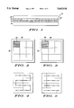
- FIG. 1 is a simplified sectional view illustrating various layers used in the fabrication of an X-ray mask
- FIG. 2 is a view in top plan of the structure of FIG. 1, illustrating cells of a pattern to be written;
- FIG. 3 is a view similar to FIG. 2 illustrating distortion in the structure due to the writing procedure
- FIGS. 4 and 5 illustrate prior art writing procedures which resulted in the distortion illustrated in FIG. 3;
- FIG. 6 illustrates magnification due to uniform stress relief over an entire patterned area
- FIG. 7 illustrates a writing procedure in accordance with the present invention.
- FIG. 8 is a distortion map illustrating resultant distortions due to the writing procedure illustrated in FIG. 7.
- FIG. 1 is a simplified sectional view of a step in a process of forming a refractory radiation mask 10 by membrane flow in accordance with the present invention.
- the radiation used for exemplary purposes is X-rays but it could also include light, electrons, ions, or other charged particles.
- Mask 10 includes a supporting member (not shown) which is referred to herein as a "wafer".
- the supporting member will be a semiconductor wafer, such as a silicon wafer.
- the wafer commonly used by today's manufacturers is a silicon wafer 76 mm in diameter and 2 mm thick.
- the term "wafer" is intended to encompass all such members.
- a membrane layer 12 is formed on a planar upper surface of the supporting member by any convenient method, including epitaxial growth, deposition, etc.
- membrane layer 12 is formed of some convenient material, such as silicon (Si), silicon nitride (SiN), or silicon carbide (SiC), or the like, and in this specific example is boron-doped silicon (B:Si).
- Si silicon
- SiN silicon nitride
- SiC silicon carbide
- B:Si boron-doped silicon
- membrane layer 12 is approximately 2,5 ⁇ m thick and has original stresses of approximately 5E8 dyne/cm 2 .
- the material used for membrane layer 12 does not have a significant effect on the resulting distortions.
- a bi-layer plating base including a layer 13 of chromium (Cr) and a layer 14 of gold (Au), is deposited on the surface of membrane layer 12 as an X-ray absorbing material.
- the X-ray absorbing material may be any convenient material which will absorb X-rays passing through membrane layer 12 so as to prevent the X-rays from passing on through layer 13. Materials such as tantalum-silicon nitride (TaSiN), tantalum-boride (Ta 4 B), heavy metals, etc. are commonly used.
- chromium layer 13 is approximately 0.005 ⁇ m thick and gold layer 14 is approximately 0.03 ⁇ m thick.
- the bi-layer plating base has original stresses of approximately 3E8 dyne/cm 2 . The stress of the bi-layer plating base is normally measured as a stack so that only one value is provided.
- the present fabrication technique generally applies to the membrane flow, a portion of the wafer is removed at this time (prior to the formation of an etch mask 15), thereby essentially forming membrane layer 12 into a membrane.
- the membrane may have substantially any desired configuration but in a preferred embodiment will be rectangular. While the present novel method is most applicable to the wafer flow, it will be understood that in some special applications it may also be applicable to the membrane flow, or to any modified types of flow.
- etch mask 15 is formed on the upper surface of layer 14 for the purpose of transferring a chosen pattern to layers 13 and 14, as will be explained in more detail below.
- at least one layer of etch mask 15 is formed of material which is sensitive to radiation of some type, e.g. electron beams, light, etc.
- etch mask 15 may be formed using a wide variety of methods and materials or layers of materials, all well known in the art, in this embodiment etch mask 15 includes a single layer of photoresist layer 20 which is being used for purposes of simplifying this explanation.
- Layer 20 is formed of polymethylmethacrylate (PMMA) on which can easily be written the chosen pattern, for example with an electron beam (E-beam) device or the like.
- PMMA polymethylmethacrylate
- the bi-layer plating base is etched to transfer the pattern thereto, using photoresist layer 20 as a mask.
- Etch mask 15 is removable so that once the chosen pattern has been transferred to the bi-layer plating base etch mask 15 can be easily removed.
- FIG. 2 is a view in top plan of the structure of FIG. 1, illustrating cells of a pattern to be written and FIG. 3 is a view similar to FIG. 2 illustrating distortion in the structure due to the writing procedure.
- FIG. 3 illustrates the manner in which the membrane/resist distorts after cell has been written or exposed.
- the E-beam writing decreases the stress in cell 25 and thus cell 25 expands until its stress is again in equilibrium with the surrounding material. This is quite undesirable because the E-beam device will Write a second cell 27 as though the membrane/resist were still undistorted.
- the pattern will continue to be written on a distorted membrane/resist system and the membrane/resist system will continue to distort further as subsequent cells are written.
- the final pattern produced will not match the pattern programmed into the E-beam device.
- E-beam devices generally have the flexibility to write the pattern cells in any order
- two methods are used extensively. These methods are the serpentine method illustrated in FIG. 4 and the unidirectional method illustrated in FIG. 5. In both figures, the arrows illustrate the direction of movement of the E-beam device.
- the serpentine style is the fastest writing approach since all cells are written consecutively.
- the unidirectional style writing method each row is written in the same direction and then the E-beam repositions to the beginning of the next row. Both of these writing methods produce the pattern distortion explained above.
- FIG. 7 a novel pattern writing sequence is illustrated which substantially counteracts the simple magnification of FIG. 6 while still maintaining maximum patterning speed.
- a first cell to be written designated 30, borders the pattern center rather than a corner of the area to be exposed.
- the next three cells, designated 31, 32, and 33, respectively, patterned, complete an exposed square region at the center of the membrane area. This stress-relieved center square causes all unwritten cells to displace radially, similar to the magnification error illustrated in FIG. 6.
- the patterned area contracts toward the center of the membrane area, counteracting the magnification displayed in FIG. 6.
- the exposing is performed in associated areas such that the internal or original stresses within layer 20 and altered internal stresses (altered by the writing process) in the associated areas are substantially offset to reduce distortion in the material system and in the membrane structure.
- a distortion map is provided in FIG. 8, which map illustrates the distortion resulting from the novel patterning procedure. This map illustrates that the maximum distortion vector has been reduced over 50% to 17.8 nm.
- a writing procedure utilizing a spiral starting at approximately a central portion of the layer of radiation sensitive material (or the membrane area) is disclosed as a preferred embodiment, it should be noted that other writing procedures might be utilized which expose associated areas such that the internal or original stresses within layer 20 and altered internal stresses (altered by the writing process) in the associated areas are substantially offset to reduce distortion in the material system and in the membrane structure. Examples of other writing procedures are: a spiral path starting at an outer edge; discontinuously jumping to associated or offsetting cells or areas; etc. It should also be noted that the present writing system can be used in multi-pass writing techniques, the simplest example of which is a two-pass exposure in which each cell is only exposed 50% of the required exposure on each pass. In multi-pass writing techniques, the same or different paths might be used for each pass.
- new and improved methods of fabricating X-ray masks have been disclosed, which methods compensate for distortion during pattern writing so as to greatly improve the accuracy.
- new and improved methods of fabricating X-ray masks including the use of a new pattern writing technique which substantially reduces distortion during fabrication of the X-ray mask have been disclosed.
- the new technique not only substantially reduces distortion in the pattern caused by writing radiation sensitive material but also, in the preferred embodiment, maintains maximum patterning speed.
Abstract
Description
Claims (16)
Priority Applications (2)
| Application Number | Priority Date | Filing Date | Title |
|---|---|---|---|
| US08/654,457 US5663018A (en) | 1996-05-28 | 1996-05-28 | Pattern writing method during X-ray mask fabrication |
| JP15297197A JPH1070074A (en) | 1996-05-28 | 1997-05-27 | Pattern writing method in the course of manufacturing x-ray mask |
Applications Claiming Priority (1)
| Application Number | Priority Date | Filing Date | Title |
|---|---|---|---|
| US08/654,457 US5663018A (en) | 1996-05-28 | 1996-05-28 | Pattern writing method during X-ray mask fabrication |
Publications (1)
| Publication Number | Publication Date |
|---|---|
| US5663018A true US5663018A (en) | 1997-09-02 |
Family
ID=24624941
Family Applications (1)
| Application Number | Title | Priority Date | Filing Date |
|---|---|---|---|
| US08/654,457 Expired - Fee Related US5663018A (en) | 1996-05-28 | 1996-05-28 | Pattern writing method during X-ray mask fabrication |
Country Status (2)
| Country | Link |
|---|---|
| US (1) | US5663018A (en) |
| JP (1) | JPH1070074A (en) |
Cited By (71)
| Publication number | Priority date | Publication date | Assignee | Title |
|---|---|---|---|---|
| US20010037387A1 (en) * | 2000-03-21 | 2001-11-01 | F5 Networks, Inc., | Method and system for optimizing a network by independently scaling control segments and data flow |
| US20010047415A1 (en) * | 2000-01-31 | 2001-11-29 | Skene Bryan D. | Method and system for enabling persistent access to virtual servers by an ldns server |
| US20010052016A1 (en) * | 1999-12-13 | 2001-12-13 | Skene Bryan D. | Method and system for balancing load distrubution on a wide area network |
| US6405219B2 (en) | 1999-06-22 | 2002-06-11 | F5 Networks, Inc. | Method and system for automatically updating the version of a set of files stored on content servers |
| US20020138618A1 (en) * | 2000-03-21 | 2002-09-26 | F5 Networks, Inc. | Simplified method for processing multiple connections from the same client |
| US6473802B2 (en) | 1999-07-15 | 2002-10-29 | F5 Networks, Inc. | Method and system for storing load balancing information with an HTTP cookie |
| US20060158088A1 (en) * | 2005-01-05 | 2006-07-20 | Samsung Sdi Co., Ltd. | Method of forming shadow mask pattern |
| US7146354B1 (en) | 1999-06-18 | 2006-12-05 | F5 Networks, Inc. | Method and system for network load balancing with a compound data structure |
| US7287084B1 (en) | 1999-07-15 | 2007-10-23 | F5 Networks, Inc. | Enabling encryption of application level persistence between a server and a client |
| US20070276120A1 (en) * | 2006-05-24 | 2007-11-29 | Debruin Bruce Roger | Crystallizer temperature control via fluid control |
| US7346695B1 (en) | 2002-10-28 | 2008-03-18 | F5 Networks, Inc. | System and method for performing application level persistence |
| CN1800970B (en) * | 2005-01-05 | 2011-02-09 | 三星移动显示器株式会社 | Forming method of mask pattern |
| US7975025B1 (en) | 2008-07-08 | 2011-07-05 | F5 Networks, Inc. | Smart prefetching of data over a network |
| US7996886B1 (en) | 2002-09-03 | 2011-08-09 | F5 Networks, Inc. | Method and system for providing persistence in a secure network access |
| US8463909B1 (en) | 2010-09-15 | 2013-06-11 | F5 Networks, Inc. | Systems and methods for managing server resources |
| US8566444B1 (en) | 2008-10-30 | 2013-10-22 | F5 Networks, Inc. | Methods and system for simultaneous multiple rules checking |
| US8566452B1 (en) | 2006-08-03 | 2013-10-22 | F5 Networks, Inc. | Intelligent HTTP based load-balancing, persistence, and application traffic management of SSL VPN tunnels |
| US8627467B2 (en) | 2011-01-14 | 2014-01-07 | F5 Networks, Inc. | System and method for selectively storing web objects in a cache memory based on policy decisions |
| US8630174B1 (en) | 2010-09-14 | 2014-01-14 | F5 Networks, Inc. | System and method for post shaping TCP packetization |
| US8806053B1 (en) | 2008-04-29 | 2014-08-12 | F5 Networks, Inc. | Methods and systems for optimizing network traffic using preemptive acknowledgment signals |
| US8804504B1 (en) | 2010-09-16 | 2014-08-12 | F5 Networks, Inc. | System and method for reducing CPU load in processing PPP packets on a SSL-VPN tunneling device |
| US8868961B1 (en) | 2009-11-06 | 2014-10-21 | F5 Networks, Inc. | Methods for acquiring hyper transport timing and devices thereof |
| US8886981B1 (en) | 2010-09-15 | 2014-11-11 | F5 Networks, Inc. | Systems and methods for idle driven scheduling |
| US8908545B1 (en) | 2010-07-08 | 2014-12-09 | F5 Networks, Inc. | System and method for handling TCP performance in network access with driver initiated application tunnel |
| US8959571B2 (en) | 2010-10-29 | 2015-02-17 | F5 Networks, Inc. | Automated policy builder |
| US9083760B1 (en) | 2010-08-09 | 2015-07-14 | F5 Networks, Inc. | Dynamic cloning and reservation of detached idle connections |
| US9141625B1 (en) | 2010-06-22 | 2015-09-22 | F5 Networks, Inc. | Methods for preserving flow state during virtual machine migration and devices thereof |
| US9154423B1 (en) | 2012-05-01 | 2015-10-06 | F5 Networks, Inc. | Minimize SYN-flood issues with flow cache while maintaining performance |
| US9172753B1 (en) | 2012-02-20 | 2015-10-27 | F5 Networks, Inc. | Methods for optimizing HTTP header based authentication and devices thereof |
| US9203771B1 (en) | 2012-07-23 | 2015-12-01 | F5 Networks, Inc. | Hot service flow hardware offloads based on service priority and resource usage |
| US9231879B1 (en) | 2012-02-20 | 2016-01-05 | F5 Networks, Inc. | Methods for policy-based network traffic queue management and devices thereof |
| US9246819B1 (en) | 2011-06-20 | 2016-01-26 | F5 Networks, Inc. | System and method for performing message-based load balancing |
| US9270766B2 (en) | 2011-12-30 | 2016-02-23 | F5 Networks, Inc. | Methods for identifying network traffic characteristics to correlate and manage one or more subsequent flows and devices thereof |
| US9313047B2 (en) | 2009-11-06 | 2016-04-12 | F5 Networks, Inc. | Handling high throughput and low latency network data packets in a traffic management device |
| US9338095B2 (en) | 2012-05-01 | 2016-05-10 | F5 Networks, Inc. | Data flow segment optimized for hot flows |
| US9525632B1 (en) | 2012-05-01 | 2016-12-20 | F5 Networks, Inc. | Minimize recycle SYN issues for split TCP hot flows to improve system reliability and performance |
| US9554276B2 (en) | 2010-10-29 | 2017-01-24 | F5 Networks, Inc. | System and method for on the fly protocol conversion in obtaining policy enforcement information |
| US10015286B1 (en) | 2010-06-23 | 2018-07-03 | F5 Networks, Inc. | System and method for proxying HTTP single sign on across network domains |
| US10015143B1 (en) | 2014-06-05 | 2018-07-03 | F5 Networks, Inc. | Methods for securing one or more license entitlement grants and devices thereof |
| USRE47019E1 (en) | 2010-07-14 | 2018-08-28 | F5 Networks, Inc. | Methods for DNSSEC proxying and deployment amelioration and systems thereof |
| US10097616B2 (en) | 2012-04-27 | 2018-10-09 | F5 Networks, Inc. | Methods for optimizing service of content requests and devices thereof |
| US10122630B1 (en) | 2014-08-15 | 2018-11-06 | F5 Networks, Inc. | Methods for network traffic presteering and devices thereof |
| US10135831B2 (en) | 2011-01-28 | 2018-11-20 | F5 Networks, Inc. | System and method for combining an access control system with a traffic management system |
| US10157280B2 (en) | 2009-09-23 | 2018-12-18 | F5 Networks, Inc. | System and method for identifying security breach attempts of a website |
| US10182013B1 (en) | 2014-12-01 | 2019-01-15 | F5 Networks, Inc. | Methods for managing progressive image delivery and devices thereof |
| US10187317B1 (en) | 2013-11-15 | 2019-01-22 | F5 Networks, Inc. | Methods for traffic rate control and devices thereof |
| US10230566B1 (en) | 2012-02-17 | 2019-03-12 | F5 Networks, Inc. | Methods for dynamically constructing a service principal name and devices thereof |
| US10375155B1 (en) | 2013-02-19 | 2019-08-06 | F5 Networks, Inc. | System and method for achieving hardware acceleration for asymmetric flow connections |
| US10404698B1 (en) | 2016-01-15 | 2019-09-03 | F5 Networks, Inc. | Methods for adaptive organization of web application access points in webtops and devices thereof |
| US10505792B1 (en) | 2016-11-02 | 2019-12-10 | F5 Networks, Inc. | Methods for facilitating network traffic analytics and devices thereof |
| US10505818B1 (en) | 2015-05-05 | 2019-12-10 | F5 Networks. Inc. | Methods for analyzing and load balancing based on server health and devices thereof |
| US10721269B1 (en) | 2009-11-06 | 2020-07-21 | F5 Networks, Inc. | Methods and system for returning requests with javascript for clients before passing a request to a server |
| US10791119B1 (en) | 2017-03-14 | 2020-09-29 | F5 Networks, Inc. | Methods for temporal password injection and devices thereof |
| US10791088B1 (en) | 2016-06-17 | 2020-09-29 | F5 Networks, Inc. | Methods for disaggregating subscribers via DHCP address translation and devices thereof |
| US10797888B1 (en) | 2016-01-20 | 2020-10-06 | F5 Networks, Inc. | Methods for secured SCEP enrollment for client devices and devices thereof |
| US10812266B1 (en) | 2017-03-17 | 2020-10-20 | F5 Networks, Inc. | Methods for managing security tokens based on security violations and devices thereof |
| US10834065B1 (en) | 2015-03-31 | 2020-11-10 | F5 Networks, Inc. | Methods for SSL protected NTLM re-authentication and devices thereof |
| US10931662B1 (en) | 2017-04-10 | 2021-02-23 | F5 Networks, Inc. | Methods for ephemeral authentication screening and devices thereof |
| US10972453B1 (en) | 2017-05-03 | 2021-04-06 | F5 Networks, Inc. | Methods for token refreshment based on single sign-on (SSO) for federated identity environments and devices thereof |
| US11044200B1 (en) | 2018-07-06 | 2021-06-22 | F5 Networks, Inc. | Methods for service stitching using a packet header and devices thereof |
| US11063758B1 (en) | 2016-11-01 | 2021-07-13 | F5 Networks, Inc. | Methods for facilitating cipher selection and devices thereof |
| US11122083B1 (en) | 2017-09-08 | 2021-09-14 | F5 Networks, Inc. | Methods for managing network connections based on DNS data and network policies and devices thereof |
| US11122042B1 (en) | 2017-05-12 | 2021-09-14 | F5 Networks, Inc. | Methods for dynamically managing user access control and devices thereof |
| US11178150B1 (en) | 2016-01-20 | 2021-11-16 | F5 Networks, Inc. | Methods for enforcing access control list based on managed application and devices thereof |
| US11343237B1 (en) | 2017-05-12 | 2022-05-24 | F5, Inc. | Methods for managing a federated identity environment using security and access control data and devices thereof |
| US11350254B1 (en) | 2015-05-05 | 2022-05-31 | F5, Inc. | Methods for enforcing compliance policies and devices thereof |
| US11496438B1 (en) | 2017-02-07 | 2022-11-08 | F5, Inc. | Methods for improved network security using asymmetric traffic delivery and devices thereof |
| US11658995B1 (en) | 2018-03-20 | 2023-05-23 | F5, Inc. | Methods for dynamically mitigating network attacks and devices thereof |
| US11757946B1 (en) | 2015-12-22 | 2023-09-12 | F5, Inc. | Methods for analyzing network traffic and enforcing network policies and devices thereof |
| US11838851B1 (en) | 2014-07-15 | 2023-12-05 | F5, Inc. | Methods for managing L7 traffic classification and devices thereof |
| US11895138B1 (en) | 2015-02-02 | 2024-02-06 | F5, Inc. | Methods for improving web scanner accuracy and devices thereof |
Citations (3)
| Publication number | Priority date | Publication date | Assignee | Title |
|---|---|---|---|---|
| US5318687A (en) * | 1992-08-07 | 1994-06-07 | International Business Machines Corporation | Low stress electrodeposition of gold for X-ray mask fabrication |
| US5500312A (en) * | 1994-10-11 | 1996-03-19 | At&T Corp. | Masks with low stress multilayer films and a process for controlling the stress of multilayer films |
| US5529862A (en) * | 1993-09-01 | 1996-06-25 | Texas Instruments Incorporated | Method of forming a low distortion stencil mask |
-
1996
- 1996-05-28 US US08/654,457 patent/US5663018A/en not_active Expired - Fee Related
-
1997
- 1997-05-27 JP JP15297197A patent/JPH1070074A/en active Pending
Patent Citations (3)
| Publication number | Priority date | Publication date | Assignee | Title |
|---|---|---|---|---|
| US5318687A (en) * | 1992-08-07 | 1994-06-07 | International Business Machines Corporation | Low stress electrodeposition of gold for X-ray mask fabrication |
| US5529862A (en) * | 1993-09-01 | 1996-06-25 | Texas Instruments Incorporated | Method of forming a low distortion stencil mask |
| US5500312A (en) * | 1994-10-11 | 1996-03-19 | At&T Corp. | Masks with low stress multilayer films and a process for controlling the stress of multilayer films |
Cited By (96)
| Publication number | Priority date | Publication date | Assignee | Title |
|---|---|---|---|---|
| US7590625B1 (en) | 1999-06-18 | 2009-09-15 | F5 Networks, Inc. | Method and system for network load balancing with a compound data structure |
| US7146354B1 (en) | 1999-06-18 | 2006-12-05 | F5 Networks, Inc. | Method and system for network load balancing with a compound data structure |
| US7113962B1 (en) | 1999-06-22 | 2006-09-26 | F5 Networks, Inc. | Method and system for automatically updating content stored on servers connected by a network |
| US7707182B1 (en) | 1999-06-22 | 2010-04-27 | F5 Networks, Inc. | Method and system for automatically updating the version of a set of files stored on content servers |
| US6405219B2 (en) | 1999-06-22 | 2002-06-11 | F5 Networks, Inc. | Method and system for automatically updating the version of a set of files stored on content servers |
| US8392563B1 (en) | 1999-07-15 | 2013-03-05 | F5 Networks, Inc. | System and method for performing application level persistence |
| US8103770B1 (en) | 1999-07-15 | 2012-01-24 | F5 Networks, Inc. | System and method for performing application level persistence |
| US6473802B2 (en) | 1999-07-15 | 2002-10-29 | F5 Networks, Inc. | Method and system for storing load balancing information with an HTTP cookie |
| US7831712B1 (en) | 1999-07-15 | 2010-11-09 | F5 Networks, Inc. | System and method for performing application level persistence |
| US7287084B1 (en) | 1999-07-15 | 2007-10-23 | F5 Networks, Inc. | Enabling encryption of application level persistence between a server and a client |
| US7606912B1 (en) | 1999-07-15 | 2009-10-20 | F5 Networks, Inc. | System and method for performing application level persistence |
| US20010052016A1 (en) * | 1999-12-13 | 2001-12-13 | Skene Bryan D. | Method and system for balancing load distrubution on a wide area network |
| US7441045B2 (en) | 1999-12-13 | 2008-10-21 | F5 Networks, Inc. | Method and system for balancing load distribution on a wide area network |
| US20010047415A1 (en) * | 2000-01-31 | 2001-11-29 | Skene Bryan D. | Method and system for enabling persistent access to virtual servers by an ldns server |
| US7707289B1 (en) | 2000-01-31 | 2010-04-27 | F5 Networks, Inc. | Method and system for enabling persistent access to virtual servers by an LDNS server |
| US7047301B2 (en) | 2000-01-31 | 2006-05-16 | F5 Networks, Inc. | Method and system for enabling persistent access to virtual servers by an LDNS server |
| US9077554B1 (en) | 2000-03-21 | 2015-07-07 | F5 Networks, Inc. | Simplified method for processing multiple connections from the same client |
| US20080256239A1 (en) * | 2000-03-21 | 2008-10-16 | F5 Networks, Inc. | Method and system for optimizing a network by independently scaling control segments and data flow |
| US7343413B2 (en) | 2000-03-21 | 2008-03-11 | F5 Networks, Inc. | Method and system for optimizing a network by independently scaling control segments and data flow |
| US20020138618A1 (en) * | 2000-03-21 | 2002-09-26 | F5 Networks, Inc. | Simplified method for processing multiple connections from the same client |
| US8447871B1 (en) | 2000-03-21 | 2013-05-21 | F5 Networks, Inc. | Simplified method for processing multiple connections from the same client |
| US20010037387A1 (en) * | 2000-03-21 | 2001-11-01 | F5 Networks, Inc., | Method and system for optimizing a network by independently scaling control segments and data flow |
| US8788665B2 (en) | 2000-03-21 | 2014-07-22 | F5 Networks, Inc. | Method and system for optimizing a network by independently scaling control segments and data flow |
| US8380854B2 (en) | 2000-03-21 | 2013-02-19 | F5 Networks, Inc. | Simplified method for processing multiple connections from the same client |
| US9647954B2 (en) | 2000-03-21 | 2017-05-09 | F5 Networks, Inc. | Method and system for optimizing a network by independently scaling control segments and data flow |
| US8769265B1 (en) | 2002-09-03 | 2014-07-01 | F5 Networks, Inc. | Method and system for providing persistence in a secure network access |
| US7996886B1 (en) | 2002-09-03 | 2011-08-09 | F5 Networks, Inc. | Method and system for providing persistence in a secure network access |
| US9210163B1 (en) | 2002-09-03 | 2015-12-08 | F5 Networks, Inc. | Method and system for providing persistence in a secure network access |
| US8407771B1 (en) | 2002-09-03 | 2013-03-26 | F5 Networks, Inc. | Method and system for providing persistence in a secure network access |
| US7346695B1 (en) | 2002-10-28 | 2008-03-18 | F5 Networks, Inc. | System and method for performing application level persistence |
| CN1800970B (en) * | 2005-01-05 | 2011-02-09 | 三星移动显示器株式会社 | Forming method of mask pattern |
| US20060158088A1 (en) * | 2005-01-05 | 2006-07-20 | Samsung Sdi Co., Ltd. | Method of forming shadow mask pattern |
| US20070276120A1 (en) * | 2006-05-24 | 2007-11-29 | Debruin Bruce Roger | Crystallizer temperature control via fluid control |
| US8566452B1 (en) | 2006-08-03 | 2013-10-22 | F5 Networks, Inc. | Intelligent HTTP based load-balancing, persistence, and application traffic management of SSL VPN tunnels |
| US8806053B1 (en) | 2008-04-29 | 2014-08-12 | F5 Networks, Inc. | Methods and systems for optimizing network traffic using preemptive acknowledgment signals |
| US8326923B1 (en) | 2008-07-08 | 2012-12-04 | F5 Networks, Inc. | Smart prefetching of data over a network |
| US7975025B1 (en) | 2008-07-08 | 2011-07-05 | F5 Networks, Inc. | Smart prefetching of data over a network |
| US8566444B1 (en) | 2008-10-30 | 2013-10-22 | F5 Networks, Inc. | Methods and system for simultaneous multiple rules checking |
| US10157280B2 (en) | 2009-09-23 | 2018-12-18 | F5 Networks, Inc. | System and method for identifying security breach attempts of a website |
| US9313047B2 (en) | 2009-11-06 | 2016-04-12 | F5 Networks, Inc. | Handling high throughput and low latency network data packets in a traffic management device |
| US10721269B1 (en) | 2009-11-06 | 2020-07-21 | F5 Networks, Inc. | Methods and system for returning requests with javascript for clients before passing a request to a server |
| US8868961B1 (en) | 2009-11-06 | 2014-10-21 | F5 Networks, Inc. | Methods for acquiring hyper transport timing and devices thereof |
| US11108815B1 (en) | 2009-11-06 | 2021-08-31 | F5 Networks, Inc. | Methods and system for returning requests with javascript for clients before passing a request to a server |
| US9141625B1 (en) | 2010-06-22 | 2015-09-22 | F5 Networks, Inc. | Methods for preserving flow state during virtual machine migration and devices thereof |
| US10015286B1 (en) | 2010-06-23 | 2018-07-03 | F5 Networks, Inc. | System and method for proxying HTTP single sign on across network domains |
| US8908545B1 (en) | 2010-07-08 | 2014-12-09 | F5 Networks, Inc. | System and method for handling TCP performance in network access with driver initiated application tunnel |
| USRE47019E1 (en) | 2010-07-14 | 2018-08-28 | F5 Networks, Inc. | Methods for DNSSEC proxying and deployment amelioration and systems thereof |
| US9083760B1 (en) | 2010-08-09 | 2015-07-14 | F5 Networks, Inc. | Dynamic cloning and reservation of detached idle connections |
| US8630174B1 (en) | 2010-09-14 | 2014-01-14 | F5 Networks, Inc. | System and method for post shaping TCP packetization |
| US8886981B1 (en) | 2010-09-15 | 2014-11-11 | F5 Networks, Inc. | Systems and methods for idle driven scheduling |
| US8463909B1 (en) | 2010-09-15 | 2013-06-11 | F5 Networks, Inc. | Systems and methods for managing server resources |
| US8804504B1 (en) | 2010-09-16 | 2014-08-12 | F5 Networks, Inc. | System and method for reducing CPU load in processing PPP packets on a SSL-VPN tunneling device |
| US8959571B2 (en) | 2010-10-29 | 2015-02-17 | F5 Networks, Inc. | Automated policy builder |
| US9554276B2 (en) | 2010-10-29 | 2017-01-24 | F5 Networks, Inc. | System and method for on the fly protocol conversion in obtaining policy enforcement information |
| US8627467B2 (en) | 2011-01-14 | 2014-01-07 | F5 Networks, Inc. | System and method for selectively storing web objects in a cache memory based on policy decisions |
| US10135831B2 (en) | 2011-01-28 | 2018-11-20 | F5 Networks, Inc. | System and method for combining an access control system with a traffic management system |
| US9246819B1 (en) | 2011-06-20 | 2016-01-26 | F5 Networks, Inc. | System and method for performing message-based load balancing |
| US9270766B2 (en) | 2011-12-30 | 2016-02-23 | F5 Networks, Inc. | Methods for identifying network traffic characteristics to correlate and manage one or more subsequent flows and devices thereof |
| US9985976B1 (en) | 2011-12-30 | 2018-05-29 | F5 Networks, Inc. | Methods for identifying network traffic characteristics to correlate and manage one or more subsequent flows and devices thereof |
| US10230566B1 (en) | 2012-02-17 | 2019-03-12 | F5 Networks, Inc. | Methods for dynamically constructing a service principal name and devices thereof |
| US9172753B1 (en) | 2012-02-20 | 2015-10-27 | F5 Networks, Inc. | Methods for optimizing HTTP header based authentication and devices thereof |
| US9231879B1 (en) | 2012-02-20 | 2016-01-05 | F5 Networks, Inc. | Methods for policy-based network traffic queue management and devices thereof |
| US10097616B2 (en) | 2012-04-27 | 2018-10-09 | F5 Networks, Inc. | Methods for optimizing service of content requests and devices thereof |
| US9154423B1 (en) | 2012-05-01 | 2015-10-06 | F5 Networks, Inc. | Minimize SYN-flood issues with flow cache while maintaining performance |
| US9525632B1 (en) | 2012-05-01 | 2016-12-20 | F5 Networks, Inc. | Minimize recycle SYN issues for split TCP hot flows to improve system reliability and performance |
| US9338095B2 (en) | 2012-05-01 | 2016-05-10 | F5 Networks, Inc. | Data flow segment optimized for hot flows |
| US9762492B2 (en) | 2012-05-01 | 2017-09-12 | F5 Networks, Inc. | Data flow segment optimized for hot flows |
| US9596184B1 (en) | 2012-07-23 | 2017-03-14 | F5 Networks, Inc. | Hot service flow hardware offloads based on service priority and resource usage |
| US9203771B1 (en) | 2012-07-23 | 2015-12-01 | F5 Networks, Inc. | Hot service flow hardware offloads based on service priority and resource usage |
| US10375155B1 (en) | 2013-02-19 | 2019-08-06 | F5 Networks, Inc. | System and method for achieving hardware acceleration for asymmetric flow connections |
| US10187317B1 (en) | 2013-11-15 | 2019-01-22 | F5 Networks, Inc. | Methods for traffic rate control and devices thereof |
| US10015143B1 (en) | 2014-06-05 | 2018-07-03 | F5 Networks, Inc. | Methods for securing one or more license entitlement grants and devices thereof |
| US11838851B1 (en) | 2014-07-15 | 2023-12-05 | F5, Inc. | Methods for managing L7 traffic classification and devices thereof |
| US10122630B1 (en) | 2014-08-15 | 2018-11-06 | F5 Networks, Inc. | Methods for network traffic presteering and devices thereof |
| US10182013B1 (en) | 2014-12-01 | 2019-01-15 | F5 Networks, Inc. | Methods for managing progressive image delivery and devices thereof |
| US11895138B1 (en) | 2015-02-02 | 2024-02-06 | F5, Inc. | Methods for improving web scanner accuracy and devices thereof |
| US10834065B1 (en) | 2015-03-31 | 2020-11-10 | F5 Networks, Inc. | Methods for SSL protected NTLM re-authentication and devices thereof |
| US11350254B1 (en) | 2015-05-05 | 2022-05-31 | F5, Inc. | Methods for enforcing compliance policies and devices thereof |
| US10505818B1 (en) | 2015-05-05 | 2019-12-10 | F5 Networks. Inc. | Methods for analyzing and load balancing based on server health and devices thereof |
| US11757946B1 (en) | 2015-12-22 | 2023-09-12 | F5, Inc. | Methods for analyzing network traffic and enforcing network policies and devices thereof |
| US10404698B1 (en) | 2016-01-15 | 2019-09-03 | F5 Networks, Inc. | Methods for adaptive organization of web application access points in webtops and devices thereof |
| US10797888B1 (en) | 2016-01-20 | 2020-10-06 | F5 Networks, Inc. | Methods for secured SCEP enrollment for client devices and devices thereof |
| US11178150B1 (en) | 2016-01-20 | 2021-11-16 | F5 Networks, Inc. | Methods for enforcing access control list based on managed application and devices thereof |
| US10791088B1 (en) | 2016-06-17 | 2020-09-29 | F5 Networks, Inc. | Methods for disaggregating subscribers via DHCP address translation and devices thereof |
| US11063758B1 (en) | 2016-11-01 | 2021-07-13 | F5 Networks, Inc. | Methods for facilitating cipher selection and devices thereof |
| US10505792B1 (en) | 2016-11-02 | 2019-12-10 | F5 Networks, Inc. | Methods for facilitating network traffic analytics and devices thereof |
| US11496438B1 (en) | 2017-02-07 | 2022-11-08 | F5, Inc. | Methods for improved network security using asymmetric traffic delivery and devices thereof |
| US10791119B1 (en) | 2017-03-14 | 2020-09-29 | F5 Networks, Inc. | Methods for temporal password injection and devices thereof |
| US10812266B1 (en) | 2017-03-17 | 2020-10-20 | F5 Networks, Inc. | Methods for managing security tokens based on security violations and devices thereof |
| US10931662B1 (en) | 2017-04-10 | 2021-02-23 | F5 Networks, Inc. | Methods for ephemeral authentication screening and devices thereof |
| US10972453B1 (en) | 2017-05-03 | 2021-04-06 | F5 Networks, Inc. | Methods for token refreshment based on single sign-on (SSO) for federated identity environments and devices thereof |
| US11343237B1 (en) | 2017-05-12 | 2022-05-24 | F5, Inc. | Methods for managing a federated identity environment using security and access control data and devices thereof |
| US11122042B1 (en) | 2017-05-12 | 2021-09-14 | F5 Networks, Inc. | Methods for dynamically managing user access control and devices thereof |
| US11122083B1 (en) | 2017-09-08 | 2021-09-14 | F5 Networks, Inc. | Methods for managing network connections based on DNS data and network policies and devices thereof |
| US11658995B1 (en) | 2018-03-20 | 2023-05-23 | F5, Inc. | Methods for dynamically mitigating network attacks and devices thereof |
| US11044200B1 (en) | 2018-07-06 | 2021-06-22 | F5 Networks, Inc. | Methods for service stitching using a packet header and devices thereof |
Also Published As
| Publication number | Publication date |
|---|---|
| JPH1070074A (en) | 1998-03-10 |
Similar Documents
| Publication | Publication Date | Title |
|---|---|---|
| US5663018A (en) | Pattern writing method during X-ray mask fabrication | |
| US7144178B2 (en) | Mask, method of producing mask, and method of producing semiconductor device | |
| US5155749A (en) | Variable magnification mask for X-ray lithography | |
| JP3470963B2 (en) | Projection electron beam lithography mask | |
| US5728492A (en) | Mask for projection system using charged particle beam | |
| US4293624A (en) | Method for making a mask useful in X-ray lithography | |
| US5899728A (en) | Method of forming a lithographic mask | |
| US5876881A (en) | Manufacturing method for mask for charged-particle-beam transfer or mask for x-ray transfer | |
| US20020182895A1 (en) | Method for fabricating positionally exact surface-wide membrane masks | |
| JP2751718B2 (en) | Exposure mask | |
| US6221537B1 (en) | Method of forming mask with angled struts of reduced height | |
| US5958631A (en) | X-ray mask structure | |
| US6864182B2 (en) | Method of producing large-area membrane masks by dry etching | |
| US5593761A (en) | Electron beam shaping mask for an electron beam system with pattern writing capability | |
| JP4245900B2 (en) | Method for manufacturing transfer mask and transfer mask substrate | |
| TW487962B (en) | Electron beam mask, production method thereof, and exposure method | |
| JP2874683B2 (en) | Mask for electronic beam apparatus and method of manufacturing the same | |
| US6007948A (en) | Method of fabricating X-ray masks with reduced errors | |
| JPH02252229A (en) | X-ray exposure mask and its manufacture | |
| JPH0562888A (en) | X-ray mask and transferring method for pattern using the same | |
| JPH05291121A (en) | X-ray mask and its manufacture and manufacture of semiconductor device | |
| KR100246545B1 (en) | X-ray mask and method of manufacturing the same | |
| JP2959109B2 (en) | X-ray mask manufacturing method | |
| Ohki et al. | High-precision X-ray mask technology | |
| JPH04294519A (en) | Manufacture of x-ray mask |
Legal Events
| Date | Code | Title | Description |
|---|---|---|---|
| AS | Assignment |
Owner name: MOTOROLA, INC., ILLINOIS Free format text: ASSIGNMENT OF ASSIGNORS INTEREST;ASSIGNORS:CUMMINGS, KEVIN D.;JOHNSON, WILLIAM A.;LAIRD, DANIEL L.;REEL/FRAME:008064/0031;SIGNING DATES FROM 19960628 TO 19960705 |
|
| FPAY | Fee payment |
Year of fee payment: 4 |
|
| AS | Assignment |
Owner name: FREESCALE SEMICONDUCTOR, INC., TEXAS Free format text: ASSIGNMENT OF ASSIGNORS INTEREST;ASSIGNOR:MOTOROLA, INC.;REEL/FRAME:015698/0657 Effective date: 20040404 Owner name: FREESCALE SEMICONDUCTOR, INC.,TEXAS Free format text: ASSIGNMENT OF ASSIGNORS INTEREST;ASSIGNOR:MOTOROLA, INC.;REEL/FRAME:015698/0657 Effective date: 20040404 |
|
| REMI | Maintenance fee reminder mailed | ||
| LAPS | Lapse for failure to pay maintenance fees | ||
| STCH | Information on status: patent discontinuation |
Free format text: PATENT EXPIRED DUE TO NONPAYMENT OF MAINTENANCE FEES UNDER 37 CFR 1.362 |
|
| FP | Lapsed due to failure to pay maintenance fee |
Effective date: 20050902 |