US5633788A - Power converter control system - Google Patents
Power converter control system Download PDFInfo
- Publication number
- US5633788A US5633788A US08/648,396 US64839696A US5633788A US 5633788 A US5633788 A US 5633788A US 64839696 A US64839696 A US 64839696A US 5633788 A US5633788 A US 5633788A
- Authority
- US
- United States
- Prior art keywords
- command value
- signal
- voltage command
- corrected
- generating
- Prior art date
- Legal status (The legal status is an assumption and is not a legal conclusion. Google has not performed a legal analysis and makes no representation as to the accuracy of the status listed.)
- Expired - Fee Related
Links
Images


Classifications
-
- H—ELECTRICITY
- H02—GENERATION; CONVERSION OR DISTRIBUTION OF ELECTRIC POWER
- H02M—APPARATUS FOR CONVERSION BETWEEN AC AND AC, BETWEEN AC AND DC, OR BETWEEN DC AND DC, AND FOR USE WITH MAINS OR SIMILAR POWER SUPPLY SYSTEMS; CONVERSION OF DC OR AC INPUT POWER INTO SURGE OUTPUT POWER; CONTROL OR REGULATION THEREOF
- H02M7/00—Conversion of ac power input into dc power output; Conversion of dc power input into ac power output
- H02M7/42—Conversion of dc power input into ac power output without possibility of reversal
- H02M7/44—Conversion of dc power input into ac power output without possibility of reversal by static converters
- H02M7/48—Conversion of dc power input into ac power output without possibility of reversal by static converters using discharge tubes with control electrode or semiconductor devices with control electrode
- H02M7/505—Conversion of dc power input into ac power output without possibility of reversal by static converters using discharge tubes with control electrode or semiconductor devices with control electrode using devices of a thyratron or thyristor type requiring extinguishing means
- H02M7/515—Conversion of dc power input into ac power output without possibility of reversal by static converters using discharge tubes with control electrode or semiconductor devices with control electrode using devices of a thyratron or thyristor type requiring extinguishing means using semiconductor devices only
- H02M7/525—Conversion of dc power input into ac power output without possibility of reversal by static converters using discharge tubes with control electrode or semiconductor devices with control electrode using devices of a thyratron or thyristor type requiring extinguishing means using semiconductor devices only with automatic control of output waveform or frequency
-
- H—ELECTRICITY
- H02—GENERATION; CONVERSION OR DISTRIBUTION OF ELECTRIC POWER
- H02M—APPARATUS FOR CONVERSION BETWEEN AC AND AC, BETWEEN AC AND DC, OR BETWEEN DC AND DC, AND FOR USE WITH MAINS OR SIMILAR POWER SUPPLY SYSTEMS; CONVERSION OF DC OR AC INPUT POWER INTO SURGE OUTPUT POWER; CONTROL OR REGULATION THEREOF
- H02M7/00—Conversion of ac power input into dc power output; Conversion of dc power input into ac power output
- H02M7/42—Conversion of dc power input into ac power output without possibility of reversal
- H02M7/44—Conversion of dc power input into ac power output without possibility of reversal by static converters
- H02M7/48—Conversion of dc power input into ac power output without possibility of reversal by static converters using discharge tubes with control electrode or semiconductor devices with control electrode
- H02M7/53—Conversion of dc power input into ac power output without possibility of reversal by static converters using discharge tubes with control electrode or semiconductor devices with control electrode using devices of a triode or transistor type requiring continuous application of a control signal
- H02M7/537—Conversion of dc power input into ac power output without possibility of reversal by static converters using discharge tubes with control electrode or semiconductor devices with control electrode using devices of a triode or transistor type requiring continuous application of a control signal using semiconductor devices only, e.g. single switched pulse inverters
- H02M7/538—Conversion of dc power input into ac power output without possibility of reversal by static converters using discharge tubes with control electrode or semiconductor devices with control electrode using devices of a triode or transistor type requiring continuous application of a control signal using semiconductor devices only, e.g. single switched pulse inverters in a push-pull configuration
- H02M7/53803—Conversion of dc power input into ac power output without possibility of reversal by static converters using discharge tubes with control electrode or semiconductor devices with control electrode using devices of a triode or transistor type requiring continuous application of a control signal using semiconductor devices only, e.g. single switched pulse inverters in a push-pull configuration with automatic control of output voltage or current
-
- H—ELECTRICITY
- H02—GENERATION; CONVERSION OR DISTRIBUTION OF ELECTRIC POWER
- H02M—APPARATUS FOR CONVERSION BETWEEN AC AND AC, BETWEEN AC AND DC, OR BETWEEN DC AND DC, AND FOR USE WITH MAINS OR SIMILAR POWER SUPPLY SYSTEMS; CONVERSION OF DC OR AC INPUT POWER INTO SURGE OUTPUT POWER; CONTROL OR REGULATION THEREOF
- H02M7/00—Conversion of ac power input into dc power output; Conversion of dc power input into ac power output
- H02M7/42—Conversion of dc power input into ac power output without possibility of reversal
- H02M7/44—Conversion of dc power input into ac power output without possibility of reversal by static converters
- H02M7/48—Conversion of dc power input into ac power output without possibility of reversal by static converters using discharge tubes with control electrode or semiconductor devices with control electrode
- H02M7/505—Conversion of dc power input into ac power output without possibility of reversal by static converters using discharge tubes with control electrode or semiconductor devices with control electrode using devices of a thyratron or thyristor type requiring extinguishing means
- H02M7/515—Conversion of dc power input into ac power output without possibility of reversal by static converters using discharge tubes with control electrode or semiconductor devices with control electrode using devices of a thyratron or thyristor type requiring extinguishing means using semiconductor devices only
- H02M7/525—Conversion of dc power input into ac power output without possibility of reversal by static converters using discharge tubes with control electrode or semiconductor devices with control electrode using devices of a thyratron or thyristor type requiring extinguishing means using semiconductor devices only with automatic control of output waveform or frequency
- H02M7/527—Conversion of dc power input into ac power output without possibility of reversal by static converters using discharge tubes with control electrode or semiconductor devices with control electrode using devices of a thyratron or thyristor type requiring extinguishing means using semiconductor devices only with automatic control of output waveform or frequency by pulse width modulation
Definitions
- This invention relates to a power converter control system, and more particularly to a control system for pulse-width modulation-controlled (PWM control) converters which convert AC power to DC power and PWM control inverters which convert DC power to AC power.
- PWM control pulse-width modulation-controlled
- FIG. 13 shows a schematic diagram of one phase (the U phase) of a prior art PWM control inverter.
- FIG. 13(a) shows the main circuit of a power converter.
- V d1 , V d2 are DC voltage sources
- S 1 , S 2 are self-turn-off devices
- D 1 , D 2 are free-wheeling diodes
- LOAD is a load
- CT u is a current detector.
- FIG. 13(b) shows the control circuit for the power converter.
- C u , C 1 are comparators
- G u (S) is a current control compensation circuit
- PWMC is a pulse-width modulation control circuit
- TRG is a carrier wave generator
- SM is a Schmitt circuit
- GC is a gate circuit.
- load current I u is detected by current detector CT u .
- carrier wave generator TRG In pulse-width modulation control circuit PWMC, carrier wave generator TRG generates a triangular wave X. This is compared with inputted signal e u by comparator C 1 , and a gate signal g u is produced via Schmitt circuit SM. Gate circuit GC inputs this gate signal g u and produces gate signals g 1 and g 2 and for self-turn-off devices S 1 and S 2 . The composition of this circuit explained later.
- voltage command value e u and its related values K MAX , X, E a and E b use normalized values.
- FIG. 14 is a time chart to illustrate the operation of PWM control circuit PWMC in FIG. 13. That is to say,
- V u +V d /2, when S 1 is ON (S 2 is OFF):
- V u -V d /2, when S 1 is OFF (S 2 is ON).
- the mean value MV u of inverter output voltage V u (shown by the pecked line) becomes a value proportional to input signal e u . Therefore, this input signal e u becomes the inverter voltage command value.
- PWM control inverters can obtain output voltage V u proportional to voltage command value e u . They are therefore widely used in the driving systems of AC motors as variable voltage variable frequency power sources.
- GTO gate turn-off thyristors
- devices well-known, snubbey circuits are connected in parallel to the devices.
- the device is temporarily switched ON in order to initialize (discharge) the capacitor of this snubber circuit, a constant-time ON state must be maintained for the device.
- minimum ON, OFF times are determined by the characteristic of the device itself, and the pulse-width of the gate signal is supplied to satisfy this.
- +k MAX and -k MAX express an upper limit value and a lower limit value of voltage command value e u .
- Output voltage V u which is proportional to this voltage command value e u within the limits +k MAX ⁇ e u ⁇ -k MAX can be generated.
- the voltage command value e u is controlled to be within the limits of +k MAX ⁇ e u ⁇ -k MAX by providing a limiter circuit or the like (not illustrated).
- one object of this invention is to provide a power converter control system which executes control so that an output voltage proportional to the input signal can be generated, while ensuring the minimum ON time or the minimum OFF time of the device, and thus can increase the utilization factor of the converter, even when the absolute value of that input signal(the voltage command value) is great,
- Another object of this invention is to provide a power converter control system which can reduce the voltage of the DC power source and in which reduction in size of the power converter, increased efficiency and cost reduction can be achieved.
- the control system includes a voltage command value generator for the power converter, a carrier wave generator and a circuit for correcting at least one of the voltage command value and the frequency of the carrier wave to generate as a corrected voltage command value and a corrected carrier wave.
- the control system further includes a gate pulse signal generator for receiving a first signal and a second signal and for comparing the first and second signals to generate gate pulse signals to the self-turn-off devices fop controlling the power converter based on a comparison result.
- the voltage command value is taken as e (-1 ⁇ e ⁇ +1), and a level setting value is taken as E a (0 ⁇ E a ⁇ 1).
- the gate pulse signal generator receives the voltage command value and the carrier wave as the first and second signals when -E a ⁇ e ⁇ +E a .
- the gate pulse signal generator receives one of the voltage command value and the corrected voltage command value as the first signal and one of the carrier wave and the corrected carrier wave as the second signal when e ⁇ -E a or +E a ⁇ e.
- a control system for a pulse-width modulation controlled power converter composed of self-turn-off devices.
- the control system includes a voltage command value generator for the power converter, a carrier wave generator and a circuit for correcting the frequency of the carrier wave to generate as a corrected carrier wave.
- the control system further includes a gate pulse signal generator for receiving a first signal and s second signal and for comparing the first and second signals to generate gate pulse signals to the self-turn-off devices for controlling the power converter based on a comparison result.
- the voltage command value is taken ss e (-1 ⁇ e ⁇ +1), and a level setting value is taken as E a (0 ⁇ E a ⁇ 1).
- the gate pulse signal generator receives the voltage command value and the carrier wave as the first and second signals when -E a ⁇ e ⁇ +E a .
- the gate pulse signal generator receives the voltage command value as the first signal and the corrected carrier wave as the second signal when e ⁇ -E a or +E a ⁇ e.
- a control system for a pulse-width modulation controlled power converter composed of self-turn-off devices.
- the control system includes a voltage command value generator for the power converter, a carrier wave generator and a circuit for correcting the voltage command value to generate as a corrected voltage command value.
- the control system further includes a gate pulse signal generator for receiving a first signal and a second signal and for comparing the first and second signals to generate gate pulse signals to the self-turn-off devices for controlling the power converter based on a comparison result.
- the voltage command value is taken as e (-1 ⁇ e ⁇ +1), and a level setting value is taken as E a (0 ⁇ E ⁇ 1).
- the gate pulse signal generator receives the voltage command value and the carrier wave as the first and second signals when -E a ⁇ e ⁇ +E a .
- the gate pulse signal generator receives the corrected voltage command value as the first signal and the carrier wave as the second signal when e ⁇ -E a or +E a ⁇ e.
- the control system includes a voltage command value generator for the power converter, a carrier wave generator and a gate pulse signal generator for receiving the voltage command value and the carrier wave and for comparing the voltage command value and the carrier wave to generate gate pulse signals based on a comparison result.
- the control system further includes a correction circuit connected to receive the voltage command value and the gate pulse signals for generating corrected gate pulse signals to the self-turn-off devices for controlling the power converter.
- the voltage command value is taken as e (-1 ⁇ e ⁇ +1), and a level setting value is taken as E a (0 ⁇ E a ⁇ 1).
- the correction circuit generates the gate pulse signals as the corrected gate pulse signals as they stand, when -E a ⁇ e ⁇ +Ea.
- the correction circuit corrects a pulse-width (ti) of the gate pulse signals when e ⁇ -E a or +E a ⁇ e, and generates gate pulse signals with a corrected pulse-width (ti') as the corrected gate pulse signals only when the corrected pulse-width (ti') is equal to or larger than a set time (ts).
- voltage command value e (-1 ⁇ e ⁇ +1) is supplied from the circuit which controls the output current of the power converter.
- the output voltage of the power converter is controlled by normal pulse-width modulation control when -k MAX ⁇ e ⁇ +k MAX .
- the output voltage of the power converter is controlled by adjusting the pulse interval of the pulse with the constant width ⁇ t which satisfies the minimum ON time (or minimum OFF time) of the device.
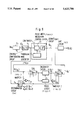
- FIG. 1 is a schematic diagram of the main circuit and the control circuit showing an embodiment of a power converter control system of this invention
- FIG. 2 is a characteristic graph to illustrate the operation of the control system in FIG. 1;
- FIG. 3 is a time chart to illustrate the operation of the system in FIG. 1;
- FIG. 4 is a block diagram of the gate circuit GC of the system in FIG. 1;
- FIG. 5 is a time chart to illustrate the operation of the gate circuit GC in FIG. 4;
- FIG. 6 is a schematic diagram of the main circuit and the control circuit showing another embodiment of a power converter control system of this invention.
- FIG. 7 is a characteristic graph to illustrate the control operation of the system in FIG. 6;
- FIG. 8 is a time chart to illustrate the control operation in FIG. 6;
- FIG. 9 is a control block diagram showing a further embodiment of the power converter control system of this invention.
- FIG. 10 is a flow-chart to illustrate the operating process of FIG. 9;
- FIG. 11 is a diagram to illustrate PWM control operation in FIG. 9 when the voltage command value is positive;
- FIG. 12 is a diagram to illustrate PWM control operation in FIG. 9 when the voltage command value is negative;
- FIG. 13 is a schematic diagram of the main circuit and the control circuit to illustrate a prior art power converter control system
- FIG. 14 is a time chart to illustrate the prior art control system in FIG. 13.
- FIG. 1 shows an embodiment of a power converter control system of this invention.
- FIG. 1(a) is a schematic diagram of the main circuit
- FIG. 1(b) is a block diagram of the control circuit.
- V d1 , V d2 are DC voltage sources
- S 1 , S 2 are self-turn-off devices
- D 1 , D 2 are free-wheeling diodes
- LOAD is load
- CT u is current detector.
- the composition of this main circuit is the same as that in FIG. 13(a).
- comparator C u current control compensation circuit G u (S)
- FX function generator
- V/f voltage/frequency converter
- TRG triangular wave generator
- PWM control circuit pulse-width modulation control circuit
- PWMCA pulse-width modulation control circuit
- U-phase load current I u is detected by current detector CT u , and is inputted to comparator C u of the current control circuit.
- This deviation ⁇ u is amplified by the following control compensation circuit G u (S) to Generate voltage command value e u .
- This voltage command value e u is inputted to PWM control circuit PWMCA and, at the same time, is inputted to function generator FX.
- Output signal e 0 of function generator FX is inputted to the following voltage/frequency converter V/f, and is converted by voltage/frequency conversion to a clock signal of frequency f CL proportional to e 0 .
- This clock signal is inputted to the following triangular wave generator TRG and determines the carrier wave frequency f c of PWM control.
- ⁇ E a , and becomes f c f c0 ⁇ (1-
- ⁇ k MAX , and becomes f c f c0 ⁇ (1-
- FIG. 3 shows an example of the PWM control operation of the system in FIG. 1.
- e u is voltage command value
- X is carrier wave (triangular wave) signal
- +k MAX and -k MAX shown by the pecked lines are the maximum modulation factors of prior art PWM control
- g u is the signal
- end V u is inverter output voltage.
- V u +V d /2, when S 1 is ON (S 2 is OFF);
- V u -V d /2, when S 2 is ON (S 1 is OFF).
- Mean value MV u of inverter output voltage V u becomes a value proportional to voltage command value e u .
- the "1" and "0" periods of gate signal g u always becomes longer than the minimum ON time (or minimum OFF time) ⁇ t of devices S 1 and S 2 which compose the inverter. Thus there is no problem of any kind.
- PWM control carrier wave frequency f c f c0 ⁇ (1-e u )/(1-k MAX ).
- mean value MV of inverter output voltage V u becomes a value proportional to voltage command value e u in the same way as in normal PWM control.
- mean value MV u of inverter output voltage V u can be obtained as a value proportional to voltage command value e u even in the region of e u >+k MAX . Also, the minimum ON time (minimum OFF time) ⁇ t of devices S 1 and S 2 which compose the inverter can be satisfied.
- mean value MV u of inverter output voltage V u becomes a value proportional to voltage command value e u .
- the period ⁇ t of gate signal g u 1 becomes constant, and the minimum ON time (minimum OFF time) of devices S 1 and S 2 which compose the inverter can be satisfied.
- gate signal g u should be processed by gate circuit GC so that the minimum ON time (or minimum OFF time) of the devices are satisfied whatever the case may be.
- FIG. 4 shows gate circuit GC of the system in FIG. 1.
- IN is an inversion circuit
- MMA1 to MMA3 and MMB1 to MMB3 are monomulti circuits
- AND1 and AND2 are AND circuits
- OR1 and OR2 are OR circuits.
- FIG. 5 shows a time chart to illustrate the operation of FIG. 4.
- g u is a gate signal
- Ig u is an inversion signal of gate signal g u obtained via inversion circuit IN;
- m 1a is an output signal of monomulti MMA1 which operates at the falling of gate signal g u ;
- m 2a is an output signal of monomulti MMA2 which operates at the falling of gate signal g u ;
- m 3a is an output signal of monomulti MMA3 which operates at the falling of output signal m 2a ;
- m 1b is an output signal of monomulti MMB1 which operates at the falling of inversion signal Ig u ;
- m 2b is an output signal of monomulti MMB2 which operates at the falling of inversion signal Ig u ;
- m 3b is an output signal of monomulti MMB3 which operates at the falling of output signal m 2b ;
- g 1 and g 2 are gate signals of devices S 1 and S 2 .
- Gate signals g 1 and g 2 are obtained by executing the following logic operations following the circuit in FIG. 4.
- Im 2a is taken as an inversion value of signal m 2a
- Im 2b is an inversion value of signal m 2b .
- Monomulti circuits MMA1 and MMA2 operate when signal g u shifts from “1" to “0". However, when signal m 1b is 0, it provides an interlock so that they do not operate. Similarly, monomulti circuits MMB1 and MMB2 operate when inversion signal Ig u shifts from "1" to "0". However, when signal m 1a is 0, it provides an interlock so that they do not operate.
- Gate signal g 1 of device S 1 is obtained by the logic operation described above, and becomes "0" only during time t OFF from the point of the falling of gate signal g u ', and this satisfies the minimum OFF time of device S 1 . Also, gate signal g 2 of device S 2 becomes "1" delayed only by time t D from the point of the falling of signal g u , and device S 2 is caused to be ON only duping time t ON . Therefore, this satisfies the minimum ON time of device S 2 .
- gate signal g 2 of device S 2 becomes "0" only during the time t OFF from the point of the falling of inversion signal Ig u , and this satisfies the minimum OFF time of device S 2 .
- gate signal g 1 of device S 1 becomes "1" delayed only by time t D from the point of the falling of inversion signal Ig u , and device S 1 is caused to be ON only during time t ON . Therefore, this satisfies the minimum ON time of device S 1 .
- output voltage V u of inverter proportional to voltage command value e u can be continuously obtained even in the region where the absolute value of voltage command value e u is greater than the maximum modulation factor k MAX of the PWM control. Also, it is possible to satisfy the minimum ON time or minimum OFF time of the devices which compose the converter. As a result, when exercising PWM control of power converters such as inverters or converters, the utilization factor of the converter can be greatly increased. Thus, reduction in the voltage V d of the DC power becomes possible. Therefore reduction in size of the converter, increased efficiency and cost-reduction can be achieved.
- FIG. 6 shows another embodiment of the power converter control system of this invention.
- FIG. 6(a) is a schematic diagram of the main circuit
- FIG. 6(b) is a block diagram of its control circuit.
- V d1 , V d2 are DC voltage sources
- S 1 , S 2 are self-turn-off devices
- D 1 , D 2 are free-wheeling diodes
- LOAD load
- CT u current detector.
- the composition of this main circuit is the same as that in FIG. 1(a). However, the composition of the control circuit in FIG. 6(b) differs. That is to say the control circuit shown in FIG.
- 6(b) is composed of comparator C u , current control compensation circuit G u (S), an adder A 1 , a subtractor A 2 , sample hold circuits SH 1 , SH 2 , a signal correction circuit SX, pulse-width modulation control circuit (PWM control circuit) PWMC and gate circuit GC.
- This drawing shows only the portion for one phase (e.g. the U phase). In the case of a 3-phase load, the portions for the other two phases (V and W phases) are composed in the same way.
- U-phase load current I u is detected by current detector CT u , and is inputted to comparator C u of the current control circuit.
- This deviation ⁇ u is amplified by the following control compensation circuit G u (S) to generate an original voltage command value e u .
- This original voltage command value e u is inputted to adder A 1 and added to an error signal ⁇ e which is held by second sample hold circuit SH 2 .
- Output signal e 1 of that sample hold circuit SH 1 is inputted to the following signal correction circuit SX, and is converted to a new voltage command value e 2 depending on its size.
- FIG. 7 shows a practical example of the input/output characteristics of signal correction circuit SX.
- the input is output signal e 1 from sample hold circuit SH 1 .
- New voltage command value e 2 is outputted by comparing signal e 1 and level setting values E a and E b (0 ⁇ E a ⁇ E b ⁇ 1) such that
- This voltage command value e 2 is inputted to PWM control circuit PWMC in FIG. 6.
- Gate circuit GC receives output gate signal g u of PWM control circuit PWMC, and outputs gate signals g 1 and g 2 for self-turn-off devices S 1 and S 2 .
- the circuit compositions of PWM control circuit PWMC and gate circuit GC are respectively the same as those in FIG. 13(b) and FIG. 4.
- level setting value E a is set equal to the maximum modulation factor K MAX OF PWM control.
- Second sample hold circuit SH 2 operates in synchronization with PWM control carrier wave signal X from PWM control circuit PWMC, however it operates by shifting its timing slightly from the operation of first sample hold circuit SH 1 .
- e u shows original voltage command value
- X is PWM control carrier wave signal
- e 2 is new PWM control input signal
- SP 1 and SP 2 are timing signals for sample hold circuits SH 1 and SH 2 when e u >0
- SP 1 ' and SP 2 ' are timing signals for sample hold circuits SH 1 and SH 2 when e u >0
- g u is gate signal
- V u is inverter output voltage
- sample hold circuits SH 1 and SH 2 operate with timing signals SP 1 and SP 2 .
- first sample hold circuit SH 1 is operated in synchronization with PWM control carrier wave signal (carrier signal) X, and takes in the sum of original voltage command value e u and error signal ⁇ e held in second sample hold circuit SH 2 .
- sample hold circuit SH 1 When original voltage command value e u has become e u ⁇ -E a , sample hold circuit SH 1 operates by timing signal SP 1 ' at times t 0 ', t 1 ', t 2 '. Sample hold circuit SH 2 operates by timing signal SP 2 ' at times delayed by time t d , respectively.
- Carrier wave frequency f c of PWM control circuit PWMC in the embodiment in FIG. 6 differs from that in the embodiment in FIG. 1, and is constant.
- FIG. 9 shows part, that is to say the U-phase only, of the power converter control system of the PWM control of this invention.
- SW1 and SW2 are switches which operate in response to the output signals of discrimination circuit Ga;
- CAL is a calculation circuit which has a memory which stores an error time ⁇ ti when a pulse width ti of a control pulse Pi is narrower than a set time ts, as described later;
- TCONT is a pulse circuit which outputs pulse Ps of a width of set time ts.
- INV1 and INV2 are inversion circuits.
- control pulse Pi(g u ) which is obtained by the comparison of voltage command value e u and triangular wave X from carrier wave generator TRG, is inputted to a terminal b of switch SW1 and to inversion circuit INV1. Voltage command value e u is inputted to discrimination circuit Ga. Also, an output signal IPi of inversion circuit INV1 is inputted to a terminal c of switch SW1, and output signal Sk of discrimination circuit Ga is inputted to switches SW1 and SW2.
- Pulse circuit TCONT outputs pulse Ps in synchronization with input pulse Pi to calculation circuit CAL.
- Calculation circuit CAL executes a logic operation using inputted pulses Pi and Ps, and outputs pulse Po. This is inputted to a terminal e of switch SW2 and to inversion circuit INV2.
- Output pulse IPo of inversion circuit INV2 is inputted to a terminal f of switch SW2.
- Gate circuit GC receives gate signal g u ' and outputs gate signal g 1 and g 2 for self-turn-off devices S 1 and S 2 .
- FIG. 10 shows an operation flow-chart for calculation circuit CAL. This describes the case of voltage command value e u is e u >0.
- ti is the pulse-width of input pulse Pi selected by switch SW1
- ts shows the width of pulse Ps for time-setting.
- Calculation circuit CAL measures the pulse-width ti and ts of the initially inputted pulses Pi and Ps using commonly-known methods.
- ti n is the pulse-width of control pulse Pi obtained by the comparison of voltage command value e u and triangular wave X, and ts shows the set time (-t off ; minimum OFF time of the device), where n is the number of the input pulse.
- Pulse-width ti 5 of fifth control pulse Pi is wider than set time ts.
- output pulse Po is inputted as it stands from terminal d to gate circuit GC as gate signal g u '.
- Input pulse Pi is inverted by inversion circuit INV1 and is inputted to calculation circuit CAL as inverted pulse IPi, and calculation is executed in the same way as in FIG. 10.
- pulse-width ti should be read as the pulse-width of inverted pulse IPi in FIG. 10.
- the output pulse Po of calculation circuit CAL is inverted by inversion circuit INV2 and becomes inverted pulse IPo. This is inputted to gate circuit GC from terminal d as gate signal g u '.
- pulse-width ti' of adjusted control pulse Pi and the set time ts are compared.
- a control pulse Po of pulse-width ti' is outputted as it stands.
- output voltage of the power converter can continuously be obtained proportional to voltage command value, by adding error time to pulse-width of control pulse; finding new control pulse-width; comparing this new pulse-width with set time and outputting a control pulse in response to that result, even if the absolute value of the voltage command value is in the region where it is greater than the maximum modulation factor of PWM control. Also, it is possible to satisfy the minimum ON time or minimum OFF time of the devices which compose the converter.
Abstract
A control system for a pulse-width modulation controlled power converter composed of self-turn-off devices. The control system includes a voltage command value generator for the power converter, a carrier wave generator and a circuit for correcting at least one of the voltage command value and the frequency of the carrier wave to generate as a corrected voltage command value and a corrected carrier wave. The control system further includes a gate pulse signal generator for receiving a first signal and a second signal and for comparing the first and second signals to generate gate pulse signals to the self-turn-off devices for controlling the power converter based on a comparison result. The voltage command value is taken as e (-1≦e≦+1), and a level setting value is taken as Ea (0<Ea <1). The gate pulse signal generator receives the voltage command value and the carrier wave as the first and second signals when -Ea ≦e≦+Ea. The gate pulse signal generator receives one of the voltage command value and the corrected voltage command value as the first signal and one of the carrier wave and she corrected carrier wave as the second signal when e<-Ea or +Ea <e.
Description
This application is a Continuation of application Ser. No. 08/187,490, filed on Jan. 28, 1994, now abandoned
1. Field of the Invention
This invention relates to a power converter control system, and more particularly to a control system for pulse-width modulation-controlled (PWM control) converters which convert AC power to DC power and PWM control inverters which convert DC power to AC power.
2. Description of the Related Art
FIG. 13 shows a schematic diagram of one phase (the U phase) of a prior art PWM control inverter. FIG. 13(a) shows the main circuit of a power converter.
In FIG. 13(a), Vd1, Vd2 are DC voltage sources, S1, S2 are self-turn-off devices, D1, D2 are free-wheeling diodes, LOAD is a load and CTu is a current detector. Also, FIG. 13(b) shows the control circuit for the power converter. Here, Cu, C1 are comparators, Gu (S) is a current control compensation circuit, PWMC is a pulse-width modulation control circuit, TRG is a carrier wave generator, SM is a Schmitt circuit and GC is a gate circuit. Here, load current Iu is detected by current detector CTu. This is compared with a current command value IuO by comparator Cu and a deviation εu =IuO -Iu is found. This deviation εu is amplified by current control compensation circuit Gu (S) to generate a voltage command value eu =Gu (S)·εu, which is inputted to pulse-width modulation control circuit PWMC.
In pulse-width modulation control circuit PWMC, carrier wave generator TRG generates a triangular wave X. This is compared with inputted signal eu by comparator C1, and a gate signal gu is produced via Schmitt circuit SM. Gate circuit GC inputs this gate signal gu and produces gate signals g1 and g2 and for self-turn-off devices S1 and S2. The composition of this circuit explained later.
The example described above is an example for single phase output inverters, e.g. U phase, only. In the case of 3-phase output inverters, apart from this, the V and W phase circuits also have similar compositions.
In the following explanation, voltage command value eu and its related values KMAX, X, Ea and Eb use normalized values.
FIG. 14 is a time chart to illustrate the operation of PWM control circuit PWMC in FIG. 13. That is to say,
When eu ≧X, gu =1 and S1 : ON (S2 :OFF).
When eu <X, gu =0 and S1 :OFF (S2 :ON)
At this time, when DC power source voltages Vd1, Vd2 are taken as Vd1 =Vd2 =Vd /2, inverter output voltage Vu becomes
Vu =+Vd /2, when S1 is ON (S2 is OFF): and
Vu =-Vd /2, when S1 is OFF (S2 is ON).
The mean value MVu of inverter output voltage Vu (shown by the pecked line) becomes a value proportional to input signal eu. Therefore, this input signal eu becomes the inverter voltage command value.
When IuO >Iu, deviation εu =IuO-I u becomes a positive value, and voltage command value eu increases. Therefore, inverter output voltage Vu increases in proportion to eu and increases load current Iu.
Conversely, when IuO <Iu, deviation εu =IuO -Iu becomes a negative value and voltage command value eu decreases. Therefore, inverter output voltage Vu decreases and this decreases load current Iu.
Control is exercised so that, finally, Iu =IuO. When current command value IuO is changed as sine wave form, load current Iu also is controlled to follow this, and a sine wave current can be supplied to load LOAD.
In this way PWM control inverters can obtain output voltage Vu proportional to voltage command value eu. They are therefore widely used in the driving systems of AC motors as variable voltage variable frequency power sources.
However, prior art PWM control inverters have the following problem.
Self-turn-off devices such as gate turn-off thyristors (GTO) are used as devices which compose the inverter. However, in order to protect these self-turn-off devices (hereafter, "devices"), well-known, snubbey circuits are connected in parallel to the devices. When the device is temporarily switched ON in order to initialize (discharge) the capacitor of this snubber circuit, a constant-time ON state must be maintained for the device. Also, minimum ON, OFF times are determined by the characteristic of the device itself, and the pulse-width of the gate signal is supplied to satisfy this.
In FIG. 14, +kMAX and -kMAX express an upper limit value and a lower limit value of voltage command value eu. Output voltage Vu, which is proportional to this voltage command value eu within the limits +kMAX ≧eu ≧-kMAX can be generated.
When eu =+kMAX, the period of gate signal gu =0 becomes Δt, and this satisfies the minimum ON time of device S2 (the minimum OFF time of device S1). Similarly, when eu =-kMAX, the period of gate signal g u 1 becomes Δt, and this satisfies the minimum ON time of device S1 (the minimum OFF time of device S2).
When eu >+kMAX or eu <-kMAX, the period of gate signal gu =0 or gu =1 becomes shorter than Δt. Therefore, the minimum ON or OFF times of the devices cannot be satisfied. Because of this, the voltage command value eu is controlled to be within the limits of +kMAX ≧eu ≧-kMAX by providing a limiter circuit or the like (not illustrated).
For example, when the carrier frequency fc is taken as fc =500 Hz, cycle T of triangular wave X becomes 2 msec, and in order to satisfy the minimum ON time (or minimum OFF time) Δt=200 μsec, kMAX =0.8. That is to say, in this case the utilization factor of the inverter is 80%, and the remaining 20% is redundant.
Therefore, a greater inverter capacity had to be prepared for the portion by which the utilization factor was reduced. Thus, the prior art PWM control inverter was an uneconomic system.
Accordingly, one object of this invention is to provide a power converter control system which executes control so that an output voltage proportional to the input signal can be generated, while ensuring the minimum ON time or the minimum OFF time of the device, and thus can increase the utilization factor of the converter, even when the absolute value of that input signal(the voltage command value) is great,
Another object of this invention is to provide a power converter control system which can reduce the voltage of the DC power source and in which reduction in size of the power converter, increased efficiency and cost reduction can be achieved.
These and other objects of this invention can be achieved by providing a control system for a pulse-width modulation controlled power converter composed of self-turn-off devices. The control system includes a voltage command value generator for the power converter, a carrier wave generator and a circuit for correcting at least one of the voltage command value and the frequency of the carrier wave to generate as a corrected voltage command value and a corrected carrier wave. The control system further includes a gate pulse signal generator for receiving a first signal and a second signal and for comparing the first and second signals to generate gate pulse signals to the self-turn-off devices fop controlling the power converter based on a comparison result. The voltage command value is taken as e (-1≦e≦+1), and a level setting value is taken as Ea (0<Ea <1). The gate pulse signal generator receives the voltage command value and the carrier wave as the first and second signals when -Ea ≦e≦+Ea. The gate pulse signal generator receives one of the voltage command value and the corrected voltage command value as the first signal and one of the carrier wave and the corrected carrier wave as the second signal when e<-Ea or +Ea <e.
According to one aspect of this invention, there is provided a control system for a pulse-width modulation controlled power converter composed of self-turn-off devices. The control system includes a voltage command value generator for the power converter, a carrier wave generator and a circuit for correcting the frequency of the carrier wave to generate as a corrected carrier wave. The control system further includes a gate pulse signal generator for receiving a first signal and s second signal and for comparing the first and second signals to generate gate pulse signals to the self-turn-off devices for controlling the power converter based on a comparison result. The voltage command value is taken ss e (-1≦e≦+1), and a level setting value is taken as Ea (0<Ea <1). The gate pulse signal generator receives the voltage command value and the carrier wave as the first and second signals when -Ea ≦e≦+Ea. The gate pulse signal generator receives the voltage command value as the first signal and the corrected carrier wave as the second signal when e<-Ea or +Ea <e.
According to another aspect of this invention, there is provided a control system for a pulse-width modulation controlled power converter composed of self-turn-off devices. The control system includes a voltage command value generator for the power converter, a carrier wave generator and a circuit for correcting the voltage command value to generate as a corrected voltage command value. The control system further includes a gate pulse signal generator for receiving a first signal and a second signal and for comparing the first and second signals to generate gate pulse signals to the self-turn-off devices for controlling the power converter based on a comparison result. The voltage command value is taken as e (-1≦e≦+1), and a level setting value is taken as Ea (0<E<1). The gate pulse signal generator receives the voltage command value and the carrier wave as the first and second signals when -Ea ≦e≦+Ea. The gate pulse signal generator receives the corrected voltage command value as the first signal and the carrier wave as the second signal when e<-Ea or +Ea <e.
These and other objects of this invention can be further achieved by providing a control system for a pulse-width modulation controlled power converter composed of self-turn-off devices. The control system includes a voltage command value generator for the power converter, a carrier wave generator and a gate pulse signal generator for receiving the voltage command value and the carrier wave and for comparing the voltage command value and the carrier wave to generate gate pulse signals based on a comparison result. The control system further includes a correction circuit connected to receive the voltage command value and the gate pulse signals for generating corrected gate pulse signals to the self-turn-off devices for controlling the power converter. The voltage command value is taken as e (-1≦e≦+1), and a level setting value is taken as Ea (0<Ea <1). The correction circuit generates the gate pulse signals as the corrected gate pulse signals as they stand, when -Ea ≦e≦+Ea. The correction circuit corrects a pulse-width (ti) of the gate pulse signals when e<-Ea or +Ea <e, and generates gate pulse signals with a corrected pulse-width (ti') as the corrected gate pulse signals only when the corrected pulse-width (ti') is equal to or larger than a set time (ts).
The following operation can be obtained when using this invention. Normally, voltage command value e (-1≦e≦+1) is supplied from the circuit which controls the output current of the power converter.
When the maximum modulation factor of PWM control is taken as kMAX (0<kMAX <1), the output voltage of the power converter is controlled by normal pulse-width modulation control when -kMAX ≦e≦+kMAX.
Also, when e<-kMAX or +kMAX <e, the output voltage of the power converter is controlled by adjusting the pulse interval of the pulse with the constant width Δt which satisfies the minimum ON time (or minimum OFF time) of the device.
The following further operation can be obtained when using this invention. That is to say, when the carrier wave frequency of normal PWM control is taken as Fco, the carrier wave frequency of the PWM control circuit is altered such that fc =fco ·(1-|e|)/(1-kMAX) when e<-kMAX or kMAX <e. If a gate signal is produced by comparing this new carrier wave (triangular wave) and voltage command value e, a pulse with an almost constant width Δt can be obtained, Moreover, since frequency fc reduces as the absolute value |e| of voltage command value e approaches, 1, a voltage proportional to voltage command value e can be obtained for the output voltage of the power converter even when voltage command value e is within the region of e<-kMAX or +kMAX <e.
In this way, when using the power converter control system of this invention, e voltage proportional to voltage command value e is obtained for the output voltage of the power converter even when voltage command value e is within the region of e<-kMAX or +kMAX <e. Moreover, a pulse with a constant width At which satisfies the minimum ON time (or minimum OFF time) of the device can be obtained. Therefore it is possible to increase the utilization factor of the power converter to 100%, end the prior art problem can be solved.
That is to say, it is possible to continue to obtain output voltage Vu proportional to voltage command value eu even in the region where the absolute value of the voltage command value eu is greater than the maximum modulation factor kMAX of the PWM control. In addition, it is possible to satisfy the minimum ON time or the minimum OFF time of the devices which compose the converter. As a result, in the case of PWM control of a power converter such as an inverter or a converter, it is possible greatly to increase the utilization factor of that converter. Also, it is possible to reduce the voltage Vd of the DC power source by that amount. Thus, it becomes possible to achieve reduction in size, increased efficiency and cost-reduction of the converter.
When using this invention, the following still further operation can be obtained. That is to say, it is possible to generate voltage Vu from the converter proportional to voltage command value eu mean value-wise, while selecting either the generation of a pulse which satisfies the minimum ON time (or minimum OFF time) Δt of the device or the elimination of generating that pulse, when the original voltage command value eu is within the regions eu <-Ea or eu >+Ea. As a result, it becomes possible to increase the utilization factor of the converter up to 100%.
When using this invention, the following yet further operation can be obtained. That is to say, when voltage command value e is -kMAX ≦e≦+kMAX, the output voltage of the power converter is controlled by normal pulse-width modulation control. Also, when e<-kMAX or +kMAX <e, a pulse-width Δti'=ti+Δti of a new control pulse is obtained by adding an error time Δti to a width ti of a control pulse Pi. This pulse-width ti' is compared with a set time ts. When ti'≧ts, the output pulse is outputted and, at the same time, Δti=0 is stored in the memory. When ti'<ts, Δt=ti' is stored in the memory without outputting the output pulse. Then, error time Δti is controlled so that it is reflected in the following control pulse. As a result, it is possible to obtain an output voltage which is proportional to the voltage command value e. Moreover, it is possible to satisfy the minimum OFF time (or minimum ON time) of the device. Therefore, it becomes possible to increase the utilization factor of the converter to 100% and thus to solve the prior art problem.
A more complete appreciation of the invention and many of the attendant advantages thereof will be readily obtained as the same becomes better understood by reference to the following detailed description when considered in connection with the accompanying drawings, wherein:
FIG. 1 is a schematic diagram of the main circuit and the control circuit showing an embodiment of a power converter control system of this invention;
FIG. 2 is a characteristic graph to illustrate the operation of the control system in FIG. 1;
FIG. 3 is a time chart to illustrate the operation of the system in FIG. 1;
FIG. 4 is a block diagram of the gate circuit GC of the system in FIG. 1;
FIG. 5 is a time chart to illustrate the operation of the gate circuit GC in FIG. 4;
FIG. 6 is a schematic diagram of the main circuit and the control circuit showing another embodiment of a power converter control system of this invention;
FIG. 7 is a characteristic graph to illustrate the control operation of the system in FIG. 6;
FIG. 8 is a time chart to illustrate the control operation in FIG. 6;
FIG. 9 is a control block diagram showing a further embodiment of the power converter control system of this invention;
FIG. 10 is a flow-chart to illustrate the operating process of FIG. 9;
FIG. 11 is a diagram to illustrate PWM control operation in FIG. 9 when the voltage command value is positive;
FIG. 12 is a diagram to illustrate PWM control operation in FIG. 9 when the voltage command value is negative;
FIG. 13 is a schematic diagram of the main circuit and the control circuit to illustrate a prior art power converter control system; and
FIG. 14 is a time chart to illustrate the prior art control system in FIG. 13.
Referring now to the drawings, wherein like reference numerals designate identical or corresponding parts throughout the several views, the embodiments of this invention will be described below.
FIG. 1 shows an embodiment of a power converter control system of this invention. FIG. 1(a) is a schematic diagram of the main circuit, and FIG. 1(b) is a block diagram of the control circuit.
In FIG. 1(a), Vd1, Vd2 are DC voltage sources, S1, S2 are self-turn-off devices D1, D2 are free-wheeling diodes, LOAD is load and CTu is current detector. The composition of this main circuit is the same as that in FIG. 13(a). As shown in FIG. 1(b), comparator Cu, current control compensation circuit Gu (S), a function generator FX, a voltage/frequency converter V/f, triangular wave generator TRG and a pulse-width modulation control circuit (PWM control circuit) PWMCA are provided as the control circuit. PWM control circuit PWMCA is composed of comparator C1, Schmitt circuit SM and gate circuit GC.
This drawing only shows the portion for one phase (e.g. the U phase). In the case of a 3-phase load, the portions for the other two phases (V and W phases) are composed in the same way.
U-phase load current Iu is detected by current detector CTu, and is inputted to comparator Cu of the current control circuit. Comparator Cu compares current command value IuO and current detection value Iu, and finds the deviation εu =IuO -Iu. This deviation εu is amplified by the following control compensation circuit Gu (S) to Generate voltage command value eu.
This voltage command value eu is inputted to PWM control circuit PWMCA and, at the same time, is inputted to function generator FX.
FIG. 2 shows a practical example of the input/output characteristics of function generator FX. That is to say, when the absolute value of input signal eu is at or below a certain level setting value Ea (0≦Ea ≦1), the output signal is taken as e0 =E0 =constant. When the absolute value of input signal eu is greater than Ea, the output signal is taken as e0 =E0 ·(1-|eu |)/(1-Ea).
Output signal e0 of function generator FX is inputted to the following voltage/frequency converter V/f, and is converted by voltage/frequency conversion to a clock signal of frequency fCL proportional to e0. This clock signal is inputted to the following triangular wave generator TRG and determines the carrier wave frequency fc of PWM control.
That is to say, frequency fc of triangular wave X becomes constant at fc =fco when the absolute value of voltage command value eu is |eu |≦Ea, and becomes fc =fc0 ·(1-|eu |)/(1-Ea) when |eu |>Ea.
When the maximum modulation factor of PWM control is taken as kMAX and it is set that Ea =kMAX, frequency fc of triangular wave X becomes constant (fc =fc0) when |eu |≦kMAX, and becomes fc =fc0 ·(1-|eu |)/(1-kMAX) when |eu |>kMAX.
FIG. 3 shows an example of the PWM control operation of the system in FIG. 1. In the drawing, eu is voltage command value, X is carrier wave (triangular wave) signal, +kMAX and -kMAX shown by the pecked lines are the maximum modulation factors of prior art PWM control, gu is the signal, end Vu is inverter output voltage.
The following is a description of the case when Ea =kMAX is set. When -kMAX ≦eu ≦+kMAX, the frequency of PWM control carrier wave becomes constant (fc =fc0), and normal pulse-width modulation control is executed. In PWM control, voltage command value eu end triangular wave X are compared, and gate signal gu of devices S1 and S2 produced. That is to say,
when eu ≧X, gu =1 and S1 :ON (S2 :OFF); and
when eu ≧X, gu =0 and S2 :ON (S1 :OFF).
When the DC source voltage Vd1, Vd2 are taken as Vd1 =Vd2 =Vd /2, the output voltage Vu of the inverter becomes
Vu =+Vd /2, when S1 is ON (S2 is OFF); and
Vu =-Vd /2, when S2 is ON (S1 is OFF).
Mean value MVu of inverter output voltage Vu becomes a value proportional to voltage command value eu. In this case the "1" and "0" periods of gate signal gu always becomes longer than the minimum ON time (or minimum OFF time) Δt of devices S1 and S2 which compose the inverter. Thus there is no problem of any kind.
Next, the operation when eu >+kMAX ts described with reference to FIG. 3 In the region of eu >+kMAX, PWM control carrier wave frequency fc is obtained by fc =fc0 ·(1-eu)/(1-kMAX). When gate signal gu is produced by comparing this carrier wave (triangular wave) X and voltage command value eu,
when eu ≧X, gu =1 and S1 :ON (S2 :OFF); and
when eu <X, gu =0 and S2 :ON (S1 :OFF).
Thus, mean value MV of inverter output voltage Vu becomes a value proportional to voltage command value eu in the same way as in normal PWM control. When taking the cycle of triangular wave X as Tc =1/fc and the period of gate signal gu =0 as Δt, mean value MVu of inverter output voltage Vu is
MV.sub.u =(V.sub.d /2)·(T.sub.c -2·Δt)/T.sub.c.
Since this is proportional to voltage command value eu, the relationship
e.sub.u =(T.sub.c -2·Δt)/T.sub.c
is established, and therefore ##EQU1##
Thus period Δt becomes a constant value regardless of command value eu even in the region of eu.
In this way, mean value MVu of inverter output voltage Vu can be obtained as a value proportional to voltage command value eu even in the region of eu >+kMAX. Also, the minimum ON time (minimum OFF time) Δt of devices S1 and S2 which compose the inverter can be satisfied.
In the same way also, when eu <-kMAX, mean value MVu of inverter output voltage Vu becomes a value proportional to voltage command value eu. Also, the period Δt of gate signal gu =1 becomes constant, and the minimum ON time (minimum OFF time) of devices S1 and S2 which compose the inverter can be satisfied.
In the actual system, when carrier wave frequency fc is changed following voltage command value eu, an operation error is generated, and also there is sometimes a problem with the accuracy of triangular wave X. As a result, when eu <+kMAX, the period when the gate signal gu should become gu =0 (or when eu >-kMAX, the period when the gate signal gu should become gu =1) does not become accurately equal to Δt. In this case, it is allowable for inverter output voltage Vu to be controlled with a certain degree of error in relation to voltage command value eu. However, if the minimum ON time (or minimum OFF time) Δt of devices S1 and S2 cannot be satisfied, there will be a risk of the devices S1 and S2 being damaged. Therefore, gate signal gu should be processed by gate circuit GC so that the minimum ON time (or minimum OFF time) of the devices are satisfied whatever the case may be.
FIG. 4 shows gate circuit GC of the system in FIG. 1. In the drawing, IN is an inversion circuit, MMA1 to MMA3 and MMB1 to MMB3 are monomulti circuits, AND1 and AND2 are AND circuits and OR1 and OR2 are OR circuits.
Also, FIG. 5 shows a time chart to illustrate the operation of FIG. 4.
In FIG. 5,
gu is a gate signal;
Igu is an inversion signal of gate signal gu obtained via inversion circuit IN;
m1a is an output signal of monomulti MMA1 which operates at the falling of gate signal gu ;
m2a is an output signal of monomulti MMA2 which operates at the falling of gate signal gu ;
m3a is an output signal of monomulti MMA3 which operates at the falling of output signal m2a ;
m1b is an output signal of monomulti MMB1 which operates at the falling of inversion signal Igu ;
m2b is an output signal of monomulti MMB2 which operates at the falling of inversion signal Igu ;
m3b is an output signal of monomulti MMB3 which operates at the falling of output signal m2b ; and
g1 and g2 are gate signals of devices S1 and S2.
Monomulti circuits MMA2 and MMB3 supply dead times tD for preventing inverter devices S1 and S2 switching ON simultaneously. Also, monomulti circuits MMA1 and MMB1 supply minimum OFF times tOFF for the devices, and monomulti circuits MMA3 and MMB3 supply minimum ON times tON for the devices. These have the relationship tON =tOFF -2·tD.
Gate signals g1 and g2 are obtained by executing the following logic operations following the circuit in FIG. 4. Here, Im2a is taken as an inversion value of signal m2a and Im2b as an inversion value of signal m2b.
g.sub.1 =g.sub.u ×m.sub.1a ×Im.sub.2b +m.sub.3b
g.sub.2 =Ig.sub.u ×m.sub.1b ×Im.sub.2a +m.sub.3a.
When gate signal g1 is "1", device S1 is ON, and when it is "0", S1 is OFF. Also, when gate signal g2 is "1", device S2 is ON, and when it is "0", device S2 is OFF. There is a dead time tD when devices S1 and S2 are shifting between ON and OFF respectively, and this prevents devices S1 and S2 being ON simultaneously.
Monomulti circuits MMA1 and MMA2 operate when signal gu shifts from "1" to "0". However, when signal m1b is 0, it provides an interlock so that they do not operate. Similarly, monomulti circuits MMB1 and MMB2 operate when inversion signal Igu shifts from "1" to "0". However, when signal m1a is 0, it provides an interlock so that they do not operate.
First, the case when period Δt1 of gu =0 has become shorter than minimum OFF time tOFF is described. Monomulti circuits MMA1 and MMA2 operate through the falling of signal gu. Signal m1a becomes "0" only during time tOFF, and signal m2a becomes "1" only during time tD. Also, monomulti circuit MMA3 operates at the falling of signal m2a. Signal m3a becomes "1" only during time tON. Inversion signal Igu falls at time Δt1 after the fall of signal gu. However, since signal m1a has already become "0", MMB1, MMB2 and MMB3 will not operate. Gate signal g1 of device S1 is obtained by the logic operation described above, and becomes "0" only during time tOFF from the point of the falling of gate signal gu ', and this satisfies the minimum OFF time of device S1. Also, gate signal g2 of device S2 becomes "1" delayed only by time tD from the point of the falling of signal gu, and device S2 is caused to be ON only duping time tON. Therefore, this satisfies the minimum ON time of device S2.
Next, the case when period Δt2 of signal gu =1 has become shorter than minimum OFF time tOFF is described. Monomulti circuits MMB1 and MMB2 operate through the falling of inversion signal Igu. Signal m1b becomes "0" only during time tOFF, and signal m2b becomes "1" only during time tD. Also, monomulti circuit MMB3 operate at the falling of signal m2b. Thus signal m3b becomes "1" only during time tON. Signal gu falls at time Δt2 after the fall of inversion signal Igu. However, since signal m1b has already become "0", MMA1, MMA2 and MMA3 will not operate. As a result, gate signal g2 of device S2 becomes "0" only during the time tOFF from the point of the falling of inversion signal Igu, and this satisfies the minimum OFF time of device S2. Also, gate signal g1 of device S1 becomes "1" delayed only by time tD from the point of the falling of inversion signal Igu, and device S1 is caused to be ON only during time tON. Therefore, this satisfies the minimum ON time of device S1.
In this gate circuit, when the period in which gate signal gu becomes "1" or "0" becomes longer than minimum OFF time tOFF, gate signals g1 and g2 are outputted as they stand by taking only dead time tD into consideration. That it to say, at point p in FIG. 5, signal gu falls and monomulti circuits MMA1 to MMA3 operate. However, since the period in which gu =0 after point P is longer than time tOFF, gate signal g1 becomes the same as gate signal gu. Also, gate signal g2 is delayed by dead time tD by signal m2a of monomulti circuit MMA2 and becomes g2 =1.
In this way, even if the pulse-width of gate signal becomes narrower than the minimum ON time or minimum OFF time of the device due to operational error in PWM control, this is adjusted by gate circuit GC so that the device will not be damaged. In this case, a slight error may be included in the proportional relationship between voltage command value eu and the mean value of inverter output voltage Vu, but this will not create any problem in practical use.
When using the power converter control system in the above embodiment, output voltage Vu of inverter proportional to voltage command value eu can be continuously obtained even in the region where the absolute value of voltage command value eu is greater than the maximum modulation factor kMAX of the PWM control. Also, it is possible to satisfy the minimum ON time or minimum OFF time of the devices which compose the converter. As a result, when exercising PWM control of power converters such as inverters or converters, the utilization factor of the converter can be greatly increased. Thus, reduction in the voltage Vd of the DC power becomes possible. Therefore reduction in size of the converter, increased efficiency and cost-reduction can be achieved.
FIG. 6 shows another embodiment of the power converter control system of this invention. FIG. 6(a) is a schematic diagram of the main circuit, and FIG. 6(b) is a block diagram of its control circuit.
In FIG. 6(a), Vd1, Vd2 are DC voltage sources, S1, S2 are self-turn-off devices, D1, D2 are free-wheeling diodes, LOAD is load and CTu is current detector. The composition of this main circuit is the same as that in FIG. 1(a). However, the composition of the control circuit in FIG. 6(b) differs. That is to say the control circuit shown in FIG. 6(b) is composed of comparator Cu, current control compensation circuit Gu (S), an adder A1, a subtractor A2, sample hold circuits SH1, SH2, a signal correction circuit SX, pulse-width modulation control circuit (PWM control circuit) PWMC and gate circuit GC. This drawing shows only the portion for one phase (e.g. the U phase). In the case of a 3-phase load, the portions for the other two phases (V and W phases) are composed in the same way.
U-phase load current Iu is detected by current detector CTu, and is inputted to comparator Cu of the current control circuit. Comparator Cu compares current command value IuO and current detection value Iu, and finds the deviation εu =IuO -Iu. This deviation εu is amplified by the following control compensation circuit Gu (S) to generate an original voltage command value eu. This original voltage command value eu is inputted to adder A1 and added to an error signal Δe which is held by second sample hold circuit SH2.
First sample hold circuit SH1 takes in an output signal e1 =eu +Δe of adder A1 in synchronization with the PWM control carrier wave signal X from PWM control circuit PWMC, and holds that value. Output signal e1 of that sample hold circuit SH1 is inputted to the following signal correction circuit SX, and is converted to a new voltage command value e2 depending on its size.
FIG. 7 shows a practical example of the input/output characteristics of signal correction circuit SX. The input is output signal e1 from sample hold circuit SH1. New voltage command value e2 is outputted by comparing signal e1 and level setting values Ea and Eb (0≦Ea ≦Eb ≦1) such that
______________________________________
when -E.sub.b ≧ e.sub.1'
                       e.sub.2 = -1
when -E.sub.b < e.sub.1 < -E.sub.a'
                       e.sub.2 = -E.sub.a
when -E.sub.a ≦ e.sub.1 ≦ +E.sub.a'
                       e.sub.2 = e1
when +E.sub.a < e.sub.1 < +E.sub.b'
                       e.sub.2 = +E.sub.a
when +E.sub.b ≦ e.sub.1'
                       e.sub.2 = +1.
______________________________________
This voltage command value e2 is inputted to PWM control circuit PWMC in FIG. 6. Gate circuit GC receives output gate signal gu of PWM control circuit PWMC, and outputs gate signals g1 and g2 for self-turn-off devices S1 and S2. The circuit compositions of PWM control circuit PWMC and gate circuit GC are respectively the same as those in FIG. 13(b) and FIG. 4.
The level setting values Ea end Eb of signal correction circuit SX are determined taking account of the minimum ON times Δt of the devices. For instance, when taking the maximum value Emax of the carrier wave signal as Emax =1 and the carrier frequency as fc,
1-E.sub.a =Δt·f.sub.d ·E.sub.max
1-E.sub.b =(1-E.sub.a)/2
are selected.
That is to say, level setting values Ea and Eb are selected so that when the input signal (new voltage command value e2 of PWM control circuit PWMC is e2 =Ea, the period of gate signal gu =0 which is supplied to the device becomes Δt. When taking Δt=200 μsec, fc =500 Hz, level setting values Ea and Eb become Ea =0.8 and Eb =0.9. Also, in this case, level setting value Ea is set equal to the maximum modulation factor KMAX OF PWM control.
Returning to FIG. 6, subtractor A2 computes the difference between the input and output signals of signal correction circuit SX. This is taken as error signal Δe=e1 -e2 and is inputted to second sample hold circuit SH2. Second sample hold circuit SH2 operates in synchronization with PWM control carrier wave signal X from PWM control circuit PWMC, however it operates by shifting its timing slightly from the operation of first sample hold circuit SH1.
In the case of the absolute value of original voltage command value eu being small, that is to say when -Ea ≦e1 ≦Ea new voltage command value e2 becomes e2 =e1, and the power converter is PWM controlled in the same way as in prior art. Also, the error signal Δe becomes zero and the output of second hold circuit SH2 also becomes zero.
The case of the absolute value of the PWM control input signal (voltage command value) eu having become great, that is to say the operation when eu <-Ea or eu >+Ea, is as follows. This operation is described with reference to FIG. 8, taking as an example the case when Ea =0.8, Eb =0.9 and voltage command value eu =+0.85=constant.
In FIG. 8, eu shows original voltage command value, X is PWM control carrier wave signal, e2 is new PWM control input signal, SP1 and SP2 are timing signals for sample hold circuits SH1 and SH2 when eu >0, SP1 ' and SP2 ' are timing signals for sample hold circuits SH1 and SH2 when eu >0, gu is gate signal and Vu is inverter output voltage.
Since eu >0, sample hold circuits SH1 and SH2 operate with timing signals SP1 and SP2.
First, first sample hold circuit SH1 is operated in synchronization with PWM control carrier wave signal (carrier signal) X, and takes in the sum of original voltage command value eu and error signal Δe held in second sample hold circuit SH2. First of all, when taking Δe=0 at time to, the addition value e1 becomes e1 =eu +Δe=+0.85. Therefore since +Ea <e1 <Eb, the output e2 of signal correction circuit SX becomes e2 =+E and is inputted to PWM control circuit PWMC.
In PWM control circuit PWMC the signal e2 =+Ea and carrier wave signal X are compared, and a gate signal with a pulse-width in which the period of gate signal gu =0 satisfies the minimum ON time Δt is transmitted to the power converter. The power converter Generates voltage Vu which is proportional to value +Ea =+0.8. This means that voltage Vu is outputted which is smaller by a portion proportional to e1 -Ea =0.05. Sample hold circuit SH2 is also operated in synchronization with carrier wave signal X, but it is operated delayed by a time td from sample hold circuit SH1. Therefore, Δe=e1 -Ea =0.05 is held as the error signal. This error signal Δe is once again added to voltage command value eu =+0.85. Thus, signal e1 =eu +Δe=0.9 is inputted to signal correction circuit SX by the next operation of first sample hold circuit SH1 at time t1.
Therefore this time signal e1 becomes +Ea ≦e1 ≦1, and e2 =1 is inputted to PWM control circuit PWMC. At e2 =1, there will be no period of gate signal gu =0 and the output voltage Vu of the power converter will be maximum. Therefore this means that more voltage is outputted as voltage Vu by a portion proportional to 1-eu =0.15 than in the case when original voltage command value eu is used as it stands. Since a smaller voltage was outputted under the previous control by a portion proportional to eu -Ea =0.05, in total voltage Vu will become greater by a portion proportional to 0.15-0.05=0.1. At this time, error signal Δe becomes Δe=e1 -e2 =-0.1 and is held in sample hold circuit SH2.
Furthermore, when signal eu =+0.85 is inputted at time t2, the above error signal Δe=-0.1 is added, and signal e1 =eu +Δe=0.75 is inputted to signal correction circuit SX. Therefore signal e1 becomes e1 <+Ea and voltage command value e2 =e1 =0.75 is supplied to the PWM control circuit PWMC. Therefore this means that voltage Vu is outputted which is smaller by a portion proportional to eu -e2 =0.1 than in the case when original voltage command value eu =0.85 is used at it stands. Since a greater voltage was outputted as voltage Vu under the previous control by a portion proportional to 0.1, in total the error will be zero. At this time, the error signal Δe becomes Δe=e1 -e2 =0, and this is held in second sample hold circuit SH2. That is to say, second sample hold circuit SH2 holds the latest total error voltage (accumulated value). This error signal Δe is corrected every one cycle of PWM control carrier wave X so that its absolute value never becomes greater than (1-Eb)=0.1. Therefore, as long as voltage command value eu does not change suddenly, the mean value MVu of converter output voltage Vu becomes a value proportional to original voltage command value eu.
When original voltage command value eu has become eu <-Ea, sample hold circuit SH1 operates by timing signal SP1 ' at times t0 ', t1 ', t2 '. Sample hold circuit SH2 operates by timing signal SP2 ' at times delayed by time td, respectively. Thus, while period of gate signal gu =1 satisfies the minimum ON time (or minimum OFF time) Δt, converter output voltage Vu becomes a value proportional to voltage command value eu.
In this way, when using this embodiment of the power converter control system of this invention in FIG. 6, if original voltage command value eu enters the region of eu <-Ea or eu >+Ea, a voltage Vu proportional to voltage command value eu can be generated from the converter mean value-wise while selecting either the generation of a pulse which satisfies the minimum ON time (or minimum OFF time) Δt of the device, or the elimination of the pulse. As a result, the utilization factor of the converter can be increased to 100%.
Here, the description has been given taming Eb =0.9. However, similar results can be achieved in the region of Ea ≦Eb ≦1.
Carrier wave frequency fc of PWM control circuit PWMC in the embodiment in FIG. 6 differs from that in the embodiment in FIG. 1, and is constant. However, the two embodiments have a common point in that, in the case of the absolute value of original voltage command value eu becoming greater than a certain level of setting value Ea, output voltage Vu of the converter can be generated proportional to voltage command value eu at a constant pulse-width Δt such that the period of gate signal gu =0 (or the period of gate signals gu =1) satisfies the minimum ON time (or minimum OFF time) of the device and by adjusting the interval of that pulse, in other words, by adjusting the pulse density.
Next, a further embodiment of this invention is described with reference to the drawings. FIG. 9 shows part, that is to say the U-phase only, of the power converter control system of the PWM control of this invention.
In FIG. 9,
Ga is a discrimination circuit which outputs a discrimination signal Sk(=1) when voltage command value eu is positive and a discrimination signal Sk(=0) when it is negative:
SW1 and SW2 are switches which operate in response to the output signals of discrimination circuit Ga;
CAL is a calculation circuit which has a memory which stores an error time Δti when a pulse width ti of a control pulse Pi is narrower than a set time ts, as described later;
TCONT is a pulse circuit which outputs pulse Ps of a width of set time ts; and
INV1 and INV2 are inversion circuits.
In the case of a 3-phase load, the portions for the other two phases (V and W phases) are composed in the same way.
The following is a description of the control operation. This is for the case of voltage command value eu being positive end discrimination signal Sk being Sk=1.
In FIG. 9, control pulse Pi(gu), which is obtained by the comparison of voltage command value eu and triangular wave X from carrier wave generator TRG, is inputted to a terminal b of switch SW1 and to inversion circuit INV1. Voltage command value eu is inputted to discrimination circuit Ga. Also, an output signal IPi of inversion circuit INV1 is inputted to a terminal c of switch SW1, and output signal Sk of discrimination circuit Ga is inputted to switches SW1 and SW2.
Next, in switch SW1, terminal b is connected to a terminal a when discrimination signal Sk=1, and output Pi applied to terminal b is inputted to calculation circuit CAL and pulse circuit TCONT. Pulse circuit TCONT outputs pulse Ps in synchronization with input pulse Pi to calculation circuit CAL. Calculation circuit CAL executes a logic operation using inputted pulses Pi and Ps, and outputs pulse Po. This is inputted to a terminal e of switch SW2 and to inversion circuit INV2. Output pulse IPo of inversion circuit INV2 is inputted to a terminal f of switch SW2. In switch SW2, terminal e is connected to a terminal d when discrimination signal Sk=1, and terminal d outputs gate signal gu '. Gate circuit GC receives gate signal gu ' and outputs gate signal g1 and g2 for self-turn-off devices S1 and S2.
In the case of signal Sk=0, terminals c and a are connected in switch SW1, terminals f and d are connected in switch SW2, and signals IPi and IPo are used for the control. FIG. 10 shows an operation flow-chart for calculation circuit CAL. This describes the case of voltage command value eu is eu >0. In the flow-chart, ti is the pulse-width of input pulse Pi selected by switch SW1, and ts shows the width of pulse Ps for time-setting. Calculation circuit CAL measures the pulse-width ti and ts of the initially inputted pulses Pi and Ps using commonly-known methods.
Next, when pulse-width ti is inputted, error time Δti which is stored in a memory (not illustrated) is added to it, and that addition value ti'=ti+Δti is inputted to a comparator.
In the comparator,
when ti'>ts, control pulse Po of pulse-width ti' is outputted as it stands, and error time Δti=0 is stored in the memory; and
when ti'<ts, error time Δti=ti' is stored in the memory without outputting pulse Po. That is to say, the calculation is executed so that a new control pulse is generated by adding that error time Δti to the following control pulse.
Next, the PWM control operation waveforms of this embodiment are shown.
FIG. 11 is the case when voltage command value eu is positive and discrimination signal Sk is Sk=1.
In the drawing, tin is the pulse-width of control pulse Pi obtained by the comparison of voltage command value eu and triangular wave X, and ts shows the set time (-toff ; minimum OFF time of the device), where n is the number of the input pulse.
Firstly, error time Δti is set to Δti=0 (initial value), and when pulse-width ti1 of first control pulse Pi is inputted, pulse-width ti1 is adjusted to new pulse-width ti1 '=ti1 +Δti. However, since error time Δti is Δti=0, pulse-width ti', becomes ti1 '=ti1 and ti1 '<ts. Therefore control pulse Po is not outputted.
As a result, error time Δti becomes Δti=ti1 ' (=ti1), and this is stored in the memory.
Next, when pulse-width ti2 of second control pulse Pi is inputted, pulse-width ti2 is adjusted to ti2 '=ti2 +Δti. As a result, pulse-width ti2 ' becomes ti2 '=ti2 +ti and ti2 '≧ts. Therefore pulse Po of control pulse-width ti1 ' is outputted. Therefore, error time Δti becomes Δti=0, and this is stored in the memory.
When pulse-width ti3 of third control pulse Pi is inputted, pulse-width ti3 ', which has been adjusted in the same way as in the case of the first pulse becomes ti3 ' (=ti3)<ts, and control pulse Po is not outputted. Thus error time Δti becomes Δti=ti3 '=ti3, and this is stored in the memory. When pulse-width ti4 of fourth control pulse Pi is inputted, pulse-width ti4 is adjusted to ti4 =ti4 +Δti=ti4 +ti3. However, since ti4 '<ts, no control pulse Po is outputted. As a result, the new error time Δti becomes Δti=ti4 '=ti4 +ti3, and this is stored in the memory.
Pulse-width ti5 of fifth control pulse Pi is wider than set time ts. However, pulse-width ti5 is adjusted to ti5 '=ti5 +Δti (=ti5 +ti4 +ti3). As a result, ti5 '≧ts, and control pulse Po is outputted , and error time Δti becomes Δti=0. As a result, output pulse Po is inputted as it stands from terminal d to gate circuit GC as gate signal gu '.
FIG. 12 shows the case when voltage command value eu is negative and discrimination signal Sk is Sk=0.
Input pulse Pi is inverted by inversion circuit INV1 and is inputted to calculation circuit CAL as inverted pulse IPi, and calculation is executed in the same way as in FIG. 10. In this case, pulse-width ti should be read as the pulse-width of inverted pulse IPi in FIG. 10. The output pulse Po of calculation circuit CAL is inverted by inversion circuit INV2 and becomes inverted pulse IPo. This is inputted to gate circuit GC from terminal d as gate signal gu '.
As described above, pulse-width ti' of adjusted control pulse Pi and the set time ts are compared. When ti'≧ts, a control pulse Po of pulse-width ti' is outputted as it stands. When ti'<ts, control pulse Po is not outputted, but error time 'ti=ti' is stored in the memory. By reflecting that error time Δti in the following control pulse, an output voltage proportional to voltage command value eu is obtained. Thus, the utilization factor of the power converter can be increased.
The above is a description for the U phase of the power converter. However, the same effect can be achieved for the V phase and the W phase. Needless to say, the same effect can be achieved in the case of a 3-phase 3-wire load.
Also, the above embodiments have been described for an inverter which converts DC power to AC power. Needless to say this invention can be applied in the same way for a converter which converts AC power to DC power.
When using the power converter control system of this invention, it is possible continuously to obtain output voltage of the power converter proportional to voltage command value, even if the absolute value of the voltage command value is in the region where it is greater than the maximum modulation factor of PWM control. Also, it is possible to satisfy the minimum ON time or minimum OFF time of the devices which compose the power converter.
Also, when using the power converter control system of thus invention, output voltage of the power converter can continuously be obtained proportional to voltage command value, by adding error time to pulse-width of control pulse; finding new control pulse-width; comparing this new pulse-width with set time and outputting a control pulse in response to that result, even if the absolute value of the voltage command value is in the region where it is greater than the maximum modulation factor of PWM control. Also, it is possible to satisfy the minimum ON time or minimum OFF time of the devices which compose the converter.
As a result, in the case of PWM control of power converters such as inverters or converters, it is possible greatly to increase the utilization factor of those converters. Thus it is possible to reduce voltage of the direct current power source by that amount. Therefore reduction in size of the power converter, increased efficiency and cost-reduction can be achieved.
Obviously, numerous modifications and variations of the present invention are possible in light of the above teachings. It is therefore to be understood that within the scope of the appended claims, the invention may be practiced otherwise than as specifically described herein.
Claims (10)
1. A control system for a pulse-width modulation controlled power converter, said power converter being composed of self-turn-off devices, said control system comprising:
voltage command value generating means for generating a voltage command value for an output of said power converter;
carrier wave generator means for generating a carrier wave with a frequency;
correction means for correcting said frequency of said carrier wave to generate as corrected carrier wave; and
gate pulse signal generating means for receiving a first signal and a second signal as two input signals and for comparing said first signal with said second signal to generate gate pulse signals to said self-turn-off devices for controlling said output voltage of said power converter based on a comparison result;
said voltage command value being taken as e (-1≦e≦+1), and a level setting value being taken as Ea (0<Ea <1);
said gate pulse signal generating means receiving said voltage command value as said first signal and said carrier wave as said second signal when -Ea ≦e≦+Ea ; and
said gate pulse signal generating means receiving said voltage command value as said first signal and said corrected carrier wave as said second signal when e<-Ea or +Ea <e.
2. The control system according to claim 1, wherein:
said carrier wave generator means generates said carrier wave with said frequency fco ; and
said correction means corrects said frequency of said carrier wave to fco ·(1-|e|)/(1-Ea).
3. The control system according to claim 2, wherein:
said correction means includes,
a function generator connected to receive said voltage command value (e) for generating said corrected voltage command value eo;
said corrected voltage command value (eo) being determined such that eo=Eo (constant) when |e|≦Ea, and eo=Eo·(1-|e|)/(1-Ea) when |e|>Ea, and
a voltage/frequency converter connected to receive said corrected voltage command value for generating a clock signal with a frequency proportional to said corrected voltage command value; and
said carrier wave generator means receives said clock signal end determines said frequency of said corrected carrier wave based on said frequency of said clock signal.
4. The control system according to claim 3, wherein said voltage command value generating means includes:
means for generating a current command value for said power converter;
a comparator for comparing a load current of said power converter with said current command value; and
means for generating said voltage command value based on a comparison result of said comparator.
5. A control system for a pulse-width modulation controlled power converter, said power converter being composed of self-turn-off devices, said control system comprising:
voltage command value generating means for generating a voltage command value for an output voltage of said power converter;
carrier wave generator means for generating a carrier wave with a frequency;
correction means for correcting said voltage command value to generate as a corrected voltage command value e2 ; and
gate pulse signal generating means for receiving a first signal and a second signal as two input signals and for comparing said first signal with said second signal to generate gate pulse signals to self-turn-off devices for controlling said output voltage of said power converter based on a comparison result;
said voltage command value being taken as e (-1≦e≦+1), and a level setting value being taken as Ea (0<Ea<1);
said gate pulse signal generating means receiving said voltage command value as said first signal and said carrier wave as said second signal when -Ea ≦e≦+Ea ; and
said gate pulse signal generating means receiving said corrected voltage command value as said first signal and said carrier wave as said second signal when e<-Ea or +Ea <e, wherein
said correction means includes:
an adder for adding said voltage command value (e) and a sample-held error signal (Δe);
a first sample hold circuit for sample-holding an output signal e1 (e+Δe) of said adder every specified cycle;
a signal correction circuit connected to receive said output signal (e1 =e+Δe) of said first sample hold circuit for generating said corrected voltage command value (e2);
a subtractor for generating said error signal (Δe) by subtracting said corrected voltage command value (e2) from said output signal (e1) of said first sample hold circuit; and
a second sample hold circuit for sample-holding said error signal (Δe) every said specified cycle at a timing which is delayed from the sample hold timing of said first sample hold circuit; and
wherein said corrected voltage command value (e2) is determined by comparing said output signal (e1) with said level setting value (Ea) and a level setting value Eb, .paren open-st.0<Ea <Eb .paren close-st. as follows:
______________________________________
when -E.sub.b > e.sub.1'
                      e.sub.2 = -1;
when -E.sub.b < e.sub.1 < -E.sub.a'
                      e.sub.2 = -E.sub.a ;
when -E.sub.a < e.sub.1 < +E.sub.a'
                      e.sub.2 = e.sub.1 ;
when +E.sub.a < e.sub.1 < +E.sub.b'
                      e.sub.2 = +E.sub.a ; and
when +E.sub.b < e.sub.1',
                      e.sub.2 = +1.
______________________________________
6. The control system according to claim 5,
wherein said voltage command value generating means includes:
means for generating a current command value for said power converter;
a comparator for comparing a load current of said power converter with said current command value; and
means for generating said voltage command value based on a comparison result of said comparator.
7. A control system for a pulse-width modulation controlled power converter, said power converter being composed of self-turn-off devices, said control system comprising:
voltage command value generating means for generating a voltage command value for an output voltage of said power converter;
carrier wave generator means for generating a carrier wave with a frequency;
gate pulse signal generating means for receiving said voltage command value and said carrier wave as two input signals and for comparing said voltage command value and said carrier wave to generate gate pulse signals based on a comparison result; and
correction means connected to receive said voltage command value and said gate pulse signals for generating corrected gate pulse signals to said self-turn-off devices for controlling said output voltage of said power converter;
said voltage command value being taken as e (-1≦e≦+1), and a level setting value being taken as Ea (0<Ea <1);
said correction means generating said gate pulse signals as said corrected gate pulse signals as they stand, when -Ea ≦e≦+Ea ; and
said correction means correcting a pulse-width (ti) of said gate pulse signals when e<-Ea or +Ea <e and generating gate pulse signals with a corrected pulse-width (ti') as said corrected gate pulse signals only when said corrected pulse-width (ti') is equal to or larger than a set time (ts).
8. The control system according to claim 7, wherein said correction means includes:
means for detecting a pulse-width (ti) of said Gate pulse signals;
means for generating said set time (ts);
a memory for storing an error time (Δti);
means for obtaining said corrected pulse-width (ti') by adding said pulse-width (ti) of said gate pulse signals and said error time (Δti) stored in said memory;
means for comparing said corrected pulse-width (ti') with said set time (ts);
means for generating said gate pulse signals having said corrected pulse-width (ti') as said corrected gate pulse signals and outputting said error time (Δti=0) to said memory when said corrected pulse-width (ti') is equal to or larger than said set time (ts); and
means for outputting said corrected pulse-width (ti') to said memory as said error time (Δti) without generating said corrected gate pulse signals when said corrected pulse-width (ti') is smaller than said set time (ts); and
said memory storing said outputted error time (Δti).
9. The control system according to claim 7,
wherein said correction means includes:
discrimination means for discriminating a sign of said voltage command value;
first inversion means for outputting said gate pulse signals as they stand or inverted as first gate pulse signals based on an output of said discrimination means;
means for detecting a pulse-width (ti) of said first gate pulse signals;
means for generating said set time (ts);
a memory for storing an error time (Δti); means for obtaining said corrected pulse-width (ti') by adding said pulse-width (ti) of said first gate pulse signals and said error time (Δti) stored in said memory;
means for comparing said corrected pulse-width (ti') with said set time (ts);
means for generating said gate pulse signals having said corrected pulse-width (ti') as second gate pulse signals and outputting said error time (Δti=0) to said memory when said corrected pulse-width (ti') is equal to or larger than said set time (ts);
means for outputting said corrected pulse-width (ti') to said memory as said error time (Δti) without generating said second gate pulse signals when said corrected pulse-width (ti') is smaller than said set time (ts); and
second inversion means for outputting said second gate pulse signals as they stand or inverted as said corrected gate pulse signals based on said output of said discrimination means; and
said memory storing said outputted error time (Δti).
10. The control system according to claim 9, wherein said voltage command value generating means includes:
means for generating a current command value for said power converter;
a comparator for comparing a load current of said power converter with said current command value; and
means for generating said voltage command value based on a comparison result of said comparator.
Priority Applications (1)
| Application Number | Priority Date | Filing Date | Title |
|---|---|---|---|
| US08/648,396 US5633788A (en) | 1993-02-04 | 1996-05-15 | Power converter control system |
Applications Claiming Priority (6)
| Application Number | Priority Date | Filing Date | Title |
|---|---|---|---|
| JP5-017267 | 1993-02-04 | ||
| JP5017267A JP2588352B2 (en) | 1993-02-04 | 1993-02-04 | Control device for power converter |
| JP05041468A JP3113117B2 (en) | 1993-03-02 | 1993-03-02 | Power converter control method and control device thereof |
| JP5-041468 | 1993-03-02 | ||
| US18749094A | 1994-01-28 | 1994-01-28 | |
| US08/648,396 US5633788A (en) | 1993-02-04 | 1996-05-15 | Power converter control system |
Related Parent Applications (1)
| Application Number | Title | Priority Date | Filing Date |
|---|---|---|---|
| US18749094A Continuation | 1993-02-04 | 1994-01-28 |
Publications (1)
| Publication Number | Publication Date |
|---|---|
| US5633788A true US5633788A (en) | 1997-05-27 |
Family
ID=26353756
Family Applications (1)
| Application Number | Title | Priority Date | Filing Date |
|---|---|---|---|
| US08/648,396 Expired - Fee Related US5633788A (en) | 1993-02-04 | 1996-05-15 | Power converter control system |
Country Status (5)
| Country | Link |
|---|---|
| US (1) | US5633788A (en) |
| KR (1) | KR970008836B1 (en) |
| CN (1) | CN1049773C (en) |
| CA (1) | CA2114679C (en) |
| DE (1) | DE4403491A1 (en) |
Cited By (9)
| Publication number | Priority date | Publication date | Assignee | Title |
|---|---|---|---|---|
| US5745352A (en) * | 1994-10-27 | 1998-04-28 | Sgs-Thomson Microelectronics S.R.L. | DC-to-DC converter functioning in a pulse-skipping mode with low power consumption and PWM inhibit |
| US5781423A (en) * | 1996-01-03 | 1998-07-14 | Hitachi, Ltd. | Pulse width modulation control system for electric power converter |
| US5869946A (en) * | 1997-02-27 | 1999-02-09 | Stmicroelectronics, Inc. | PWM control of motor driver |
| US5959855A (en) * | 1996-02-28 | 1999-09-28 | Fuji Electric Co., Ltd. | Voltage control with feedback utilizing analog and digital control signals |
| US6714424B2 (en) | 2001-11-30 | 2004-03-30 | Ballard Power Systems Corporation | Dead-time compensation with narrow pulse elimination in solid- state switch devices |
| US20050152164A1 (en) * | 1999-09-24 | 2005-07-14 | Balu Balakrishnan | Method and apparatus providing a multi-function terminal for a power supply controller |
| US20060192520A1 (en) * | 2005-02-28 | 2006-08-31 | Rockwell Automation Technologies, Inc. | Cancellation of dead time effects for reducing common mode voltages |
| US20120211980A1 (en) * | 2011-02-18 | 2012-08-23 | General Electric Company | System and method for determining conductive state of a solid state semiconductor device |
| EP2475088A3 (en) * | 2010-12-01 | 2015-10-28 | Rockwell Automation Technologies, Inc. | Pulse width modulation control method and system for mitigating reflected wave effects in over-modulation region |
Families Citing this family (3)
| Publication number | Priority date | Publication date | Assignee | Title |
|---|---|---|---|---|
| DE29615910U1 (en) * | 1996-08-05 | 1997-12-04 | Lumpert Juerg B | Sports equipment with data display for the user |
| CN102118103A (en) * | 2011-01-12 | 2011-07-06 | 中电电气集团有限公司 | Smooth narrow pulse compensating method of FPGA in frequency converter |
| CN110729892A (en) * | 2019-10-24 | 2020-01-24 | 苏州海鹏科技有限公司 | Boost controller based on PWM-PFM hybrid modulation and control method |
Citations (2)
| Publication number | Priority date | Publication date | Assignee | Title |
|---|---|---|---|---|
| US5285365A (en) * | 1990-11-28 | 1994-02-08 | Hitachi, Ltd. | Power conversion system, method for controlling the same, and uninterruptible power supply using the same |
| US5341286A (en) * | 1989-11-17 | 1994-08-23 | Matsushita Electric Industrial Co., Ltd. | Current detecting method |
Family Cites Families (1)
| Publication number | Priority date | Publication date | Assignee | Title |
|---|---|---|---|---|
| US4377779A (en) * | 1980-12-29 | 1983-03-22 | General Electric Company | Pulse width modulated inverter machine drive |
-
1994
- 1994-02-01 CA CA002114679A patent/CA2114679C/en not_active Expired - Fee Related
- 1994-02-04 KR KR94002122A patent/KR970008836B1/en not_active IP Right Cessation
- 1994-02-04 CN CN94101355A patent/CN1049773C/en not_active Expired - Fee Related
- 1994-02-04 DE DE4403491A patent/DE4403491A1/en not_active Ceased
-
1996
- 1996-05-15 US US08/648,396 patent/US5633788A/en not_active Expired - Fee Related
Patent Citations (2)
| Publication number | Priority date | Publication date | Assignee | Title |
|---|---|---|---|---|
| US5341286A (en) * | 1989-11-17 | 1994-08-23 | Matsushita Electric Industrial Co., Ltd. | Current detecting method |
| US5285365A (en) * | 1990-11-28 | 1994-02-08 | Hitachi, Ltd. | Power conversion system, method for controlling the same, and uninterruptible power supply using the same |
Non-Patent Citations (2)
| Title |
|---|
| 1991 IEEE Industry Applications Society Annual Meeting vol. 1, Papers Presented at the 1991 Industry Applications Conference 26th IAS Annual Meeting, Sep.28 Oct. 4, 1991 pp. 847 853. * |
| 1991 IEEE Industry Applications Society Annual Meeting vol. 1, Papers Presented at the 1991 Industry Applications Conference 26th IAS Annual Meeting, Sep.28-Oct. 4, 1991 pp. 847-853. |
Cited By (18)
| Publication number | Priority date | Publication date | Assignee | Title |
|---|---|---|---|---|
| US5745352A (en) * | 1994-10-27 | 1998-04-28 | Sgs-Thomson Microelectronics S.R.L. | DC-to-DC converter functioning in a pulse-skipping mode with low power consumption and PWM inhibit |
| US5781423A (en) * | 1996-01-03 | 1998-07-14 | Hitachi, Ltd. | Pulse width modulation control system for electric power converter |
| US5959855A (en) * | 1996-02-28 | 1999-09-28 | Fuji Electric Co., Ltd. | Voltage control with feedback utilizing analog and digital control signals |
| US5869946A (en) * | 1997-02-27 | 1999-02-09 | Stmicroelectronics, Inc. | PWM control of motor driver |
| US7876587B2 (en) | 1999-09-24 | 2011-01-25 | Power Integrations, Inc, | Method and apparatus providing a multi-function terminal for a power supply controller |
| US20090310389A1 (en) * | 1999-09-24 | 2009-12-17 | Power Integrations, Inc. | Method and apparatus providing a multi-function terminal for a power supply controller |
| US8482938B2 (en) | 1999-09-24 | 2013-07-09 | Power Integrations, Inc. | Method and apparatus providing a multi-function terminal for a power supply controller |
| US20110085360A1 (en) * | 1999-09-24 | 2011-04-14 | Power Integrations, Inc. | Method and apparatus providing a multi-function terminal for a power supply controller |
| US7253997B2 (en) | 1999-09-24 | 2007-08-07 | Power Integrations, Inc. | Method and apparatus providing a multi-function terminal for a power supply controller |
| US20080186747A1 (en) * | 1999-09-24 | 2008-08-07 | Balu Balakrishnan | Method and apparatus providing a multi-function terminal for a power supply controller |
| US7596005B2 (en) | 1999-09-24 | 2009-09-29 | Power Integrations, Inc. | Method and apparatus providing a multi-function terminal for a power supply controller |
| US20050152164A1 (en) * | 1999-09-24 | 2005-07-14 | Balu Balakrishnan | Method and apparatus providing a multi-function terminal for a power supply controller |
| US6714424B2 (en) | 2001-11-30 | 2004-03-30 | Ballard Power Systems Corporation | Dead-time compensation with narrow pulse elimination in solid- state switch devices |
| US7106025B1 (en) * | 2005-02-28 | 2006-09-12 | Rockwell Automation Technologies, Inc. | Cancellation of dead time effects for reducing common mode voltages |
| US20060192520A1 (en) * | 2005-02-28 | 2006-08-31 | Rockwell Automation Technologies, Inc. | Cancellation of dead time effects for reducing common mode voltages |
| EP2475088A3 (en) * | 2010-12-01 | 2015-10-28 | Rockwell Automation Technologies, Inc. | Pulse width modulation control method and system for mitigating reflected wave effects in over-modulation region |
| US20120211980A1 (en) * | 2011-02-18 | 2012-08-23 | General Electric Company | System and method for determining conductive state of a solid state semiconductor device |
| US8994199B2 (en) * | 2011-02-18 | 2015-03-31 | General Electric Company | System and method for determining conductive state of a solid state semiconductor device |
Also Published As
| Publication number | Publication date |
|---|---|
| CN1049773C (en) | 2000-02-23 |
| CA2114679A1 (en) | 1994-08-05 |
| KR970008836B1 (en) | 1997-05-29 |
| CA2114679C (en) | 1997-07-01 |
| DE4403491A1 (en) | 1994-08-11 |
| CN1094873A (en) | 1994-11-09 |
| KR940020654A (en) | 1994-09-16 |
Similar Documents
| Publication | Publication Date | Title |
|---|---|---|
| US5633788A (en) | Power converter control system | |
| EP0116706B1 (en) | Control system for a voltage-type inverter | |
| EP0144593B1 (en) | Control system for a voltage-type inverter | |
| CN1028466C (en) | Pulse-width-modulation method for providing extended linearity, reduced commutation losses and increase in inverter/converter output voltage | |
| US5621628A (en) | Power converter | |
| US5115386A (en) | Circuit for controlling an electric power supply apparatus, a method therefor and an uninterruptible power supply | |
| US5040105A (en) | Stepped-waveform inverter with eight subinverters | |
| US5680299A (en) | Electric power conversion equipment | |
| KR970055166A (en) | NPC Inverter Control System | |
| US5072354A (en) | Pulse-width modulation type inverter apparatus | |
| US20200395881A1 (en) | Power conversion device and rotating machine drive system | |
| WO2018190076A1 (en) | Device for controlling power conversion circuit | |
| US4797799A (en) | Power converter | |
| US5041958A (en) | Stepped-waveform inverter with four subinverters | |
| JP3113117B2 (en) | Power converter control method and control device thereof | |
| JP2588352B2 (en) | Control device for power converter | |
| GB2238188A (en) | P W M Inverter | |
| US4642553A (en) | Commutator containing a semiconductor with unidirectional current and bidirectional voltage, and with controlled interruption and automatic ignition | |
| JP3171505B2 (en) | PWM inverter control device | |
| JP3229898B2 (en) | Voltage source inverter device | |
| JP3397138B2 (en) | Inverter device | |
| JP7051600B2 (en) | Multi-stage transducer control device | |
| JPH05207752A (en) | Controller for clamped neutral point type power converter | |
| JP2000014014A (en) | Inverter device | |
| JP2005012857A (en) | Power converter |
Legal Events
| Date | Code | Title | Description |
|---|---|---|---|
| AS | Assignment |
Owner name: KABUSHIKI KAISHA TOSHIBA, JAPAN Free format text: ASSIGNMENT OF ASSIGNORS INTEREST;ASSIGNORS:TANAKA, SHIGERU;MIURA, KAZUTOSHI;REEL/FRAME:008318/0104 Effective date: 19940118 |
|
| FEPP | Fee payment procedure |
Free format text: PAYOR NUMBER ASSIGNED (ORIGINAL EVENT CODE: ASPN); ENTITY STATUS OF PATENT OWNER: LARGE ENTITY |
|
| FPAY | Fee payment |
Year of fee payment: 4 |
|
| REMI | Maintenance fee reminder mailed | ||
| LAPS | Lapse for failure to pay maintenance fees | ||
| STCH | Information on status: patent discontinuation |
Free format text: PATENT EXPIRED DUE TO NONPAYMENT OF MAINTENANCE FEES UNDER 37 CFR 1.362 |
|
| FP | Lapsed due to failure to pay maintenance fee |
Effective date: 20050527 |