FIELD OF THE INVENTION
The present invention relates to a codec apparatus (codec: a compound word of coder and decoder) which codes an audio signal maintaining good sound quality, and decodes the coded audio signal.
BACKGROUND OF THE INVENTION
In order to code an audio signal, a codec apparatus samples the audio signal at a predetermined sampling frequency (hereinafter, noted as Fs), and converts the audio signal to a digital signal. The audio signal is an electric signal in an audio frequency bandwidth.
The Fs is set to be greater than or equal to twice a frequency bandwidth of the audio signal in accordance with the Nyquist theorem which is generally well-known. In other words, the Fs is set according to the frequency bandwidth of the audio signal to be coded.
Here, the above-mentioned bandwidth represents an upper limit value in each frequency bandwidth of various audio signals because each lower limit value in the frequency bandwidth is sufficiently lower than the upper limit value of each frequency bandwidth.
In the case where a sound signal such as a voice is coded, an Fs of 8 kHz is generally used. The reason is that information of the sound signal can be accurately transmitted even when a signal having a frequency bandwidth of less than 4 kHz is used.
However, in a codec apparatus wherein the Fs is constant, the frequency bandwidth of the audio signal which can be coded is limited because it is determined in accordance with Fs. In a codec apparatus for sound wherein the Fs is 8 kHz, it is impossible to obtain sufficient sound quality when a music signal is coded and decoded. The reason is that a wider frequency bandwidth is required for a music signal.
On the contrary, when the Fs is set so as to maintain sound quality of music, the Fs is set higher than necessary for the sound signal. As the Fs becomes higher, an amount of information becomes greater in proportion to the Fs, thereby causing trouble in that a coding circuit having an excessive processing speed and a large storage capacity is required.
For that reason, a method for changing an Fs is disclosed in Japanese Laid-Open Patent Application No. 159198/1987 (Tokukaisho 62-159198). The arrangement disclosed in the publication is a technique for reproducing coded data having various Fs using one sound synthesizer. In order to decode and reproduce coded data using the above-mentioned arrangement, a sound signal or a music signal should be coded in accordance with each Fs, which has been predetermined according to each signal.
However, the above-mentioned troubles occur even with the arrangement in the aforementioned publication. Namely, with this arrangement, for example in the case where the sound signal is mixed with the music signal, the Fs is set high according to the music signal so as to maintain sound quality of the music signal.
For this reason, with the above arrangement, a storage region should be preliminarily set to have a large capacity so as to accommodate various signals and to maintain sound quality. Therefore, with this arrangement, there is a problem in that a portion of the preliminarily set storage region is very likely to go unused.
SUMMARY OF THE INVENTION
It is an object of the present invention to provide a codec apparatus capable of (i) converting an audio signal to a digital signal, (ii) decoding the digital signal to an analog signal, (iii) avoiding waste due to an excessively high Fs by changing an Fs of the digital signal according to a frequency bandwidth of the analog signal while maintaining sound quality of the audio signal.
In order to accomplish the above object, the codec apparatus of the present invention for converting an analog signal to a digital signal, and for decoding the digital signal to an analog signal comprises:
detection means for discriminating a frequency bandwidth of the analog signal; and
changing means for changing an Fs of the digital signal based on the signal from the detection means.
With the above arrangement, the detection means discriminates the frequency bandwidth of the analog signal and outputs a signal which represents the bandwidth to the changing means. The changing means changes the sampling frequency Fs of the digital signal so as to, for example, correspond to twice the bandwidth. In other words, in the case where the bandwidth is narrow, the changing means sets the Fs lower. In the case where the bandwidth is wide, the changing means sets the Fs higher.
Therefore, with the above arrangement, since the Fs becomes twice the bandwidth, when a digital signal converted from the analog signal is decoded to an analog signal, the quality of the analog signal can always be maintained. Further, this arrangement prevents the Fs from being set excessively high.
In other words, for example, in the case where respective digital signals having various bands are coded so as to be stored in a memory, a storage region, which is very likely not to be fully used, does not have to be preliminarily secured (as previously described).
This reason will be described as follows. Generally, as the Fs of the digital signal becomes higher, the necessary storage region in the memory becomes large. Further, in order to maintain quality of the decoded analog signal, the Fs of the digital signal should be set so as to correspond to twice a frequency bandwidth of the inputted analog signal.
Therefore, in a conventional manner, in order to accommodate each signal in various band widths, the storage region in the memory is set according to a signal in the widest bandwidth, that is, a storage region which will not be fully used when the widest bandwidth is not received, is preliminarily secured (as previously described).
However, with the above arrangement, since the Fs of the digital signal is changed according to the frequency bandwidth of the analog signal to be inputted, the storage region does not have to be preliminarily secured (as previously described).
Therefore, this arrangement makes it possible to avoid using an excessively large storage region and to always maintain sound quality, and thus may have a more compact design.
Moreover, as an Fs increases, it takes more time to code a digital signal, but this arrangement can reduce the time it takes to code the digital signal.
For a more complete understanding of the nature and advantages of the invention, reference should be made to the ensuing detailed description taken in conjunction with the accompanying drawings.
BRIEF DESCRIPTION OF THE DRAWINGS
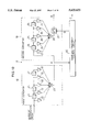
FIG. 1 is a block diagram which shows a main construction of a codec apparatus according to embodiment 1 of the present invention.
FIG. 2 is a drawing which shows a construction of an Fs changing circuit in the codec apparatus.
FIG. 3 is a graph which shows a frequency bandwidth of a signal to be inputted to the codec apparatus when the frequency bandwidth is mostly less than fs /2.
FIG. 4 is a graph which shows the frequency bandwidth of the signal to be inputted to the codec apparatus when the frequency bandwidth is mostly less than fs.
FIG. 5 is a graph which shows the frequency bandwidth of the signal to be inputted to the codec apparatus when the frequency bandwidth is in the proximity of (2×fs).
FIG. 6 is a timing chart when a signal is thinned in the Fs changing circuit; FIG. 6(a) shows that the signal is thinned to 1/4; FIG. 6 (b) shows that the signal is thinned to 1/2; and FIG. 6(c) shows that the signal is not thinned.
FIG. 7 is a drawing which explains one example of a storage region for storing coded data, and data which represent an Fs in the codec apparatus.
FIG. 8 is a drawing which explains another example of the storage region for storing the decoded data and the data which represent the Fs in the codec apparatus.
FIG. 9 is a block diagram which shows a main construction of a codec apparatus according to embodiment 2 of the present invention.
FIG. 10 is a drawing which explains a decimation filter and an Fs control circuit in the codec apparatus.
FIG. 11 is a block diagram which shows the Fs control circuit.
FIG. 12 is a block diagram of a power comparator in the codec apparatus according to the embodiments 1 and 2.
FIG. 13 is a block diagram of a clock divider in the power comparator.
FIGS. 14(a) through 14(f) are timing charts which show a synchronization between a clock signal and a signal D in the clock divider.
DESCRIPTION OF THE EMBODIMENTS
[EMBODIMENT 1]
Referring to FIGS. 1 through 8, the following description will discuss one embodiment of the present invention as EMBODIMENT 1.
A codec apparatus has an A-D converter 1, a sampling frequency (hereinafter, noted as Fs), a changing circuit 2, a coding circuit 3 and a memory 4.
The A-D converter 1 converts an analog signal S to be coded to a digital signal per a predetermined number of bits in accordance with a predetermined first Fs, and outputs the digital signal A to the Fs changing circuit 2.
The first Fs is set based upon the widest frequency bandwidth of an analog signal which is used in the codec apparatus. For example, it can be set to correspond to twice the widest bandwidth.
The Fs changing circuit 2 has an Fs switching circuit (changing means) 5 and an Fs detection circuit (detection means) 6. The Fs detection circuit 6 discriminates the frequency bandwidth of the digital signal, and outputs a control signal D to the Fs switching circuit 5 based upon the detected frequency bandwidth.
The Fs switching circuit 5 outputs either a digital signal B which has been obtained by changing a first Fs of the inputted digital signal A to a second Fs, or the digital signal B still having the first Fs to the coding circuit 3 based upon the control signal D.
The coding circuit 3 performs a compressing process, etc. on the digital signal B from the Fs switching circuit 5, prepares coded data to be stored in the memory 4, and outputs the coded data.
The memory 4 is a magnetic storage medium such as a hard disc, or a random access memory, and has a storage region where the coded data are successively stored. In addition, a data signal C, which is outputted from the Fs detection circuit 6, is inputted and stored in the memory 4. The data signal C is data which discriminates the second Fs of the digital signal from the Fs switching circuit 5.
With the above arrangement, the Fs detection circuit 6 discriminates a frequency bandwidth of the analog signal S, and outputs the bandwidth to the Fs switching circuit 5 as the control signal D. The Fs switching circuit 5 changes the first Fs of the digital signal from the A-D converter 1 to the second Fs in accordance with the control signal D.
In other words, when the bandwidth is narrow, the second Fs is set low. In contrast, when the bandwidth is wide, the second Fs is set high. Further, when the bandwidth is widest, the first Fs is outputted as the second Fs.
Therefore, with this arrangement, it is possible to change the second Fs of the digital signal according to the frequency bandwidth of the analog signal so as to, for example, always becomes twice the bandwidth.
The digital signal B from the Fs switching circuit 5 is inputted to the coding circuit 3, and becomes coded data in the coding circuit 3. The coded data is inputted and stored to memory 4.
Therefore, since this arrangement always makes the second Fs of the digital signal correspond to twice the frequency bandwidth of the analog signal, it is possible to always maintain sound quality of the analog signal which has been decoded from the coded data stored in the memory 4.
Furthermore, this arrangement can prevent the second Fs from being set excessively high.
This reason will be described as follows. Generally, as an Fs of a digital signal becomes higher, the capacity of the storage region in the memory 4 becomes larger. And in order to maintain quality in the decoded analog signal, the Fs of the digital signal should be set so as to become twice the frequency bandwidth of the inputted analog signal.
Therefore, in the conventional manner, in order to accommodate each signal in various bands, a storage region in memory must be sized for a signal having the widest bandwidth. As a result, a portion of that storage region is very likely to go unused unless the widest bandwidth signal is received.
However, with the inventive arrangement, since the Fs of the digital signal is changed according to the frequency bandwidth of the analog signal S to be inputted, the storage region does not have to be preliminarily secured (as previously discussed).
Therefore, this arrangement not only always ensures sound quality, but also makes it possible to reduce the necessary size of the storage region in the memory 4. As a result, it is possible for memory 4 to have a compact design and to be efficiently utilized.
In addition, in the case where a digital signal is coded by the coding circuit 3, it takes more time to code the digital signal in proportion to a higher level of the Fs. Since this arrangement prevents an excessively high Fs, the time it takes to code the digital signal can be reduced. This improves the processing speed for coding the digital signal.
Next, the following description will more concretely discuss the arrangement that a first Fs is changed to a second Fs in the Fs changing circuit 2. The first Fs can be changed to the second Fs, which is used for coding, by thinning an output from the AD converter 1.
As shown in FIG. 2, the Fs changing circuit is provided with a filter 7 which eliminates aliasing noises due to the first Fs from the digital signal A, and a switch (switching means) 8 which thins the output from the filter 7 in a predetermined interval.
For example, an FIR (Finite Impulse Response) type filter is used as the filter 7. The filter 7 is a basic digital filter.
The filter 7 is provided with a plurality of delay units 9 . . . , a plurality of coefficient units 10 . . . and an adder 11. The respective delay units 9 . . . successively delay inputted signals. The respective coefficient units 10 . . . multiply the inputted signals from the respective delay units 9 . . . by coefficients and output the respective signals. The adder 11 adds signals from the respective coefficient units 10 . . . and outputs the added signal. In the filter 7, a desired filter characteristic can be obtained by respectively adjusting the coefficients of the coefficient units 10 . . . .
An AND gate, etc. is used as the switch 8. While maintaining the quality of the digital signal inputted to the Fs changing circuit 2, the filter 7 and the switch 8 change the first Fs of the digital signal A to the second Fs so as to output the digital signal B to the coding circuit 3.
Next, the following description will discuss an operation in the Fs changing circuit 2. First, if a digital signal from the AD converter 1 is inputted at a specified first Fs (here, 4×fs), an operating speed of the filter 7 become 4 times fs. At this time, the adder 11 also outputs the first Fs of (4×fs).
The digital signal, which will be an output of the adder 11, is thinned out per a cycle of Ts and outputted, thereby changing the first Fs to a second Fs. Here, the cycle Ts is equal to 1/(4×fs) which is the reciprocal of the frequency (4×fs).
In other words, in the Fs changing circuit 2, after the digital signal is thinned out by the switch 8, the inputted digital signal A, whose first Fs has been changed to a second Fs, is outputted as the digital signal B.
Next, the following description will discuss in more detail the Fs detection circuit 6 which detects a frequency bandwidth of an analog signal S to be inputted so as to change the Fs of the digital signal inputted to the Fs changing circuit 2, according to the frequency bandwidth.
First, the Fs detection circuit 6 includes two low-pass filters (hereinafter, noted as LPF) 12 and 13 and a power comparator (comparison means) 14. In the LPF 12, a frequency component of, for example, less than fs /2 is extracted from the digital signal A from the A-D converter 1, so as to be outputted. In the LPF 13, a frequency component of, for example, less than Fs is extracted from the digital signal A, so as to be outputted.
The outputs of the LPFs 12 and 13 and the digital signal A are respectively inputted in the power comparator 14, and the powers of the inputs are compared with one another so that the frequency bandwidth of the digital signal from the A-D converter 1 is detected. (The arrangement of the power comparator 14 will be mentioned later.) In this manner, the Fs detection circuit 6 detects the frequency bandwidth of the original analog signal.
In addition, the power comparator 14 outputs the control signal D, which controls the switch 8, to the switch 8 in accordance with the detected bandwidth, and outputs data which discriminate the Fs changed by the control signal D to the memory 4.
In the Fs changing circuit 2, the Fs is controlled as follows. First, as shown in FIG. 3, in the case where an inputted digital signal is an ordinary sound signal whose frequency bandwidth is distributed in a low range, when a ratio of the frequency bandwidth of the digital signal is compared, the bandwidth becomes less than fs /2.
In this case, as shown in FIG. 6(a), in the Fs changing circuit 2, the switch 8 is controlled by the Fs detection circuit 6, which has detected the bandwidth, so as to be turned ON 1/4 time (turned ON during a period of Ts, and turned OFF during the remaining period of 3×Ts).
Thereafter, the signal B is outputted at a second Fs which becomes fs by thinning an output from the filter 7 to 1/4. Therefore, the second Fs becomes fs, namely, becomes twice fs /2 which is the frequency bandwidth of the original analog signal. As a result, the information of the analog signal can be accurately transmitted.
Furthermore, as shown in FIG. 4, in the case where the signal is produced from, for example, simple melodical music having a frequency bandwidth up to a middle range, and the frequency bandwidth is less than Fs, as shown in FIG. 6(b), the switch 8 of FIG. 2 is controlled so as to be turned ON 1/2 time.
In other words, the switch 8 is controlled so as to be ON during a period of Ts, be OFF during the next period of Ts, be ON during the still next period of Ts, and be OFF during the still next period of Ts.
As a result, the output of the digital signal is thinned to 1/2, and the signal is outputted at a second Fs of (2×fs). Since the second Fs becomes (2×fs), that is, becomes twice fs which is equal to the frequency bandwidth of the original analog signal, the information of the analog signal can be accurately transmitted.
Moreover, as shown in FIG. 5, if the signal is produced from, for example, normal music having a frequency bandwidth of up to a high range, and the frequency component is spread in the proximity of (2×fs), as shown in FIG. 6(c), the switch 8 of FIG. 2 is controlled to be always turned ON.
As a result, the digital signal is outputted at a second Fs of (4×fs) without thinning the output of the digital signal. Therefore, since the second Fs becomes (4×fs), that is, twice the frequency bandwidth of the original analog signal, the information of the analog signal can be accurately transmitted.
Here, an ON/OFF control in the switch 8 is operated so as to synchronize with the first Fs of the digital signal inputted in the power comparator 14 as described later.
As mentioned above, with this arrangement, setting of the Fs changing circuit 2 makes it possible to avoid preliminarily setting a storage region (as previously described), as well as to make the memory 4 compact and efficient.
Furthermore, this arrangement reduces a delay of the coding speed in the coding circuit 3 which would occur with an excessively high Fs, thereby improving a processing speed at the time of coding the digital signal B.
Here, with respect to the way to store data which discriminate a second Fs from the Fs switching circuit 5, storage data formats shown in FIGS. 7 and 8 are considered. Such data formats require reducing an amount of data which is added to coded data so as to provide an economical codec apparatus.
The data format which is shown in FIG. 7 is a method for adding Fs data (which represent an Fs) to a head section of coded data. This simple method can provide a simple circuit arrangement, but a data compression rate is lowered and economy of a memory is deteriorated because the Fs data are added to all coded data.
The data format shown in FIG. 8 is a method for adding number data which represent a number in the case where coded data having the same Fs continue. This method is effective when the Fs is not changed frequently.
At this time, in the above method, if the Fs has two variations, as shown in the drawing, only number data which represent a number of coded data which continue with the same Fs, and data which represent the Fs of the first coded data group, are stored.
However, if the Fs has three variations, not only the number data but also discrimination data for discriminating a kind of each Fs are added.
Here, in spite of storing the number data, the storing method is also adaptable for inserting delimiter data into a portion where the Fs is changed.
[EMBODIMENT 2]
Referring to FIGS. 7 through 11, the following description will discuss another embodiment of the present invention as embodiment 2. Here, those members of the present embodiment that have the same arrangement and function, and that are mentioned in the aforementioned embodiment, are indicated by the same reference numerals and description thereof is omitted.
In a codec apparatus of embodiment 2, in spite of the A-D converter 1, as shown in FIG. 9, an A-D converter (conversion means) 15 having an over-sampling mode changes an Fs of a digital signal as described above.
The A-D converter 15 includes a ΔΣ modulation circuit 16 and a decimation filter 17. The decimation filter 17 has a function of converting a higher Fs to a predetermined lower Fs.
Therefore, the A-D converter 15 can change an Fs without separately providing the Fs changing circuit 2 which is shown in FIG. 1.
An over-sampling frequency of the A-D converter 15 is set according to a purpose of a signal which will be subject to an A-D conversion. Normally, the ΔΣ modulation circuit 16 operates in correspondence with a frequency several hundred times a target Fs, and in the A-D converter 15, it is necessary to change the frequency to a normal Fs which is one several hundredths of the frequency. Therefore, the decimation filter 17 includes a first converter 18 and a second converter 19.
As shown in FIG. 10, the first converter 18 has a plurality of delay units 21 . . . , a plurality of coefficient units 22 . . . and an adder 23. In the delay units 21 . . . , output signals from the ΔΣ modulation circuit 16 are successively delayed per a cycle of Ts. In the coefficient units 22 . . . the output signals and the signals from the respective delay units 21 . . . are multiplied by coefficients. In the adder 23, the signals from the respective coefficient units 22 . . . are added to one another and outputted.
Similar to the first converter 18, the second converter 19 has a plurality of delay units 24 . . . and a plurality of coefficient units 25 . . . , an adder 26, and further, a switch (switching member) 27 which is similar to the aforementioned switch 8 and to which a signal is inputted.
In the first converter 18, an output signal from the ΔΣ modulation circuit 16 is received, and an Fs is changed so that it becomes several times that of a target Fs. Then the output signal is output to the second converter 19. Successively, the signal A, which has been converted in the aforementioned manner, is converted in the second converter 19 so as to have the target Fs. Then the signal A is output to the switch 27.
The codec apparatus is provided with an Fs control circuit (control means) 20 for controlling the switch 27. The Fs control circuit 20 observes an output from the first converter 18, detects a frequency bandwidth of the output, and controls an Fs of a digital signal output from the second converter 19 based upon the bandwidth.
Therefore, the Fs control circuit 20 is capable of changing an Fs of a digital signal B to be input to the coding circuit 3 according to the bandwidth, for example changing it so as to become twice the bandwidth. The digital signal B from the second converter 19 is supplied to the aforementioned coding circuit 3. An output from the coding circuit 3 is supplied to the memory 4.
Next, the following description will discuss in more detail the Fs control circuit 20. For example, as shown in FIG. 11, the Fs control circuit 20 is provided with an LPF 28, an LPF 29 and a power comparator 30. Similar to the aforementioned LPF 12, the LPF 28 extracts a frequency bandwidth of the digital signal which is less than fs /2. Similar to the aforementioned LPF 13, the LPF 29 extracts a frequency bandwidth of the digital signal which is less than fs.
The power comparator 30 is capable of detecting a frequency bandwidth in an output of the first converter 18 by comparing the respective outputs from the LPF 28 and the LPF 29, and an output from the first converter 18. A detailed arrangement of the power comparator 30 will be described later.
As mentioned above, a selection is made from, for example, fs, (2×fs) and (4×fs) for an Fs based upon the detected bandwidth. For example, if the bandwidth is mostly less than fs /2, then the Fs is set as fs. If the bandwidth is mostly less than fs, then the Fs is set as (2×fs).
In the Fs control circuit 20, when an optimum Fs is set by comparing the respective outputs with one another, a signal D is provided for controlling the Fs of the digital signal B of the second converter 19. Furthermore, the Fs control circuit 20 outputs a signal C for storing data, which discriminate a current Fs, to the memory 4 in the same manner as embodiment 1. The signal C is stored in the memory 4 in the same manner as embodiment 1 (see FIG. 7 or FIG. 8).
Here, if two kinds of Fs to be inputted to the coding circuit 3 exist, then there should be one LPF.
A signal for controlling the second converter 19, that is similar to the signal for controlling the switch 8 shown in FIG. 2, determines a thinning cycle. At this time, when coefficients of the respective coefficient units 22 . . . and 25 . . . are changed (if necessary), then a signal with less aliasing noise can be obtained.
As to a method for storing the current Fs to the memory 4, the method as described in embodiment 1 is used.
As mentioned in embodiment 2, in the case where the Fs is changed by using the decimation filter 17, accuracy of the signal can be obtained in the decimation filter 17 by converting an over-sampled signal to a predetermined sampling frequency. Therefore, the decimation filter 17 is designed to avoid deterioration in the accuracy of the signal due to a change in the output of the second converter 19.
The above-mentioned description discusses only a coding operation. The following description will discuss a decoding operation. With the arrangements of the respective embodiments, the Fs needed for decoding is definitely stored in the memory 4.
Therefore, for example, if an Fs of the DA converter is set according to the above-mentioned data, then data coded by using the present invention can be accurately decoded. In other words, the Fs of the DA converter is controlled according to data which represent the Fs stored in the memory 4, or data which represent a switching portion of the Fs.
With the arrangements of the respective embodiments, an Fs of an audio signal can be changed to an optimum Fs according to a frequency bandwidth of the original audio signal. As a result, when the audio signal is coded, it is possible to eliminate wasted memory (which occurs in the conventional situation with Fs set excessively high), without deteriorating sound quality of the audio signal.
As mentioned above, with the arrangement of embodiment 2, the memory 4 may have compact design may be efficiently utilized.
Furthermore, this arrangement avoids prolonged coding which would occur due to an excessive Fs, thereby improving the processing speed of a coded digital signal converted from the analog signal.
In addition, with the arrangements of the respective embodiments, a frequency bandwidth of a signal to be coded is always observed, and the Fs of the signal is changed in real time. Therefore, an operator can start a coding operation on an analog signal without considering the type and frequency bandwidth of analog signal to be coded, and can continue the coding operation on the analog signal even if the signal's type or frequency bandwidth changes. As a result, the optimal coding operation for the analog signal can be performed, saving the operator time.
Here, with the arrangement of the present embodiment, the description has discussed examples where coded data are stored in the memory 4. However, it is obvious that this arrangement is also adaptable to cases in which coded data are transmitted by other means such as optical fiber or radio.
Next, the following description will discuss power comparators 14 and 30 in detail. Since the power comparators 14 and 30 have the same function, the following description will discuss only power comparator 14.
As shown in FIG. 12, the power comparator 14 has three multipliers 31, 32 and 33, two OP amplifiers 34 and 35, two judging units 36 and 37, and a clock divider 38. Digital signals of respective frequency bandwidths are respectively inputted to the multipliers 31, 32 and 33. The respective frequency bandwidths are fs /2 or less, fs or less, and whole bandwidth.
The respective multipliers 31, 32 and 33 square the inputted digital signals so that the digital signals become positive, and output the digital signals representing power in each frequency bandwidth.
The output of the multiplier 31 is input to a minus side of the OP amplifier 34, which acts as a comparator. The output of the multiplier 32 is input to a plus side of the OP amplifier 34 and to a minus side of the OP amplifier 35. The output of the multiplier 33 is input to a plus side of the OP amplifier 35.
As a result, the OP amplifier 34 compares a signal of fs /2 or less with a signal of fs or less. When the power of the signal of (fs /2 or less) is smaller than the power of the signal of (fs or less), the OP amplifier 34 outputs a positive signal in proportion to the difference between both powers, and when both powers are equal, outputs a zero signal.
Meanwhile, the OP amplifier 35 compares a signal of fs or less with a signal of whole bandwidth. When the power of the signal of (fs or less) is smaller than the power of the signal of whole bandwidth, the OP amplifier 35 outputs a positive signal in proportion to the difference between both powers, and when both powers are equal, outputs a zero signal.
The output of the OP amplifier 34 is input to the judging unit 36. The judging unit 36 judges the amount of the output and outputs the judged signal as C2. In other words, when the output of OP amplifier 34 is larger than a prescribed value, the judging unit 36 outputs a signal "1" representing an "H" level, and when the output is smaller than the prescribed value, outputs a signal "0" representing an "L" level.
In contrast, the output of the OP amplifier 35 is supplied to the judging unit 37. The judging unit 37 judges the amount of the output and outputs the judged signal as C1. When the output is larger than a prescribed value, the judging unit 37 outputs the signal "1" representing the "H" level, and when the output is smaller than the prescribed value, outputs the signal "0" representing the "L" level.
Here, a signal to be outputted from the power comparator 14 to the memory 4 is represented as one signal C. However, in the case where respective three frequency bandwidths are set as mentioned above, the signal C requires two signals C2 and C1.
The respective signals C2 and C1 are also input to the clock divider 38. The clock signal (4×fs) has been input to the clock divider 38. As shown in FIG. 13, clock divider 38 is provided with a NOR circuit 39 receiving respective signals from C2 and C1, as well as an AND circuit 41 receiving the signal C2 and a signal obtained by converting C1 by means of the inverter 40.
The clock divider 38 to which the clock signal (4×fs) (see FIG. 14(a)) is inputted is provided with a flip flop 42 for halving the clock signal to a frequency of (2×fs) (see FIG. 14 (b)). In flip flop 42, the clock signal is input to a clock input of the flip flop 42, and an inversion output Q-bar in the flip flop 42 is input to a data input D in the flip flop 42.
A flip flop 43 halves the (2×fs) signal to fs (see FIG. 14 (c)). The output Q-bar from flip flop 42 is input to a clock input in the flip flop 43, and an inversion output Q-bar of the flip flop 43 is input to a data input D in the flip flop 43.
An AND circuit 44 receives the inversion output Q-bars from the flip flops 42 and 43. A switch 45 receives the output of the AND circuit 44 so as to switch the output in accordance with the signal from the NOR circuit 39.
A switch 46 receives the inversion output Q-bar of the flip flop 42 so as to switch the output in accordance with the signal from the AND circuit 41. A switch 47 receives a source voltage so as to switch the source voltage in accordance with the signal from the signal C1.
The respective switches 45, 46 and 47 are set so as to be turned ON when each inputted signal is at the "H" level, and turned OFF when each inputted signal is at the "L" level. Furthermore, the source voltage represents a voltage when each signal is at the "H" level.
Next, the operation of the power comparator 14 is discussed. First, when the digital signal A obtained by digitizing the analog signal S having a frequency bandwidth of (fs /2 or less) is inputted to the Fs detection circuit 6, a first signal of only fs /2 or less and a second signal of only fs or less are produced from the digital signal A by the LPFs 12 and 13 of the Fs detection circuit 6.
The first signal, the second signal, and the digital signal A are supplied to power comparator The signals are respectively input to the multipliers 31, 32 and 33, and powers of the signals are detected. The powers of the first and second signals are supplied to the OP amplifier 34 for comparison.
At this time, since the original analog signal S has a frequency bandwidth of (fs /2 or less), the powers substantially become equal. Therefore, since the output of the OP amplifier 34 substantially becomes zero, the judging unit 36 outputs a signal of the "L" level as signal C2. Meanwhile, the other judging unit 37 similarly outputs a signal of the "L" level as signal C1.
In this way, when both of signals C1 and C2 become the "L" level, the output of NOR circuit 39 becomes the "H" level and the switch 45 which is controlled in accordance with that output is turned ON in the clock divider 38 where each signal has been inputted. In contrast, when both of signals C1 and C2 become the "L" level, the output of the AND circuit 41 becomes the "L" level, and the switch 46 is turned OFF. Further, since the signal C1 is also at the "L" level, the switch 47 is turned OFF.
Therefore, after being synchronized with the first transition of the clock signal, the signal D which is equal to the output of the switch 45 becomes the "H" level for one pulse of the clock signal, and becomes the "L" level for the subsequent three pulses of the clock signal. Thereafter, this cycle (see FIG. 14(e)) is repeated. Here, L shown in the drawing represents the "L" level.
In the case where the original analog signal S has a frequency bandwidth of fs or less, as shown in FIGS. 12 and 13, the output signal C1 becomes the "L" level, and the output of the signal C2 becomes the "H" level. As a result, since the output of the AND circuit 41 becomes the "H" level, only the switch 46 is turned ON.
Therefore, as shown in FIG. 14, after being synchronized with the first transition of the clock signal, the signal D which is equal to the output of the switch 46 becomes the "H" level for one pulse of the clock signal, and becomes "L" level for the following one pulse of the clock signal. Thereafter, this cycle (See FIG. 14(d)) is repeated.
In the case where the original analog signal S has a whole bandwidth, the output of the signal C1 becomes the "H" level, and the output of the signal C2 becomes the "H" level or the "L" level. As a result, since the output of the signal C1 becomes the "H" level, only the switch 47 is turned ON. Therefore, the signal D which is equal to the output of the switch 47 is always at the "H" level (see FIG. 14(f)).
With each arrangement of the above embodiments, the power comparator 14 can switch the switch 8 in synch with the clock signal, and can thin the digital signal A inputted to the Fs changing circuit 5 in synch with the clock signal.
The invention being thus described, it will be obvious that the same may be varied in many ways. Such variations are not to be regarded as a departure from the spirit and scope of the invention, and all such modifications as would be obvious to one skilled in the art are intended to be included within the scope of the following claims.