US5610094A - Photoelectric conversion device - Google Patents

Photoelectric conversion device Download PDF

Info

Publication number
US5610094A
US5610094A US08/475,830 US47583095A US5610094A US 5610094 A US5610094 A US 5610094A US 47583095 A US47583095 A US 47583095A US 5610094 A US5610094 A US 5610094A
Authority
US
United States
Prior art keywords
layer
forming
nucleation
nucleus
substrate
Prior art date
Legal status (The legal status is an assumption and is not a legal conclusion. Google has not performed a legal analysis and makes no representation as to the accuracy of the status listed.)
Expired - Fee Related
Application number
US08/475,830
Inventor
Masaharu Ozaki
Takao Yonehara
Current Assignee (The listed assignees may be inaccurate. Google has not performed a legal analysis and makes no representation or warranty as to the accuracy of the list.)
Canon Inc
Original Assignee
Canon Inc
Priority date (The priority date is an assumption and is not a legal conclusion. Google has not performed a legal analysis and makes no representation as to the accuracy of the date listed.)
Filing date
Publication date
Application filed by Canon Inc filed Critical Canon Inc
Priority to US08/475,830 priority Critical patent/US5610094A/en
Application granted granted Critical
Publication of US5610094A publication Critical patent/US5610094A/en
Anticipated expiration legal-status Critical
Expired - Fee Related legal-status Critical Current

Links

Images

Classifications

    • HELECTRICITY
    • H01ELECTRIC ELEMENTS
    • H01LSEMICONDUCTOR DEVICES NOT COVERED BY CLASS H10
    • H01L27/00Devices consisting of a plurality of semiconductor or other solid-state components formed in or on a common substrate
    • H01L27/02Devices consisting of a plurality of semiconductor or other solid-state components formed in or on a common substrate including semiconductor components specially adapted for rectifying, oscillating, amplifying or switching and having at least one potential-jump barrier or surface barrier; including integrated passive circuit elements with at least one potential-jump barrier or surface barrier
    • H01L27/04Devices consisting of a plurality of semiconductor or other solid-state components formed in or on a common substrate including semiconductor components specially adapted for rectifying, oscillating, amplifying or switching and having at least one potential-jump barrier or surface barrier; including integrated passive circuit elements with at least one potential-jump barrier or surface barrier the substrate being a semiconductor body
    • H01L27/06Devices consisting of a plurality of semiconductor or other solid-state components formed in or on a common substrate including semiconductor components specially adapted for rectifying, oscillating, amplifying or switching and having at least one potential-jump barrier or surface barrier; including integrated passive circuit elements with at least one potential-jump barrier or surface barrier the substrate being a semiconductor body including a plurality of individual components in a non-repetitive configuration
    • H01L27/0688Integrated circuits having a three-dimensional layout
    • CCHEMISTRY; METALLURGY
    • C30CRYSTAL GROWTH
    • C30BSINGLE-CRYSTAL GROWTH; UNIDIRECTIONAL SOLIDIFICATION OF EUTECTIC MATERIAL OR UNIDIRECTIONAL DEMIXING OF EUTECTOID MATERIAL; REFINING BY ZONE-MELTING OF MATERIAL; PRODUCTION OF A HOMOGENEOUS POLYCRYSTALLINE MATERIAL WITH DEFINED STRUCTURE; SINGLE CRYSTALS OR HOMOGENEOUS POLYCRYSTALLINE MATERIAL WITH DEFINED STRUCTURE; AFTER-TREATMENT OF SINGLE CRYSTALS OR A HOMOGENEOUS POLYCRYSTALLINE MATERIAL WITH DEFINED STRUCTURE; APPARATUS THEREFOR
    • C30B23/00Single-crystal growth by condensing evaporated or sublimed materials
    • C30B23/02Epitaxial-layer growth
    • C30B23/04Pattern deposit, e.g. by using masks
    • CCHEMISTRY; METALLURGY
    • C30CRYSTAL GROWTH
    • C30BSINGLE-CRYSTAL GROWTH; UNIDIRECTIONAL SOLIDIFICATION OF EUTECTIC MATERIAL OR UNIDIRECTIONAL DEMIXING OF EUTECTOID MATERIAL; REFINING BY ZONE-MELTING OF MATERIAL; PRODUCTION OF A HOMOGENEOUS POLYCRYSTALLINE MATERIAL WITH DEFINED STRUCTURE; SINGLE CRYSTALS OR HOMOGENEOUS POLYCRYSTALLINE MATERIAL WITH DEFINED STRUCTURE; AFTER-TREATMENT OF SINGLE CRYSTALS OR A HOMOGENEOUS POLYCRYSTALLINE MATERIAL WITH DEFINED STRUCTURE; APPARATUS THEREFOR
    • C30B25/00Single-crystal growth by chemical reaction of reactive gases, e.g. chemical vapour-deposition growth
    • C30B25/02Epitaxial-layer growth
    • C30B25/18Epitaxial-layer growth characterised by the substrate
    • HELECTRICITY
    • H01ELECTRIC ELEMENTS
    • H01LSEMICONDUCTOR DEVICES NOT COVERED BY CLASS H10
    • H01L21/00Processes or apparatus adapted for the manufacture or treatment of semiconductor or solid state devices or of parts thereof
    • H01L21/02Manufacture or treatment of semiconductor devices or of parts thereof
    • H01L21/02104Forming layers
    • H01L21/02365Forming inorganic semiconducting materials on a substrate
    • H01L21/02367Substrates
    • H01L21/0237Materials
    • H01L21/02373Group 14 semiconducting materials
    • H01L21/02381Silicon, silicon germanium, germanium
    • HELECTRICITY
    • H01ELECTRIC ELEMENTS
    • H01LSEMICONDUCTOR DEVICES NOT COVERED BY CLASS H10
    • H01L21/00Processes or apparatus adapted for the manufacture or treatment of semiconductor or solid state devices or of parts thereof
    • H01L21/02Manufacture or treatment of semiconductor devices or of parts thereof
    • H01L21/02104Forming layers
    • H01L21/02365Forming inorganic semiconducting materials on a substrate
    • H01L21/02367Substrates
    • H01L21/0237Materials
    • H01L21/02387Group 13/15 materials
    • H01L21/02395Arsenides
    • HELECTRICITY
    • H01ELECTRIC ELEMENTS
    • H01LSEMICONDUCTOR DEVICES NOT COVERED BY CLASS H10
    • H01L21/00Processes or apparatus adapted for the manufacture or treatment of semiconductor or solid state devices or of parts thereof
    • H01L21/02Manufacture or treatment of semiconductor devices or of parts thereof
    • H01L21/02104Forming layers
    • H01L21/02365Forming inorganic semiconducting materials on a substrate
    • H01L21/02367Substrates
    • H01L21/0237Materials
    • H01L21/0242Crystalline insulating materials
    • HELECTRICITY
    • H01ELECTRIC ELEMENTS
    • H01LSEMICONDUCTOR DEVICES NOT COVERED BY CLASS H10
    • H01L21/00Processes or apparatus adapted for the manufacture or treatment of semiconductor or solid state devices or of parts thereof
    • H01L21/02Manufacture or treatment of semiconductor devices or of parts thereof
    • H01L21/02104Forming layers
    • H01L21/02365Forming inorganic semiconducting materials on a substrate
    • H01L21/02518Deposited layers
    • H01L21/02521Materials
    • H01L21/02524Group 14 semiconducting materials
    • H01L21/02532Silicon, silicon germanium, germanium
    • HELECTRICITY
    • H01ELECTRIC ELEMENTS
    • H01LSEMICONDUCTOR DEVICES NOT COVERED BY CLASS H10
    • H01L21/00Processes or apparatus adapted for the manufacture or treatment of semiconductor or solid state devices or of parts thereof
    • H01L21/02Manufacture or treatment of semiconductor devices or of parts thereof
    • H01L21/02104Forming layers
    • H01L21/02365Forming inorganic semiconducting materials on a substrate
    • H01L21/02612Formation types
    • H01L21/02617Deposition types
    • H01L21/0262Reduction or decomposition of gaseous compounds, e.g. CVD
    • HELECTRICITY
    • H01ELECTRIC ELEMENTS
    • H01LSEMICONDUCTOR DEVICES NOT COVERED BY CLASS H10
    • H01L21/00Processes or apparatus adapted for the manufacture or treatment of semiconductor or solid state devices or of parts thereof
    • H01L21/02Manufacture or treatment of semiconductor devices or of parts thereof
    • H01L21/02104Forming layers
    • H01L21/02365Forming inorganic semiconducting materials on a substrate
    • H01L21/02612Formation types
    • H01L21/02617Deposition types
    • H01L21/02636Selective deposition, e.g. simultaneous growth of mono- and non-monocrystalline semiconductor materials
    • H01L21/02639Preparation of substrate for selective deposition
    • H01L21/02645Seed materials
    • HELECTRICITY
    • H01ELECTRIC ELEMENTS
    • H01LSEMICONDUCTOR DEVICES NOT COVERED BY CLASS H10
    • H01L21/00Processes or apparatus adapted for the manufacture or treatment of semiconductor or solid state devices or of parts thereof
    • H01L21/02Manufacture or treatment of semiconductor devices or of parts thereof
    • H01L21/02104Forming layers
    • H01L21/02365Forming inorganic semiconducting materials on a substrate
    • H01L21/02612Formation types
    • H01L21/02617Deposition types
    • H01L21/02636Selective deposition, e.g. simultaneous growth of mono- and non-monocrystalline semiconductor materials
    • H01L21/02647Lateral overgrowth
    • HELECTRICITY
    • H01ELECTRIC ELEMENTS
    • H01LSEMICONDUCTOR DEVICES NOT COVERED BY CLASS H10
    • H01L27/00Devices consisting of a plurality of semiconductor or other solid-state components formed in or on a common substrate
    • H01L27/14Devices consisting of a plurality of semiconductor or other solid-state components formed in or on a common substrate including semiconductor components sensitive to infrared radiation, light, electromagnetic radiation of shorter wavelength or corpuscular radiation and specially adapted either for the conversion of the energy of such radiation into electrical energy or for the control of electrical energy by such radiation
    • H01L27/144Devices controlled by radiation
    • H01L27/1446Devices controlled by radiation in a repetitive configuration
    • HELECTRICITY
    • H01ELECTRIC ELEMENTS
    • H01LSEMICONDUCTOR DEVICES NOT COVERED BY CLASS H10
    • H01L31/00Semiconductor devices sensitive to infrared radiation, light, electromagnetic radiation of shorter wavelength or corpuscular radiation and specially adapted either for the conversion of the energy of such radiation into electrical energy or for the control of electrical energy by such radiation; Processes or apparatus specially adapted for the manufacture or treatment thereof or of parts thereof; Details thereof
    • H01L31/0248Semiconductor devices sensitive to infrared radiation, light, electromagnetic radiation of shorter wavelength or corpuscular radiation and specially adapted either for the conversion of the energy of such radiation into electrical energy or for the control of electrical energy by such radiation; Processes or apparatus specially adapted for the manufacture or treatment thereof or of parts thereof; Details thereof characterised by their semiconductor bodies
    • H01L31/036Semiconductor devices sensitive to infrared radiation, light, electromagnetic radiation of shorter wavelength or corpuscular radiation and specially adapted either for the conversion of the energy of such radiation into electrical energy or for the control of electrical energy by such radiation; Processes or apparatus specially adapted for the manufacture or treatment thereof or of parts thereof; Details thereof characterised by their semiconductor bodies characterised by their crystalline structure or particular orientation of the crystalline planes
    • H01L31/0368Semiconductor devices sensitive to infrared radiation, light, electromagnetic radiation of shorter wavelength or corpuscular radiation and specially adapted either for the conversion of the energy of such radiation into electrical energy or for the control of electrical energy by such radiation; Processes or apparatus specially adapted for the manufacture or treatment thereof or of parts thereof; Details thereof characterised by their semiconductor bodies characterised by their crystalline structure or particular orientation of the crystalline planes including polycrystalline semiconductors
    • HELECTRICITY
    • H01ELECTRIC ELEMENTS
    • H01LSEMICONDUCTOR DEVICES NOT COVERED BY CLASS H10
    • H01L31/00Semiconductor devices sensitive to infrared radiation, light, electromagnetic radiation of shorter wavelength or corpuscular radiation and specially adapted either for the conversion of the energy of such radiation into electrical energy or for the control of electrical energy by such radiation; Processes or apparatus specially adapted for the manufacture or treatment thereof or of parts thereof; Details thereof
    • H01L31/0248Semiconductor devices sensitive to infrared radiation, light, electromagnetic radiation of shorter wavelength or corpuscular radiation and specially adapted either for the conversion of the energy of such radiation into electrical energy or for the control of electrical energy by such radiation; Processes or apparatus specially adapted for the manufacture or treatment thereof or of parts thereof; Details thereof characterised by their semiconductor bodies
    • H01L31/036Semiconductor devices sensitive to infrared radiation, light, electromagnetic radiation of shorter wavelength or corpuscular radiation and specially adapted either for the conversion of the energy of such radiation into electrical energy or for the control of electrical energy by such radiation; Processes or apparatus specially adapted for the manufacture or treatment thereof or of parts thereof; Details thereof characterised by their semiconductor bodies characterised by their crystalline structure or particular orientation of the crystalline planes
    • H01L31/0376Semiconductor devices sensitive to infrared radiation, light, electromagnetic radiation of shorter wavelength or corpuscular radiation and specially adapted either for the conversion of the energy of such radiation into electrical energy or for the control of electrical energy by such radiation; Processes or apparatus specially adapted for the manufacture or treatment thereof or of parts thereof; Details thereof characterised by their semiconductor bodies characterised by their crystalline structure or particular orientation of the crystalline planes including amorphous semiconductors
    • HELECTRICITY
    • H01ELECTRIC ELEMENTS
    • H01LSEMICONDUCTOR DEVICES NOT COVERED BY CLASS H10
    • H01L31/00Semiconductor devices sensitive to infrared radiation, light, electromagnetic radiation of shorter wavelength or corpuscular radiation and specially adapted either for the conversion of the energy of such radiation into electrical energy or for the control of electrical energy by such radiation; Processes or apparatus specially adapted for the manufacture or treatment thereof or of parts thereof; Details thereof
    • H01L31/18Processes or apparatus specially adapted for the manufacture or treatment of these devices or of parts thereof
    • H01L31/20Processes or apparatus specially adapted for the manufacture or treatment of these devices or of parts thereof such devices or parts thereof comprising amorphous semiconductor materials
    • H01L31/206Particular processes or apparatus for continuous treatment of the devices, e.g. roll-to roll processes, multi-chamber deposition
    • YGENERAL TAGGING OF NEW TECHNOLOGICAL DEVELOPMENTS; GENERAL TAGGING OF CROSS-SECTIONAL TECHNOLOGIES SPANNING OVER SEVERAL SECTIONS OF THE IPC; TECHNICAL SUBJECTS COVERED BY FORMER USPC CROSS-REFERENCE ART COLLECTIONS [XRACs] AND DIGESTS
    • Y02TECHNOLOGIES OR APPLICATIONS FOR MITIGATION OR ADAPTATION AGAINST CLIMATE CHANGE
    • Y02EREDUCTION OF GREENHOUSE GAS [GHG] EMISSIONS, RELATED TO ENERGY GENERATION, TRANSMISSION OR DISTRIBUTION
    • Y02E10/00Energy generation through renewable energy sources
    • Y02E10/50Photovoltaic [PV] energy
    • YGENERAL TAGGING OF NEW TECHNOLOGICAL DEVELOPMENTS; GENERAL TAGGING OF CROSS-SECTIONAL TECHNOLOGIES SPANNING OVER SEVERAL SECTIONS OF THE IPC; TECHNICAL SUBJECTS COVERED BY FORMER USPC CROSS-REFERENCE ART COLLECTIONS [XRACs] AND DIGESTS
    • Y02TECHNOLOGIES OR APPLICATIONS FOR MITIGATION OR ADAPTATION AGAINST CLIMATE CHANGE
    • Y02PCLIMATE CHANGE MITIGATION TECHNOLOGIES IN THE PRODUCTION OR PROCESSING OF GOODS
    • Y02P70/00Climate change mitigation technologies in the production process for final industrial or consumer products
    • Y02P70/50Manufacturing or production processes characterised by the final manufactured product
    • YGENERAL TAGGING OF NEW TECHNOLOGICAL DEVELOPMENTS; GENERAL TAGGING OF CROSS-SECTIONAL TECHNOLOGIES SPANNING OVER SEVERAL SECTIONS OF THE IPC; TECHNICAL SUBJECTS COVERED BY FORMER USPC CROSS-REFERENCE ART COLLECTIONS [XRACs] AND DIGESTS
    • Y10TECHNICAL SUBJECTS COVERED BY FORMER USPC
    • Y10STECHNICAL SUBJECTS COVERED BY FORMER USPC CROSS-REFERENCE ART COLLECTIONS [XRACs] AND DIGESTS
    • Y10S148/00Metal treatment
    • Y10S148/152Single crystal on amorphous substrate
    • YGENERAL TAGGING OF NEW TECHNOLOGICAL DEVELOPMENTS; GENERAL TAGGING OF CROSS-SECTIONAL TECHNOLOGIES SPANNING OVER SEVERAL SECTIONS OF THE IPC; TECHNICAL SUBJECTS COVERED BY FORMER USPC CROSS-REFERENCE ART COLLECTIONS [XRACs] AND DIGESTS
    • Y10TECHNICAL SUBJECTS COVERED BY FORMER USPC
    • Y10STECHNICAL SUBJECTS COVERED BY FORMER USPC CROSS-REFERENCE ART COLLECTIONS [XRACs] AND DIGESTS
    • Y10S148/00Metal treatment
    • Y10S148/164Three dimensional processing

Definitions

  • the present invention relates to a photoelectric conversion device formed by using a crystal layer which is formed by a crystal growth method for selectively growing a crystal with the aid of a difference of nucleation densities between a deposition film forming material and a surface material on which a deposition film is formed.
  • amorphous insulator To fabricate a three-dimensional integrated circuit, it is necessary to form on an amorphous insulator a semiconductor thin film in which electronic elements such as transistors are formed.
  • electronic elements such as transistors are formed.
  • amorphous silicon or polysilicon can grow on an amorphous material.
  • amorphous silicon or polysilicon have been used heretofore as a semiconductor layer for electronic elements, or alternatively monocrystalline silicon has been used which is formed by melting and monocrystallizing grown amorphous silicon or polysilicon with a laser beam.
  • amorphous silicon or polysilicon as a semiconductor layer for electronic elements, however, results in a low electron mobility: lower than 0.1 cm 2 /V sec for amorphous silicon and 1 to 10 cm 2 /V sec for polysilicon having a grain diameter of several hundreds angstroms.
  • a large leakage current flows through a PN junction.
  • electronic elements having a good performance cannot be realized.
  • a monocrystalline silicon layer is used as a semiconductor layer in the method of melting and monocrystallizing the amorphous silicon or polysilicon, electronic elements of good performance can be realized.
  • heating and melting with a laser beam greatly influence the performance of elements formed in an under layer.
  • FIG. 1 is a graph for illustration of the relationship between the size of nucleus, rc and free energy, G, in the process of forming a thin film;
  • FIG. 3 is a graph showing the change with lapse of time of nucleation density (ND) on the deposition surface of SiO 2 and ON the deposition surface of silicon nitride;
  • FIGS. 4A to 4D are illustrations of the formation steps showing a first embodiment of the method for forming a crystal relating to the present invention
  • FIGS. 5A and 5B are perspective views of the substrate in FIGS. 4A and 4D;
  • FIGS. 6A to 6D are illustrations of the formation steps showing a second embodiment of the method for forming a single crystal relating to the present invention.
  • FIGS. 7A and 7B are perspective views of the substrates in FIGS. 6A and 6D;
  • FIGS. 8A to 8D are illustrations of the steps for forming a crystal showing a third embodiment of the method for forming a crystal relating to the present invention.
  • FIGS. 9A to 9C are illustrations of formation steps showing a fourth embodiment of the method for forming a crystal relating to the present invention.
  • FIGS. 10A to 10B are perspective views of the substrates shown in FIGS. 9A and 9C;
  • FIGS. 11A to 11C are illustrations of the steps for forming a crystal showing a fifth embodiment of the method for forming a crystal relating to the present invention.
  • FIGS. 12A to 12D are illustrations of the steps for forming a crystal showing an sixth embodiment of the method for forming a crystal relating to the present invention
  • FIG. 13 is a graph showing the relationship between the flow rate of SiH 4 and NH 3 and the composition ratio of Si and N in the silicon nitride film formed;
  • FIG. 14 is a graph showing the relationship between Si/N composition ratio and nucleation density
  • FIG. 15 is a graph showing the relationship between the injected amount of Si ions and nucleation density
  • FIG. 16 is a sectional view showing an embodiment of the photoelectric conversion device according to the present invention.
  • FIG. 17 is a circuit diagram of the embodiment.
  • a nucleus with a size exceeding rc is called a stable nucleus, and unless otherwise particularly noted, “nucleus” in the following detailed description of the present invention refers to this "stable nucleus". Also, among “stable nucleus”, those with small r are called an "initial nucleus".
  • ⁇ o surface energy between the nucleus and a vacuum.
  • FIG. 1 shows the manner in which G is changed.
  • the radius of curvature of the stable nucleus when G is at the maximum value is rc.
  • nuclei grow to become shaped in islands, and further grow whereby mutual contact between islands progresses until sometimes coalescence occurs and via a network structure, it becomes finally a continuous film to completely cover the substrate surface. Following such a process, a thin film is deposited on the substrate.
  • the density of the nucleus formed per unit area of the substrate surface, the size of nucleus, and the nucleation speed are determined by the state of the system of deposition, and particularly by the interaction between the flying atoms and the substrate surface material.
  • a specific crystal direction grows in parallel to the substrate due to anisotropy relative to the crystal surface of the interface energy at the interface between the deposited material and the substrate, and when the substrate is amorphous, the crystal direction within the substrate plane is not constant.
  • grain boundaries are formed by mutual collision between nuclei or islands, and particularly in the case of mutual collision between islands with some sizes or greater, instead of coalescing grain boundaries are formed. Since the grain boundaries formed are difficulty to move in the solid phase, the grain sizes are determined at that point.
  • the selective deposition method is a method in which a thin film is formed selectively on the substrate by utilizing the differences between the materials and factors influencing nucleus formation in the thin film forming process, such as surface energy, attachment coefficient, release coefficient, surface diffusion speed, etc.
  • SiO 2 may be used as the substrate 1, Si, GaAs, silicon nitride as the thin film 2 and Si, W, GaAs, InP, etc., as the thin film 3 to be deposited.
  • FIG. 3 is a graph showing the change with lapse of time of nucleation density on the deposited surface of SiO 2 and the deposited surface of silicon nitride.
  • nucleation on SiO 2 poses substantially no problem, but by addition of HCl gas into the reaction gas, nucleation on SiO 2 can be further suppressed to make deposition of Si on SiO 2 perfectly zero.
  • Such a phenomenon depends greatly on the difference in adsorption coefficient, release coefficient, surface diffusion coefficient, etc., relative to Si of the material surfaces of SiO 2 and silicon nitride, but the fact that SiO 2 itself is etched by the reaction of SiO 2 with Si atom itself to form silicon monooxide with a higher vapor pressure, while no such etching phenomenon occurs on silicon nitride may be also considered to be a cause to effect selective deposition (T. Yonehara, S. Yoshioka, S. Miyazawa, Journal of Applied Physics 53, 6839, 1982).
  • SiO 2 and silicon nitride as the materials of the deposition surface and silicon as the material to be deposited, a sufficiently great nucleation density difference as shown in the same graph can be obtained.
  • SiO 2 is desirable as the material for the deposition surface, this is not limiting and a sufficiently practical nucleation density difference can be obtained even by use of SiO x (0 ⁇ x ⁇ 2).
  • nucleation density may be sufficiently 10 3 -fold or more in density of nuclei as shown by the same graph, and sufficient selective formation of deposited film can be done with the materials as exemplified below.
  • ions of Si or N may be injected locally into the SiO 2 surface to form a region having excessive Si or N.
  • the present invention utilizes selective deposition based on such nucleation density difference ( ⁇ ND) and, by being formed sufficiently small so that a single nucleus may grow on the deposition surface of a different kind of material having sufficiently greater nucleation density than the material of the deposition surface, a single crystal can be grown selectively only at the site where such small different kind of material exists.
  • ⁇ ND nucleation density difference
  • FIGS. 4A to 4D are illustrations of the formation steps showing a first embodiment of the method for forming a crystal relating to the present invention
  • FIGS. 5A and 5B are perspective views of the substrates in FIGS. 4A and 4D.
  • a thin film 5 [deposition surface (S NDS )] with small nucleation density which enables selective deposition is formed and a material different from the material forming the thin film 5 with greater nucleation density is deposited thinly, followed by patterning according to lithography, etc., to form a sufficiently small deposition surface 6 (S NDL ) (or called "Seed”) comprising a different kind of material.
  • S NDL sufficiently small deposition surface 6
  • the island-shaped single crystal grain 7 further grows while maintaining the single crystal structure with the deposition surface (S NDL ) 6 as the center (lateral overgrowth), whereby it can cover over the whole thin film 5 as shown in FIG. 4C (single crystal 7A).
  • the single crystal 7A is flattened by etching or polishing, and a single S crystal layer 8 capable of forming a desired device can be formed on the thin film 5 as shown in FIG. 4D and FIG. 5B.
  • any desired material can be used for the substrate 4 which is the supporting member. Further, in such a case, even when the substrate 4 may be one having a functional device, etc., formed thereon according to conventional semiconductor technique, the single crystal layer 8 can be easily formed thereon.
  • the nonnucleation surface (S NDS ) is formed of thin film 5, but a substrate comprising a material with small nucleation density (ND) enabling selective nucleation may be used as such and nucleation surfaces (S NDL ) may be provided at any desired positions to form single crystal layers similarly thereon.
  • ND small nucleation density
  • FIGS. 6A-6D are illustrations of the formation steps showing a second embodiment of the method for forming a crystal relating to the present invention
  • FIGS. 7A and 7B are perspective views of the substrates in FIGS. 6A and 6D.
  • nucleation surfaces (S NDL ) 12-1, 12-2 of a material different from the substrate 11 enabling the above selective nucleation are arranged to be sufficiently small.
  • the distance l is set equal to the size of the single crystal region required for formation of semiconductor device or group of devices or greater.
  • the nucleation surfaces (S NDL ) 12-1, 12-2 are required to be formed to a sufficiently small size (area) to the extent that only a single nucleus may be formed.
  • the size of the nucleation surfaces (S NDL ) 12-1, 12-2, which may be different depending on the kind of the material, may be several microns or less.
  • the nucleus grows while maintaining the single crystal structure, and become island-shaped single crystal grains 13-1, 13-2 as shown in FIG. 6B.
  • the crystal direction in the normal line direction of the substrate 11 of the island-shaped single crystal grains 13-1, 13-2 is determined so as to make the interface energy of the material of the substrate 11 and the material forming nucleus a minimum.
  • the surface or interface energy has anisotropy depending on the crystal face.
  • the crystal direction within the substrate plane in amorphous substrate is not determined.
  • the island-shaped single crystal grains 13-1, 13-2 further grow to become single crystals 13A-1, 13A-2 until the adjacent single crystals 13A-1, 13A-2 contact each other as shown in FIG. 6C, but since the crystal direction within the substrate plane is not constant, a crystal grain boundary 14 is formed at the intermediate position between the nucleation surfaces (S NDL ) 12-1 and 12-2.
  • the single crystals 13A-1, 13A-2 grow three-dimensionally, but crystal faces with slow growth speed appear. For this reason, the surfaces of single crystals 13A-1, 13A-2 are flattened by etching or polishing, and further the portion of the grain boundary 14 is removed to form thin films of single crystals 15-1, 15-2 containing no grain boundary in the shape of lattices as shown in FIG. 6D and FIG. 7B.
  • the size of the single crystal films 15-1, 15-2, 15 is determined by the interval l between the nucleation surfaces (S NDL ) as described above. That is, by determining appropriately the formation pattern of the nucleation surface (S NDL ) 12, the position of the grain boundary can be controlled to form single crystals with desired sizes at a desired arrangement.
  • FIGS. 8A-8D are illustration of the steps for forming crystal showing a third embodiment of the method for forming the crystal relating to the present invention.
  • a nonnucleation surface (S NDS ) 5 shaped in a thin film, comprising a material with small nucleation density (ND) enabling selective nucleation is formed on a desired substrate 4, and a nucleation surfaces (S NDL ) 12 comprising a different material with greater nucleation density (ND) are formed at intervals of l thereon, whereby single crystal layers 15 can be formed similarly as in the above third embodiment.
  • S NDS nonnucleation surface
  • S NDL nucleation surfaces
  • FIGS. 9A-9C are illustrations of the formation steps showing a fourth embodiment of the method for forming the crystal relating to the present invention
  • FIGS. 10A and 10B are perspective views of the substrates in FIGS. 9A and 9C.
  • concavities 16 with desired size and shape are formed on the amorphous insulating substrate 11, and nucleation surfaces (S NDL ) 12 with a sufficiently small size for forming only a single nucleus therein.
  • island-shaped single crystal grains 13 are grown similarly as in the first embodiment.
  • single crystal grains 13 are grown until embedding the concavity 16 to form a single crystal layer 17.
  • FIGS. 11A-11C are steps for forming a crystal of a fifth embodiment of the present invention.
  • a nonnucleation surface (S NDS ) shaped in thin film 18 comprising a material with small nucleation density (ND) enabling selective nucleation is formed, and a concavity 16 with desired size and shape is formed thereon.
  • a nucleation surface (S NDL ) 12 comprising a material different from the material forming the nonnucleation surface (S NDS ) with greater nucleation density (ND) is formed therein, and a single crystal layer 17 is formed similar to the fifth embodiment.
  • FIGS. 12A-12D are illustrations of the steps for forming a crystal of a sixth embodiment of the present invention.
  • FIGS. 12A2-12C are the same as FIGS. 6A-6C. That, is, a plurality (two in the Figure) of nucleation surfaces 12 are formed with an interval of l, and single crystal grains 13 subjected to overgrowth on the nucleation surfaces 12 are formed. By permitting the single crystal grains 13 to further grow to form single crystals 13A, a grain boundary 14 is formed approximately at the center between the nucleation surfaces (S NDL ), and by flattening the surface of single crystal 13A, a polycrystalline layer 21 with regular grains sizes which are approximately equal to l as shown in FIG. 12D can be obtained.
  • the grain size of the polycrystalline layer 21 is determined by the interval l between the nucleation surfaces (S NDL ) 12, it becomes possible to control the grain size of the polycrystal.
  • the grain size of a polycrystal was changed by a plurality of factors such as the formation method, formation temperature, etc., and also when preparing a polycrystal with large grain size, it had a grain size distribution with a considerable width.
  • the grain size and grain size distribution can be determined with good controllability of the interval l between the nucleation surfaces 12.
  • the above polycrystal layer 21 may be formed by forming a nonnucleation surface (S NDS ) 5 with small nucleation density (ND) on a desired substrate 4 and nucleation surfaces (S NDL ) 12-1, 12-2 with greater nucleation density (ND).
  • S NDS nonnucleation surface
  • S NDL nucleation surfaces
  • ND nucleation density
  • the substrate material and structure are not limited, but the polycrystal layer 21 can be formed by controlling the grain size and the grain size distribution.
  • a substrate 11 is obtained with its surface being formed into non-nucleation surface (S NDS ).
  • a quartz substrate which is a material with a small nucleation density (ND) can be also used as the substrate 11, or alternatively a nonnucleation surface (S NDS ) may be provided by forming an SiO 2 layer on the surface of any desired base substrate such as metal, semiconductor, magnetic material, piezoelectric material, insulator, etc., by the use of the sputtering method, the CVD method, the vacuum vapor deposition method, etc.
  • SiO 2 is desirable but SiO x (0 ⁇ x ⁇ 1) with the value of x being varied may be also employed.
  • a silicon nitride layer e.g. Si 3 N 4 layer
  • a polycrystalline silicon layer e.g. Si 3 N 4 layer
  • the silicon nitride layer or polycrystalline silicon layer is subjected to patterning according to conventional lithographic technique or a lithographic technique using an X-ray, electron beam or ion beam, whereby nucleation surfaces (S NDL ) 12 having small area of preferably 10 ⁇ m or less, more preferably several micron or less, optimally about 1 ⁇ m or less,. are obtained.
  • S NDL nucleation surfaces
  • Si single crystal is selectively grown on the above substrate 11.
  • grains 13 of single crystals of Si grow on the nucleation surfaces (S NDS ) 12 comprising silicon nitride layer or polycrystalline silicon layer on the SiO 2 layer as the center, and grow to sizes of 10 ⁇ m or more.
  • the surface of the single crystal 13A is flattened by selective etching of only Si, whereby a polycrystalline silicon layer 21 controlled in grain size can be formed (FIG. 12 D). Further, by removing the grain boundary portion, an island-shaped single crystalline silicon layer 15 is formed (FIG. 6 D). If uneveness on the surface of the single crystal grain 13 is large, mechanical polishing may be conducted before etching.
  • an electrical field effect transistor is formed according to a conventional semiconductor device preparation technique on the single crystal silicon layer 15 thus formed with a size of 10 ⁇ m or more, containing no grain boundary, characteristics not inferior to that formed on single silicon wafer are exhibited.
  • C-MOS complementary type electrical field effect transistor
  • the thickness of the active layer of the device formed is thinner than the case when employing an Si wafer, there is no erroneous actuation by the charges generated when the device is irradiated. Further, due to lowering in unwanted capacity, sped-up operation of the device can be effected. Also, since any desired substrate can be used, a single crystal layer can be formed on a substrate of large area at lower cost than when employing an Si wafer. Further, since a single crystal layer can be formed also on other semiconductors, piezoelectric materials, dielectric materials, etc., a multi-functional three-dimensional integrated circuit can be realized. Thus, the present invention exhibits a number of excellent effects.
  • a polycrystalline silicon or SiO 2 can be used as the material for the formation of nonnucleation surface (S NDS ) when SiO 2 is used, the material for the formation of the nucleation surface (S NDL ) is not limited to Si 3 N 4 , but silicon nitrides with various chemical composition ratios may be employed.
  • the chemical composition ratio of silicon nitride may be varied as follows.
  • the composition ratio of Si and N in the deposited silicon nitride film can be varied to a great extent.
  • FIG. 13 is a graph showing an example of the relationship between the flow rate ratio of SiH 4 and NH 3 and the composition ratio of Si and N in the silicon nitride film formed.
  • the deposition conditions at this time were an RF output of 175 W, a substrate temperature of 380° C. and the flow rate of NH 3 gas was varied with the SiH 4 gas flow rate being fixed at cc/min.
  • the Si/N ratio in the silicon nitride film was found to be varied from 1.1 to 0.58 according to Auger's electron spectrophotometry.
  • the silicon nitride film formed by heat treatment at about 1200° C. in ammonia or N 2 can be obtained with a composition further approximate to the stoichiometric ratio, since the formation method is performed under thermal equilibrium.
  • the above nucleus of Si can be grown on the nucleation surface (S NDL ) comprising silicon nitride to form a Si single crystal based on the nucleation density ( ⁇ ND) corresponding to the chemical composition ratio of silicon nitride.
  • FIG. 14 is a graph showing the relationship between Si/N composition ratio and nucleation density ( ⁇ ND). As shown in the same graph, by varying the chemical composition ratio of the silicon nitride film, the nucleation density of the Si single crystal nucleus formed thereon changes to a great extent.
  • the nucleation conditions in the graph shown in FIG. 17 correspond to the case when a Si single crystal nucleus was formed by reacting SiCl 4 gas reduced to 175 Torr with H 2 at 1000° C. Of course, another graph will be obtained if nucleation conditions such as gas species, pressure, temperature, etc., are changed.
  • the phenomenon that the nucleation density thus changes according to the chemical composition ratio of silicon nitride affects the size (area) of the nucleation surface (S NDL ) when employing silicon nitride as the material for forming the nucleation surface (S NDL ) which is formed to be sufficiently small to the extent that a single nucleus may be grown. That is, when employing silicon nitride having a composition with great nucleation density (ND) only a single crystal can be formed on the nucleation surface (S NDL ) by forming the nucleation surface (S NDL ) extremely small as compared with the silicon nitride with a relatively smaller nucleation density (ND).
  • ND nucleation density
  • nucleation density ND
  • S NDL size of the nucleation surface formed of silicon nitride, etc.
  • Si/N ratio in that case is about 0.5.
  • SiO 2 which is a material for forming nonnucleation surface (S NDS ) with smaller nucleation density to form a modified region with a desired size on the SiO 2 surface, and utilize this modified region as the nucleation surface (S NDL ) with greater nucleation density (ND).
  • the SiO 2 layer surface is covered with a photoresist layer and the desired portions are exposed, developed and dissolved to have the SiO 2 layer surface exposed.
  • SiF 4 gas as the source gas, Si ions are implanted onto the SiO 2 layer surface exposed at 10 keV at a density of 1 ⁇ 10 16 ⁇ 1 ⁇ 10 18 cm -2 .
  • the projected flying distance in this case is 114 ⁇ , and the Si concentration on the exposed surface of SiO 2 layer reaches about 10 22 cm -3 or less. Since the SiO 2 layer is originally amorphous, the modified layer made excessively enriched in Si by injection of Si ions is also amorphous.
  • ion injection can be effected with the use of a resist as the mask, but it is also possible to inject a narrowed Si ion beam selectively at a desired position on the SiO 2 layer surface within a desired area without use of a resist mark by use of a converged ion beam technique.
  • a Si-excessive modified region is formed on the SiO 2 layer surface at a desired position with a desired size.
  • a Si single crystal is permitted to grow in the vapor phase.
  • FIG. 15 is a graph showing the relationship between the amount of Si ions injected and the nucleation density (ND).
  • ND nucleation density
  • a single crystal nuclei of Si can be formed with perfect selectivity on the small silicon nitride regions permitted to exist in spots on the SiO 2 layer, and a single crystal Si can be grown thereon.
  • the single crystal growth conditions as preferable example at this time may be, for example, a vacuum degree of 10 -8 Torr or lower, a Si beam intensity of 9.7 ⁇ 10 14 atoms/cm 2 ⁇ sec, and a substrate temperature of 900° C. ⁇ 1000° C.
  • the material for forming the nucleation surface (S NDL ) with high nucleation density (ND), tantalum oxide (Ta 2 O 5 ), silicon nitride oxide (SION), etc. can be also used other than silicon nitride to obtain the same effect. That is, by forming the above nucleation surface (S NDL ) with these materials in small areas, single crystals of Si can be permitted to grow similarly.
  • FIG. 16 is a sectional view showing an embodiment of the photoelectric conversion device according to the present invention.
  • a p-type silicon substrate 101 there are laid on a p-type silicon substrate 101, a first layer formed with a bipolar transistor 102, a second layer formed with a MOS transistor 103 and a third layer (top layer) formed with a photodiode 104.
  • the bipolar transistor 102 of the first layer is formed in the substrate 101 using a conventional integrated circuit manufacturing process.
  • a buried layer 105 is formed in the p-type substrate 101 by diffusing an impurity such as As, Sb or P.
  • an impurity such as As, Sb or P.
  • an n-epitaxial layer 106 serving as a collector region.
  • a p-base region 107 is formed in the n-epitaxial layer 106 by diffusing an impurity such as boron.
  • An n + -emitter region 108 is formed in the p-base region by diffusing an impurity such as P or As.
  • the whole surface is covered with an insulation layer 110. Contact holes are made to form an emitter electrode and a base electrode, and a collector electrode via an ohmic contact layer.
  • an interlayer insulation layer 111 is formed using SiO 2 which is not only a deposition surface forming material with a small nucleation density but also an insulation material.
  • the interlayer insulation layer 111 is formed by the CVD method. It is preferable to further make the surface even by the known process.
  • a nucleus forming region 113 of minute area there is formed on the interlayer insulation layer 111 a nucleus forming region 113 of minute area, using a material having a sufficient nucleation density higher than that of SiO 2 .
  • silicon nitride is used as such a material to form a p-type silicon monocrystalline layer 114 of 1.2 micron square to be later described, under a temperature of 700° to 1000° C. which does not deteriorate the characteristics of the bipolar transistor in the first layer.
  • a gate insulation layer 115A on the p-type monocrystalline silicon layer 114 is formed to pattern the gate electrode 115. Thereafter, a source/drain region is formed through n-type impurity diffusion and other necessary interconnections are formed, to thereby complete the second layer having the n-channel MOS transistor.
  • Contact holes are opened in the interlayer insulation layer 111 to connect the MOS transistor 103 to the bipolar transistor 102 and the like via interconnections 112.
  • an interlayer insulation layer 116 is formed on the second layer.
  • An n-type monocrystalline silicon layer 119 is formed by the selective nucleus forming crystal grow method, using a nucleus forming region of a small area made of the above-described material. Succeedingly, a P-type region 120 is formed in the monocrystalline silicon layer 119 through p-type impurity diffusion, to thereby form the photodiode 104 with a pn junction.
  • Contact holes are opened in the interlayer insulation layer 116 to connect the photodiode 104 to the MOS transistor in the lower layer via interconnections 117.
  • a photoelectric conversion device of good sensitivity can be realized because incident light can be applied efficiently to the photodiodes 104.
  • the monocrystalline silicon layer can be formed at a low temperature of the order of 700° to 1000° C., elements in the lower layer are not deteriorated in their characteristics.
  • the mobility in channel of the MOS transistor 103 is larger than 400 cm 2 /V sec, which is more than ten times of that of a conventional MOS transistor formed in a polysilicon layer.
  • FIG. 17 is an example of a fundamental circuit of the embodiment shown in FIG. 16.
  • photodiodes 104 are arranged in an array, one end of which are applied with a source voltage and the other end are coupled via MOS transistors 103 to an amplifier 102 made of bipolar transistors. Outputs of the photodiodes are scanned in response to control signals applied to the gate electrodes 115 of the MOS transistors 103, and are serially sent to the amplifier 102.
  • a polysilicon layer may be formed as necessary.
  • the process for forming a polysilicon layer has been described previously.
  • circuit section may be formed in a multi-layered structure having optional layers. For instance, a signal read section, a calculation section, a memory section and the like may be formed separately in a different layer.
  • a photodiode has been used as a photosensor.
  • another type of photosensor such as a phototransistor may be used.
  • the photoelectric conversion device of this embodiment improves the aperture ratio of the device and attains a high sensitivity. Further, by using the above-described method of forming a crystal layer, a monocrystal can be grown easily even on a substrate made of amorphous material. Thus, a high performance photosensor, field effect transistor, bipolar transistor and the like can be formed as a multi-layered integrated circuit structure. As a result, a photoelectric conversion device can be realized which operates at high speed and has various functions.

Abstract

A photoelectric conversion device of the type having a photosensor region and a circuit section for processing at least an output signal from the photosensor region, wherein on a first layer formed with an electronic element constituting the circuit section, a second layer with a deposition surface is formed directly or through an interposed insulation layer, and wherein at least one of the electronic element and the photosensor is formed in a crystal layer which has grown from a single nucleus formed on a nucleus forming region on the deposition surface of the second layer, the single nucleus being sufficiently fine for making only a single crystal grow and having a sufficiently high nucleation density than that of the material of the second layer surface.

Description

This application is a continuation of application Ser. No. 08/270,304 filed Jul. 5, 1994, now abandoned, which is a continuation of application Ser. No. 08/093,437 filed Jul. 8, 1993, now abandoned, which is a continuation of application Ser. No. 07/970,234 filed Nov. 2, 1992, now abandoned, which is a continuation of application Ser. No. 07/815,846 filed Dec. 31, 1991, now abandoned, which is a continuation of application Ser. No. 07/361,830 filed Jun. 5, 1989, now abandoned, which is a continuation of application Ser. No. 07/070,778 filed Jul. 7, 1987, now abandoned.
BACKGROUND OF THE INVENTION
1. Field of the Invention
The present invention relates to a photoelectric conversion device formed by using a crystal layer which is formed by a crystal growth method for selectively growing a crystal with the aid of a difference of nucleation densities between a deposition film forming material and a surface material on which a deposition film is formed.
2. Related Background Art
Research and development on a three-dimensional integrated circuit are now being vigorously pursued to achieve high integration and multi-functions by laying semiconductor elements one upon another in the vertical direction of the substrate.
To fabricate a three-dimensional integrated circuit, it is necessary to form on an amorphous insulator a semiconductor thin film in which electronic elements such as transistors are formed. However, in general, only amorphous silicon or polysilicon can grow on an amorphous material.
Therefore, amorphous silicon or polysilicon have been used heretofore as a semiconductor layer for electronic elements, or alternatively monocrystalline silicon has been used which is formed by melting and monocrystallizing grown amorphous silicon or polysilicon with a laser beam.
Use of amorphous silicon or polysilicon as a semiconductor layer for electronic elements, however, results in a low electron mobility: lower than 0.1 cm2 /V sec for amorphous silicon and 1 to 10 cm2 /V sec for polysilicon having a grain diameter of several hundreds angstroms. In addition, a large leakage current flows through a PN junction. Thus, electronic elements having a good performance cannot be realized.
Apart from the above, since a monocrystalline silicon layer is used as a semiconductor layer in the method of melting and monocrystallizing the amorphous silicon or polysilicon, electronic elements of good performance can be realized. However, heating and melting with a laser beam greatly influence the performance of elements formed in an under layer.
SUMMARY OF THE INVENTION
It is an object of the present invention to solve the above problems and provide a photoelectric conversion device of multi-layer integrated circuit structure having electronic elements and optical sensors of high performance, using a monocrystal or a polycrystal.
It is another object of the present invention to provide a photoelectric conversion device of the type having a photosensor region and a circuit section for processing at least an output signal from the photosensor region, wherein on a first layer formed with an electronic element constituting the circuit section, a second layer with a deposition surface is formed directly or through an interposed insulation layer, and wherein at least one of the electronic element and the photosensor is formed in a crystal layer which has grown from a single nucleus formed on a nucleus forming region on the deposition surface of the second layer, the single nucleus being sufficiently small for making only a single crystal grow and having a sufficiently high nucleation density compared to that of the material of the second layer surface.
BRIEF DESCRIPTION OF THE DRAWINGS
FIG. 1 is a graph for illustration of the relationship between the size of nucleus, rc and free energy, G, in the process of forming a thin film;
FIGS. 2A and 2B are illustrations of the selective deposition method of the present invention;
FIG. 3 is a graph showing the change with lapse of time of nucleation density (ND) on the deposition surface of SiO2 and ON the deposition surface of silicon nitride;
FIGS. 4A to 4D are illustrations of the formation steps showing a first embodiment of the method for forming a crystal relating to the present invention;
FIGS. 5A and 5B are perspective views of the substrate in FIGS. 4A and 4D;
FIGS. 6A to 6D are illustrations of the formation steps showing a second embodiment of the method for forming a single crystal relating to the present invention;
FIGS. 7A and 7B are perspective views of the substrates in FIGS. 6A and 6D;
FIGS. 8A to 8D are illustrations of the steps for forming a crystal showing a third embodiment of the method for forming a crystal relating to the present invention;
FIGS. 9A to 9C are illustrations of formation steps showing a fourth embodiment of the method for forming a crystal relating to the present invention;
FIGS. 10A to 10B are perspective views of the substrates shown in FIGS. 9A and 9C;
FIGS. 11A to 11C are illustrations of the steps for forming a crystal showing a fifth embodiment of the method for forming a crystal relating to the present invention;
FIGS. 12A to 12D are illustrations of the steps for forming a crystal showing an sixth embodiment of the method for forming a crystal relating to the present invention;
FIG. 13 is a graph showing the relationship between the flow rate of SiH4 and NH3 and the composition ratio of Si and N in the silicon nitride film formed;
FIG. 14 is a graph showing the relationship between Si/N composition ratio and nucleation density;
FIG. 15 is a graph showing the relationship between the injected amount of Si ions and nucleation density;
FIG. 16 is a sectional view showing an embodiment of the photoelectric conversion device according to the present invention; and
FIG. 17 is a circuit diagram of the embodiment.
DETAILED DESCRIPTION OF THE PREFERRED EMBODIMENTS
For a better understanding of the present invention, first the general process for forming a thin film of metal for a semiconductor is explained.
When the deposition surface is made of a material different in kind from the flying atom, particularly an amorphous material, the flying atoms are diffused freely on the substrate surface, or again evaporated (released). And, as the result of mutual collision between the atoms, a nucleus is formed and when its size becomes the size rc (=-2 σo/gv) at which its free energy G becomes the maximum (critical nucleus), G is reduced and the nucleus continues to grow stably three-dimensionally to become shaped in the form of an island. A nucleus with a size exceeding rc is called a stable nucleus, and unless otherwise particularly noted, "nucleus" in the following detailed description of the present invention refers to this "stable nucleus". Also, among "stable nucleus", those with small r are called an "initial nucleus".
The free energy generated by formation of nucleus is represented as follows:
G=4πf(θ)(σo r.sup.2 +1/3·gv·r.sup.3)
f(θ)=1/4(2-3cosθ+cos.sup.2 θ)
wherein, r: radius curvature of the nucleus
θ: contact angle of the nucleus
gv: free energy per unit deposition
σo: surface energy between the nucleus and a vacuum.
FIG. 1 shows the manner in which G is changed. In the same Figure, the radius of curvature of the stable nucleus when G is at the maximum value is rc.
Thus, nuclei grow to become shaped in islands, and further grow whereby mutual contact between islands progresses until sometimes coalescence occurs and via a network structure, it becomes finally a continuous film to completely cover the substrate surface. Following such a process, a thin film is deposited on the substrate.
In the deposition process as described above, the density of the nucleus formed per unit area of the substrate surface, the size of nucleus, and the nucleation speed are determined by the state of the system of deposition, and particularly by the interaction between the flying atoms and the substrate surface material. Also, a specific crystal direction grows in parallel to the substrate due to anisotropy relative to the crystal surface of the interface energy at the interface between the deposited material and the substrate, and when the substrate is amorphous, the crystal direction within the substrate plane is not constant. For this reason, grain boundaries are formed by mutual collision between nuclei or islands, and particularly in the case of mutual collision between islands with some sizes or greater, instead of coalescing grain boundaries are formed. Since the grain boundaries formed are difficulty to move in the solid phase, the grain sizes are determined at that point.
Next, the selective deposition method for forming a deposited film selectively on the deposition surface is described. The selective deposition method is a method in which a thin film is formed selectively on the substrate by utilizing the differences between the materials and factors influencing nucleus formation in the thin film forming process, such as surface energy, attachment coefficient, release coefficient, surface diffusion speed, etc.
FIGS. 2A and 2B are illustrations of the selective deposition method. First, as shown in FIG. 2A on the substrate 1, a thin film 2 comprising a material different with respect to the above factors from the substrate 1 is formed at a desired portion. And, when deposition of a thin film comprising an appropriate material is effected under appropriate deposition conditions, a thin film 3 grows only on the thin film 2, whereby it is possible to give rise to a phenomenon that no growth occurs on the substrate 1. By utilizing this phenomenon, the thin film 3 formed self-matchingly can be grown, whereby it becomes possible to omit the lithographic step by use of a resist as practiced in the prior art.
As the material for enabling deposition according to such selective formation method, for example, SiO2 may be used as the substrate 1, Si, GaAs, silicon nitride as the thin film 2 and Si, W, GaAs, InP, etc., as the thin film 3 to be deposited.
FIG. 3 is a graph showing the change with lapse of time of nucleation density on the deposited surface of SiO2 and the deposited surface of silicon nitride.
As shown in the graph, soon after initiation deposition, the nucleation density on SiO2 is saturated at 103 cm-2 or less, and the value is not substantially changed even after 20 minutes.
In contrast, on silicon nitride (Si3 N4), it is initially saturated at about 4×105 cm-2 or less, is not substantially changed 10 minutes thereafter, but is abruptly increased thereafter. This measurement example shows the case in which SiCl4 gas is diluted with H2 and deposited according to the CVD method under the conditions of a pressure of 170 Torr and a temperature of 1000° C. Otherwise, the same action can be obtained by use of SiH4, SiH2 Cl2, SiHCl3, SiF4, etc., as the reaction gas, and controlling the pressure, temperature, etc. Also, the vacuum vapor deposition can be employed.
In this case, nucleation on SiO2 poses substantially no problem, but by addition of HCl gas into the reaction gas, nucleation on SiO2 can be further suppressed to make deposition of Si on SiO2 perfectly zero.
Such a phenomenon depends greatly on the difference in adsorption coefficient, release coefficient, surface diffusion coefficient, etc., relative to Si of the material surfaces of SiO2 and silicon nitride, but the fact that SiO2 itself is etched by the reaction of SiO2 with Si atom itself to form silicon monooxide with a higher vapor pressure, while no such etching phenomenon occurs on silicon nitride may be also considered to be a cause to effect selective deposition (T. Yonehara, S. Yoshioka, S. Miyazawa, Journal of Applied Physics 53, 6839, 1982).
Thus, by selecting SiO2 and silicon nitride as the materials of the deposition surface and silicon as the material to be deposited, a sufficiently great nucleation density difference as shown in the same graph can be obtained. Here, although SiO2 is desirable as the material for the deposition surface, this is not limiting and a sufficiently practical nucleation density difference can be obtained even by use of SiOx (0<x<2).
Of course, the present invention is not limited to these materials, but the difference in nucleation density (ΔND) may be sufficiently 103 -fold or more in density of nuclei as shown by the same graph, and sufficient selective formation of deposited film can be done with the materials as exemplified below.
As another method for obtaining this nucleation density difference (ΔND), ions of Si or N may be injected locally into the SiO2 surface to form a region having excessive Si or N.
The present invention utilizes selective deposition based on such nucleation density difference (ΔND) and, by being formed sufficiently small so that a single nucleus may grow on the deposition surface of a different kind of material having sufficiently greater nucleation density than the material of the deposition surface, a single crystal can be grown selectively only at the site where such small different kind of material exists.
In this connection, since selective growth of a single crystal is determined depending on the electron state of the deposition surface, particularly the state of dangling bonds, the material with lower nucleation density (for example, SiO2) is not required to be a bulk material, but it may be formed only on the surface of any desired material, substrate, etc., to form the above deposited surface.
In the following, the present invention is described in detail by referring to the drawings.
FIGS. 4A to 4D are illustrations of the formation steps showing a first embodiment of the method for forming a crystal relating to the present invention, and FIGS. 5A and 5B are perspective views of the substrates in FIGS. 4A and 4D. First, as shown in FIG. 4A and FIG. 5A, on the substrate 4, a thin film 5 [deposition surface (SNDS)] with small nucleation density which enables selective deposition is formed and a material different from the material forming the thin film 5 with greater nucleation density is deposited thinly, followed by patterning according to lithography, etc., to form a sufficiently small deposition surface 6 (SNDL) (or called "Seed") comprising a different kind of material. However, the size, the crystal structure, and the composition of the substrate 4 may be any desired ones, and a substrate having a functional device formed thereon prepared according to conventional semiconductor technique may be employed. Also, the deposition surface (SNDL) 6 comprising a different kind of material is also inclusive of modified regions having excessive Si or N formed by ion injection of Si or N into the thin film 5 as described above.
Next, by selection of appropriate deposition conditions, a single crystal of a thin film material is formed only on the deposition surface (SNDL) 6. That is, the deposition surface (SNDL) 6 is required to be formed sufficiently small so that only a single nucleus may be formed thereon. The size of the deposition surface (SNDL) 6, which may differ depending on the kind of the material, may be several microns or less. Further, the nucleus grows while maintaining a single crystal structure to become a single crystal grain 7 in the shape of an island as shown in FIG. 4B. For forming an island-shaped single crystal grain 7, it is desirable to determine the conditions so that no nucleation may occur at all on the thin film 5, as already mentioned.
The island-shaped single crystal grain 7 further grows while maintaining the single crystal structure with the deposition surface (SNDL) 6 as the center (lateral overgrowth), whereby it can cover over the whole thin film 5 as shown in FIG. 4C (single crystal 7A).
Subsequently, if necessary, the single crystal 7A is flattened by etching or polishing, and a single S crystal layer 8 capable of forming a desired device can be formed on the thin film 5 as shown in FIG. 4D and FIG. 5B.
For forming the thin film 5 forming the nonnucleation surface (SNDS) on the substrate 4, any desired material can be used for the substrate 4 which is the supporting member. Further, in such a case, even when the substrate 4 may be one having a functional device, etc., formed thereon according to conventional semiconductor technique, the single crystal layer 8 can be easily formed thereon.
In the above embodiment, the nonnucleation surface (SNDS) is formed of thin film 5, but a substrate comprising a material with small nucleation density (ND) enabling selective nucleation may be used as such and nucleation surfaces (SNDL) may be provided at any desired positions to form single crystal layers similarly thereon.
FIGS. 6A-6D are illustrations of the formation steps showing a second embodiment of the method for forming a crystal relating to the present invention, and FIGS. 7A and 7B are perspective views of the substrates in FIGS. 6A and 6D.
As shown in FIG. 6A and FIG. 7A, on the amorphous insulating substrate 11, with an interval of a distance l, nucleation surfaces (SNDL) 12-1, 12-2 of a material different from the substrate 11 enabling the above selective nucleation are arranged to be sufficiently small. The distance l is set equal to the size of the single crystal region required for formation of semiconductor device or group of devices or greater.
Next, by selecting appropriate crystal forming conditions, on the nucleation surfaces (SNDL) 12-1, 12-2 only a nucleus of a crystal forming material is formed. That is, the nucleation surfaces 12-1, 12-2 are required to be formed to a sufficiently small size (area) to the extent that only a single nucleus may be formed. The size of the nucleation surfaces (SNDL) 12-1, 12-2, which may be different depending on the kind of the material, may be several microns or less. Further, the nucleus grows while maintaining the single crystal structure, and become island-shaped single crystal grains 13-1, 13-2 as shown in FIG. 6B. For forming island-shaped single crystal grains 13-1, 13-2, it is desirable to determine the conditions so that no nucleation may occur at all on surfaces other than the nucleation surfaces (SNDL) on the substrate 11.
The crystal direction in the normal line direction of the substrate 11 of the island-shaped single crystal grains 13-1, 13-2 is determined so as to make the interface energy of the material of the substrate 11 and the material forming nucleus a minimum. In addition, the surface or interface energy has anisotropy depending on the crystal face. However, as already mentioned, the crystal direction within the substrate plane in amorphous substrate is not determined.
The island-shaped single crystal grains 13-1, 13-2 further grow to become single crystals 13A-1, 13A-2 until the adjacent single crystals 13A-1, 13A-2 contact each other as shown in FIG. 6C, but since the crystal direction within the substrate plane is not constant, a crystal grain boundary 14 is formed at the intermediate position between the nucleation surfaces (SNDL) 12-1 and 12-2.
Subsequently, the single crystals 13A-1, 13A-2 grow three-dimensionally, but crystal faces with slow growth speed appear. For this reason, the surfaces of single crystals 13A-1, 13A-2 are flattened by etching or polishing, and further the portion of the grain boundary 14 is removed to form thin films of single crystals 15-1, 15-2 containing no grain boundary in the shape of lattices as shown in FIG. 6D and FIG. 7B. The size of the single crystal films 15-1, 15-2, 15 is determined by the interval l between the nucleation surfaces (SNDL) as described above. That is, by determining appropriately the formation pattern of the nucleation surface (SNDL) 12, the position of the grain boundary can be controlled to form single crystals with desired sizes at a desired arrangement.
FIGS. 8A-8D are illustration of the steps for forming crystal showing a third embodiment of the method for forming the crystal relating to the present invention. As shown in these figures, similar to the first embodiment, a nonnucleation surface (SNDS) 5 shaped in a thin film, comprising a material with small nucleation density (ND) enabling selective nucleation, is formed on a desired substrate 4, and a nucleation surfaces (SNDL) 12 comprising a different material with greater nucleation density (ND) are formed at intervals of l thereon, whereby single crystal layers 15 can be formed similarly as in the above third embodiment.
FIGS. 9A-9C are illustrations of the formation steps showing a fourth embodiment of the method for forming the crystal relating to the present invention, and FIGS. 10A and 10B are perspective views of the substrates in FIGS. 9A and 9C. First, as shown in FIG. 9A and FIG. 10A, concavities 16 with desired size and shape are formed on the amorphous insulating substrate 11, and nucleation surfaces (SNDL) 12 with a sufficiently small size for forming only a single nucleus therein.
Subsequently, as shown in FIG. 9B, island-shaped single crystal grains 13 are grown similarly as in the first embodiment.
And, as shown in FIG. 9C and FIG. 10B, single crystal grains 13 are grown until embedding the concavity 16 to form a single crystal layer 17.
In this embodiment, since single crystal grains 13 grow within the concavity 16, the steps of flattening and removing the grain portion become unnecessary.
FIGS. 11A-11C are steps for forming a crystal of a fifth embodiment of the present invention. As shown in the same Figure, on any desired substrate 4 similar to the first embodiment, a nonnucleation surface (SNDS) shaped in thin film 18 comprising a material with small nucleation density (ND) enabling selective nucleation is formed, and a concavity 16 with desired size and shape is formed thereon. And, a nucleation surface (SNDL) 12 comprising a material different from the material forming the nonnucleation surface (SNDS) with greater nucleation density (ND) is formed therein, and a single crystal layer 17 is formed similar to the fifth embodiment.
FIGS. 12A-12D are illustrations of the steps for forming a crystal of a sixth embodiment of the present invention.
FIGS. 12A2-12C are the same as FIGS. 6A-6C. That, is, a plurality (two in the Figure) of nucleation surfaces 12 are formed with an interval of l, and single crystal grains 13 subjected to overgrowth on the nucleation surfaces 12 are formed. By permitting the single crystal grains 13 to further grow to form single crystals 13A, a grain boundary 14 is formed approximately at the center between the nucleation surfaces (SNDL), and by flattening the surface of single crystal 13A, a polycrystalline layer 21 with regular grains sizes which are approximately equal to l as shown in FIG. 12D can be obtained.
Since the grain size of the polycrystalline layer 21 is determined by the interval l between the nucleation surfaces (SNDL) 12, it becomes possible to control the grain size of the polycrystal. In the prior art, the grain size of a polycrystal was changed by a plurality of factors such as the formation method, formation temperature, etc., and also when preparing a polycrystal with large grain size, it had a grain size distribution with a considerable width. However, according to the present invention, the grain size and grain size distribution can be determined with good controllability of the interval l between the nucleation surfaces 12.
Of course, as shown in FIGS. 9A to 9C, the above polycrystal layer 21 may be formed by forming a nonnucleation surface (SNDS) 5 with small nucleation density (ND) on a desired substrate 4 and nucleation surfaces (SNDL) 12-1, 12-2 with greater nucleation density (ND). In this case, as already mentioned, the substrate material and structure are not limited, but the polycrystal layer 21 can be formed by controlling the grain size and the grain size distribution.
Next, the specific method for forming a single crystal layer or a polycrystal layer in the above respective embodiments is described in more detail by referring primarily to the second embodiment shown in FIG. 6 and the sixth embodiment shown in FIG. 12.
By thermal oxidation of a Si single crystal wafer to form SiO2 on the surface, a substrate 11 is obtained with its surface being formed into non-nucleation surface (SNDS). Of course, a quartz substrate which is a material with a small nucleation density (ND) can be also used as the substrate 11, or alternatively a nonnucleation surface (SNDS) may be provided by forming an SiO2 layer on the surface of any desired base substrate such as metal, semiconductor, magnetic material, piezoelectric material, insulator, etc., by the use of the sputtering method, the CVD method, the vacuum vapor deposition method, etc. Also, as the material forming nonnucleation surface (SNDS), SiO2 is desirable but SiOx (0<x<1) with the value of x being varied may be also employed.
On the SiO2 layer of the substrate 11 having the SiO2 layer thus formed on the surface is deposited a silicon nitride layer (e.g. Si3 N4 layer) or a polycrystalline silicon layer according to the reduced pressure chemical vapor deposition method, and subsequently the silicon nitride layer or polycrystalline silicon layer is subjected to patterning according to conventional lithographic technique or a lithographic technique using an X-ray, electron beam or ion beam, whereby nucleation surfaces (SNDL) 12 having small area of preferably 10 μm or less, more preferably several micron or less, optimally about 1 μm or less,. are obtained.
Subsequently, by use of SiH2 Cl2, SiCl4, SiHCl3, SiF4 or SiH4, or a gas mixture thereof, optionally mixed with HCl, H2 or a gas mixture thereof, Si single crystal is selectively grown on the above substrate 11.
The substrate temperature, pressure, etc., may be conveniently determined, but the substrate temperature may be preferably 700° to 1100° C., and the pressure may be preferably about 100 Torr.
Within a time of about 10 minutes, by selection of optimum growth conditions, grains 13 of single crystals of Si grow on the nucleation surfaces (SNDS) 12 comprising silicon nitride layer or polycrystalline silicon layer on the SiO2 layer as the center, and grow to sizes of 10 μm or more.
Subsequently, by the reactive ion etching (RIE) method utilizing the etching speed difference between Si and SiO2, the surface of the single crystal 13A is flattened by selective etching of only Si, whereby a polycrystalline silicon layer 21 controlled in grain size can be formed (FIG. 12 D). Further, by removing the grain boundary portion, an island-shaped single crystalline silicon layer 15 is formed (FIG. 6 D). If uneveness on the surface of the single crystal grain 13 is large, mechanical polishing may be conducted before etching. When an electrical field effect transistor is formed according to a conventional semiconductor device preparation technique on the single crystal silicon layer 15 thus formed with a size of 10 μm or more, containing no grain boundary, characteristics not inferior to that formed on single silicon wafer are exhibited.
Also, mutual interference between the adjacent single crystal silicon layers 15 can be prevented, if they are electrically separated by an electrical insulator such as SiO2, even if a complementary type electrical field effect transistor (C-MOS) may be constituted.
Also, since the thickness of the active layer of the device formed is thinner than the case when employing an Si wafer, there is no erroneous actuation by the charges generated when the device is irradiated. Further, due to lowering in unwanted capacity, sped-up operation of the device can be effected. Also, since any desired substrate can be used, a single crystal layer can be formed on a substrate of large area at lower cost than when employing an Si wafer. Further, since a single crystal layer can be formed also on other semiconductors, piezoelectric materials, dielectric materials, etc., a multi-functional three-dimensional integrated circuit can be realized. Thus, the present invention exhibits a number of excellent effects.
(Composition of Silicon Nitride)
For obtaining a sufficient nucleation density difference (AND) between the material for the formation of the nonnucleation surface (SNDS) and the material for the formation of the nucleation surface (SNDL) as described above, a polycrystalline silicon or SiO2 can be used as the material for the formation of nonnucleation surface (SNDS) when SiO2 is used, the material for the formation of the nucleation surface (SNDL) is not limited to Si3 N4, but silicon nitrides with various chemical composition ratios may be employed.
The chemical composition ratio of silicon nitride may be varied as follows.
In the plasma CVD method for forming a silicon nitride film at low temperature by the decomposition of SiH4 gas and NH3 gas in RF plasma, by varying the flow rate ratio of SiH4 gas and NH3 gas, the composition ratio of Si and N in the deposited silicon nitride film can be varied to a great extent.
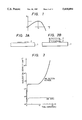
FIG. 13 is a graph showing an example of the relationship between the flow rate ratio of SiH4 and NH3 and the composition ratio of Si and N in the silicon nitride film formed.
The deposition conditions at this time were an RF output of 175 W, a substrate temperature of 380° C. and the flow rate of NH3 gas was varied with the SiH4 gas flow rate being fixed at cc/min. As shown in the graph, by varying the gas flow rate ratio of NH3 /SiH4 from 4 to 10, the Si/N ratio in the silicon nitride film was found to be varied from 1.1 to 0.58 according to Auger's electron spectrophotometry.
On the other hand, the composition of the silicon nitride film formed according to the reduced pressure CVD method by introducing SiH2 Cl2 gas and NH3 gas under the conditions of a reduced pressure of 0.3 Torr and a temperature of about 800° C., was found to be Si3 N4 (Si/N=0.75) which is approximately the stoichiometric ratio.
Also, the silicon nitride film formed by heat treatment at about 1200° C. in ammonia or N2 (hot nitrification method) can be obtained with a composition further approximate to the stoichiometric ratio, since the formation method is performed under thermal equilibrium.
By use of silicon nitrides formed by the various methods as described above as the material for forming nucleation surface (SNDL) with higher nucleation density than SiO2, the above nucleus of Si can be grown on the nucleation surface (SNDL) comprising silicon nitride to form a Si single crystal based on the nucleation density (ΔND) corresponding to the chemical composition ratio of silicon nitride.
FIG. 14 is a graph showing the relationship between Si/N composition ratio and nucleation density (ΔND). As shown in the same graph, by varying the chemical composition ratio of the silicon nitride film, the nucleation density of the Si single crystal nucleus formed thereon changes to a great extent. The nucleation conditions in the graph shown in FIG. 17 correspond to the case when a Si single crystal nucleus was formed by reacting SiCl4 gas reduced to 175 Torr with H2 at 1000° C. Of course, another graph will be obtained if nucleation conditions such as gas species, pressure, temperature, etc., are changed.
The phenomenon that the nucleation density thus changes according to the chemical composition ratio of silicon nitride affects the size (area) of the nucleation surface (SNDL) when employing silicon nitride as the material for forming the nucleation surface (SNDL) which is formed to be sufficiently small to the extent that a single nucleus may be grown. That is, when employing silicon nitride having a composition with great nucleation density (ND) only a single crystal can be formed on the nucleation surface (SNDL) by forming the nucleation surface (SNDL) extremely small as compared with the silicon nitride with a relatively smaller nucleation density (ND). Such a point is applicable as a similar tendency for other materials for forming a nucleation surface (SNDL). Accordingly, in the present invention, for accomplishing its objects effectively, it is desirable to select a nucleation density (ND) and a size of the nucleation surface (SNDL) formed of silicon nitride, etc., capable of forming only a single crystal suitably as desired. For example, under the nucleation condition for obtaining a nucleation density (ND) of about 105 cm-2 or less, it is possible to form selectively, only a single nucleus,.if the size of the nucleation surface (SNDL) comprising silicon nitride is about 4 μm or less. The Si/N ratio in that case is about 0.5.
Formation of Nucleation Surface (SNDL) by Ion Injection
As another method for realizing nucleation density difference when forming a Si single crystal nucleus by ion injection of Si, N, P, B, F, Ar, He, C, As, Ga, Ge, etc., may be effected locally onto the surface comprising SiO2 which is a material for forming nonnucleation surface (SNDS) with smaller nucleation density to form a modified region with a desired size on the SiO2 surface, and utilize this modified region as the nucleation surface (SNDL) with greater nucleation density (ND).
For example, the SiO2 layer surface is covered with a photoresist layer and the desired portions are exposed, developed and dissolved to have the SiO2 layer surface exposed.
Subsequently, by use of SiF4 gas as the source gas, Si ions are implanted onto the SiO2 layer surface exposed at 10 keV at a density of 1×10¹⁶ ˜1×1018 cm-2. The projected flying distance in this case is 114 Å, and the Si concentration on the exposed surface of SiO2 layer reaches about 1022 cm-3 or less. Since the SiO2 layer is originally amorphous, the modified layer made excessively enriched in Si by injection of Si ions is also amorphous.
For formation of a modified region, ion injection can be effected with the use of a resist as the mask, but it is also possible to inject a narrowed Si ion beam selectively at a desired position on the SiO2 layer surface within a desired area without use of a resist mark by use of a converged ion beam technique.
After having thus effected Si ion injection, by peeling of the resist on the remaining portion, a Si-excessive modified region is formed on the SiO2 layer surface at a desired position with a desired size. On the modified region of the SiO2 layer surface on which such a modified region is formed, a Si single crystal is permitted to grow in the vapor phase.
FIG. 15 is a graph showing the relationship between the amount of Si ions injected and the nucleation density (ND).
As shown in the graph, it can be understood that the nucleation density (ND) is increased as the amount of Si+ injected is increased.
Accordingly, by forming a sufficiently small modified region, only a single nucleus of Si can be grown with the modified region being the nucleation surface (SNDL), whereby a single crystal can be grown as described above.
This can be easily accomplished by patterning of a resist or narrowing of the beam of the converged ion beam to form a sufficiently small modified region to the extent that only a single nucleus may grow.
Method for Formation of Si Single Crystal Nucleus Other Than CVD
For growth of a single crystal by selective nucleation of Si, not only the CVD method, but also the method by evaporation of Si into a vacuum (<10-6 Torr ) with an electron gun and deposition on a heated substrate may be used. Particularly, in the MBE (Molecular Beam Epitaxy) method which performs vapor deposition in an ultra-high vacuum (<10-9 Torr), it has been known that an Si beam begins to react with SiO2 at a substrate temperature of 900° C. or higher, whereby no nucleation of Si occurs on SiO2 at all (T. Yonehara, S. Yoshioka and S. Miyazawa, Journal of Applied Physics 53, 10, p. 6839, 1983).
By utilizing this phenomenon, a single crystal nuclei of Si can be formed with perfect selectivity on the small silicon nitride regions permitted to exist in spots on the SiO2 layer, and a single crystal Si can be grown thereon. The single crystal growth conditions as preferable example at this time may be, for example, a vacuum degree of 10-8 Torr or lower, a Si beam intensity of 9.7×10¹⁴ atoms/cm2 ·sec, and a substrate temperature of 900° C.˜1000° C.
In this case, through the reaction SiO2 +Si→2SiO↑, a reaction product of SiO with a remarkably high vapor pressure is formed, and etching of SiO2 itself with Si through this evaporation occurs.
In contrast, no such etching phenomenon as mentioned above occurs on silicon nitride, but nucleation of a Si single crystal and growth of a single crystal occur.
Accordingly, as the material for forming the nucleation surface (SNDL) with high nucleation density (ND), tantalum oxide (Ta2 O5), silicon nitride oxide (SION), etc., can be also used other than silicon nitride to obtain the same effect. That is, by forming the above nucleation surface (SNDL) with these materials in small areas, single crystals of Si can be permitted to grow similarly.
FIG. 16 is a sectional view showing an embodiment of the photoelectric conversion device according to the present invention. In the Figure, there are laid on a p-type silicon substrate 101, a first layer formed with a bipolar transistor 102, a second layer formed with a MOS transistor 103 and a third layer (top layer) formed with a photodiode 104.
The bipolar transistor 102 of the first layer is formed in the substrate 101 using a conventional integrated circuit manufacturing process. First, a buried layer 105 is formed in the p-type substrate 101 by diffusing an impurity such as As, Sb or P. There is formed on the buried layer 105 an n-epitaxial layer 106 serving as a collector region.
A p-base region 107 is formed in the n-epitaxial layer 106 by diffusing an impurity such as boron. An n+ -emitter region 108 is formed in the p-base region by diffusing an impurity such as P or As. After forming a p-type element isolation region 109 by impurity diffusion, the whole surface is covered with an insulation layer 110. Contact holes are made to form an emitter electrode and a base electrode, and a collector electrode via an ohmic contact layer.
In this embodiment, then an interlayer insulation layer 111 is formed using SiO2 which is not only a deposition surface forming material with a small nucleation density but also an insulation material. The interlayer insulation layer 111 is formed by the CVD method. It is preferable to further make the surface even by the known process.
Next, there is formed on the interlayer insulation layer 111 a nucleus forming region 113 of minute area, using a material having a sufficient nucleation density higher than that of SiO2. In this embodiment, silicon nitride is used as such a material to form a p-type silicon monocrystalline layer 114 of 1.2 micron square to be later described, under a temperature of 700° to 1000° C. which does not deteriorate the characteristics of the bipolar transistor in the first layer.
Next, a gate insulation layer 115A on the p-type monocrystalline silicon layer 114 is formed to pattern the gate electrode 115. Thereafter, a source/drain region is formed through n-type impurity diffusion and other necessary interconnections are formed, to thereby complete the second layer having the n-channel MOS transistor.
Contact holes are opened in the interlayer insulation layer 111 to connect the MOS transistor 103 to the bipolar transistor 102 and the like via interconnections 112.
Next, an interlayer insulation layer 116 is formed on the second layer. An n-type monocrystalline silicon layer 119 is formed by the selective nucleus forming crystal grow method, using a nucleus forming region of a small area made of the above-described material. Succeedingly, a P-type region 120 is formed in the monocrystalline silicon layer 119 through p-type impurity diffusion, to thereby form the photodiode 104 with a pn junction. Contact holes are opened in the interlayer insulation layer 116 to connect the photodiode 104 to the MOS transistor in the lower layer via interconnections 117.
By forming a plurality of photodiodes 104 in the top layer, a photoelectric conversion device of good sensitivity can be realized because incident light can be applied efficiently to the photodiodes 104.
Further, since the monocrystalline silicon layer can be formed at a low temperature of the order of 700° to 1000° C., elements in the lower layer are not deteriorated in their characteristics. The mobility in channel of the MOS transistor 103 is larger than 400 cm2 /V sec, which is more than ten times of that of a conventional MOS transistor formed in a polysilicon layer.
FIG. 17 is an example of a fundamental circuit of the embodiment shown in FIG. 16. In the Figure, photodiodes 104 are arranged in an array, one end of which are applied with a source voltage and the other end are coupled via MOS transistors 103 to an amplifier 102 made of bipolar transistors. Outputs of the photodiodes are scanned in response to control signals applied to the gate electrodes 115 of the MOS transistors 103, and are serially sent to the amplifier 102.
In the above embodiment, since outputs from the photodiodes are processed by the high performance MOS transistors 103 and bipolar transistors in the monocrystalline layer, a high speed operation is possible.
Although a monocrystalline layer has been formed on the interlayer insulation layer in the above embodiment, a polysilicon layer may be formed as necessary. The process for forming a polysilicon layer has been described previously.
A three-layered structure has been employed in the above embodiment. It is obvious that the circuit section may be formed in a multi-layered structure having optional layers. For instance, a signal read section, a calculation section, a memory section and the like may be formed separately in a different layer.
Further, a photodiode has been used as a photosensor. Obviously, another type of photosensor such as a phototransistor may be used.
As described so far, the photoelectric conversion device of this embodiment improves the aperture ratio of the device and attains a high sensitivity. Further, by using the above-described method of forming a crystal layer, a monocrystal can be grown easily even on a substrate made of amorphous material. Thus, a high performance photosensor, field effect transistor, bipolar transistor and the like can be formed as a multi-layered integrated circuit structure. As a result, a photoelectric conversion device can be realized which operates at high speed and has various functions.

Claims (14)

We claim:
1. A method for fabricating a photoelectric conversion device, said method comprising the steps of:
forming a substrate having a first semiconductor element of the photoelectric conversion device therein;
forming, on the substrate, an insulating layer of a first material;
forming, by deposition on a surface of the insulating layer, a seed of amorphous material different from the first material;
selecting a vapor deposition growth process in which the first material of the insulating layer has a nucleation density sufficiently smaller than a nucleation density of the amorphous material that substantially all crystal growth occurs on the amorphous material and substantially no crystal growth occurs on the insulating layer, the seed of amorphous material having an area sized so as to form only one nucleus during crystal growth in the selected vapor deposition crystal growth process;
applying the selected vapor deposition crystal growth process to grow the nucleus from the seed;
continuing the selected vapor deposition crystal growth process to grow, from the nucleus, a thin film single crystal layer over at least a portion of the surface of the insulating layer; and
forming a photoelectric conversion device using the single crystal layer and including the first semiconductor element.
2. A method according to claim 1, wherein the vapor deposition is a chemical vapor deposition process.
3. A method according to claim 1, wherein the insulating layer is composed of SiO2.
4. A method according to claim 1, wherein the seed is composed of Si3 N4.
5. A method according to claim 1, wherein the semiconductor substrate comprises a silicon semiconductor.
6. A method according to claim 1, wherein said first semiconductor element comprises a signal amplifying element.
7. A method for fabricating a photoelectric conversion device, said method comprising the steps of:
forming a substrate having a first semiconductor element of the photoelectric conversion device therein;
forming, on the substrate, an insulating layer of a first material;
forming, on a surface of the insulating layer, a seed of amorphous material comprising a region of modified composition formed in an ion implantation process;
selecting a vapor deposition growth process in which the first material of the insulating layer has a nucleation density sufficiently smaller than a nucleation density of the amorphous material that substantially all crystal growth occurs on the amorphous material and substantially no crystal growth occurs on the insulating layer, the seed of amorphous material having an area sized so as to form only one nucleus during crystal growth in the selected vapor deposition crystal growth process;
applying the selected vapor deposition crystal growth process to grow the nucleus from the seed;
continuing the selected vapor deposition crystal growth process to grow, from the nucleus, a thin film single crystal layer over at least a portion of the surface of the insulating layer; and
forming a photoelectric conversion device using the single crystal layer and including the first semiconductor element.
8. A method according to claim 7, wherein the vapor deposition is a chemical vapor deposition process.
9. A method according to claim 7, wherein the insulating layer is composed of SiO2.
10. A method according to claim 7, wherein the seed is composed of Si3 N4.
11. A method according to claim 7, wherein the semiconductor substrate comprises a silicon semiconductor.
12. A method according to claim 7, wherein said first semiconductor element comprises a signal amplifying element.
13. A method according to claim 1, wherein the nucleation density of the amorphous material is at least about 103 times the nucleation density of the first material.
14. A method according to claim 7, wherein the nucleation density of the amorphous material is at least about 103 times the nucleation density of the first material.
US08/475,830 1986-07-11 1995-06-07 Photoelectric conversion device Expired - Fee Related US5610094A (en)

Priority Applications (1)

Application Number Priority Date Filing Date Title
US08/475,830 US5610094A (en) 1986-07-11 1995-06-07 Photoelectric conversion device

Applications Claiming Priority (9)

Application Number Priority Date Filing Date Title
JP61162129A JP2505754B2 (en) 1986-07-11 1986-07-11 Method for manufacturing photoelectric conversion device
JP61-162129 1986-07-11
US7077887A 1987-07-07 1987-07-07
US36183089A 1989-06-05 1989-06-05
US81584691A 1991-12-31 1991-12-31
US97023492A 1992-11-02 1992-11-02
US9343793A 1993-07-08 1993-07-08
US27030494A 1994-07-05 1994-07-05
US08/475,830 US5610094A (en) 1986-07-11 1995-06-07 Photoelectric conversion device

Related Parent Applications (1)

Application Number Title Priority Date Filing Date
US27030494A Continuation 1986-07-11 1994-07-05

Publications (1)

Publication Number Publication Date
US5610094A true US5610094A (en) 1997-03-11

Family

ID=15748590

Family Applications (1)

Application Number Title Priority Date Filing Date
US08/475,830 Expired - Fee Related US5610094A (en) 1986-07-11 1995-06-07 Photoelectric conversion device

Country Status (7)

Country Link
US (1) US5610094A (en)
EP (1) EP0252757B1 (en)
JP (1) JP2505754B2 (en)
AT (1) ATE159125T1 (en)
AU (1) AU609405B2 (en)
CA (1) CA1301896C (en)
DE (1) DE3752126T2 (en)

Cited By (12)

* Cited by examiner, † Cited by third party
Publication number Priority date Publication date Assignee Title
US5770482A (en) * 1996-10-08 1998-06-23 Advanced Micro Devices, Inc. Multi-level transistor fabrication method with a patterned upper transistor substrate and interconnection thereto
US5770483A (en) * 1996-10-08 1998-06-23 Advanced Micro Devices, Inc. Multi-level transistor fabrication method with high performance drain-to-gate connection
US5814542A (en) * 1996-01-09 1998-09-29 Nec Corporation Fabrication method of semiconductor device with MOSFET and capacitor having lower and upper polysilicon regions
US6037602A (en) * 1998-02-13 2000-03-14 C.P. Clare Corporation Photovoltaic generator circuit and method of making same
US6075268A (en) * 1996-11-07 2000-06-13 Advanced Micro Devices, Inc. Ultra high density inverter using a stacked transistor arrangement
US6077781A (en) * 1995-11-21 2000-06-20 Applied Materials, Inc. Single step process for blanket-selective CVD aluminum deposition
US6172381B1 (en) 1997-06-20 2001-01-09 Advanced Micro Devices, Inc. Source/drain junction areas self aligned between a sidewall spacer and an etched lateral sidewall
US6232637B1 (en) 1997-05-02 2001-05-15 Advanced Micro Devices, Inc. Semiconductor fabrication having multi-level transistors and high density interconnect therebetween
US6358828B1 (en) 1997-06-20 2002-03-19 Advanced Micro Devices, Inc. Ultra high density series-connected transistors formed on separate elevational levels
US20030003766A1 (en) * 2001-05-31 2003-01-02 Hideya Kumomi Crystalline thin film and process for production thereof, element employing crystalline thin film, circuit employing element, and device employing element or circuit
US20050121707A1 (en) * 2003-05-30 2005-06-09 Canon Kabushiki Kaisha Solid-state image sensing apparatus and method of manufacturing the same
US20140225214A1 (en) * 2002-12-18 2014-08-14 Infrared Newco, Inc. Image sensor comprising isolated germanium photodetectors integrated with a silicon substrate and silicon circuitry

Families Citing this family (3)

* Cited by examiner, † Cited by third party
Publication number Priority date Publication date Assignee Title
JP2516604B2 (en) * 1986-10-17 1996-07-24 キヤノン株式会社 Method for manufacturing complementary MOS integrated circuit device
JP4820713B2 (en) * 2006-08-10 2011-11-24 住友重機械工業株式会社 Decelerator
JP6570417B2 (en) * 2014-10-24 2019-09-04 株式会社半導体エネルギー研究所 Imaging apparatus and electronic apparatus

Citations (20)

* Cited by examiner, † Cited by third party
Publication number Priority date Publication date Assignee Title
US3620833A (en) * 1966-12-23 1971-11-16 Texas Instruments Inc Integrated circuit fabrication
EP0020135A1 (en) * 1979-05-29 1980-12-10 Massachusetts Institute Of Technology Three-dimensional integration by graphoepitaxy
JPS57106181A (en) * 1980-12-24 1982-07-01 Toshiba Corp Integrated circuit
US4340819A (en) * 1978-12-22 1982-07-20 Nippon Kogaku K.K. Photoelectric element array with automatic control of the charge storage time
JPS5892254A (en) * 1981-11-27 1983-06-01 Mitsubishi Electric Corp Semiconductor device
GB2113465A (en) * 1982-01-12 1983-08-03 Rca Corp Method for growing monocrystalline silicon on a masking layer
GB2116067A (en) * 1982-02-26 1983-09-21 Rca Corp Method for growing a low defect monocrystalline layer on a mask
US4471371A (en) * 1981-01-06 1984-09-11 Fuji Xerox Co., Ltd. Thin film image pickup element
US4472729A (en) * 1981-08-31 1984-09-18 Tokyo Shibaura Denki Kabushiki Kaisha Recrystallized three dimensional integrated circuit
US4651016A (en) * 1983-07-28 1987-03-17 Mitsubishi Denki Kabushiki Kaisha Solid-state image sensor provided with a bipolar transistor and an MOS transistor
GB2183090A (en) * 1985-10-07 1987-05-28 Canon Kk Method for selective formation of deposited film
US4686554A (en) * 1983-07-02 1987-08-11 Canon Kabushiki Kaisha Photoelectric converter
US4686758A (en) * 1984-06-27 1987-08-18 Honeywell Inc. Three-dimensional CMOS using selective epitaxial growth
US4751561A (en) * 1986-04-29 1988-06-14 Rca Corporation Dielectrically isolated PMOS, NMOS, PNP and NPN transistors on a silicon wafer
US4977096A (en) * 1987-06-30 1990-12-11 Canon Kabushiki Kaisha Method of making a photosensor using selective epitaxial growth
US4983539A (en) * 1987-02-28 1991-01-08 Canon Kabushiki Kaisha Process for producing a semiconductor article
US4999313A (en) * 1986-11-07 1991-03-12 Canon Kabushiki Kaisha Preparation of a semiconductor article using an amorphous seed to grow single crystal semiconductor material
US5008206A (en) * 1986-07-11 1991-04-16 Canon Kabushiki Kaisha Method for making a photoelectric conversion device using an amorphous nucleation site
US5010033A (en) * 1987-03-27 1991-04-23 Canon Kabushiki Kaisha Process for producing compound semiconductor using an amorphous nucleation site
US5013670A (en) * 1986-09-18 1991-05-07 Canon Kabushiki Kaisha Photoelectric converter

Family Cites Families (5)

* Cited by examiner, † Cited by third party
Publication number Priority date Publication date Assignee Title
JPS5856323A (en) * 1981-09-29 1983-04-04 Nec Corp Manufacture of semiconductor substrate
JPS587819A (en) * 1981-07-07 1983-01-17 Nec Corp Vapor growth method
JPS5918196A (en) * 1982-07-21 1984-01-30 Hitachi Ltd Preparation of thin film of single crystal
JPS60178662A (en) * 1984-02-24 1985-09-12 Toshiba Corp Semiconductor device
JPH0782996B2 (en) * 1986-03-28 1995-09-06 キヤノン株式会社 Crystal formation method

Patent Citations (20)

* Cited by examiner, † Cited by third party
Publication number Priority date Publication date Assignee Title
US3620833A (en) * 1966-12-23 1971-11-16 Texas Instruments Inc Integrated circuit fabrication
US4340819A (en) * 1978-12-22 1982-07-20 Nippon Kogaku K.K. Photoelectric element array with automatic control of the charge storage time
EP0020135A1 (en) * 1979-05-29 1980-12-10 Massachusetts Institute Of Technology Three-dimensional integration by graphoepitaxy
JPS57106181A (en) * 1980-12-24 1982-07-01 Toshiba Corp Integrated circuit
US4471371A (en) * 1981-01-06 1984-09-11 Fuji Xerox Co., Ltd. Thin film image pickup element
US4472729A (en) * 1981-08-31 1984-09-18 Tokyo Shibaura Denki Kabushiki Kaisha Recrystallized three dimensional integrated circuit
JPS5892254A (en) * 1981-11-27 1983-06-01 Mitsubishi Electric Corp Semiconductor device
GB2113465A (en) * 1982-01-12 1983-08-03 Rca Corp Method for growing monocrystalline silicon on a masking layer
GB2116067A (en) * 1982-02-26 1983-09-21 Rca Corp Method for growing a low defect monocrystalline layer on a mask
US4686554A (en) * 1983-07-02 1987-08-11 Canon Kabushiki Kaisha Photoelectric converter
US4651016A (en) * 1983-07-28 1987-03-17 Mitsubishi Denki Kabushiki Kaisha Solid-state image sensor provided with a bipolar transistor and an MOS transistor
US4686758A (en) * 1984-06-27 1987-08-18 Honeywell Inc. Three-dimensional CMOS using selective epitaxial growth
GB2183090A (en) * 1985-10-07 1987-05-28 Canon Kk Method for selective formation of deposited film
US4751561A (en) * 1986-04-29 1988-06-14 Rca Corporation Dielectrically isolated PMOS, NMOS, PNP and NPN transistors on a silicon wafer
US5008206A (en) * 1986-07-11 1991-04-16 Canon Kabushiki Kaisha Method for making a photoelectric conversion device using an amorphous nucleation site
US5013670A (en) * 1986-09-18 1991-05-07 Canon Kabushiki Kaisha Photoelectric converter
US4999313A (en) * 1986-11-07 1991-03-12 Canon Kabushiki Kaisha Preparation of a semiconductor article using an amorphous seed to grow single crystal semiconductor material
US4983539A (en) * 1987-02-28 1991-01-08 Canon Kabushiki Kaisha Process for producing a semiconductor article
US5010033A (en) * 1987-03-27 1991-04-23 Canon Kabushiki Kaisha Process for producing compound semiconductor using an amorphous nucleation site
US4977096A (en) * 1987-06-30 1990-12-11 Canon Kabushiki Kaisha Method of making a photosensor using selective epitaxial growth

Non-Patent Citations (10)

* Cited by examiner, † Cited by third party
Title
"Single-crystal films of silicon on insulators" by J. D. Filby et al., Brit. J. Appl. Phys., 1967, vol. 18, pp. 1357-1382.
S. Kataoka, "An Attempt Towards an Artificial Retina: 3-D IC Technology For An Intelligent Image Sensor", Transducers '85, 1985 Int'l Conf. on Solid State Sensors and Actuators Digest of of Technical Papers, IEEE, pp. 440-442.
S. Kataoka, An Attempt Towards an Artificial Retina: 3 D IC Technology For An Intelligent Image Sensor , Transducers 85, 1985 Int l Conf. on Solid State Sensors and Actuators Digest of of Technical Papers, IEEE, pp. 440 442. *
Single crystal films of silicon on insulators by J. D. Filby et al., Brit. J. Appl. Phys., 1967, vol. 18, pp. 1357 1382. *
T. Yonehara, et al., "Competing Processes of Si Molecular Beam Reactive Etching and Simultaneous Deposition On Film and Bulk SiO2 ", Journal of Applied Physics, vol. 53, No. 10, pp. 6839-6843 (Oct. 1982).
T. Yonehara, et al., Competing Processes of Si Molecular Beam Reactive Etching and Simultaneous Deposition On Film and Bulk SiO 2 , Journal of Applied Physics, vol. 53, No. 10, pp. 6839 6843 (Oct. 1982). *
W. A. P. Clausen, "The Nucleation of CVD Silicon on SiO2 and Si3N4 Substrates", Journal of the Electrochemical Society, vol. 128, No. 6, Jun. 1981, pp. 1353-1359.
W. A. P. Clausen, The Nucleation of CVD Silicon on SiO 2 and Si3N4 Substrates , Journal of the Electrochemical Society, vol. 128, No. 6, Jun. 1981, pp. 1353 1359. *
Wolf, S., Tauber, R.; Silicon Processing for the VLSI Era vol. I: Process Technology (1986) pp. 280 283 & 288 292. *
Wolf, S., Tauber, R.; Silicon Processing for the VLSI Era vol. I: Process Technology (1986) pp. 280-283 & 288-292.

Cited By (18)

* Cited by examiner, † Cited by third party
Publication number Priority date Publication date Assignee Title
US6458684B1 (en) 1995-11-21 2002-10-01 Applied Materials, Inc. Single step process for blanket-selective CVD aluminum deposition
US6077781A (en) * 1995-11-21 2000-06-20 Applied Materials, Inc. Single step process for blanket-selective CVD aluminum deposition
US5814542A (en) * 1996-01-09 1998-09-29 Nec Corporation Fabrication method of semiconductor device with MOSFET and capacitor having lower and upper polysilicon regions
US5770483A (en) * 1996-10-08 1998-06-23 Advanced Micro Devices, Inc. Multi-level transistor fabrication method with high performance drain-to-gate connection
US5852310A (en) * 1996-10-08 1998-12-22 Advanced Micro Devices, Inc. Multi-level transistor fabrication method with a patterned upper transistor substrate and interconnection thereto
US5770482A (en) * 1996-10-08 1998-06-23 Advanced Micro Devices, Inc. Multi-level transistor fabrication method with a patterned upper transistor substrate and interconnection thereto
US6075268A (en) * 1996-11-07 2000-06-13 Advanced Micro Devices, Inc. Ultra high density inverter using a stacked transistor arrangement
US6232637B1 (en) 1997-05-02 2001-05-15 Advanced Micro Devices, Inc. Semiconductor fabrication having multi-level transistors and high density interconnect therebetween
US6172381B1 (en) 1997-06-20 2001-01-09 Advanced Micro Devices, Inc. Source/drain junction areas self aligned between a sidewall spacer and an etched lateral sidewall
US6358828B1 (en) 1997-06-20 2002-03-19 Advanced Micro Devices, Inc. Ultra high density series-connected transistors formed on separate elevational levels
US6037602A (en) * 1998-02-13 2000-03-14 C.P. Clare Corporation Photovoltaic generator circuit and method of making same
US20030003766A1 (en) * 2001-05-31 2003-01-02 Hideya Kumomi Crystalline thin film and process for production thereof, element employing crystalline thin film, circuit employing element, and device employing element or circuit
US7115487B2 (en) 2001-05-31 2006-10-03 Canon Kabushiki Kaisha Crystalline thin film and process for production thereof, element employing crystalline thin film, circuit employing element, and device employing element or circuit
US20140225214A1 (en) * 2002-12-18 2014-08-14 Infrared Newco, Inc. Image sensor comprising isolated germanium photodetectors integrated with a silicon substrate and silicon circuitry
US9142585B2 (en) * 2002-12-18 2015-09-22 Infrared Newco, Inc. Image sensor comprising isolated germanium photodetectors integrated with a silicon substrate and silicon circuitry
US20050121707A1 (en) * 2003-05-30 2005-06-09 Canon Kabushiki Kaisha Solid-state image sensing apparatus and method of manufacturing the same
US20060199296A1 (en) * 2003-05-30 2006-09-07 Canon Kabushiki Kaisha Solid-state image sensing apparatus and method of manufacturing the same
US7732238B2 (en) 2003-05-30 2010-06-08 Canon Kabushiki Kaisha Method of manufacturing an image sensing apparatus in which two members are bonded together

Also Published As

Publication number Publication date
AU7539187A (en) 1988-01-14
AU609405B2 (en) 1991-05-02
CA1301896C (en) 1992-05-26
EP0252757A2 (en) 1988-01-13
JP2505754B2 (en) 1996-06-12
EP0252757B1 (en) 1997-10-08
EP0252757A3 (en) 1988-08-31
DE3752126D1 (en) 1997-11-13
DE3752126T2 (en) 1998-03-12
ATE159125T1 (en) 1997-10-15
JPS6318668A (en) 1988-01-26

Similar Documents

Publication Publication Date Title
US5236546A (en) Process for producing crystal article
US5008206A (en) Method for making a photoelectric conversion device using an amorphous nucleation site
US5028976A (en) Complementary MOS integrated circuit device
US5269876A (en) Process for producing crystal article
US5422302A (en) Method for producing a three-dimensional semiconductor device
US5733369A (en) Method for forming crystal
US5610094A (en) Photoelectric conversion device
US4999313A (en) Preparation of a semiconductor article using an amorphous seed to grow single crystal semiconductor material
US5846320A (en) Method for forming crystal and crystal article obtained by said method
US5087296A (en) Solar battery and process for preparing same
US5086326A (en) Photoelectric conversion device
CA1296816C (en) Process for producing a semiconductor article
AU651805B2 (en) Method for forming crystal and crystal article obtained by said method
JP2695413B2 (en) Manufacturing method of crystal substrate
EP0276959B1 (en) Process for producing crystal article
US5364815A (en) Crystal articles and method for forming the same
EP0284433B1 (en) Crystal articles and method for forming the same
JP2651145B2 (en) Manufacturing method of semiconductor substrate
US5463975A (en) Process for producing crystal
JP2515301B2 (en) Method for manufacturing semiconductor device
JP2525773B2 (en) Semiconductor device and manufacturing method thereof
JPH04373121A (en) Manufacture of crystal base material
JPS63239979A (en) Photosensor and manufacture thereof
JPS63239978A (en) Optical sensor for image input

Legal Events

Date Code Title Description
CC Certificate of correction
FEPP Fee payment procedure

Free format text: PAYOR NUMBER ASSIGNED (ORIGINAL EVENT CODE: ASPN); ENTITY STATUS OF PATENT OWNER: LARGE ENTITY

Free format text: PAYER NUMBER DE-ASSIGNED (ORIGINAL EVENT CODE: RMPN); ENTITY STATUS OF PATENT OWNER: LARGE ENTITY

FPAY Fee payment

Year of fee payment: 4

REMI Maintenance fee reminder mailed
LAPS Lapse for failure to pay maintenance fees

Free format text: PATENT EXPIRED FOR FAILURE TO PAY MAINTENANCE FEES (ORIGINAL EVENT CODE: EXP.); ENTITY STATUS OF PATENT OWNER: LARGE ENTITY

STCH Information on status: patent discontinuation

Free format text: PATENT EXPIRED DUE TO NONPAYMENT OF MAINTENANCE FEES UNDER 37 CFR 1.362

FP Lapsed due to failure to pay maintenance fee

Effective date: 20050311