US5523246A - Method of fabricating a high-voltage metal-gate CMOS device - Google Patents
Method of fabricating a high-voltage metal-gate CMOS device Download PDFInfo
- Publication number
- US5523246A US5523246A US08/490,221 US49022195A US5523246A US 5523246 A US5523246 A US 5523246A US 49022195 A US49022195 A US 49022195A US 5523246 A US5523246 A US 5523246A
- Authority
- US
- United States
- Prior art keywords
- conductivity type
- drain regions
- openings
- doped source
- impurities
- Prior art date
- Legal status (The legal status is an assumption and is not a legal conclusion. Google has not performed a legal analysis and makes no representation as to the accuracy of the status listed.)
- Expired - Lifetime
Links
- 238000004519 manufacturing process Methods 0.000 title claims abstract description 18
- 239000000758 substrate Substances 0.000 claims abstract description 28
- 239000012535 impurity Substances 0.000 claims abstract description 21
- 239000004065 semiconductor Substances 0.000 claims abstract description 18
- 229910052751 metal Inorganic materials 0.000 claims abstract description 14
- 239000002184 metal Substances 0.000 claims abstract description 14
- 230000004888 barrier function Effects 0.000 claims abstract description 13
- 125000006850 spacer group Chemical group 0.000 claims abstract description 12
- 238000007669 thermal treatment Methods 0.000 claims abstract description 11
- 238000000034 method Methods 0.000 claims description 23
- 238000005530 etching Methods 0.000 claims description 7
- 238000000059 patterning Methods 0.000 claims description 2
- VYPSYNLAJGMNEJ-UHFFFAOYSA-N Silicium dioxide Chemical group O=[Si]=O VYPSYNLAJGMNEJ-UHFFFAOYSA-N 0.000 claims 2
- 229910052581 Si3N4 Inorganic materials 0.000 claims 1
- 235000012239 silicon dioxide Nutrition 0.000 claims 1
- 239000000377 silicon dioxide Substances 0.000 claims 1
- HQVNEWCFYHHQES-UHFFFAOYSA-N silicon nitride Chemical group N12[Si]34N5[Si]62N3[Si]51N64 HQVNEWCFYHHQES-UHFFFAOYSA-N 0.000 claims 1
- 229910021420 polycrystalline silicon Inorganic materials 0.000 description 4
- 229920005591 polysilicon Polymers 0.000 description 4
- -1 boron ions Chemical class 0.000 description 3
- 238000005229 chemical vapour deposition Methods 0.000 description 3
- 238000001459 lithography Methods 0.000 description 3
- 229910052796 boron Inorganic materials 0.000 description 2
- 238000002513 implantation Methods 0.000 description 2
- 230000003647 oxidation Effects 0.000 description 2
- 238000007254 oxidation reaction Methods 0.000 description 2
- 238000001020 plasma etching Methods 0.000 description 2
- 229910052782 aluminium Inorganic materials 0.000 description 1
- XAGFODPZIPBFFR-UHFFFAOYSA-N aluminium Chemical compound [Al] XAGFODPZIPBFFR-UHFFFAOYSA-N 0.000 description 1
- 229910052785 arsenic Inorganic materials 0.000 description 1
- 230000000295 complement effect Effects 0.000 description 1
- 150000002500 ions Chemical class 0.000 description 1
Images


Classifications
-
- H—ELECTRICITY
- H01—ELECTRIC ELEMENTS
- H01L—SEMICONDUCTOR DEVICES NOT COVERED BY CLASS H10
- H01L29/00—Semiconductor devices adapted for rectifying, amplifying, oscillating or switching, or capacitors or resistors with at least one potential-jump barrier or surface barrier, e.g. PN junction depletion layer or carrier concentration layer; Details of semiconductor bodies or of electrodes thereof ; Multistep manufacturing processes therefor
- H01L29/66—Types of semiconductor device ; Multistep manufacturing processes therefor
- H01L29/66007—Multistep manufacturing processes
- H01L29/66075—Multistep manufacturing processes of devices having semiconductor bodies comprising group 14 or group 13/15 materials
- H01L29/66227—Multistep manufacturing processes of devices having semiconductor bodies comprising group 14 or group 13/15 materials the devices being controllable only by the electric current supplied or the electric potential applied, to an electrode which does not carry the current to be rectified, amplified or switched, e.g. three-terminal devices
- H01L29/66409—Unipolar field-effect transistors
- H01L29/66477—Unipolar field-effect transistors with an insulated gate, i.e. MISFET
- H01L29/66568—Lateral single gate silicon transistors
-
- H—ELECTRICITY
- H01—ELECTRIC ELEMENTS
- H01L—SEMICONDUCTOR DEVICES NOT COVERED BY CLASS H10
- H01L21/00—Processes or apparatus adapted for the manufacture or treatment of semiconductor or solid state devices or of parts thereof
- H01L21/70—Manufacture or treatment of devices consisting of a plurality of solid state components formed in or on a common substrate or of parts thereof; Manufacture of integrated circuit devices or of parts thereof
- H01L21/77—Manufacture or treatment of devices consisting of a plurality of solid state components or integrated circuits formed in, or on, a common substrate
- H01L21/78—Manufacture or treatment of devices consisting of a plurality of solid state components or integrated circuits formed in, or on, a common substrate with subsequent division of the substrate into plural individual devices
- H01L21/82—Manufacture or treatment of devices consisting of a plurality of solid state components or integrated circuits formed in, or on, a common substrate with subsequent division of the substrate into plural individual devices to produce devices, e.g. integrated circuits, each consisting of a plurality of components
- H01L21/822—Manufacture or treatment of devices consisting of a plurality of solid state components or integrated circuits formed in, or on, a common substrate with subsequent division of the substrate into plural individual devices to produce devices, e.g. integrated circuits, each consisting of a plurality of components the substrate being a semiconductor, using silicon technology
- H01L21/8232—Field-effect technology
- H01L21/8234—MIS technology, i.e. integration processes of field effect transistors of the conductor-insulator-semiconductor type
- H01L21/8238—Complementary field-effect transistors, e.g. CMOS
- H01L21/823814—Complementary field-effect transistors, e.g. CMOS with a particular manufacturing method of the source or drain structures, e.g. specific source or drain implants or silicided source or drain structures or raised source or drain structures
-
- H—ELECTRICITY
- H01—ELECTRIC ELEMENTS
- H01L—SEMICONDUCTOR DEVICES NOT COVERED BY CLASS H10
- H01L29/00—Semiconductor devices adapted for rectifying, amplifying, oscillating or switching, or capacitors or resistors with at least one potential-jump barrier or surface barrier, e.g. PN junction depletion layer or carrier concentration layer; Details of semiconductor bodies or of electrodes thereof ; Multistep manufacturing processes therefor
- H01L29/66—Types of semiconductor device ; Multistep manufacturing processes therefor
- H01L29/68—Types of semiconductor device ; Multistep manufacturing processes therefor controllable by only the electric current supplied, or only the electric potential applied, to an electrode which does not carry the current to be rectified, amplified or switched
- H01L29/76—Unipolar devices, e.g. field effect transistors
- H01L29/772—Field effect transistors
- H01L29/78—Field effect transistors with field effect produced by an insulated gate
- H01L29/7833—Field effect transistors with field effect produced by an insulated gate with lightly doped drain or source extension, e.g. LDD MOSFET's; DDD MOSFET's
-
- Y—GENERAL TAGGING OF NEW TECHNOLOGICAL DEVELOPMENTS; GENERAL TAGGING OF CROSS-SECTIONAL TECHNOLOGIES SPANNING OVER SEVERAL SECTIONS OF THE IPC; TECHNICAL SUBJECTS COVERED BY FORMER USPC CROSS-REFERENCE ART COLLECTIONS [XRACs] AND DIGESTS
- Y10—TECHNICAL SUBJECTS COVERED BY FORMER USPC
- Y10S—TECHNICAL SUBJECTS COVERED BY FORMER USPC CROSS-REFERENCE ART COLLECTIONS [XRACs] AND DIGESTS
- Y10S148/00—Metal treatment
- Y10S148/082—Ion implantation FETs/COMs
Definitions
- This invention relates in general to the fabrication of integrated circuit (IC) devices, and more particularly to a method of fabricating a high-voltage metal-gate CMOS device having heavily doped source and drain regions that are precisely formed within the lightly doped source and drain regions, so as to guarantee the uniformity of device characteristics.
- CMOS devices Under current technology of fabricating high-voltage CMOS devices, a polysilicon layer is normally used as the gate electrode of a CMOS device.
- the polysilicon gate electrode configuration requires a relatively long manufacturing cycle time. Thus the manufacturing cost is raised by such a long cycle time.
- CMOS devices with polysilicon gate electrodes usually encounter a latch-up problem which is fatal to the operation of the devices.
- the cycle time of manufacturing a high-voltage CMOS device can be reduced and the latch-up problem can be prevented.
- the conventional process for fabricating a high-voltage metal-gate CMOS device suffers from poor dimensional alignment and symmetry for the fabricated source/drain regions that are prerequisites for the uniformity of the electrical characteristics for these CMOS devices fabricated. These poor alignment and symmetry characteristics found in the conventional fabrication processes are inherent to the nature of the fabrication process steps employed. Poor alignment in the source and drain regions of the CMOS device result in variations of the electrical characteristics for CMOS devices produced in different production batches, as the fabrication process conditions may vary for the alignments involved in the process steps.
- the present invention achieves the above-identified objects by providing a method of fabricating a high-voltage metal-gate CMOS device.
- a semiconductor substrate of a first conductivity type having a well region of a second conductivity type is provided.
- a barrier layer is formed overlying the semiconductor substrate and the well region.
- the barrier layer is etched to form openings exposing portions of the semiconductor substrate and the well region for prospective source/drain regions.
- low concentrations of impurities of the first conductivity type and the second conductivity type are implanted into the well region and the semiconductor substrate, respectively.
- lightly doped source/drain regions of the first conductivity type and lightly doped source/drain regions of the second conductivity type are formed respectively, wherein an oxide layer is also formed within the openings by the first thermal treatment.
- a sidewall spacer is formed on the sidewalls of the openings.
- heavily doped source/drain regions of the first conductivity type and heavily doped source/drain regions of the second conductivity type are formed respectively, wherein the thickness of the oxide layer is increased.
- the barrier layer is patterned to expose areas of the semiconductor substrate and the well region for the prospective gate electrode.
- a gate oxide layer is formed on the areas for the prospective gate electrode.
- the oxide layer is then etched to form contact openings.
- a metal gate electrode is formed on the gate oxide layer.
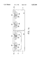
- FIGS. 1a to 1e respectively, show schematically cross-sectional views of the high-voltage metal-gate CMOS devices fabricated in the process in accordance with a preferred embodiment of the present invention as depicted in selected process stages, wherein the left hand side shows an NMOS transistor and the right hand side shows a PMOS transistor.
- FIGS. 1a to 1e A preferred embodiment of the process in accordance with the present invention for fabricating a high-voltage metal-gate CMOS device with precision alignment and dimensional symmetry is described below by referring to FIGS. 1a to 1e.
- the process of the present invention may be applicable to a semiconductor substrate of a first conductivity type with a well region of a second conductivity type (e.g. a P-type substrate with an N-type well region or an N-type substrate with a P-type well region), although it is an N-type substrate 1 employed for the description.
- the inventive process is described, the steps for fabricating both the NMOS and PMOS transistors of the CMOS device configuration are simultaneously exemplified.
- NMOS and PMOS transistors that constitute the complementary pair are fabricated on the same substrate, if an N-type substrate 1 is employed, as in the case of the exemplified embodiment depicted in the drawings, then for the NMOS transistor, a P-well 2 will have to be prepared by a conventional implanting process. On the other hand, no corresponding N-well is required for the PMOS transistor.
- a barrier layer 10 is formed on the semiconductor substrate 1 of the first conductivity type with a well region 2 of the second conductivity type.
- an oxide layer 10 is formed by thermal oxidation on an N-type substrate 1 with a P-type well region 2.
- the barrier layer 10 is patterned by conventional lithography and etching processes to form openings 12 and 14 which expose portions of the semiconductor substrate 1 and the well region 2 for prospective source/drain regions. Then, through the openings 12 and 14 respectively, low concentrations of impurities of the first conductivity type are implanted into the position 16 of the well region 2 and impurities of the second conductivity type are implanted into the position 18 of the semiconductor substrate 1.
- N-type impurities such as phosphoric ions are first implanted into the P-type well region 2.
- P-type impurities such as boron ions are implanted into the N-type substrate 1.
- a first thermal treatment is performed to drive-in the implanted low concentration of impurities. Therefore, N - lightly doped source/drain regions 16 and P - lightly doped source/drain regions 18 are formed in the P-type well region 2 and the N-type substrate 1, respectively. Meanwhile, an oxide layer 19 is also formed within the openings 12 and 14. Subsequently, a sidewall spacer 21 is formed on the sidewalls of the openings 12 and 14. For example, an oxide layer is first formed by chemical vapor deposition (CVD). That oxide layer is then etched back by reactive ion etching (RIE) to form the sidewall spacer 21.
- CVD chemical vapor deposition
- RIE reactive ion etching
- N-type impurities such as arsenic ions are first implanted into the position 22 of the N - lightly doped source/drain regions 16.
- P-type impurities such as boron ions are implanted into the position 24 of the P - lightly doped source/drain regions 18.
- the sidewall spacer 21 is removed by a conventional etching process.
- a second thermal treatment is performed to drive-in the implanted high concentration of impurities. Therefore, N + heavily doped source/drain regions 22 and P + heavily doped source/drain regions 24 are formed in the N - lightly doped source/drain regions 16 and the P - lightly doped source/drain regions 18, respectively. Meanwhile, the thickness of the oxide layer 19 is increased due to the second thermal treatment.
- the barrier layer 10 is patterned by lithography and etching processes to form openings 25 exposing areas of the semiconductor substrate 1 and the well region 2 for the prospective gate electrode.
- a gate oxide layer 27 with a thickness of between 200 ⁇ to 1000 ⁇ is formed within the openings 25 by thermal oxidation or CVD. Again, the thickness of the oxide layer 19 is increased.
- the oxide layer 19 is patterned by lithography and etching processes to form contact openings 29 exposing the heavily doped source/drain regions 22 and 24.
- a metal layer such as an aluminum layer, is sputtered on the surface of substrate.
- the metal layer is then patterned by etching to form a metal gate electrode 31a and metal lines 31b, wherein the metal gate electrode 31a is over the gate oxide layer 27.
- the metal lines 31b are connected to the heavily doped source/drain regions 22 and 24 through the contact openings 29.
Abstract
A method of fabricating a high-voltage metal-gate CMOS device is disclosed. First, a semiconductor substrate of a first conductivity type having a well region of a second conductivity type is provided. Next, a barrier layer is formed and patterned to form openings for prospective source/drain regions. Then, through the openings, low concentrations of impurities of the first conductivity type and the second conductivity type are implanted into the well region and the semiconductor substrate, respectively. After performing a first thermal treatment, lightly doped source/drain regions of the first conductivity type and the second conductivity type are formed respectively, wherein an oxide layer is also formed within the openings. A sidewall spacer is formed on the sidewalls of the openings. Then, through the openings, high concentrations of impurities of the first conductivity type and the second conductivity type are implanted into the lightly doped source/drain regions of the first conductivity type and the second conductivity type, respectively. After removing the sidewall spacer performing a second thermal treatment, heavily doped source/drain regions of the first conductivity type and the second conductivity type are formed respectively. Further, the barrier layer is patterned to expose areas of the semiconductor substrate and the well region for the prospective gate electrode. Finally, a gate oxide layer and a metal gate electrode are formed.
Description
1. Field of the Invention
This invention relates in general to the fabrication of integrated circuit (IC) devices, and more particularly to a method of fabricating a high-voltage metal-gate CMOS device having heavily doped source and drain regions that are precisely formed within the lightly doped source and drain regions, so as to guarantee the uniformity of device characteristics.
2. Description of the Prior Art
Under current technology of fabricating high-voltage CMOS devices, a polysilicon layer is normally used as the gate electrode of a CMOS device. The polysilicon gate electrode configuration, however, requires a relatively long manufacturing cycle time. Thus the manufacturing cost is raised by such a long cycle time. Furthermore, due to their inherent characteristics, CMOS devices with polysilicon gate electrodes usually encounter a latch-up problem which is fatal to the operation of the devices.
By replacing the polysilicon gate electrode with a metal gate electrode, the cycle time of manufacturing a high-voltage CMOS device can be reduced and the latch-up problem can be prevented. However, the conventional process for fabricating a high-voltage metal-gate CMOS device suffers from poor dimensional alignment and symmetry for the fabricated source/drain regions that are prerequisites for the uniformity of the electrical characteristics for these CMOS devices fabricated. These poor alignment and symmetry characteristics found in the conventional fabrication processes are inherent to the nature of the fabrication process steps employed. Poor alignment in the source and drain regions of the CMOS device result in variations of the electrical characteristics for CMOS devices produced in different production batches, as the fabrication process conditions may vary for the alignments involved in the process steps.
It is therefore an object of the present invention to provide a process for fabricating high-voltage CMOS devices having a metal gate electrode to reduce the manufacturing cycle time and prevent latch-up.
It is yet another object of the present invention to provide a process for fabricating high-voltage CMOS devices with their heavily doped source and drain regions precisely formed within the lightly doped source and drain regions in a self-aligned manner, ensuring uniformity of device characteristics.
The present invention achieves the above-identified objects by providing a method of fabricating a high-voltage metal-gate CMOS device. First, a semiconductor substrate of a first conductivity type having a well region of a second conductivity type is provided. Next, a barrier layer is formed overlying the semiconductor substrate and the well region. The barrier layer is etched to form openings exposing portions of the semiconductor substrate and the well region for prospective source/drain regions. Then, through the openings, low concentrations of impurities of the first conductivity type and the second conductivity type are implanted into the well region and the semiconductor substrate, respectively. After performing a first thermal treatment to drive-in the low concentration of impurities, lightly doped source/drain regions of the first conductivity type and lightly doped source/drain regions of the second conductivity type are formed respectively, wherein an oxide layer is also formed within the openings by the first thermal treatment. A sidewall spacer is formed on the sidewalls of the openings. Then, through the openings, high concentrations of impurities of the first conductivity type and the second conductivity type are implanted into the lightly doped source/drain regions of the first conductivity type and the lightly doped source/drain regions of the second conductivity type, respectively. After removing the sidewall spacer and performing a second thermal treatment to drive-in the high concentration of impurities, heavily doped source/drain regions of the first conductivity type and heavily doped source/drain regions of the second conductivity type are formed respectively, wherein the thickness of the oxide layer is increased. Further, the barrier layer is patterned to expose areas of the semiconductor substrate and the well region for the prospective gate electrode. A gate oxide layer is formed on the areas for the prospective gate electrode. The oxide layer is then etched to form contact openings. Finally, a metal gate electrode is formed on the gate oxide layer.
Other objects, features and advantages of the present invention will become apparent by way of the following detailed description of the preferred but non-limiting embodiment. The description is made with reference to the accompanying drawings, wherein:
FIGS. 1a to 1e, respectively, show schematically cross-sectional views of the high-voltage metal-gate CMOS devices fabricated in the process in accordance with a preferred embodiment of the present invention as depicted in selected process stages, wherein the left hand side shows an NMOS transistor and the right hand side shows a PMOS transistor.
A preferred embodiment of the process in accordance with the present invention for fabricating a high-voltage metal-gate CMOS device with precision alignment and dimensional symmetry is described below by referring to FIGS. 1a to 1e. As persons skilled in the art may well appreciate, the process of the present invention may be applicable to a semiconductor substrate of a first conductivity type with a well region of a second conductivity type (e.g. a P-type substrate with an N-type well region or an N-type substrate with a P-type well region), although it is an N-type substrate 1 employed for the description. When the inventive process is described, the steps for fabricating both the NMOS and PMOS transistors of the CMOS device configuration are simultaneously exemplified. Since the NMOS and PMOS transistors that constitute the complementary pair are fabricated on the same substrate, if an N-type substrate 1 is employed, as in the case of the exemplified embodiment depicted in the drawings, then for the NMOS transistor, a P-well 2 will have to be prepared by a conventional implanting process. On the other hand, no corresponding N-well is required for the PMOS transistor.
Stage 1
As is shown in FIG. 1a, a barrier layer 10 is formed on the semiconductor substrate 1 of the first conductivity type with a well region 2 of the second conductivity type. For example, an oxide layer 10 is formed by thermal oxidation on an N-type substrate 1 with a P-type well region 2. The barrier layer 10 is patterned by conventional lithography and etching processes to form openings 12 and 14 which expose portions of the semiconductor substrate 1 and the well region 2 for prospective source/drain regions. Then, through the openings 12 and 14 respectively, low concentrations of impurities of the first conductivity type are implanted into the position 16 of the well region 2 and impurities of the second conductivity type are implanted into the position 18 of the semiconductor substrate 1. For example, N-type impurities such as phosphoric ions are first implanted into the P-type well region 2. Then, P-type impurities such as boron ions are implanted into the N-type substrate 1.
Next, referring to FIG. 2b, a first thermal treatment is performed to drive-in the implanted low concentration of impurities. Therefore, N- lightly doped source/drain regions 16 and P- lightly doped source/drain regions 18 are formed in the P-type well region 2 and the N-type substrate 1, respectively. Meanwhile, an oxide layer 19 is also formed within the openings 12 and 14. Subsequently, a sidewall spacer 21 is formed on the sidewalls of the openings 12 and 14. For example, an oxide layer is first formed by chemical vapor deposition (CVD). That oxide layer is then etched back by reactive ion etching (RIE) to form the sidewall spacer 21. After that, through the openings 12 and 14 having the sidewall spacer 21, high concentrations of impurities of the first conductivity type and the second conductivity type are implanted into the lightly doped source/ drain regions 16 and 18 respectively. For example, N-type impurities such as arsenic ions are first implanted into the position 22 of the N- lightly doped source/drain regions 16. Then, P-type impurities such as boron ions are implanted into the position 24 of the P- lightly doped source/drain regions 18.
Stage 3
Then, as is shown in FIG. 1c, the sidewall spacer 21 is removed by a conventional etching process. A second thermal treatment is performed to drive-in the implanted high concentration of impurities. Therefore, N+ heavily doped source/drain regions 22 and P+ heavily doped source/drain regions 24 are formed in the N- lightly doped source/drain regions 16 and the P- lightly doped source/drain regions 18, respectively. Meanwhile, the thickness of the oxide layer 19 is increased due to the second thermal treatment.
Stage 4
Referring next to FIG. 1d, the barrier layer 10 is patterned by lithography and etching processes to form openings 25 exposing areas of the semiconductor substrate 1 and the well region 2 for the prospective gate electrode. Next, a gate oxide layer 27 with a thickness of between 200 Å to 1000 Å is formed within the openings 25 by thermal oxidation or CVD. Again, the thickness of the oxide layer 19 is increased.
Stage 5
As is shown in FIG. 1e, the oxide layer 19 is patterned by lithography and etching processes to form contact openings 29 exposing the heavily doped source/ drain regions 22 and 24. A metal layer, such as an aluminum layer, is sputtered on the surface of substrate. The metal layer is then patterned by etching to form a metal gate electrode 31a and metal lines 31b, wherein the metal gate electrode 31a is over the gate oxide layer 27. The metal lines 31b are connected to the heavily doped source/ drain regions 22 and 24 through the contact openings 29. This generally concludes the fabrication of the high-voltage metal-gate CMOS device comprising the NMOS and PMOS transistor pair on an N-type substrate with a P-type well region.
As is appreciable after reading the above description of the fabrication process in accordance with the exemplified preferred embodiment, persons skilled in the art may acknowledge the advantages inherent to the process of metal-gate CMOS device fabrication as disclosed by the present invention. Since the implantation of the lightly doped source/ drain regions 16 and 18 are guided by the openings 12 and 14 formed on the barrier layer 10, and the implantation of the heavily doped source/ drain regions 22 and 24 are guided by the sidewall spacer 21 formed on the sidewalls of the openings 12 and 14, the precise alignment of the heavily doped source/ drain regions 22 and 24 within the lightly doped source/ drain regions 16 and 18 can be achieved. This results in the improvement of the uniformity of the electrical characteristics of the CMOS device. Moreover, the manufacturing cycle time can be reduced since the metal gate electrode 31a and the metal lines 31b are formed in a single patterning step.
The above-described preferred embodiment of the present invention is utilized only for the purpose of the description of the present invention. Persons skilled in this art can appreciate the fact that other similar arrangements can be devised from the embodiment disclosed above without departing from the spirit of the present invention, which is recited in the following claims.
Claims (5)
1. A method of fabricating a high-voltage metal-gate CMOS device, comprising the steps of:
providing a semiconductor substrate of a first conductivity type having a well region of a second conductivity type;
forming a barrier layer overlying said semiconductor substrate and said well region, and etching said barrier layer to form openings exposing portions of said semiconductor substrate and said well region for prospective source/drain regions;
selectively implanting, through said openings, low concentrations of impurities of the first conductivity type into said well region of the second conductivity type and impurities of the second conductivity type into said semiconductor substrate of the first conductivity type;
performing a first thermal treatment to drive-in said low concentrations of impurities to form lightly doped source/drain regions of the first conductivity type and lightly doped source/drain regions of the second conductivity type respectively, wherein an oxide layer is also formed within said openings by said first thermal treatment;
forming a sidewall spacer on the sidewalls of said openings;
selectively implanting, through said openings, high concentrations of impurities of the first conductivity type into said lightly doped source/drain regions of the first conductivity type and impurities of the second conductivity type into said lightly doped source/drain regions of the second conductivity type;
removing said sidewall spacer;
performing a second thermal treatment to drive-in said high concentrations of impurities to form heavily doped source/drain regions of the first conductivity type and heavily doped source/drain regions of the second conductivity type respectively, wherein the thickness of said oxide layer is increased;
patterning said barrier layer to expose areas of said semiconductor substrate and said well region for the prospective gate electrode;
forming a gate oxide layer on said areas for the prospective gate electrode;
etching said oxide layer to form contact openings; and
forming a metal gate electrode on said gate oxide layer and forming metal lines connecting to said source/drain regions through said contact openings.
2. The method of claim 1, wherein said first conductivity type is N type and said second conductivity type is P type.
3. The method of claim 1, wherein said first conductivity type is P type and said second conductivity type is N type.
4. The method of claim 1, wherein said barrier layer is a silicon dioxide layer.
5. The method of claim 1, wherein said sidewall spacer is a silicon nitride layer.
Priority Applications (1)
| Application Number | Priority Date | Filing Date | Title |
|---|---|---|---|
| US08/490,221 US5523246A (en) | 1995-06-14 | 1995-06-14 | Method of fabricating a high-voltage metal-gate CMOS device |
Applications Claiming Priority (1)
| Application Number | Priority Date | Filing Date | Title |
|---|---|---|---|
| US08/490,221 US5523246A (en) | 1995-06-14 | 1995-06-14 | Method of fabricating a high-voltage metal-gate CMOS device |
Publications (1)
| Publication Number | Publication Date |
|---|---|
| US5523246A true US5523246A (en) | 1996-06-04 |
Family
ID=23947118
Family Applications (1)
| Application Number | Title | Priority Date | Filing Date |
|---|---|---|---|
| US08/490,221 Expired - Lifetime US5523246A (en) | 1995-06-14 | 1995-06-14 | Method of fabricating a high-voltage metal-gate CMOS device |
Country Status (1)
| Country | Link |
|---|---|
| US (1) | US5523246A (en) |
Cited By (8)
| Publication number | Priority date | Publication date | Assignee | Title |
|---|---|---|---|---|
| US5700703A (en) * | 1996-08-06 | 1997-12-23 | Motorola | Method of fabricating buried control elements in semiconductor devices |
| US6146982A (en) * | 1994-09-23 | 2000-11-14 | Infineon Technologies Ag | Method for producing a low-impedance contact between a metallizing layer and a semiconductor material |
| US6194294B1 (en) | 1998-12-22 | 2001-02-27 | Hyundai Electronics Industries Co., Ltd. | Method of forming gate electrode in semiconductor device |
| US6362058B1 (en) * | 1999-12-22 | 2002-03-26 | Texas Instruments Incorporated | Method for controlling an implant profile in the channel of a transistor |
| US6465283B1 (en) * | 2000-02-01 | 2002-10-15 | Industrial Technology Research Institute | Structure and fabrication method using latch-up implantation for improving latch-up immunity in CMOS fabrication process |
| US6583012B1 (en) | 2001-02-13 | 2003-06-24 | Advanced Micro Devices, Inc. | Semiconductor devices utilizing differently composed metal-based in-laid gate electrodes |
| US6610181B1 (en) * | 2001-04-30 | 2003-08-26 | Advanced Micro Devices, Inc. | Method of controlling the formation of metal layers |
| US9269634B2 (en) | 2011-05-16 | 2016-02-23 | Globalfoundries Inc. | Self-aligned metal gate CMOS with metal base layer and dummy gate structure |
Citations (8)
| Publication number | Priority date | Publication date | Assignee | Title |
|---|---|---|---|---|
| JPS5324280A (en) * | 1976-08-19 | 1978-03-06 | Sony Corp | Production of semiconductor integrated circuit |
| JPH01133365A (en) * | 1987-11-18 | 1989-05-25 | Sanyo Electric Co Ltd | Manufacture of mos semiconductor device |
| US4851257A (en) * | 1987-03-13 | 1989-07-25 | Harris Corporation | Process for the fabrication of a vertical contact |
| JPH02122648A (en) * | 1988-11-01 | 1990-05-10 | Fujitsu Ltd | Manufacture of semiconductor device |
| US5075242A (en) * | 1988-12-19 | 1991-12-24 | Kabushiki Kaisha Toshiba | Method of manufacturing CMOS semiconductor device having decreased diffusion layer capacitance |
| JPH0471236A (en) * | 1990-07-11 | 1992-03-05 | Nec Corp | Manufacture of semiconductor device |
| US5342794A (en) * | 1992-09-10 | 1994-08-30 | Vlsi Technology, Inc. | Method for forming laterally graded deposit-type emitter for bipolar transistor |
| US5439834A (en) * | 1994-11-15 | 1995-08-08 | Winbond Electronics Corp. | Method for fabricating a CMOS device with reduced number of photolithography steps |
-
1995
- 1995-06-14 US US08/490,221 patent/US5523246A/en not_active Expired - Lifetime
Patent Citations (8)
| Publication number | Priority date | Publication date | Assignee | Title |
|---|---|---|---|---|
| JPS5324280A (en) * | 1976-08-19 | 1978-03-06 | Sony Corp | Production of semiconductor integrated circuit |
| US4851257A (en) * | 1987-03-13 | 1989-07-25 | Harris Corporation | Process for the fabrication of a vertical contact |
| JPH01133365A (en) * | 1987-11-18 | 1989-05-25 | Sanyo Electric Co Ltd | Manufacture of mos semiconductor device |
| JPH02122648A (en) * | 1988-11-01 | 1990-05-10 | Fujitsu Ltd | Manufacture of semiconductor device |
| US5075242A (en) * | 1988-12-19 | 1991-12-24 | Kabushiki Kaisha Toshiba | Method of manufacturing CMOS semiconductor device having decreased diffusion layer capacitance |
| JPH0471236A (en) * | 1990-07-11 | 1992-03-05 | Nec Corp | Manufacture of semiconductor device |
| US5342794A (en) * | 1992-09-10 | 1994-08-30 | Vlsi Technology, Inc. | Method for forming laterally graded deposit-type emitter for bipolar transistor |
| US5439834A (en) * | 1994-11-15 | 1995-08-08 | Winbond Electronics Corp. | Method for fabricating a CMOS device with reduced number of photolithography steps |
Cited By (8)
| Publication number | Priority date | Publication date | Assignee | Title |
|---|---|---|---|---|
| US6146982A (en) * | 1994-09-23 | 2000-11-14 | Infineon Technologies Ag | Method for producing a low-impedance contact between a metallizing layer and a semiconductor material |
| US5700703A (en) * | 1996-08-06 | 1997-12-23 | Motorola | Method of fabricating buried control elements in semiconductor devices |
| US6194294B1 (en) | 1998-12-22 | 2001-02-27 | Hyundai Electronics Industries Co., Ltd. | Method of forming gate electrode in semiconductor device |
| US6362058B1 (en) * | 1999-12-22 | 2002-03-26 | Texas Instruments Incorporated | Method for controlling an implant profile in the channel of a transistor |
| US6465283B1 (en) * | 2000-02-01 | 2002-10-15 | Industrial Technology Research Institute | Structure and fabrication method using latch-up implantation for improving latch-up immunity in CMOS fabrication process |
| US6583012B1 (en) | 2001-02-13 | 2003-06-24 | Advanced Micro Devices, Inc. | Semiconductor devices utilizing differently composed metal-based in-laid gate electrodes |
| US6610181B1 (en) * | 2001-04-30 | 2003-08-26 | Advanced Micro Devices, Inc. | Method of controlling the formation of metal layers |
| US9269634B2 (en) | 2011-05-16 | 2016-02-23 | Globalfoundries Inc. | Self-aligned metal gate CMOS with metal base layer and dummy gate structure |
Similar Documents
| Publication | Publication Date | Title |
|---|---|---|
| US5283455A (en) | Thin film field effect element having an LDD structure | |
| US7276407B2 (en) | Method for fabricating semiconductor device | |
| US5294822A (en) | Polycide local interconnect method and structure | |
| US6174778B1 (en) | Method of fabricating metal oxide semiconductor | |
| US5612240A (en) | Method for making electrical connections to self-aligned contacts that extends beyond the photo-lithographic resolution limit | |
| US20090014789A1 (en) | Semiconductor device and method for manufacturing the same | |
| US5851865A (en) | Method of manufacturing semiconductor device having mask layer forming step for ion implantation | |
| US7468297B2 (en) | Method of manufacturing semiconductor device | |
| JP2001156290A (en) | Semiconductor device | |
| US5523246A (en) | Method of fabricating a high-voltage metal-gate CMOS device | |
| US6218229B1 (en) | Method of fabricating semiconductor device having a dual-gate | |
| US7148096B2 (en) | Method of manufacturing a semiconductor device having a gate electrode containing polycrystalline silicon-germanium | |
| US5518938A (en) | Process for fabricating a CMOS transistor having high-voltage metal-gate | |
| JP2596117B2 (en) | Method for manufacturing semiconductor integrated circuit | |
| JP2667282B2 (en) | Semiconductor device and wiring forming method thereof | |
| JPH10335484A (en) | Manufacture of semiconductor device | |
| JPH04251980A (en) | High withstand-voltage transistor and its manufacture | |
| JPH0738095A (en) | Semiconductor device and its manufacturing method | |
| US6232162B1 (en) | Method of complementary metal-oxide semiconductor | |
| KR20010066327A (en) | A method for fabricating dual gate electrode | |
| US6013554A (en) | Method for fabricating an LDD MOS transistor | |
| US5789287A (en) | Method of forming field isolation in manufacturing a semiconductor device | |
| US6753573B2 (en) | Semiconductor device having complementary MOS transistor | |
| JPH07297397A (en) | Manufacture of semiconductor device | |
| JP2000200903A (en) | Manufacture of semiconductor device |
Legal Events
| Date | Code | Title | Description |
|---|---|---|---|
| AS | Assignment |
Owner name: UNITED MICROELECTRONICCS CORPORATION, TAIWAN Free format text: ASSIGNMENT OF ASSIGNORS INTEREST;ASSIGNOR:YANG, SHENG-HSING;REEL/FRAME:007565/0036 Effective date: 19950525 |
|
| STCF | Information on status: patent grant |
Free format text: PATENTED CASE |
|
| FPAY | Fee payment |
Year of fee payment: 4 |
|
| FEPP | Fee payment procedure |
Free format text: PAYOR NUMBER ASSIGNED (ORIGINAL EVENT CODE: ASPN); ENTITY STATUS OF PATENT OWNER: LARGE ENTITY |
|
| FPAY | Fee payment |
Year of fee payment: 8 |
|
| FPAY | Fee payment |
Year of fee payment: 12 |