US5515452A - Optical character recognition illumination method and system - Google Patents
Optical character recognition illumination method and system Download PDFInfo
- Publication number
- US5515452A US5515452A US07/999,294 US99929492A US5515452A US 5515452 A US5515452 A US 5515452A US 99929492 A US99929492 A US 99929492A US 5515452 A US5515452 A US 5515452A
- Authority
- US
- United States
- Prior art keywords
- radiation
- angle
- incident
- radiation source
- region
- Prior art date
- Legal status (The legal status is an assumption and is not a legal conclusion. Google has not performed a legal analysis and makes no representation as to the accuracy of the status listed.)
- Expired - Lifetime
Links
Images


Classifications
-
- G—PHYSICS
- G06—COMPUTING; CALCULATING OR COUNTING
- G06K—GRAPHICAL DATA READING; PRESENTATION OF DATA; RECORD CARRIERS; HANDLING RECORD CARRIERS
- G06K7/00—Methods or arrangements for sensing record carriers, e.g. for reading patterns
- G06K7/10—Methods or arrangements for sensing record carriers, e.g. for reading patterns by electromagnetic radiation, e.g. optical sensing; by corpuscular radiation
- G06K7/10544—Methods or arrangements for sensing record carriers, e.g. for reading patterns by electromagnetic radiation, e.g. optical sensing; by corpuscular radiation by scanning of the records by radiation in the optical part of the electromagnetic spectrum
- G06K7/10554—Moving beam scanning
- G06K7/10564—Light sources
- G06K7/10574—Multiple sources
-
- G—PHYSICS
- G06—COMPUTING; CALCULATING OR COUNTING
- G06K—GRAPHICAL DATA READING; PRESENTATION OF DATA; RECORD CARRIERS; HANDLING RECORD CARRIERS
- G06K7/00—Methods or arrangements for sensing record carriers, e.g. for reading patterns
- G06K7/10—Methods or arrangements for sensing record carriers, e.g. for reading patterns by electromagnetic radiation, e.g. optical sensing; by corpuscular radiation
- G06K7/14—Methods or arrangements for sensing record carriers, e.g. for reading patterns by electromagnetic radiation, e.g. optical sensing; by corpuscular radiation using light without selection of wavelength, e.g. sensing reflected white light
-
- G—PHYSICS
- G06—COMPUTING; CALCULATING OR COUNTING
- G06V—IMAGE OR VIDEO RECOGNITION OR UNDERSTANDING
- G06V10/00—Arrangements for image or video recognition or understanding
- G06V10/10—Image acquisition
- G06V10/12—Details of acquisition arrangements; Constructional details thereof
- G06V10/14—Optical characteristics of the device performing the acquisition or on the illumination arrangements
- G06V10/145—Illumination specially adapted for pattern recognition, e.g. using gratings
-
- H—ELECTRICITY
- H01—ELECTRIC ELEMENTS
- H01L—SEMICONDUCTOR DEVICES NOT COVERED BY CLASS H10
- H01L23/00—Details of semiconductor or other solid state devices
- H01L23/544—Marks applied to semiconductor devices or parts, e.g. registration marks, alignment structures, wafer maps
-
- H—ELECTRICITY
- H01—ELECTRIC ELEMENTS
- H01L—SEMICONDUCTOR DEVICES NOT COVERED BY CLASS H10
- H01L2223/00—Details relating to semiconductor or other solid state devices covered by the group H01L23/00
- H01L2223/544—Marks applied to semiconductor devices or parts
- H01L2223/54406—Marks applied to semiconductor devices or parts comprising alphanumeric information
-
- H—ELECTRICITY
- H01—ELECTRIC ELEMENTS
- H01L—SEMICONDUCTOR DEVICES NOT COVERED BY CLASS H10
- H01L2223/00—Details relating to semiconductor or other solid state devices covered by the group H01L23/00
- H01L2223/544—Marks applied to semiconductor devices or parts
- H01L2223/54453—Marks applied to semiconductor devices or parts for use prior to dicing
-
- H—ELECTRICITY
- H01—ELECTRIC ELEMENTS
- H01L—SEMICONDUCTOR DEVICES NOT COVERED BY CLASS H10
- H01L2223/00—Details relating to semiconductor or other solid state devices covered by the group H01L23/00
- H01L2223/544—Marks applied to semiconductor devices or parts
- H01L2223/54493—Peripheral marks on wafers, e.g. orientation flats, notches, lot number
-
- H—ELECTRICITY
- H01—ELECTRIC ELEMENTS
- H01L—SEMICONDUCTOR DEVICES NOT COVERED BY CLASS H10
- H01L2924/00—Indexing scheme for arrangements or methods for connecting or disconnecting semiconductor or solid-state bodies as covered by H01L24/00
- H01L2924/0001—Technical content checked by a classifier
- H01L2924/0002—Not covered by any one of groups H01L24/00, H01L24/00 and H01L2224/00
Definitions
- the present invention relates to the field of optical character recognition, and more specifically to an optical character recognition illumination method and apparatus for use in recognizing characters on a semiconductor wafer.
- an image containing characters is acquired and processed by special hardware and software that can identify the characters.
- a camera may focus the image of an area of an object having the characters on some type of imaging array. The camera acquires an image of the character. The image is then processed by hardware and software which can identify the characters.
- the characters can be numbers, letters, special symbols or any other similar marking such as a bar code, for example.
- FIG. 1 shows a portion of semiconductor wafer 100 having a six character wafer ID 101. Often, as shown in FIG. 1, wafer ID 101 is placed near a flat 102 of the wafer. As is well known, wafer ID 101 may comprise a greater or lesser number of characters. The wafer ID 101 can be numbers, letters, special symbols or markings, or a combination of any or all of these.
- region 140 is the area which will be focused by the camera on the imaging array and examined by the optical character recognition system.
- Field 140a is used to denote all of region 140 except for the characters of wafer ID 101.
- the surface of semiconductor wafer 100 in the field 140a is highly reflective and is generally considered mirror-like. Therefore, light incident on field 140a reflects light specularly, and the angle of incidence equals the angle of reflection.
- the characters of wafer ID 101 must therefore either absorb light, reflect light in a different direction than light reflected from the field 140a or scatter light in order to generate contrast so that they can be read.
- the wafer ID 101 is scribed on wafer 100 via laser. While the surface of wafer 100 in the region of the characters may remain highly reflective on the scale of the wavelength used to read the characters, the characters present an uneven surface so that incident light is reflected in many directions compared to light reflecting from the planar surface of wafer 100 in other regions.
- Figures herein show scribe marks which have smooth, even surfaces which reflect light specularly at a different angle from the surface of wafer 100, at least some portions of the scribe mark are typically roughened on a microscopic scale, so that light incident on these portions is scattered in all directions.
- scribing wafer ID 101 on semiconductor wafer 100 There are many methods of scribing wafer ID 101 on semiconductor wafer 100.
- One method referred to as hard mark or hard scribe, scribes a relatively deep trench (typically a few to several microns deep)into the surface of semiconductor wafer 100.
- FIG. 2A a cross-sectional elevation view of semiconductor wafer 100 is shown. Scribe mark 201 could be for example a hard mark and forms a portion of one of the characters of wafer ID 101.
- the characters of wafer ID 101 are made up of individual roughly circular scribe marks and thus are similar to dot matrix type characters.
- the characters of wafer ID 101 may be made of one or more long continuous trenches. As shown in FIG.
- scribe mark 201 has a kerr 202 surrounding the outer edges of trench 203.
- incident light 210 strikes the surface of wafer 100 at an angle of 90 degrees (perpendicularly). Since the surface of wafer 100 surrounding wafer ID 101 (i.e., the field 140a) is smooth and highly reflective, the angle of incidence equals the angle of reflection, and nearly all of incident light 210 is reflected straight back along the same path of the incident light rays 210 as shown by reflected light 211 (shown separated from incident light 210 for clarity).
- the reflected light such as reflected light 215 and 218 is reflected in widely varying directions, depending upon the portion of scribe mark 201 which it hits.
- the angle of incidence and angle of reflection are measured from the normal to the surface.
- the angle of reflection 217 equals the angle of incidence 216 at the point on the wafer where incident light 210 strikes.
- this surface is at an angle compared to the plane of the surface of wafer 100 and field 140a.
- FIG. 2B shows the same cross-sectional view in FIG. 2B, however, incident light rays 220 strike the field 140a at an angle 222 of less than 90°.
- the reflected light 221 leaves the surface at an angle 223 which, because the surface is highly reflective and smooth, is equal to the angle of incidence 222.
- some of incident light 220 is shown striking the surface of trench 203.
- the angle of reflection 227 for the reflected light 225 is equal to the angle of incidence 226 at the point the light strikes in trench 203 for some of incident light 220.
- FIG. 2B shows a smooth surface in the region of scribe mark 201.
- the surface on a microscopic scale may be very rough or faceted. This still has the same effect as discussed in relation to FIG. 2A, namely, that the incident radiation in the scribe mark 201 gets reflected and/or scattered in all directions, with only a small, random portion being reflected in the direction of reflected light from the field 140a.
- marks such as scribe mark 201 having large features out of the plane of the field 140a such as kerf 202 and trench 203, much of the light is reflected at high angles relative to the plane of the field 140a. Stated in another way, with marks such as scribe mark 201, it can be expected that at a large angle away from the angle of reflection of the field 140a, where little or no light reflected from the field 140a will be detected, there will be a significant amount of reflected/scattered radiation detected from the scribe mark 201.
- FIG. 2C shows the same cross-sectional view as FIGS. 2A and 2B.
- incident light 230 strikes the field and the scribe mark 201 at a very glancing angle 232.
- Reflected light 231 from the field 140a is reflected at an equal angle of reflection 233.
- much of incident light 230 striking the scribe mark 201 is reflected at a high angle relative to the plane of the field 140a. Because light is reflected off of scribe mark 201 at a high angle, when the region 140 is illuminated with incident light 230 at glancing angle 232, much of the light is scattered or reflected upward.
- the field 140a will appear dark (since most reflected light 231 is reflected in direction 231 ).
- the characters will appear bright due to the light reflected and/or scattered upward. This method of illumination is known as dark field illumination.
- FIG. 3 shows two of scribe marks 301 on semiconductor wafer 100.
- Scribe marks 301 could be, for example, soft scribe marks.
- the trenches 303 of the scribe marks 301 are shallower than for the mark 201 of FIG. 2. Additionally the kerf 302 is smaller.
- Incident light 310 strikes the field 140a of semiconductor wafer 100 at an angle 312 relative to the surface of the field 140a. Reflected light 311 from the field 140a is reflected at an angle of incidence 312.
- Light reflected from the scribe marks 301, such as reflected light 315 and 316 is shown together with arrows 31la, which show the direction of reflected light 311 from the field 140a.
- the method often used to read such characters is the bright field illumination described above.
- incident light is directed at the characters from directly above such as incident light 210.
- a detector such as a camera is placed directly above the characters.
- the incident light 210 is typically a collimated light beam which is injected into the optical path coaxially by use of a beam splitter.
- the illumination is referred to as coaxial because the illuminating light travels the same path as the reflected light which is detected.
- the field 140a reflects all incident radiation back, while scribe marks 201, which make up the characters, reflect in all directions. This gives rise to good contrast allowing the characters to be easily read.
- the scribe marks 301 do not give rise to a significant degree of scattering. Because of this, if a coaxial bright field beam is used, the field will appear only slightly brighter than the characters. That is, the contrast is relatively poor. Thus the coaxial method used for reading a character with scribe marks such as scribe mark 201 cannot be used to read a character composed of scribe marks such as scribe mark 301.
- markings 125 and 130 are shown.
- the markings from an edge bead removal process look like rings or bands as shown.
- there is often discoloration or regions of differing color between the rings for example between ring 125 and 130.
- the markings from the edge bead removal process do not appear to give rise to much scattering.
- the markings such as line 125 and 130 have a different reflectivity than the surrounding surface and can confuse the optical character recognition process.
- line 130 may make the C in wafer ID 101 look like an E when observed with bright field illumination.
- optical character recognition illumination A further problem with optical character recognition illumination is that light from the environment in which the optical character recognition is taking place illuminates the wafer from all directions. This tends to reduce contrast in most cases.
- What is needed is a single system which can provide illumination such that all types of scribe marks can be read. Further, the system should be able to read scribe marks which have partially obscured characters due to, for example, markings due to edge bead removal processes. The system should have a reduced sensitivity to environmental lighting. Finally, the system should not require costly and complicated optics such as lenses, beam splitters, etc.
- An apparatus and method for illuminating characters to be read by an optical character recognition system is disclosed.
- a first light source strikes the surface at an angle of incidence, the angle of incidence being greater than 0°.
- a detector is placed at the angle of reflection, to provide non-coaxial bright field illumination.
- Embodiments the invention including additional light sources are disclosed.
- the additional light sources provide light at an angle other than the angle of reflection, to provide for dark field illumination. Further provided are novel, inexpensive light guides, methods and apparatus for reduced sensitivity to environmental lighting, and a novel method of determining the optimum light source and intensity level.
- FIG. 1 shows a plan view of a portion of a semiconductor wafer with a wafer ID thereon.
- FIGS. 2A, 2B and 2C illustrate the reflection of incident light from a wafer having a hard mark type scribe.
- FIG. 3 illustrates the reflection of light from a wafer having a soft mark type scribe.
- FIG. 4 illustrates the non-coaxial bright field illumination of the present invention.
- FIGS. 5A and 5B show a preferred embodiment of the bright field illumination light guide of the present invention.
- FIGS. 6A and 6B show a preferred embodiment of the dark field illumination light guide of the present invention.
- FIG. 7 shows a currently preferred embodiment of the light source configuration of the present invention.
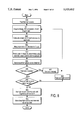
- FIG. 8 shows a flow chart in a currently preferred embodiment of the light source and intensity selection of the present invention.
- FIG. 9 shows a representation of a pixel data structure in a currently preferred embodiment of the present invention.
- FIG. 10 shows a representation of a projection of each row in the pixel data struction of FIG. 9.
- OCR optical character recognition
- incident light 400 from light guide 405 strikes the surface of semiconductor wafer 100 at an angle 410.
- Light guide 405 will be described in more detail below in conjunction with FIG. 5.
- angle 410 is approximately 85 degrees.
- Reflected light 415 from the field 140a is reflected at an angle 411, equal to the angle of incidence 410, or approximately 85 degrees in a currently preferred embodiment.
- Detector 420 is positioned at the angle of reflection as shown.
- Detector 420 could be, for example, a camera which focuses an image of region 140 on an imaging array. Referring back to FIG. 2B, and the discussion thereof, it can be seen that light striking the planar field 140a will be directed into detector 420. However, light striking a scribe mark 201 will be scattered in many directions such as 225 and 228 of FIG. 2B. The incident light which is scattered from characters of wafer ID 101 is shown as 425 in FIG. 4. In detector 420, incident radiation 400 which strikes the field 140a of wafer 100 will be reflected into detector 420, and the field 140a will appear bright. Light striking the characters made of scribe marks 201 will be scattered so that only a small portion thereof will strike the detector 420.
- the apparatus and method illustrated in FIG. 4 is the bright field illumination described in the background section. It should be noted that use of a light guide providing incident radiation at an angle of incidence 410, and providing a detector at the angle of reflection 411, provides for bright field illumination in essentially the same manner as the coaxial system described earlier. However, the embodiment of the present invention shown in FIG. 4 has the advantage that no collimating lenses or beam splitters, for example, are required. In addition, since the light beam of the present invention is not highly collimated, more of the light reaches region 140, resulting in greater contrast.
- FIG. 5A shows bright field light guide 405 of the present invention.
- bright field light guide 405 has a length 511 in the range of approximately 11/2-3 inches.
- the width 514 of light guide 405 is in the range of approximately 2-3 inches.
- Light guide 405 comprises two legs 503, each having a length 513 of approximately 1/2 inch.
- the distance between the legs 503 is approximately 1 1/2 inches.
- the height 510 is in the range of approximately 1/2-1 inch.
- light guide 405 comprises five light emitting diodes (LEDs) 501.
- the five LEDs are mounted on a printed circuit board (PCB) assembly which is attached to the legs 513 of light guide 405.
- the PCB is mounted such that the LEDs 501 fit in ports provided in light guide 405.
- PCB printed circuit board
- LEDs used for bright field illumination are high power lens end, red LEDs of the AlGaAs (aluminum gallium arsenide) type. These types of LEDs have a lens, which focuses the light such that it is emitted in a solid angle of approximately 0.01 steradians.
- Light from the LEDs 501 travels through light guide 405 and strikes diffuse reflecting surface 502 which is at an angle of 45 degrees from the top surface of light guide 405 in a currently preferred embodiment.
- the light guide 405 channels most light from the LEDs 501 to the reflecting surface 502 by total internal reflection.
- light guide 405 is made of optical grade acrylic. Alternatively, glass, or other optical grade plastics can be used.
- the legs 503 of light guide 405 are used to mount the LED bar within the light guide 405, as described above, as well as to mount the light guide in the optical character recognition illumination system.
- the light guide 405 is highly transmissive, so that only a small fraction of the light from light emitting diodes is lost.
- FIG. 5B shows a front, head-on view of light guide 405.
- the light beam 520 emitted from surface 502 fans out slightly (approximately 15 degrees).
- the light beam 520 is shown shining on the surface of semiconductor wafer 100 in the region 140.
- the characters making up wafer ID 101 run right to left or left to right as shown by arrow 521.
- the light is not collimated in the direction 521. Thus there is no loss of intensity due to collimation in this direction.
- the side view of light guide 405 is shown. Due to the lenses in the LED light sources, as well as the collimation provided by the light travel through light guide 405, the light is partially collimated in the direction shown as 421.
- the light beam 400 of FIG. 4 fans out approximately 5 degrees. This amount of collimation is acceptable for optical character recognition.
- FIG. 6A shows dark field light guide 600.
- dark field guide 600 is made of optical grade acrylic.
- the length 611 of light guide 600 is in the range of approximately 1 1/2-3 inches.
- the width 614 of light guide 600 is in the range of approximately 1 1/2-2 inches.
- the height 610 of light guide 600 is in the range of 1/4-1/2 inch.
- Light guide 600 has two legs 603, which are each approximately 1/2 inch long in a currently preferred embodiment. All surfaces of light guide 600 are polished for high reflectivity.
- Light guide 600 comprises five light emitting diodes 601 which provide the illumination. In a currently preferred embodiment, light guide 600 uses the same type of LEDs as the LEDs 501 in light guide 405.
- the front end of light guide 600 comprises two tapered edges 602 which are tapered at an angle of approximately 15° relative to the top and bottom surfaces for a distance 612 of approximately 3/4 inch. As light travels through the light guide 600 it is reflected off the surfaces by total internal reflection and is emitted from the face 613 of light guide 600 in a relatively flat beam of light. Face 613 has a dimension 615 of approximately 1/8 inch.
- FIG. 6B shows a side view of light guide 600. One ray 630 of light is shown coming from light emitting diode 601, reflecting off the left tapered edge 602 and exiting face 613. The beam 625 from light guide 600 is confined to approximately 5 degrees. With both light guides 405 and 600, although the light fans out approximately 5 degrees, the light in the center of the beam, which is aimed at region 140, is the most intense portion of the beam.
- LEDs 501 and 601 are used as a light source, the effect of room light on image contrast can be eliminated.
- the previously mentioned LEDs 501 and 601 emit light of a wavelength in the range of approximately 640-660 nm.
- a band pass filter is used in the detector which passes wavelengths greater than approximately 630 nm and which prevents all other wavelengths from reaching the detector.
- room lighting comprises significant amounts of light near the blue end of the spectrum, and only small portions near the wavelengths emitted by the LEDs and passed by the filter. Thus, there is very little extraneous light at the detection wavelength. Therefore, room lighting has very little effect on image contrast.
- FIG. 7 shows illumination system 700 according to the present invention which provides illumination for nearly all types of scribe marks encountered.
- bright field assembly 701 with bright field light guide 405 is used for bright field illumination of the wafer.
- Dark field high angle assembly 702 with dark field light guide 600 is used for dark field illumination which strikes the regions 140 at a relatively high angle.
- Dark field low angle light assembly 703 with dark field light guides 600 are used for dark field illumination which strikes the region 140 at a relatively low angle.
- only one type of lighting is used at a time. While the embodiment described herein utilizes one bright field assembly 701, one dark field high angle assembly 702, and two dark field low angle assemblies 703, it will be understood that configurations having a greater or a lesser number of any of these assemblies may be employed.
- dark field low angle assemblies 703 could be eliminated if this type of illumination is not needed for a particular application.
- the light guides 405 and 600 have been described as having five LEDs, the number of LEDs may be varied depending upon the particular requirements of a given application.
- bright field assembly 701 is used for bright field lighting. That is, incident light 710 strikes the region 140 of wafer 100 at an angle 712 of approximately 85 degrees in a currently preferred embodiment.
- the reflected light 711 from the field 140a of semiconductor wafer 100 is reflected at an angle 713 equal to angle 712.
- camera 750 is positioned at this angle 713 so that reflected light 711 strikes the lens 751 of camera 750, and is focused on the imaging array in the region examined by the OCR system, making the field appear bright.
- light from characters present in the region 140 is widely scattered. Thus the characters appear dark in comparison to the field 140a.
- this type of lighting scheme would be used, for example, for scribe mark 201 of FIG. 2B.
- High angle dark field assembly 702 with light guide 600 emits incident light 720 at an angle 722 of approximately 10° in a currently preferred embodiment.
- Light guide assembly 702 can be adjusted in the direction shown as 725, such that the angle at which it strikes wafer 100 in the region 140 can be varied from approximately 0° to 30°.
- camera 750 is positioned at an angle equal to the angle 712 of reflected light 711. Since high angle dark field light 720 hits the wafer at a different angle, specularly reflected light 721 strikes the lens 751 of camera 750 well away from the center of the lens, and is focused on the imaging array in a region not examined by the OCR system. Therefore in the region examined by the OCR system, the field 140a in the region 140 appears dark. Referring to FIG.
- low angle light sources 703. In a currently preferred embodiment two of such light sources 703 are used. As can be seen, the light beam 730 coming from light sources 703 strike wafer 100 at a very low angle. Thus, light reflected specularly from the field 140a in the region 140 is reflected at the same glancing angle and will not reach camera 750. However, for scribe marks such as scribe mark 201 of FIGS. 2, light striking the scribe mark 201 will be scattered at high angles in all directions, as discussed in conjunction with FIG. 2C. Thus, a significant amount of incident light 730 which strikes the characters of the wafer ID 101, such as reflected light 275 of FIG. 2C, will be reflected directly up into the camera.
- the field 140a will appear dark while the characters appear bright due to the scattered light.
- the light sources 703 are used, for example, on wafers with the edge bead problem described in relation to FIG. 1.
- the edge bead removal marks do not give rise to much high angle scattering. Rather, they are of differing reflectivity. Thus, light striking the edge bead marks in the field will be specularly reflected, (although attenuated) but not significantly scattered toward the camera. Therefore, most scattered light reaching the camera will be that coming from the characters. Therefore the edge bead removal marks will cause no change in the contrast allowing for reading of wafers with edge bead removal marks.
- wafer IDs 101 having similar marks, such as thin films of deposited materials or organic materials, which may obscure the marks due to differing reflectivity or absorption characteristics, but which do not give rise to significant high angle scattering, can be read using light source 703.
- band pass filter 752 As mentioned previously, this filter allows only those wavelengths of light at which the LED 501 and 601 emit light. Therefore any stray light of other wavelengths striking either the field or the characters from other directions from other sources in the environment will not reach the imaging array of camera 750.
- the selection of which of the light sources shown in FIG. 7 and the light intensity to be used on a wafer to be identified can be done manually by an operator, or can be performed automatically.
- the effectiveness of a light source or intensity is often determined by scanning the entire field and using the source or intensity giving the highest overall contrast in the field.
- the present invention provides a novel method for determining which source gives the best contrast, and consequently the best accuracy, by examining only the top and bottom edges of the characters.
- the method of the present invention is illustrated in conjunction with FIGS. 8, 9 and 10.
- a first light source is selected to be tested. This could be any one of assemblies 701, 702, or 703 of FIG. 7.
- the image is acquired.
- an analog to digital conversion is performed wherein a pixel data structure having 6 bit location (64 gray scale levels) for each pixel is created. If one of the previously described dark field illumination methods is used, the image is inverted by reversing polarity on the A to D converter. Thus, in the data structure, all images appear as bright field images. A portion of the data structure is shown in FIG. 9. A zero is placed in each location which has a low intensity. Although as stated above each pixel is one of 64 gray levels, for simplicity the method of the present invention will be discussed in terms of a single bit pixel being either off or on. It will be obvious to one skilled in the art how the method of the present invention is carried out on data structures having pixels with any number of gray levels. All regions where no zero appears are assumed to be one.
- FIG. 9 a portion of region 140 is shown. As can be seen in row number one in the section shown, there are no zeros (dark pixels). Of course, to the right of the region shown in the Figure there may be some dark pixels in this row. It will be understood that FIG. 9 shows only a portion of the region 140 examined by the present method. Next, as can be seen in the Figure, row two contains a couple of dark pixels. These could be due to blemishes on the surface of wafer 100, noise in the data, or other factors causing the pixel to be dark. As can be seen, starting at row five there are several pixels in a row which are dark. Similarly row 6-10 have several dark pixels.
- the group of dark pixels 905 could be, for example, the top of a letter such as the letter T. It will be understood that an edge of a letter may contain more or less pixels than that shown.
- a projection for each row is calculated. That is, the intensity value of all pixels in each row is summed.
- this projection in the x direction is mapped to the y axis. The result of this is shown in FIG. 10.
- the x axis shows the number of the row corresponding to the row numbers in FIG. 9.
- the y axis gives a value of the combined pixel intensity for all pixels in each row. As can be seen, both the left and right sides of curve 1000 have high values.
- a pair of edges is found.
- an edge intensity for each row is calculated.
- the edge intensity for each row is equal to the difference between the combined pixel intensity for the immediately succeeding row and the combined pixel intensity for the immediately preceding row.
- the edge polarity is determined. The edge polarity is either positive or negative for a given row based upon whether the immediately succeeding row has a lesser combined pixel intensity than the immediately preceding row or a greater combined pixel intensity. For example, the row corresponding to data point 1001 of FIG.
- each edge having an edge intensity above a predetermined threshold and a positive polarity is paired with each edge having an intensity above the threshold value and a negative polarity, to form edge pairs to be assigned a score. Every edge pair is assigned a score based on the combined edge intensity value for the edge pair and the separation distance between the rows of the pair.
- each edge pair is as follows in a currently preferred embodiment: ##EQU1## where D is the separation distance between the two rows in the pair, E is the character height, Value is the combined edge intensity, and Max is the maximum possible edge intensity (i.e., the intensity value if all pixels in the succeeding row had an intensity level of 0, and all pixels in the preceeding row had an intensity level of 63, or vice versa, for the currently preferred embodiment having 64 gray levels.) As can be seen from the formula, the highest possible score is 1000.
- the pair of edges will satisfy the conditions that each row has a high edge intensity value, the two edges have opposite polarity, and there is a separation distance equal to or close to the height of the character. Referring to FIG.
- distance 1005 shows the height of the character. Therefore, the rows corresponding to the data points 1001 and 1002, may have the highest score, based upon their high edge intensity value, opposite polarities and the fact that they are separated by the distance 1005 corresponding to the height of a character.
- step 805 of FIG. 8 the highest score for a pair of edges is stored along with the light source and intensity used.
- step 806 a determination is made as to whether a different light intensity for the light source being used, should be tested in order to find the best intensity for the light source being tested.
- the various light sources have 256 intensity levels.
- step 806 a new intensity will be tested until a peak intensity (intensity giving highest score through steps 801 through 805) for the light source being tested is found.
- the 256 intensity levels are first stepped through in 10 equal increments (e.g., start at 55, then 75, etc.) to determine the score as a function of light intensity and to find an initial peak intensity.
- the mean pixel value and standard deviation for all pixels is determined prior to performing the steps 801-805 for an intensity level. If the mean pixel value is above or below a certain threshold, signifying that the image is almost completely bright or completely dark, or is the standard deviation is below a certain threshold, signifying poor contrast, then the intensity level is not tested through the steps 801-805 in order to save time. Each intensity level which is not eliminated as described above is tested through steps 801-805 to find a pair of edges yielding the highest score for that intensity level.
- step 806 and 807 further intensities are tested in steps 806 and 807, based upon the initial peak intensity.
- three intensity levels in increments of 6 near the initial peak are tested. For example, if the initial peak intensity had been at an intensity level of 215, and the highest score for a pair of edges appeared to be rising at that point, then intensity levels such as 215, 221 and 227 would be tested, to find an intermediate peak.
- the final peak intensity is determined in a similar manner by testing three intensity levels at or near the intermediate peak in increments of three. It will be appreciated by one skilled in the art that many different routines for determining the peak intensity can be used in the present invention.
- step 806 the score of the pair of edges having the highest score, along with the intensity value at which the highest score occurred, for the light source being tested, is stored for comparison with the highest score at peak intensity for other light sources, as described below.
- step 808 it is determined whether all light sources have been tested. If not, then, as shown by step 809 the next light source is tested, and the processing returns to step 801. If all light sources have been tested, the light source and intensity achieving the highest score is used for optical character recognition as shown by step 810. After the ID has been read, as shown by step 811 the best type of light source and intensity for that ID number is stored. For example, if for the wafer ID 101 ABC-123 shown in FIG. 1, bright field source 701 at a certain intensity level had given the highest score, then that fact could be stored in the OCR system as set up data to be used for the rest of the lot, for example.
- LEDs as a light source has a further advantage in the present invention in conjunction with the intensity selection described above.
- Prior art lighting techniques commonly require up to 50 milliseconds or more to stabilize.
- the LEDs of the present invention require only 2-4 milliseconds to stabilize. Therefore, the testing of each light source at various intensities can be carried out rapidly compared with the prior art. Therefore, all light sources and intensities can be quickly tested to determine which will give the highest accuracy, without significantly impacting throughput time.
Landscapes
- Engineering & Computer Science (AREA)
- Physics & Mathematics (AREA)
- General Physics & Mathematics (AREA)
- Electromagnetism (AREA)
- Artificial Intelligence (AREA)
- Computer Vision & Pattern Recognition (AREA)
- Theoretical Computer Science (AREA)
- Health & Medical Sciences (AREA)
- General Health & Medical Sciences (AREA)
- Toxicology (AREA)
- Multimedia (AREA)
- Condensed Matter Physics & Semiconductors (AREA)
- Computer Hardware Design (AREA)
- Microelectronics & Electronic Packaging (AREA)
- Power Engineering (AREA)
- Testing Or Measuring Of Semiconductors Or The Like (AREA)
Abstract
Description
Claims (19)
Priority Applications (1)
| Application Number | Priority Date | Filing Date | Title |
|---|---|---|---|
| US07/999,294 US5515452A (en) | 1992-12-31 | 1992-12-31 | Optical character recognition illumination method and system |
Applications Claiming Priority (1)
| Application Number | Priority Date | Filing Date | Title |
|---|---|---|---|
| US07/999,294 US5515452A (en) | 1992-12-31 | 1992-12-31 | Optical character recognition illumination method and system |
Publications (1)
| Publication Number | Publication Date |
|---|---|
| US5515452A true US5515452A (en) | 1996-05-07 |
Family
ID=25546155
Family Applications (1)
| Application Number | Title | Priority Date | Filing Date |
|---|---|---|---|
| US07/999,294 Expired - Lifetime US5515452A (en) | 1992-12-31 | 1992-12-31 | Optical character recognition illumination method and system |
Country Status (1)
| Country | Link |
|---|---|
| US (1) | US5515452A (en) |
Cited By (58)
| Publication number | Priority date | Publication date | Assignee | Title |
|---|---|---|---|---|
| WO1998000187A1 (en) * | 1996-07-01 | 1998-01-08 | Pharmacia & Upjohn Ab | Delivery device and method for its operation |
| US5887686A (en) * | 1994-09-02 | 1999-03-30 | Hino Jidosha Kogyo Kabushiki Kaisha | Drum brake having a vibration suppression sytem |
| US5894348A (en) * | 1994-06-17 | 1999-04-13 | Kensington Laboratories, Inc. | Scribe mark reader |
| US5933521A (en) * | 1997-06-23 | 1999-08-03 | Pasic Engineering, Inc. | Wafer reader including a mirror assembly for reading wafer scribes without displacing wafers |
| US5946029A (en) * | 1996-06-25 | 1999-08-31 | Matsushita Electric Works, Ltd | Image processing process |
| WO2000003283A2 (en) * | 1998-07-10 | 2000-01-20 | Northern Edge Associates Inc. | Inverted darkfield contrast microscope and method |
| US6039254A (en) * | 1993-03-18 | 2000-03-21 | Siemens Aktiengesellschaft | Method for imaging bar codes |
| WO2001037208A2 (en) * | 1999-11-12 | 2001-05-25 | Fargo Electronics, Inc. | Sensor for identifying marks on a ribbon |
| US6394349B1 (en) * | 1997-10-15 | 2002-05-28 | Denso Corporation | Optical information reader and recording medium |
| US6633338B1 (en) * | 1999-04-27 | 2003-10-14 | Gsi Lumonics, Inc. | Programmable illuminator for vision system |
| US6633375B1 (en) * | 1999-01-29 | 2003-10-14 | Leica Microsystems Semiconductor Gmbh | Method and device for optically examining structured surfaces of objects |
| US20040001625A1 (en) * | 2002-07-01 | 2004-01-01 | Xerox Corporation | Segmentation method and system for Multiple Raster Content (MRC) representation of documents |
| US20040001624A1 (en) * | 2002-07-01 | 2004-01-01 | Xerox Corporation | Separation system for Multiple Raster Content (MRC) representation of documents |
| US20040001234A1 (en) * | 2002-07-01 | 2004-01-01 | Xerox Corporation | Digital de-screening of documents |
| US20040042687A1 (en) * | 2002-07-01 | 2004-03-04 | Xerox Corporation | Segmentation method and system for multiple raster content (MRC) representation of documents |
| US20040049497A1 (en) * | 2002-07-01 | 2004-03-11 | Xerox Corporation | Efficient interpolation technique using programmable node spacing |
| US20040052419A1 (en) * | 2002-07-01 | 2004-03-18 | Xerox Corporation | Weak edge repositioning in a MRC segmentor |
| US20040051909A1 (en) * | 2002-07-01 | 2004-03-18 | Xerox Corporation | Halftone screen frequency and magnitude estimation for digital decscreening of documents |
| US20040052416A1 (en) * | 2002-07-01 | 2004-03-18 | Xerox Corporation | Segmentation method and system for Multiple Raster Content (MRC) representation of documents |
| US20040052429A1 (en) * | 2002-07-01 | 2004-03-18 | Xerox Corporation | Background suppression and color adjustmet method |
| US20040052421A1 (en) * | 2002-07-01 | 2004-03-18 | Xerox Corporation | Prioritized PDL segmentation producing two bit selector |
| US20040051908A1 (en) * | 2002-07-01 | 2004-03-18 | Xerox Corporation | Digital de-screening technique for scanned documents |
| US20040052427A1 (en) * | 2002-07-01 | 2004-03-18 | Xerox Corporation | Foreground erosion method and system for Multiple Raster Content (MRC) representation of documents |
| US20040056835A1 (en) * | 2002-07-01 | 2004-03-25 | Xerox Corporation | Scan color conversion method |
| US20040071362A1 (en) * | 2002-07-01 | 2004-04-15 | Xerox Corporation | Page background detection and neutrality on scanned documents |
| US20040096122A1 (en) * | 2002-07-01 | 2004-05-20 | Xerox Corporation | Segmentation method and system for multiple raster content (MRC) representation of documents |
| US20040227758A1 (en) * | 2002-07-01 | 2004-11-18 | Xerox Corporation | Segmentation method and system for scanned documents |
| US20050002064A1 (en) * | 2003-07-01 | 2005-01-06 | Xerox Corporation | Apparatus and methods for de-screening scanned documents |
| US20050069217A1 (en) * | 2003-09-30 | 2005-03-31 | Debargha Mukherjee | Enhancing text-like edges in digital images |
| US20050073676A1 (en) * | 1998-09-22 | 2005-04-07 | Smedt Rodney C. | Backside contamination inspection device |
| US20050180642A1 (en) * | 2004-02-12 | 2005-08-18 | Xerox Corporation | Systems and methods for generating high compression image data files having multiple foreground planes |
| US20050180647A1 (en) * | 2004-02-12 | 2005-08-18 | Xerox Corporation | Systems and methods for organizing image data into regions |
| US20050180648A1 (en) * | 2004-02-12 | 2005-08-18 | Xerox Corporation | Systems and methods for adjusting image data to form highly compressible image planes |
| US20050179948A1 (en) * | 2004-02-12 | 2005-08-18 | Xerox Corporation | Halftone screen frequency and magnitude estimation for digital descreening of documents |
| US20050180658A1 (en) * | 2004-02-12 | 2005-08-18 | Xerox Corporation | Method and apparatus for reduced size image |
| US20050180628A1 (en) * | 2004-02-12 | 2005-08-18 | Xerox Corporation | Systems and methods for identifying regions within an image having similar continuity values |
| US20050180649A1 (en) * | 2004-02-12 | 2005-08-18 | Xerox Corporation | Systems and methods for connecting regions image data having similar characteristics |
| US20050182803A1 (en) * | 2004-02-12 | 2005-08-18 | Xerox Corporation | Finite impulse response filter method and apparatus |
| US6983076B2 (en) | 2002-07-01 | 2006-01-03 | Xerox Corporation | Control system for digital de-screening of documents |
| WO2006068848A1 (en) * | 2004-12-21 | 2006-06-29 | Cognex Technology And Investment Corporation | Low profile illumination for direct part mark readers |
| US20070090193A1 (en) * | 2005-10-24 | 2007-04-26 | Laurens Nunnink | Integrated illumination assembly for symbology reader |
| US20070147821A1 (en) * | 2005-12-23 | 2007-06-28 | Joachim Gaessler | Device and method for optically inspecting a surface |
| US20070152064A1 (en) * | 2005-12-30 | 2007-07-05 | Laurens Nunnink | Diffuse light ring for reading encoded symbols |
| EP1831816A2 (en) * | 2004-12-30 | 2007-09-12 | Symbol Technologies, Inc. | Methods and apparatus for information capture illumination |
| US20080165266A1 (en) * | 2007-01-05 | 2008-07-10 | Microsoft Corporation | Specular reflection reduction using multiple cameras |
| US20080180530A1 (en) * | 2007-01-26 | 2008-07-31 | Microsoft Corporation | Alternating light sources to reduce specular reflection |
| US7614563B1 (en) | 2005-12-29 | 2009-11-10 | Cognex Technology And Investment Corporation | System and method for providing diffuse illumination in a symbology reader |
| US20100020539A1 (en) * | 2004-12-16 | 2010-01-28 | Laurens Nunnink | Hand Held Symbology Reader Illumination Diffuser |
| US20100025469A1 (en) * | 2003-10-24 | 2010-02-04 | Gerst Iii Carl W | Method and apparatus for providing omnidirectional lighting in a scanning device |
| US7822335B1 (en) | 2006-09-21 | 2010-10-26 | Microscan Systems, Inc. | Lens protector |
| US7823783B2 (en) | 2003-10-24 | 2010-11-02 | Cognex Technology And Investment Corporation | Light pipe illumination system and method |
| US8107808B2 (en) | 2009-07-10 | 2012-01-31 | Microscan Systems, Inc. | Combination dark field and bright field illuminator |
| US8519952B2 (en) | 2005-08-31 | 2013-08-27 | Microsoft Corporation | Input method for surface of interactive display |
| US8670632B2 (en) | 2004-06-16 | 2014-03-11 | Microsoft Corporation | System for reducing effects of undesired signals in an infrared imaging system |
| US8768159B2 (en) | 2009-07-10 | 2014-07-01 | Microscan Systems, Inc. | Combination dark field and bright field illuminator |
| US9070031B2 (en) | 2003-10-24 | 2015-06-30 | Cognex Technology And Investment Llc | Integrated illumination assembly for symbology reader |
| US9292724B1 (en) | 2004-12-16 | 2016-03-22 | Cognex Corporation | Hand held symbology reader illumination diffuser with aimer optics |
| US9536124B1 (en) | 2003-10-24 | 2017-01-03 | Cognex Corporation | Integrated illumination assembly for symbology reader |
Citations (14)
| Publication number | Priority date | Publication date | Assignee | Title |
|---|---|---|---|---|
| US3597045A (en) * | 1969-06-30 | 1971-08-03 | Ibm | Automatic wafer identification system and method |
| US4010355A (en) * | 1974-06-10 | 1977-03-01 | Motorola, Inc. | Semiconductor wafer having machine readable indicies |
| US4027246A (en) * | 1976-03-26 | 1977-05-31 | International Business Machines Corporation | Automated integrated circuit manufacturing system |
| US4759072A (en) * | 1984-02-28 | 1988-07-19 | Kawasaki Steel Corp. | Method and apparatus for detection of surface defects of hot metal body |
| US4764969A (en) * | 1986-01-28 | 1988-08-16 | Kabushiki Kaisha Toshiba | Apparatus for inspecting the surface of a material |
| US4793812A (en) * | 1987-10-05 | 1988-12-27 | Xerox Corporation | Hand held optical scanner for omni-font character recognition |
| US4794238A (en) * | 1987-10-09 | 1988-12-27 | Ultracision, Inc. | Method and apparatus for reading and marking a small bar code on a surface of an item |
| US4811410A (en) * | 1986-12-08 | 1989-03-07 | American Telephone And Telegraph Company | Linescan inspection system for circuit boards |
| US5015097A (en) * | 1988-10-07 | 1991-05-14 | Hitachi, Ltd. | Method for inspecting filled state of via-holes filled with fillers and apparatus for carrying out the method |
| US5033101A (en) * | 1987-06-20 | 1991-07-16 | Sood Ralf A | Method for character-and/or-object recognition |
| US5172421A (en) * | 1991-03-27 | 1992-12-15 | Hughes Aircraft Company | Automated method of classifying optical fiber flaws |
| US5177559A (en) * | 1991-05-17 | 1993-01-05 | International Business Machines Corporation | Dark field imaging defect inspection system for repetitive pattern integrated circuits |
| US5263094A (en) * | 1990-06-07 | 1993-11-16 | Rautaruukki Oy | Method of and an equipment for optical inspection of strip and sheet products |
| US5265170A (en) * | 1990-01-11 | 1993-11-23 | Hine Design, Inc. | Devices and methods for reading identification marks on semiconductor wafers |
-
1992
- 1992-12-31 US US07/999,294 patent/US5515452A/en not_active Expired - Lifetime
Patent Citations (14)
| Publication number | Priority date | Publication date | Assignee | Title |
|---|---|---|---|---|
| US3597045A (en) * | 1969-06-30 | 1971-08-03 | Ibm | Automatic wafer identification system and method |
| US4010355A (en) * | 1974-06-10 | 1977-03-01 | Motorola, Inc. | Semiconductor wafer having machine readable indicies |
| US4027246A (en) * | 1976-03-26 | 1977-05-31 | International Business Machines Corporation | Automated integrated circuit manufacturing system |
| US4759072A (en) * | 1984-02-28 | 1988-07-19 | Kawasaki Steel Corp. | Method and apparatus for detection of surface defects of hot metal body |
| US4764969A (en) * | 1986-01-28 | 1988-08-16 | Kabushiki Kaisha Toshiba | Apparatus for inspecting the surface of a material |
| US4811410A (en) * | 1986-12-08 | 1989-03-07 | American Telephone And Telegraph Company | Linescan inspection system for circuit boards |
| US5033101A (en) * | 1987-06-20 | 1991-07-16 | Sood Ralf A | Method for character-and/or-object recognition |
| US4793812A (en) * | 1987-10-05 | 1988-12-27 | Xerox Corporation | Hand held optical scanner for omni-font character recognition |
| US4794238A (en) * | 1987-10-09 | 1988-12-27 | Ultracision, Inc. | Method and apparatus for reading and marking a small bar code on a surface of an item |
| US5015097A (en) * | 1988-10-07 | 1991-05-14 | Hitachi, Ltd. | Method for inspecting filled state of via-holes filled with fillers and apparatus for carrying out the method |
| US5265170A (en) * | 1990-01-11 | 1993-11-23 | Hine Design, Inc. | Devices and methods for reading identification marks on semiconductor wafers |
| US5263094A (en) * | 1990-06-07 | 1993-11-16 | Rautaruukki Oy | Method of and an equipment for optical inspection of strip and sheet products |
| US5172421A (en) * | 1991-03-27 | 1992-12-15 | Hughes Aircraft Company | Automated method of classifying optical fiber flaws |
| US5177559A (en) * | 1991-05-17 | 1993-01-05 | International Business Machines Corporation | Dark field imaging defect inspection system for repetitive pattern integrated circuits |
Cited By (116)
| Publication number | Priority date | Publication date | Assignee | Title |
|---|---|---|---|---|
| US6039254A (en) * | 1993-03-18 | 2000-03-21 | Siemens Aktiengesellschaft | Method for imaging bar codes |
| US5894348A (en) * | 1994-06-17 | 1999-04-13 | Kensington Laboratories, Inc. | Scribe mark reader |
| US5887686A (en) * | 1994-09-02 | 1999-03-30 | Hino Jidosha Kogyo Kabushiki Kaisha | Drum brake having a vibration suppression sytem |
| US5946029A (en) * | 1996-06-25 | 1999-08-31 | Matsushita Electric Works, Ltd | Image processing process |
| WO1998000187A1 (en) * | 1996-07-01 | 1998-01-08 | Pharmacia & Upjohn Ab | Delivery device and method for its operation |
| US5933521A (en) * | 1997-06-23 | 1999-08-03 | Pasic Engineering, Inc. | Wafer reader including a mirror assembly for reading wafer scribes without displacing wafers |
| US6394349B1 (en) * | 1997-10-15 | 2002-05-28 | Denso Corporation | Optical information reader and recording medium |
| WO2000003283A2 (en) * | 1998-07-10 | 2000-01-20 | Northern Edge Associates Inc. | Inverted darkfield contrast microscope and method |
| WO2000003283A3 (en) * | 1998-07-10 | 2000-03-30 | Northern Edge Associates Inc | Inverted darkfield contrast microscope and method |
| US7209227B2 (en) | 1998-09-22 | 2007-04-24 | Kla-Tencor Corporation | Backside contamination inspection device |
| US7724357B2 (en) | 1998-09-22 | 2010-05-25 | Kla-Tencor Corporation | Backside contamination inspection device |
| US20070188745A1 (en) * | 1998-09-22 | 2007-08-16 | Kla-Tencor Corporation | Backside contamination inspection device |
| US20050073676A1 (en) * | 1998-09-22 | 2005-04-07 | Smedt Rodney C. | Backside contamination inspection device |
| US20060187445A1 (en) * | 1998-09-22 | 2006-08-24 | Kla-Tencor Corporation | Backside contamination inspection device |
| US7038771B2 (en) * | 1998-09-22 | 2006-05-02 | Kla-Tencor Corporation | Backside contamination inspection device |
| US6633375B1 (en) * | 1999-01-29 | 2003-10-14 | Leica Microsystems Semiconductor Gmbh | Method and device for optically examining structured surfaces of objects |
| US6633338B1 (en) * | 1999-04-27 | 2003-10-14 | Gsi Lumonics, Inc. | Programmable illuminator for vision system |
| US20040047140A1 (en) * | 1999-04-27 | 2004-03-11 | Kurt Pelsue | Programmable illuminator for vision system |
| WO2001037208A3 (en) * | 1999-11-12 | 2001-12-20 | Fargo Electronics Inc | Sensor for identifying marks on a ribbon |
| US6428222B1 (en) | 1999-11-12 | 2002-08-06 | Fargo Electronics, Inc. | Sensor for identifying marks on a ribbon |
| WO2001037208A2 (en) * | 1999-11-12 | 2001-05-25 | Fargo Electronics, Inc. | Sensor for identifying marks on a ribbon |
| US7242802B2 (en) | 2002-07-01 | 2007-07-10 | Xerox Corporation | Segmentation method and system for Multiple Raster Content (MRC) representation of documents |
| US20040001234A1 (en) * | 2002-07-01 | 2004-01-01 | Xerox Corporation | Digital de-screening of documents |
| US20040052429A1 (en) * | 2002-07-01 | 2004-03-18 | Xerox Corporation | Background suppression and color adjustmet method |
| US20040052421A1 (en) * | 2002-07-01 | 2004-03-18 | Xerox Corporation | Prioritized PDL segmentation producing two bit selector |
| US20040051908A1 (en) * | 2002-07-01 | 2004-03-18 | Xerox Corporation | Digital de-screening technique for scanned documents |
| US20040052427A1 (en) * | 2002-07-01 | 2004-03-18 | Xerox Corporation | Foreground erosion method and system for Multiple Raster Content (MRC) representation of documents |
| US20040056835A1 (en) * | 2002-07-01 | 2004-03-25 | Xerox Corporation | Scan color conversion method |
| US20040071362A1 (en) * | 2002-07-01 | 2004-04-15 | Xerox Corporation | Page background detection and neutrality on scanned documents |
| US20040096122A1 (en) * | 2002-07-01 | 2004-05-20 | Xerox Corporation | Segmentation method and system for multiple raster content (MRC) representation of documents |
| US20040227758A1 (en) * | 2002-07-01 | 2004-11-18 | Xerox Corporation | Segmentation method and system for scanned documents |
| US7382489B2 (en) | 2002-07-01 | 2008-06-03 | Xerox Corporation | Efficient interpolation technique using programmable node spacing |
| US20040052416A1 (en) * | 2002-07-01 | 2004-03-18 | Xerox Corporation | Segmentation method and system for Multiple Raster Content (MRC) representation of documents |
| US20040051909A1 (en) * | 2002-07-01 | 2004-03-18 | Xerox Corporation | Halftone screen frequency and magnitude estimation for digital decscreening of documents |
| US7356183B2 (en) | 2002-07-01 | 2008-04-08 | Xerox Corporation | Segmentation method and system for multiple raster content (MRC) representation of documents |
| US7433084B2 (en) | 2002-07-01 | 2008-10-07 | Xerox Corporation | Digital de-screening technique for scanned documents |
| US7324120B2 (en) | 2002-07-01 | 2008-01-29 | Xerox Corporation | Segmentation method and system for scanned documents |
| US7308136B2 (en) | 2002-07-01 | 2007-12-11 | Xerox Corporation | Weak edge repositioning in a MRC segmentor |
| US7456982B2 (en) | 2002-07-01 | 2008-11-25 | Xerox Corporation | Segmentation method and system for multiple raster content (MRC) representation of documents |
| US7269294B2 (en) | 2002-07-01 | 2007-09-11 | Xerox Corporation | Foreground erosion method and system for Multiple Raster Content (MRC) representation of documents |
| US20040001624A1 (en) * | 2002-07-01 | 2004-01-01 | Xerox Corporation | Separation system for Multiple Raster Content (MRC) representation of documents |
| US7375856B2 (en) | 2002-07-01 | 2008-05-20 | Xerox Corporation | Halftone screen frequency and magnitude estimation for digital descreening of documents |
| US20040001625A1 (en) * | 2002-07-01 | 2004-01-01 | Xerox Corporation | Segmentation method and system for Multiple Raster Content (MRC) representation of documents |
| US6983076B2 (en) | 2002-07-01 | 2006-01-03 | Xerox Corporation | Control system for digital de-screening of documents |
| US6987882B2 (en) | 2002-07-01 | 2006-01-17 | Xerox Corporation | Separation system for Multiple Raster Content (MRC) representation of documents |
| US7031518B2 (en) | 2002-07-01 | 2006-04-18 | Xerox Corporation | Segmentation method and system for Multiple Raster Content (MRC) representation of documents |
| US20040052419A1 (en) * | 2002-07-01 | 2004-03-18 | Xerox Corporation | Weak edge repositioning in a MRC segmentor |
| US7236641B2 (en) | 2002-07-01 | 2007-06-26 | Xerox Corporation | Page background detection and neutrality on scanned documents |
| US20040049497A1 (en) * | 2002-07-01 | 2004-03-11 | Xerox Corporation | Efficient interpolation technique using programmable node spacing |
| US7200263B2 (en) | 2002-07-01 | 2007-04-03 | Xerox Corporation | Background suppression and color adjustment method |
| US20040042687A1 (en) * | 2002-07-01 | 2004-03-04 | Xerox Corporation | Segmentation method and system for multiple raster content (MRC) representation of documents |
| US7233695B2 (en) | 2002-07-01 | 2007-06-19 | Xerox Corporation | Scan color conversion method |
| US7218418B2 (en) | 2002-07-01 | 2007-05-15 | Xerox Corporation | Digital de-screening of documents |
| US7227988B2 (en) | 2002-07-01 | 2007-06-05 | Xerox Corporation | Prioritized PDL segmentation producing two bit selector |
| US7532363B2 (en) | 2003-07-01 | 2009-05-12 | Xerox Corporation | Apparatus and methods for de-screening scanned documents |
| US20050002064A1 (en) * | 2003-07-01 | 2005-01-06 | Xerox Corporation | Apparatus and methods for de-screening scanned documents |
| US20050069217A1 (en) * | 2003-09-30 | 2005-03-31 | Debargha Mukherjee | Enhancing text-like edges in digital images |
| US7433535B2 (en) * | 2003-09-30 | 2008-10-07 | Hewlett-Packard Development Company, L.P. | Enhancing text-like edges in digital images |
| US8770483B2 (en) | 2003-10-24 | 2014-07-08 | Cognex Technology And Investment Corporation | Light pipe illumination system and method |
| US8342405B2 (en) | 2003-10-24 | 2013-01-01 | Cognex Technology And Investment Corporation | Light pipe illumination system and method |
| US8740078B2 (en) | 2003-10-24 | 2014-06-03 | Cognex Technology And Investment Corporation | Method and apparatus for providing omnidirectional lighting in a scanning device |
| US8282000B2 (en) | 2003-10-24 | 2012-10-09 | Cognex Technology And Investment Corporation | Method and apparatus for providing omnidirectional lighting in a scanning device |
| US7823783B2 (en) | 2003-10-24 | 2010-11-02 | Cognex Technology And Investment Corporation | Light pipe illumination system and method |
| US9070031B2 (en) | 2003-10-24 | 2015-06-30 | Cognex Technology And Investment Llc | Integrated illumination assembly for symbology reader |
| US9298960B2 (en) | 2003-10-24 | 2016-03-29 | Cognex Corporation | Method and apparatus for providing omnidirectional lighting in a scanning device |
| US9329332B2 (en) | 2003-10-24 | 2016-05-03 | Cognex Corporation | Light pipe illumination system and method |
| US9536124B1 (en) | 2003-10-24 | 2017-01-03 | Cognex Corporation | Integrated illumination assembly for symbology reader |
| US20100025469A1 (en) * | 2003-10-24 | 2010-02-04 | Gerst Iii Carl W | Method and apparatus for providing omnidirectional lighting in a scanning device |
| US8061613B2 (en) | 2003-10-24 | 2011-11-22 | Cognex Technology And Investment Corporation | Method and apparatus for providing omnidirectional lighting in a scanning device |
| US8061614B2 (en) | 2003-10-24 | 2011-11-22 | Cognex Technology And Investment Corporation | Light pipe illumination system and method |
| US7365882B2 (en) | 2004-02-12 | 2008-04-29 | Xerox Corporation | Halftone screen frequency and magnitude estimation for digital descreening of documents |
| US20050180628A1 (en) * | 2004-02-12 | 2005-08-18 | Xerox Corporation | Systems and methods for identifying regions within an image having similar continuity values |
| US7366357B2 (en) | 2004-02-12 | 2008-04-29 | Xerox Corporation | Systems and methods for adjusting image data to form highly compressible image planes |
| US7386166B2 (en) | 2004-02-12 | 2008-06-10 | Xerox Corporation | Systems and methods for connecting regions image data having similar characteristics |
| US20050180642A1 (en) * | 2004-02-12 | 2005-08-18 | Xerox Corporation | Systems and methods for generating high compression image data files having multiple foreground planes |
| US7403661B2 (en) | 2004-02-12 | 2008-07-22 | Xerox Corporation | Systems and methods for generating high compression image data files having multiple foreground planes |
| US20050180647A1 (en) * | 2004-02-12 | 2005-08-18 | Xerox Corporation | Systems and methods for organizing image data into regions |
| EP1566768A3 (en) * | 2004-02-12 | 2008-09-24 | Xerox Corporation | Segmentation method and system for scanned documents |
| US7366746B2 (en) | 2004-02-12 | 2008-04-29 | Xerox Corporation | Finite impulse response filter method and apparatus |
| US7343046B2 (en) | 2004-02-12 | 2008-03-11 | Xerox Corporation | Systems and methods for organizing image data into regions |
| US7302116B2 (en) | 2004-02-12 | 2007-11-27 | Xerox Corporation | Method and apparatus for reduced size image |
| US20050180648A1 (en) * | 2004-02-12 | 2005-08-18 | Xerox Corporation | Systems and methods for adjusting image data to form highly compressible image planes |
| US20050179948A1 (en) * | 2004-02-12 | 2005-08-18 | Xerox Corporation | Halftone screen frequency and magnitude estimation for digital descreening of documents |
| US20050180658A1 (en) * | 2004-02-12 | 2005-08-18 | Xerox Corporation | Method and apparatus for reduced size image |
| US7379587B2 (en) | 2004-02-12 | 2008-05-27 | Xerox Corporation | Systems and methods for identifying regions within an image having similar continuity values |
| US20050180649A1 (en) * | 2004-02-12 | 2005-08-18 | Xerox Corporation | Systems and methods for connecting regions image data having similar characteristics |
| US20050182803A1 (en) * | 2004-02-12 | 2005-08-18 | Xerox Corporation | Finite impulse response filter method and apparatus |
| JP2005228342A (en) * | 2004-02-12 | 2005-08-25 | Xerox Corp | Method and system for segmenting scanned document |
| JP4680622B2 (en) * | 2004-02-12 | 2011-05-11 | ゼロックス コーポレイション | Classification device |
| US8670632B2 (en) | 2004-06-16 | 2014-03-11 | Microsoft Corporation | System for reducing effects of undesired signals in an infrared imaging system |
| US9292724B1 (en) | 2004-12-16 | 2016-03-22 | Cognex Corporation | Hand held symbology reader illumination diffuser with aimer optics |
| US9361495B2 (en) | 2004-12-16 | 2016-06-07 | Cognex Technology And Investment Llc | Hand held symbology reader illumination diffuser |
| US20100020539A1 (en) * | 2004-12-16 | 2010-01-28 | Laurens Nunnink | Hand Held Symbology Reader Illumination Diffuser |
| US8286878B2 (en) | 2004-12-16 | 2012-10-16 | Cognex Technology And Investment Corporation | Hand held symbology reader illumination diffuser |
| US7823789B2 (en) | 2004-12-21 | 2010-11-02 | Cognex Technology And Investment Corporation | Low profile illumination for direct part mark readers |
| US8672227B2 (en) | 2004-12-21 | 2014-03-18 | Cognex Technology And Investment Corporation | Low profile illumination for direct part mark readers |
| WO2006068848A1 (en) * | 2004-12-21 | 2006-06-29 | Cognex Technology And Investment Corporation | Low profile illumination for direct part mark readers |
| US9495573B2 (en) | 2004-12-21 | 2016-11-15 | Cognex Technology And Investment Corporation | Low profile illumination for direct part mark readers |
| EP1831816A2 (en) * | 2004-12-30 | 2007-09-12 | Symbol Technologies, Inc. | Methods and apparatus for information capture illumination |
| EP1831816A4 (en) * | 2004-12-30 | 2009-12-02 | Symbol Technologies Inc | Methods and apparatus for information capture illumination |
| US8519952B2 (en) | 2005-08-31 | 2013-08-27 | Microsoft Corporation | Input method for surface of interactive display |
| US9405951B2 (en) | 2005-10-24 | 2016-08-02 | Cognex Technology And Investment Llc | Integrated illumination assembly for symbology reader |
| US7874487B2 (en) | 2005-10-24 | 2011-01-25 | Cognex Technology And Investment Corporation | Integrated illumination assembly for symbology reader |
| US20070090193A1 (en) * | 2005-10-24 | 2007-04-26 | Laurens Nunnink | Integrated illumination assembly for symbology reader |
| US7577353B2 (en) | 2005-12-23 | 2009-08-18 | Intelligente Optische Sensoren Und Systeme Gmbh | Device and method for optically inspecting a surface |
| US20070147821A1 (en) * | 2005-12-23 | 2007-06-28 | Joachim Gaessler | Device and method for optically inspecting a surface |
| US7614563B1 (en) | 2005-12-29 | 2009-11-10 | Cognex Technology And Investment Corporation | System and method for providing diffuse illumination in a symbology reader |
| US20070152064A1 (en) * | 2005-12-30 | 2007-07-05 | Laurens Nunnink | Diffuse light ring for reading encoded symbols |
| US7822335B1 (en) | 2006-09-21 | 2010-10-26 | Microscan Systems, Inc. | Lens protector |
| US7630002B2 (en) | 2007-01-05 | 2009-12-08 | Microsoft Corporation | Specular reflection reduction using multiple cameras |
| US20080165266A1 (en) * | 2007-01-05 | 2008-07-10 | Microsoft Corporation | Specular reflection reduction using multiple cameras |
| US20080180530A1 (en) * | 2007-01-26 | 2008-07-31 | Microsoft Corporation | Alternating light sources to reduce specular reflection |
| US8212857B2 (en) | 2007-01-26 | 2012-07-03 | Microsoft Corporation | Alternating light sources to reduce specular reflection |
| US8989569B2 (en) | 2009-07-10 | 2015-03-24 | Microscan Systems, Inc. | Combination dark field and bright field illuminator |
| US8768159B2 (en) | 2009-07-10 | 2014-07-01 | Microscan Systems, Inc. | Combination dark field and bright field illuminator |
| US8107808B2 (en) | 2009-07-10 | 2012-01-31 | Microscan Systems, Inc. | Combination dark field and bright field illuminator |
Similar Documents
| Publication | Publication Date | Title |
|---|---|---|
| US5515452A (en) | Optical character recognition illumination method and system | |
| US5777743A (en) | Scribe mark reader | |
| US5504317A (en) | Optical reader | |
| KR100746114B1 (en) | Imaging system for imaging a defect on a planar specular object | |
| KR101332786B1 (en) | Method and apparatus for detecting and/or classifying defects | |
| US5585616A (en) | Camera for capturing and decoding machine-readable matrix symbol images applied to reflective surfaces | |
| US5406060A (en) | Bar code reader for sensing at an acute angle | |
| RU2665329C2 (en) | Method and device for observing and analysing optical singularities in glass vessels | |
| RU2196977C2 (en) | Device for check of sheet package | |
| JP3385442B2 (en) | Inspection optical system and inspection device | |
| EP0610504B1 (en) | Information reading apparatus | |
| US8310737B2 (en) | Image reading apparatus | |
| US3814946A (en) | Method of detecting defects in transparent and semitransparent bodies | |
| US5697699A (en) | Lighting apparatus | |
| US7048427B2 (en) | Planar light source device and image reading device | |
| US7577353B2 (en) | Device and method for optically inspecting a surface | |
| KR19990071508A (en) | Illumination system for optical character recognition to identify indicators on the substrate | |
| EP2239552A1 (en) | Image picking-up device for lens | |
| US20080062424A1 (en) | Compact Ringlight | |
| US4801810A (en) | Elliptical reflector illumination system for inspection of printed wiring boards | |
| KR20190099136A (en) | Camera and method of detecting image data | |
| Novini | Fundamentals of machine vision lighting | |
| US5227642A (en) | Apparatus for optically reading and discriminating symbols or characters represented by indentations formed on the surface of a sample | |
| JP3153412B2 (en) | Data symbol reading device | |
| US5464972A (en) | Omnidirectional bar code label scanner |
Legal Events
| Date | Code | Title | Description |
|---|---|---|---|
| AS | Assignment |
Owner name: GENERAL SIGNAL CORPORATION, CALIFORNIA Free format text: ASSIGNMENT OF ASSIGNORS INTEREST;ASSIGNORS:PENKETHMAN, JOHN A.;HARRISON, ROBERT ALAN;WANG, XIAOMING;AND OTHERS;REEL/FRAME:006685/0754;SIGNING DATES FROM 19930223 TO 19930225 |
|
| AS | Assignment |
Owner name: ELECTROGLAS, INC., CALIFORNIA Free format text: ASSIGNMENT OF ASSIGNORS INTEREST;ASSIGNOR:GENERAL SIGNAL;REEL/FRAME:006869/0203 Effective date: 19930712 |
|
| STCF | Information on status: patent grant |
Free format text: PATENTED CASE |
|
| FEPP | Fee payment procedure |
Free format text: PAYOR NUMBER ASSIGNED (ORIGINAL EVENT CODE: ASPN); ENTITY STATUS OF PATENT OWNER: LARGE ENTITY |
|
| FPAY | Fee payment |
Year of fee payment: 4 |
|
| REMI | Maintenance fee reminder mailed | ||
| FPAY | Fee payment |
Year of fee payment: 8 |
|
| SULP | Surcharge for late payment |
Year of fee payment: 7 |
|
| CC | Certificate of correction | ||
| AS | Assignment |
Owner name: THE BANK OF NEW YORK TRUST COMPANY, N.A., NEW YORK Free format text: SECURITY AGREEMENT;ASSIGNOR:ELECTROGLAS, INC.;REEL/FRAME:019069/0479 Effective date: 20070326 |
|
| FPAY | Fee payment |
Year of fee payment: 12 |
|
| REMI | Maintenance fee reminder mailed | ||
| AS | Assignment |
Owner name: COMERICA BANK, CALIFORNIA Free format text: SECURITY AGREEMENT;ASSIGNOR:ELECTROGLAS, INC.;REEL/FRAME:021316/0835 Effective date: 20070326 |
|
| AS | Assignment |
Owner name: MARTEK, INC., ARIZONA Free format text: ASSIGNMENT OF ASSIGNORS INTEREST;ASSIGNOR:FORMFACTOR, INC.;REEL/FRAME:039117/0281 Effective date: 20150713 |