US5404075A - TFEL element with tantalum oxide and tungsten oxide insulating layer - Google Patents
TFEL element with tantalum oxide and tungsten oxide insulating layer Download PDFInfo
- Publication number
- US5404075A US5404075A US07/964,965 US96496592A US5404075A US 5404075 A US5404075 A US 5404075A US 96496592 A US96496592 A US 96496592A US 5404075 A US5404075 A US 5404075A
- Authority
- US
- United States
- Prior art keywords
- insulator
- insulator layers
- present
- atomic
- luminous layer
- Prior art date
- Legal status (The legal status is an assumption and is not a legal conclusion. Google has not performed a legal analysis and makes no representation as to the accuracy of the status listed.)
- Expired - Fee Related
Links
Images


Classifications
-
- C—CHEMISTRY; METALLURGY
- C09—DYES; PAINTS; POLISHES; NATURAL RESINS; ADHESIVES; COMPOSITIONS NOT OTHERWISE PROVIDED FOR; APPLICATIONS OF MATERIALS NOT OTHERWISE PROVIDED FOR
- C09K—MATERIALS FOR MISCELLANEOUS APPLICATIONS, NOT PROVIDED FOR ELSEWHERE
- C09K11/00—Luminescent, e.g. electroluminescent, chemiluminescent materials
- C09K11/08—Luminescent, e.g. electroluminescent, chemiluminescent materials containing inorganic luminescent materials
- C09K11/77—Luminescent, e.g. electroluminescent, chemiluminescent materials containing inorganic luminescent materials containing rare earth metals
- C09K11/7701—Chalogenides
- C09K11/7702—Chalogenides with zinc or cadmium
-
- C—CHEMISTRY; METALLURGY
- C09—DYES; PAINTS; POLISHES; NATURAL RESINS; ADHESIVES; COMPOSITIONS NOT OTHERWISE PROVIDED FOR; APPLICATIONS OF MATERIALS NOT OTHERWISE PROVIDED FOR
- C09K—MATERIALS FOR MISCELLANEOUS APPLICATIONS, NOT PROVIDED FOR ELSEWHERE
- C09K11/00—Luminescent, e.g. electroluminescent, chemiluminescent materials
- C09K11/08—Luminescent, e.g. electroluminescent, chemiluminescent materials containing inorganic luminescent materials
- C09K11/77—Luminescent, e.g. electroluminescent, chemiluminescent materials containing inorganic luminescent materials containing rare earth metals
- C09K11/7743—Luminescent, e.g. electroluminescent, chemiluminescent materials containing inorganic luminescent materials containing rare earth metals containing terbium
- C09K11/7744—Chalcogenides
- C09K11/7745—Chalcogenides with zinc or cadmium
-
- H—ELECTRICITY
- H05—ELECTRIC TECHNIQUES NOT OTHERWISE PROVIDED FOR
- H05B—ELECTRIC HEATING; ELECTRIC LIGHT SOURCES NOT OTHERWISE PROVIDED FOR; CIRCUIT ARRANGEMENTS FOR ELECTRIC LIGHT SOURCES, IN GENERAL
- H05B33/00—Electroluminescent light sources
- H05B33/12—Light sources with substantially two-dimensional radiating surfaces
- H05B33/14—Light sources with substantially two-dimensional radiating surfaces characterised by the chemical or physical composition or the arrangement of the electroluminescent material, or by the simultaneous addition of the electroluminescent material in or onto the light source
-
- H—ELECTRICITY
- H05—ELECTRIC TECHNIQUES NOT OTHERWISE PROVIDED FOR
- H05B—ELECTRIC HEATING; ELECTRIC LIGHT SOURCES NOT OTHERWISE PROVIDED FOR; CIRCUIT ARRANGEMENTS FOR ELECTRIC LIGHT SOURCES, IN GENERAL
- H05B33/00—Electroluminescent light sources
- H05B33/12—Light sources with substantially two-dimensional radiating surfaces
- H05B33/22—Light sources with substantially two-dimensional radiating surfaces characterised by the chemical or physical composition or the arrangement of auxiliary dielectric or reflective layers
Definitions
- the present invention relates to a thin film electroluminescent (hereinafter abbreviated to "EL") element which is used in display devices, etc.
- EL thin film electroluminescent
- a display device It is indispensable to employ a display device as an interface between men and machines.
- OA i.e., office automation
- a CRT i.e., cathode ray tube
- the CRT suffers from the following drawback: since it is necessary to provide the CRT with a large depth, the CRT inevitably comes to occupy a large space.
- liquid crystal display devices are being reduced in size and weight, and even full-colored liquid crystals have come to be used.
- drawbacks as follows: since the liquid crystals themselves are non-luminous, it is necessary to provide the liquid crystal display devices with back lighting. Since liquid crystal display devices utilize the polarization of the liquid crystals, their visual field becomes smaller and they respond to commands slowly.
- display devices other than the CRT the following display devices are used: plasma display devices, fluorescent display tubes, display tubes in which light-emitting diodes, are disposed in an array.
- these display devices have drawbacks in that they cannot be made to display full color because it is hard to produce all of the three primary colors of light, e.g., red, green and blue, with them. Further, the display dots of these display devices cannot be made smaller in view of their resolving power.
- an EL element is a whole solid thin film which is self-luminous.
- the EL element has been put into practical application as a flat panel display device.
- This thin film EL element is of a whole solid type, and it has a construction in which a luminous layer is held between insulator layers.
- the EL element When the EL element is combined with a transparent electrode, the EL element can be formed on an inexpensive glass substrate, and it enables surface luminescence over a large area. Further, when both of the electrodes on the top and bottom of the luminous layer are transparent electrodes, the EL element can be converted into a transparent type element. Furthermore, when photolithography is used to form the EL element, an extremely tiny EL element can be formed, and, accordingly, its resolving power can be increased.
- a transparent element including a pair of transparent electrodes can be employed as an automobile indicator.
- the EL element enables the construction of a head up display device.
- the head up display device allows a driver to recognize the view field in front of him when the transparent element does not emit light, and it also allows him to recognize both the view field as well as the displayed information at the same time when the transparent element emits lights. Hence, the development of the head up display device is now under way.
- AC alternating-current
- the thin film EL element is self-luminous unlike conventional elements, and accordingly it is also of superior visibility. Hence, the thin film EL element is more appropriate for automobile display devices than conventional elements are.
- the film forming technique used for forming the insulator layers is one of the key factors in improving the life of the element and the reliability thereof as well as in improving the yield loss in the production process of the element.
- a thin film EL element comprises a luminous layer including a semiconductor, which contains a compound including at least a combination of a group II element and a group VI element of the Periodic Table, such as ZnS, CaS, SrS, or the like as a base material to which a rare earth element is added, insulator layers holding the luminous layer like a sandwich therebetween, and transparent electrodes or metallic electrodes disposed on both surfaces of the insulator layers.
- a luminous layer including a semiconductor which contains a compound including at least a combination of a group II element and a group VI element of the Periodic Table, such as ZnS, CaS, SrS, or the like as a base material to which a rare earth element is added, insulator layers holding the luminous layer like a sandwich therebetween, and transparent electrodes or metallic electrodes disposed on both surfaces of the insulator layers.
- a high electric field of approximately 1 to 2 MV/cm is applied to the luminous layer. Accordingly, the electric current must be regulated by the insulator layers in order to carry out the electroluminescense operation stably. Therefore, the uniformity and the stability of the insulator layers are some of the most important factors for stabilizing the operations of EL elements and making an EL element highly functional.
- the EL element is operated with an AC voltage, the insulator layers work in a manner identical with capacitor films, and accordingly it is necessary to employ insulator layers having high dielectric constants so as to reduce the operating voltage of the EL element.
- the light-emitting luminance of the EL element is in proportion to the electric current which flows in the luminous layer, and this electric current depends on the charges which accumulate in the boundary surfaces between the insulator layers and the luminous layer. These charges in turn depend upon the maximum accumulable charges of the insulator layers. That is, they depend on the figures of merit of the insulator layers; i.e., the product of the dielectric breakdown fields and the dielectric constants thereof. Hence, it is important to employ a material exhibiting a large maximum accumulable charge in order to make the luminance of the EL element high.
- the EL element does not need to be a propagation type, but it does need to be a self-healing type in the adhesion mode, the dielectric breakdown mode, etc., in the boundary surfaces between the luminous layer and the insulator layers or the boundary surfaces between the insulator layers and the electrodes. If such is the case, even when there arises a dielectric breakdown at a certain portion of the EL element display device, the dielectric breakdown does not propagate over the entire display device, and the other portions thereof which are properly functioning can be in charge of the operation.
- the present invention has been developed in view of the above-described circumstances. It is therefore an object of the present invention to provide a thin film EL element which exhibits high insulation properties and which is improved and stabilized in terms of display durability.
- a thin film EL element according to the present invention comprises:
- a pair of insulator layers disposed between the electrodes, at least one of the insulator layers consisting essentially of tantalum oxide (Ta 2 O 5 ) and at least one oxide selected from the group consisting of yttrium oxide (Y 2 O 3 ) and tungsten oxide (WO 3 ); and
- the present thin film EL element comprises a luminous layer which contains a compound including at least a combination of a group II element and a group VI element of the Periodic Table with the rare earth element added as luminous centers, insulator layers which are disposed on both surfaces of the luminous layer, which hold the luminous layer, at least one of which includes the composite oxide insulator film consisting essentially of Ta 2 O 5 and at least one of the above-mentioned oxides, and a pair of the electrodes which are disposed on the outer surfaces of the insulator layers.
- a simple Ta 2 O 5 insulator film can constitute an insulator layer which exhibits a high dielectric constant, its insulation property is further improved by adding the following oxides into the Ta 2 O 5 insulator film. Namely, either one of Y 2 O 3 and WO 3 , or both of them can be added thereinto. There are preferred ranges. For instance, it is preferable to add Y 2 O 3 into the simple Ta 2 O 5 insulator film so that the yttrium amount is from 8 to 30 atomic % with respect to the sum of tantalum and yttrium taken as 100 atomic %.
- WO 3 into the simple Ta 2 O 5 insulator film so that the tungsten amount is less than 15 atomic % with respect to the sum of tantalum and tungsten taken as 100 atomic %. It is further preferable to add WO 3 into the simple Ta 2 O 5 insulator film so that the tungsten amount is less than 15 atomic % with respect to the sum of tantalum and tungsten taken as 100 atomic %. It is further preferable to add WO 3 into the simple Ta 2 O 5 insulator film so that the tungsten amount is 2 to 4 atomic % with respect to the sum of tantalum and tungsten taken as 100 atomic %.
- the insulating property of the composite oxide insulator film is improved over a wide range of yttrium.
- Y 2 O 5 is added thereinto in too great an amount, the dielectric constant of the film deteriorates. Therefore, in view of the improvement in the figure of merit of the insulator layer, it is preferable to set the yttrium amount to fall in the range of 8 to 30 atomic % with respect to the sum of tantalum and yttrium taken as 100 atomic %.
- the luminous layer has been known to exhibit an optimum light-emitting efficiency when it has a thickness of 0.5 to 1 micrometer.
- the voltage range allowing a stable light-emitting luminance comes to be limited.
- insulator layers having thicknesses less than 0.2 micrometers are not preferable at all. Namely, if such is the case, the yield loss deteriorates during the formation of the insulator layers because pin holes, cracks, and the like appear in the insulator layers.
- the threshold voltage for the luminescence increases, and the electric charges, which are accumulable in the boundary surfaces between the luminous layer and the insulator layers, decrease so that the light-emitting luminance deteriorates.
- insulator layers having thicknesses of more than 2.0 micrometers are not preferable.
- the insulator layers When the insulator layers are formed while keeping substrate temperature in a low temperature range of from 200° to 300° C., it is possible to form insulator layers which have sufficient maximum accumulable electric charges.
- the insulator layers can be formed at a temperature which is equivalent to or less than the substrate temperatures for forming the luminous layers or electrodes.
- the process for forming the EL element can be applied to the insulator layers formation with ease. Further, since stacked insulator layers are not employed, but since composite insulator layers are employed, a mixed evaporation source or sputtering target can be used during electron beam vapor deposition, sputtering, or the like. As a result, it is possible to simplify the manufacturing process for the insulator layers. Naturally, the insulator layers can be adapted to processes for manufacturing EL elements, processes which are intended for a similar purpose.
- the composite oxide insulator film consisting essentially of Ta 2 O 5 and at least one of Y 2 O 3 and WO 3 is used in the insulator layers.
- the composite oxide insulator films consisting essentially of Ta 2 O 5 and WO 3 is used as the insulator layers, the insulator layers exhibit relative dielectric constants of approximately 20 which is higher than that of conventional insulator layers containing only the simple Ta 2 O 5 insulator film.
- the present insulator layers are made to exhibit relative dielectric constants which deteriorate to a lesser degree by the addition of Y 2 O 3 or WO 3 . As a result, they exhibit threshold voltages which hardly vary when compared with conventional insulator layers containing only the simple Ta 2 O 5 insulator film.
- the present insulator layers exhibit dielectric breakdown fields as high as approximately 4 MV/cm. Namely, they can be subjected to a wide range of voltage, e.g., from the light-emitting threshold voltage to a voltage resulting in the dielectric breakdown. As a result, they enable the present thin film EL element to operate more stably than conventional insulator layers containing the simple Ta 2 O 5 insulator film.
- the present insulator layers are made to exhibit enlarged maximum accumulable electric charges which are one of the factors determining the maximum light-emitting luminance of the EL element.
- the luminous centers of the present EL element are excited by applying a high electric field thereto, and thereby the present EL element carries out luminescence.
- the application of a high electric field raises the issue of how to stabilize the life of the present EL element for a long period of time.
- the lifetime is closely related to the dielectric breakdown of the insulator layers, and the dielectric breakdown depends on time passage. Namely, the longer the lives of the insulator layers, the longer the life of the EL element itself.
- the present insulator layers include the composite oxide insulator film consisting essentially of Ta 2 O 5 and at least one of the oxides, e.g., Y 2 O 3 and WO 3 . Therefore, the lives of the present insulator layers are longer than those of conventional insulator layers containing only the simple Ta 2 O 5 insulator film, and thereby it is possible to make the life of the present EL element longer.
- the thin film EL element according to the present invention can be operated at high luminance with only a minimum low voltage required for such an operation.
- This advantageous effect has resulted from the characteristics of the present insulator layers including the composite oxide insulator film consisting essentially of Ta 2 O 5 and at least one of Y 2 O 3 and WO 3 which distinguish over conventional insulator layers including simple Ta 2 O 5 , Y 2 C 3 , Si 3 N 4 , SiO 2 insulator films only, in view of factors such as the relative dielectric constant, the dielectric breakdown field, the maximum accumulable electric charge, etc.
- the life and the stability of the present EL element depend substantially on the lives of the present insulator layers.
- the present insulator layers exhibit longer lives against dielectric breakdown which develops as time passes, and they have good adhesion to the luminous layer.
- the present EL element is made into a self-healing type in terms of the breakdown mode. All in all, the present invention provides advantages in making long-life, stable, etc. display devices.
- the present insulator layers can be formed while keeping a substrate temperature in the low temperature range of from 200° to 300° C. Therefore, they can be formed on any luminous layer, regardless of the materials employed for forming the luminous layer.
- the present insulator layers are composite films. Hence, they do not require complicated manufacturing processes, and accordingly they are of merit in view of their manufacturing process.
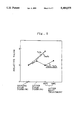
- FIG. 1 is a schematic cross sectional view of a construction of a thin film EL element of a preferred embodiment according to the present invention or a conventional thin film EL element;
- FIG. 2 is a scatter diagram illustrating the relationships between the yttrium amounts in the insulator layers, which included Y 2 O 3 and were employed in the EL elements of the preferred embodiments, and the dielectric breakdown fields exhibited by the insulator layers;
- FIG. 3 is a scatter diagram illustrating the relationships between the tungsten amounts in the insulator layers, which included WO 3 and were employed in the EL elements of the preferred embodiments, and the dielectric breakdown fields exhibited by the insulator layers;
- FIG. 4 is a scatter diagram illustrating the relationships between the yttrium amounts in the insulator layers, which included Y 2 O 3 and were employed in the EL elements of the preferred embodiments, and the relative dielectric constants exhibited by the insulator layers;
- FIG. 5 is a scatter diagram illustrating the relationships between the tungsten amounts in the insulator layers, which included WO 3 and were employed in the EL elements of the preferred embodiments, and the relative dielectric constants exhibited by the insulator layers;
- FIG. 6 is a scatter diagram illustrating the relationships between the yttrium amounts in the insulator layers, which included Y 2 O 3 and were employed in the EL elements of the preferred embodiments, and the figures of merit exhibited by the insulator layers;
- FIG. 7 is a scatter diagram illustrating the relationships between the tungsten amounts in the insulator layers, which included WO 3 and were employed in the EL elements of the preferred embodiments, and the figures of merit exhibited by the insulator layers;
- FIG. 8 is a graph illustrating the relationships between the light-emitting luminances and the applied voltages, relationships which were exhibited by an EL element of a preferred embodiment and an EL element of a comparative example;
- FIG. 9 is a graph illustrating the variations of the electrical resistances exhibited by an indium tin oxide (hereinafter abbreviated to "ITO") film formed on a substrate of an EL element of a preferred embodiment and substrates of EL element of a comparative example; and
- ITO indium tin oxide
- FIG. 10 is a graph illustrating the light-emitting luminance variations against the time passage when an EL element of a preferred embodiment and an EL element of a comparative example were operated continuously.
- FIG. 1 illustrates a schematic cross sectional view of a construction of a thin film EL element of a preferred embodiment according to the present invention.
- the thin film EL element comprises a glass substrate 1, an ITO film formed and stacked on a surface of the glass substrate 1 as a transparent electrode 2, an insulator layer 3 formed and stacked on a surface of the transparent electrode 2, a luminous layer 4 formed and stacked on a surface of the insulator layer 3, an insulator layer 5 formed and stacked on a surface of the luminous layer 4, and an aluminum electrode 6 formed and stacked on a surface of the insulator layer 5 so as to be a topmost surface thereof.
- the insulator layers 3 and 4 are formed of a composite oxide insulator film including Ta 2 O 5 and either Y 2 O 3 or WO 3 .
- the luminous layer 4 is formed of zinc sulfide (ZnS) doped with either terbium (Tb) emitting green light or praseodymium (Pr) emitting white light.
- the insulator layers of the preferred embodiments according to the present invention were examined for their electric characteristics, e.g., dielectric breakdown fields, relative dielectric constants and figures of merit.
- the following six insulator films were formed on Si substrates, and Al was further vacuum-deposited as an electrode on the following six insulator films: a simple Ta 2 O 5 insulator film including Y 2 O 3 in an amount of 0 atomic %, four types of the present composite oxide insulator films including Ta 2 O 5 and Y 2 O 3 in yttrium amounts of 8.2 atomic %, 13.7 atomic %, 19.9 atomic % and 32.0 atomic % with respect to the sum of tantalum and yttrium therein taken as 100 atomic %, and a simple Y 2 O 3 insulator film including Y 2 O 3 in an amount of 100 atomic %.
- the insulator films were formed with a sputtering apparatus, and the sputtering was carried out under the following conditions: each of Y 2 O 3 and Ta 2 O 5 oxide sintered targets was employed.
- the sputtering atmosphere was argon including oxygen in an amount of 30%.
- the Si substrates were kept at a temperature of 300 ° C. during sputtering.
- the insulator films were formed in a thickness of 200 angstroms (i.e., 0.02 micrometers).
- the contents of Y 2 O 3 in the resulting insulator films were analyzed quantitatively by Rutherford Back Scattering analysis.
- FIG. 2 is a scatter diagram which illustrates the relationships between the yttrium amounts of the simple Ta 2 O 5 insulator film free from Y 2 O 3 , the present composite oxide insulator films including Ta 2 O 5 and Y 2 O 3 , and simple the Y 2 O 3 insulator film free from Ta 2 O 5 , and the dielectric breakdown fields E bd thereof.
- the ordinate expresses the dielectric breakdown field E bd (in MV/cm) of the insulator films
- the abscissa expresses the atomic % of yttrium in the insulator films.
- an atomic % of yttrium in an insulator film means the atomic % of yttrium elements in the insulator film when the sum of tantalum elements and yttrium elements therein is taken as 100 atomic %.
- the simple Ta 2 O 5 insulator film including tantalum elements in the amount of 100 atomic % exhibited a dielectric breakdown field in a range of 1.5 to 1.9 MV/cm.
- the present composite oxide insulator films including yttrium in the amount of 8 to 30 atomic % with respect to the sum of tantalum and yttrium therein taken as 100 atomic %, exhibited the dielectric breakdown fields higher than 1.9 MV/cm which is illustrated with a horizontal broken line in FIG. 2 and which was exhibited by the simple Ta 2 O 5 insulator film.
- the dielectric breakdown fields exhibited by the present composite oxide insulator films, including yttrium in the above-described amount with respect to the sum of tantalum and yttrium therein taken as 100 atomic % were approximately twice that of the simple Ta 2 O 5 insulator film.
- FIG. 4 is a scatter diagram which illustrates the relationships between the compositions of the same insulator films (i.e., the simple Ta 2 O 5 insulator film free from Y 2 O 3 , the present composite oxide insulator films including Ta 2 O 5 and Y 2 O 3 , and the simple Y 2 O 3 insulator film free from Ta 2 O 5 ) and the relative dielectric constants " ⁇ r " thereof.
- the ordinate expresses the relative dielectric constant " ⁇ r " of the insulator films
- the abscissa expresses the atomic % of yttrium in the insulator films.
- the relative dielectric constant " ⁇ r " tended to decrease gradually as the yttrium amount increased, but the present composite oxide insulator films including Ta 2 O 5 and Y 2 O 3 exhibited relative dielectric constants " ⁇ r " of approximately at least 16.
- FIG. 6 is a scatter diagram which illustrates the relationships between the compositions of the same insulator films (i.e., the simple Ta 2 O 5 insulator film free from Y 2 O 3 , the present composite oxide insulator films including Ta 2 O 5 and Y 2 O 3 , and the simple Y 2 O 3 insulator film free from Ta 2 O 5 ) and the figures of merit (i.e., the products of the relative dielectric constants and the dielectric breakdown fields) thereof.
- the ordinate expresses the figure of merit
- the abscissa expresses the atomic % of yttrium in the insulator films.
- the present composite oxide insulator films including Ta 2 O 5 and Y 2 O 3 exhibited figures of merit which increased as the yttrium amount increased.
- present composite oxide insulator films including Ta 2 O 5 and Y 2 O 3
- the insulator films thus sandwiched between the Si substrates and the Al electrodes were also evaluated for their dielectric breakdown electric fields, relative dielectric constants and figures of merit. The results of the evaluations were illustrated in FIGS. 3, 5 and 7, respectively.
- FIG. 3 is also a scatter diagram which illustrates the relationships between the tungsten amounts of the simple Ta 2 O 5 insulator film free from WO 3 and the present composite oxide insulator films including Ta 2 O 5 and WO 3 , and the dielectric breakdown fields E bd thereof. Also, in FIG. 3, the ordinate expresses the dielectric breakdown field E bd (in MV/cm) of the insulator films, and the abscissa expresses the atomic % of tungsten in the dielectric films. As can be appreciated from FIG.
- the present composite oxide insulator films including Ta 2 O 5 and WO 3 exhibited dielectric breakdown fields which were improved to approximately twice or more that of the simple Ta 2 O 5 insulator film free from WO 3 .
- the present composite oxide insulator films including Ta 2 O 5 and WO 3 exhibited the dielectric breakdown fields which were deteriorated sharply.
- the present composite oxide insulator film including Ta 2 O 5 and WO 3 exhibited dielectric breakdown fields which were deteriorated below that of the simple Ta 2 O 5 insulator film and which is illustrated with a horizontal broken line in FIG. 3.
- the present composite oxide insulator films of Ta 2 O 5 and WO 3 exhibited higher relative dielectric constants than the simple Ta 2 O 5 insulator film did as illustrated in FIG. 5. Also, in FIG. 5, the ordinate expresses the relative dielectric constant " ⁇ r " of the insulator films, and the abscissa expresses the atomic % of tungsten in the insulator films.
- FIG. 7 which illustrates the figures of merit of the present composite oxide insulator films of Ta 2 O 5 and WO 3
- WO 3 was added into the simple Ta 2 O 5 insulator film in an amount of 2 to 4 atomic % tungsten with respect to the sum of tantalum and tungsten therein taken as 100 atomic %
- the present composite oxide insulator films including Ta 2 O 5 and WO 3 exhibited figures of merit which were twice that of the simple Ta 2 O 5 insulator film free from WO 3 .
- the ordinate expresses the figure of merit
- the abscissa expresses the atomic % of yttrium in the insulator films.
- WO 3 into the simple Ta 2 O 5 insulator film in amount of 2 to 4 atomic % tungsten with respect to the sum of tantalum and tungsten therein taken as 100 atomic %.
- the following five insulator films e.g., the present composite oxide insulator film including Ta 2 O 5 and Y 2 O 3 with yttrium in an amount of 19.9 atomic % with respect to the sum of tantalum and yttrium therein taken as 100 atomic %, the present composite oxide insulator film including Ta 2 O 5 and WO 3 with tungsten in an amount of 3.6 atomic % with respect to the sum of tantalum and tungsten therein taken as 100 atomic %, the simple Ta 2 O 5 insulator film, the simple Y 2 O 3 insulator film, and a simple SiO 2 insulator film, were evaluated for their maximum accumulable electric charges. The results of this evaluation are set forth in Table 1 below together with their dielectric electric breakdown fields and relative dielectric constants.
- the present composite oxide insulator film including Ta 2 O 5 and Y 2 O 3 and the present composite oxide insulator film including Ta 2 O 5 and WO 3 exhibited figures of merit of 84 microcoulomb/cm 2 which were higher than those of the other insulator films.
- the present composite oxide insulator films exhibited remarkably high figures of merit on which the functions of the EL element depend. Therefore, it is very advantageous to add either Y 2 O 3 or WO 3 into the simple Ta 2 O 5 insulator film in order to make a high performance EL element.
- a thin film EL element of a preferred embodiment (hereinafter simply referred to as a "present EL element") was manufactured by using the composite oxide insulator film including Ta 2 O 5 and Y 2 O 3 with an amount of 19.9 atomic % yttrium with respect to the sum of tantalum and yttrium therein taken as 100 atomic %. Namely, as illustrated in FIG.
- an ITO transparent electrode 2 was formed on a glass substrate in a thickness of 0.2 micrometers (i.e., 2000 angstroms), an insulator layer 3 made of the present composite oxide insulator film including Ta 2 O 5 and Y 2 O 3 was formed by sputtering in a thickness of about 0.3 micrometers (i.e., 3000 angstroms).
- Y 2 O 3 and Ta 2 O 5 oxide sintered targets were employed, and the insulator layer 3 was formed with a radio frequency magnetron binary multiple sputtering apparatus.
- wattages applied to the sputtering apparatus were controlled so that a ratio of Y 2 O 3 with respect to the sum of Ta 2 O 5 and Y 2 O 3 is about 20% in an atom-number ratio in the insulator layer 3. Furthermore, since oxygen is insufficiently taken into the insulator layer 3 made of the composite oxide insulator during the formation thereof, oxygen was added into an argon gas in an amount of 30% in order to compensate the oxygen insufficiency. Moreover, the glass substrate 1 was kept at a temperature of 200° C. during the sputtering operation.
- a luminous layer 4 including ZnS doped with Tb emitting green light was formed on the insulator layer 3 in a thickness of about 0.5 micrometers (i.e., 5000 angstroms) in an argon gas atmosphere while keeping the temperature of the glass substrate 1 at 200° C.
- the luminous layer 4 may include ZnS doped with Pr emitting white light.
- an insulator layer 5 was formed on the luminous layer 4 in the same manner as that of insulator layer 3.
- a topmost aluminum electrode 6 was formed on the insulator layer 5 by vacuum-depositing Al in a thickness of about 0.3 micrometers (i.e., 3000 angstroms). The present EL element was thus prepared.
- a comparative EL element was manufactured by forming insulator layers 3' and 5' including Ta 2 O 5 but being free from Y 2 O 3 .
- the comparative EL element had the same construction as that of the present EL element.
- the present EL element includes luminous layer 4 which is a semiconductor containing a compound including at least a combination of a group II element and a group VI element of the Periodic Table.
- the present EL element is a transparent thin film which exhibits a broad band gap, and accordingly it can be regarded as an equivalent circuit, to which a capacitor film is connected in series, provided that a voltage of a light-emitting threshold voltage or less is applied in an electric field required for light-emitting or less.
- the present EL element emits light when a predetermined electric field, e.g., an electric field of 1 to 2 MV/cm, which enables the electrons, emitted from the interface levels between the luminous layer 4 and the insulator layers 3 and 5, to fully excite the luminous centers.
- a predetermined electric field e.g., an electric field of 1 to 2 MV/cm
- the present EL element can be regarded as an equivalent circuit, to which a resistance is connected in parallel.
- the electric field applied to the luminous layer 4 is clamped.
- insulator layers 3 and 5 make the electric current exciting the luminous layer 4 alternately flow stably, thereby regulating the flow direction of the electric current in luminous layer 4.
- insulator layers 3 and 5 stabilize the present EL element.
- the voltage applied to the luminous layer 4 is clamped at a predetermined value. Accordingly, all of the remaining voltage comes to be applied to the insulator layers 3 and 5. Hence, it is necessary to employ a material which exhibits a large dielectric breakdown electric field for the insulator layers 3 and 5.
- the light-emitting luminance of the present EL element depends on the product of the light-emitting efficiency, the number of the luminous centers and the number of the electrons required for the excitation. Let the characteristics of the luminous layer 4 be the same, the light-emitting efficiency is equivalent to the number of the luminous centers, and accordingly the light-emitting luminance of the present EL element depends on the number of the exciting electrons required. Provided that a light-emitting threshold voltage or less is applied in an electric field required for light-emitting or less, the present EL element can be regarded as an equivalent circuit, to which a capacitor film is connected in series.
- the number of the electrons required for the excitation is equivalent to the maximum accumulable electric charges of the insulator layers 3 and 5.
- the present composite oxide insulator films including Ta 2 O 5 and either Y 2 O 3 or WO 3 has superior characteristics to those of other simple insulator films.
- FIG. 8 illustrates light-emitting luminance-applied voltage characteristic curves which were exhibited by the present and the comparative EL elements.
- the present EL element employed insulator layers 3 and 5 made of composite oxide insulator films including Ta 2 O 5 and Y 2 O 3
- the comparative EL element employed the insulator layers 3' and 5' made of the simple Ta 2 O 5 insulator film free from any additive. This is why the present EL element exhibited the threshold value voltages which did not vary as much as the comparative EL element did as illustrated in FIG. 8.
- the present EL element exhibited a higher element-breakdown voltage as well as a higher maximum luminance than the comparative EL elements did, the present EL element could carry out EL light-emission more stably in a wider voltage application range.
- the present EL element could not only exhibit the high luminance and the low threshold voltages, but also operate in a wide operating voltage range satisfactorily.
- the luminous layers 4 of the present and the comparative EL elements were made of material which is likely to absorb moisture in the atmosphere, and accordingly the breakdown of the EL elements often results from the coming-off at the interfaces between the luminous layers 4 and the insulator layers 3 and 5 (or 3' and 5'). Hence, the lives and the stabilities of the EL elements are believed to depend on the adhesion between the luminous layer 4 and the insulator layers 3 and 5 (or 3' and 5'). If the breakdown of one pixel does not result in the breakdown of other pixels, the reliabilities and the lives of the entire EL element can be upgraded.
- the film forming processes and the film forming conditions vary the adhesion between the luminous layer 4 and the insulator layers 3 and 5, it is believed that the adhesion depends on portions of the luminous layer 4 and the insulator layers 3 and 5 in which the atoms are bonded chemically. Therefore, it is necessary to employ a material which exhibits good adhesion to the luminous layer 4 for the insulator layers 3 and 5.
- Table 2 below sets forth the evaluation results on the adhesion between the luminous layer 4 and the insulator layers 3 and 5 of the present EL element and those of the comparative EL elements.
- the evaluation was carried out by subjecting the EL elements to a so-called peeling test.
- a Scotch tape (registered trade mark) was first applied on the insulator layer 5 or 5'. Then, the tape was peeled off, and the insulator layers 5 or 5' was examined to determine whether it remained on the luminous layer 4 or not.
- the insulator layer 5' was made of the simple Ta 2 O 5 insulator film, the insulator layer 5' came off with tape easily.
- the insulator layer 5 of the present EL element was made by adding Y 2 O 3 , which inherently exhibits a good adhesion and a strong electronic affinity to the luminous layer 4, into the simple Ta 2 O 5 insulator film.
- the bonding was improved at the interface between the luminous layer 4 the insulator layer 5 of the present EL element by the yttrium atoms. It goes without saying that the same evaluation results could have been obtained if the insulator layers 3 and 3' were tested similarly.
- the comparative EL elements i.e., conventional EL elements, exhibited breakdown modes of the propagation type during breakdown.
- the present EL element basically exhibited the breakdown mode of the self-healing type during breakdown.
- the breakdown mode depends on the state of the interface between the ITO transparent electrode 2 and the insulator layer 3, the state of the interface between the aluminum electrode 6 and the insulator layer 5, or the states of the interfaces between the luminous layer 4 and the insulator layers 3 and 5.
- the breakdown mode also depends on insulator materials.
- the mechanism of the breakdown has not been explained explicitly yet; however, roughly speaking, it is believed to occur as follows: the microstructural defects in insulator layers 3 and 5, the vacant oxygen lattices therein and the vacant metal lattices therein trap electrons, and the trapped electrons form passages for electric currents, and breakdown eventually occurs. In the meantime, the electric currents generate Joule heat. As a result, the insulator layers 3 and 5 or the electrodes 2 and 6 evaporate locally, they discharge electrically, and thereby mechanical fractures occur. Thus, it is believed that the breakdown mode depends on the vapor pressures of the insulator materials, the thermal expansion coefficient differences resulting from the heat generation, etc.
- the present EL element not only the electrical properties of the simple Ta 2 O 5 insulator film, but also the thermal and the mechanical properties thereof were improved by adding Y 2 O 3 into the simple Ta 2 O 5 insulator film.
- the Y 2 O 3 addition transformed one of the conventional characteristics of the simple Ta 2 O 5 insulator film, e.g., the propagation type breakdown mode, into the self-healing type breakdown mode in the present EL element.
- the resistance value of the ITO transparent electrode 2 is increased by the following mechanisms: when an oxide insulator layer adjacent to the ITO transparent electrode 2 is instable, the indium (In) of the ITO transparent electrode 2 diffuses into the oxide insulator layer so that the resistance value of the ITO transparent electrode 2 is increased, or the resistance value of the ITO transparent electrode 2 is increased by the oxidation or the reduction reaction of the ITO transparent electrode 2.
- FIG. 9 illustrates the resistance value variations of ITO transparent electrodes 2 during the production processes of the present and the comparative EL elements.
- the present EL element hardly exhibited resistance value variation when compared with those exhibited by the comparative EL elements. It is believed that there arose stable composite oxides by adding Y 2 O 3 into Ta 2 O 5 , and that the stable composite oxides hardly reacted with the ITO transparent electrode 2 even when the present EL element was subjected to heat treatments.
- the present EL element includes the insulator layers 3 and 5 which are made of the composite oxide insulator films, and accordingly the insulator film formation process can be simplified in the production process of the present EL element.
- the present EL element includes insulator layers 3 and 5 which are made of composite oxide insulator film including Ta 2 O 5 and Y 2 O 3 , and accordingly it provides the following advantageous effects: it is improved in terms of adhesion, it is made to exhibit the self-healing type breakdown mode, and it includes the ITO transparent electrode 2 whose resistance value is hardly increased. As a result, the present EL element can be operated stably even when it is operated for a long period of time.
- FIG. 10 illustrates the light-emitting variations of the present and the comparative EL elements with respect to the time passage.
- the present and comparative EL elements were made to include a luminous layer 4 which contained Pr as the luminous centers, they were enclosed merely with an epoxy resin, and they were operated for a long period of time in the atmosphere.
- the present thin film EL element was confirmed to operate stably for a period of 2000 hours or more, and accordingly it was superior in reliability. This advantageous effect results from the fact that the predetermined voltage was applied to the luminous layer 4 so stably that the insulator layers 3 and 5 holding the luminous layer 4 therebetween were improved in terms of stability.
- one of the initial characteristics of the present EL element e.g., the light-emitting luminance-applied voltage characteristic illustrated in FIG. 8, depends on the maximum accumulable electric charges of the insulator layers 3 and 5. As can be seen from FIG. 8, the initial characteristic of the present EL element was stabilized, and its life was prolonged. This advantageous effect resulted from the construction of the present EL element.
- the present EL element included insulator layers 3 and 5 which satisfied the following key factors for making the present EL element stable and long lived: the adhesion between the insulator layer 3 or 5 and luminous layer 4 as well as the adhesion between the insulator layer 3 or 4 and the ITO transparent electrode 2 or the aluminum electrode 6 was improved, the overall construction was made to exhibit a self-healing type breakdown mode, and the ITO transparent electrode 2 was made to exhibit a resistance value which hardly varied.
- the comparative EL element underwent breakdown approximately 1000 hours earlier as illustrated in FIG. 10, and it had a short period of life.
- the following are believed to be the causes of the short life: the adhesion was inferior to those described above, the overall construction exhibited the propagation type breakdown mode, etc.
- the comparative EL element suffered from factors which adversely affected the reliability and the stability.
Abstract
Description
              TABLE 1
______________________________________
           Figure of               Dielectric
           Merit        Relative   Breakdown
           (microcoulomb
                        Dielectric Field
Composition
           /cm.sup.2)   Constant   (MV/cm)
______________________________________
Ta.sub.2 O.sub.5 + Y.sub.2 O.sub.3
           84           21         4
Ta.sub.2 O.sub.5 + WO.sub.3
           84           21         4
Ta.sub.2 O.sub.5
           84           23         2
Y.sub.2 O.sub.3
           12           12         1
SiO.sub.2  32            4         8
______________________________________
 Note: Thicknesses of the insulator films were 0.08 micrometers (i.e., 800
 angstroms).
V.sub.i =V.sub.tot /{1+(C.sub.z /C.sub.i)}.
              TABLE 2
______________________________________
Composition     Adhesion
______________________________________
Ta.sub.2 O.sub.5 + Y.sub.2 O.sub.3
                Good
Ta.sub.2 O.sub.5
                Bad
Y.sub.2 O.sub.3 Good
______________________________________
              TABLE 3
______________________________________
Composition        Breakdown Mode
______________________________________
Ta.sub.2 O.sub.5 + Y.sub.2 O.sub.3
                   Self-healing Type
Ta.sub.2 O.sub.5   Propagation Type
Y.sub.2 O.sub.3    Self-healing Type
SiO.sub.2          Self-healing Type
______________________________________
Claims (8)
Applications Claiming Priority (2)
| Application Number | Priority Date | Filing Date | Title |
|---|---|---|---|
| JP3344758A JPH05182766A (en) | 1991-12-26 | 1991-12-26 | Thin film el element |
| JP3-344758 | 1991-12-26 |
Publications (1)
| Publication Number | Publication Date |
|---|---|
| US5404075A true US5404075A (en) | 1995-04-04 |
Family
ID=18371751
Family Applications (1)
| Application Number | Title | Priority Date | Filing Date |
|---|---|---|---|
| US07/964,965 Expired - Fee Related US5404075A (en) | 1991-12-26 | 1992-10-22 | TFEL element with tantalum oxide and tungsten oxide insulating layer |
Country Status (2)
| Country | Link |
|---|---|
| US (1) | US5404075A (en) |
| JP (1) | JPH05182766A (en) |
Cited By (19)
| Publication number | Priority date | Publication date | Assignee | Title |
|---|---|---|---|---|
| US5589733A (en) * | 1994-02-17 | 1996-12-31 | Kabushiki Kaisha Toyota Chuo Kenkyusho | Electroluminescent element including a dielectric film of tantalum oxide and an oxide of either indium, tin, or zinc |
| US5789860A (en) * | 1995-08-11 | 1998-08-04 | Nippondenso Co., Ltd. | Dielectric thin film composition and thin-film EL device using same |
| US20030134149A1 (en) * | 2002-01-16 | 2003-07-17 | Mitsui Chemicals, Inc. | Transparent conductive film and electroluminescence light emitting device therewith |
| US20040211971A1 (en) * | 2002-05-14 | 2004-10-28 | Manabu Takei | Luminescent panel |
| US20050072977A1 (en) * | 2003-10-03 | 2005-04-07 | Semiconductor Energy Laboratory Co., Ltd. | Light emitting element and manufacturing method thereof, and light emitting device using the light emitting element |
| US20060232203A1 (en) * | 2005-03-25 | 2006-10-19 | Semiconductor Energy Laboratory Co., Ltd. | Light emitting device |
| US20060263638A1 (en) * | 2005-05-20 | 2006-11-23 | Semiconductor Energy Laboratory Co., Ltd. | Light emitting element, light emitting device, and electronic device |
| US20060284189A1 (en) * | 2005-06-08 | 2006-12-21 | Junichiro Sakata | Light-emitting element, light-emitting device, and electronic device |
| US20070013301A1 (en) * | 2005-06-30 | 2007-01-18 | Shunpei Yamazaki | Light emitting element, light emitting device, and electronic apparatus |
| US20070114527A1 (en) * | 2003-12-26 | 2007-05-24 | Semiconductor Energy Laboratory Co., Ltd. | Light-emitting element |
| US20070114544A1 (en) * | 2004-09-24 | 2007-05-24 | Semiconductor Energy Laboratory Co., Ltd. | Light emitting device |
| US20070200125A1 (en) * | 2003-09-26 | 2007-08-30 | Hisao Ikeda | Light-Emitting Device And Method For Manufacturing The Same |
| US20070262693A1 (en) * | 2004-10-29 | 2007-11-15 | Satoshi Seo | Composite Material, Light-Emitting Element, Light-Emitting Device and Manufacturing Method Thereof |
| US20080191611A1 (en) * | 2005-03-23 | 2008-08-14 | Semiconductor Energy Laboratory Co., Ltd. | Composite Material, Light Emitting Element and Light Emitting Device |
| US20100123152A1 (en) * | 2008-11-19 | 2010-05-20 | Semiconductor Energy Laboratory Co., Ltd. | Light-Emitting Element, Light-Emitting Device, Electronic Device, and Lighting Device |
| US7893427B2 (en) | 2004-07-23 | 2011-02-22 | Semiconductor Energy Laboratory Co., Ltd. | Light emitting element and light emitting device using the same |
| US20110101379A1 (en) * | 2009-11-02 | 2011-05-05 | Semiconductor Energy Laboratory Co., Ltd. | Method for Manufacturing Light-Emitting Element, Light-Emitting Element, Light-Emitting Device, Lighting Device, and Electronic Appliance |
| US8896014B2 (en) | 2010-11-24 | 2014-11-25 | Semiconductor Energy Laboratory Co., Ltd. | Light-emitting element, manufacturing method thereof, and lighting device |
| US9564609B2 (en) | 2011-02-11 | 2017-02-07 | Semiconductor Energy Laboratory Co., Ltd. | Light-emitting element including electrode of three layers |
Citations (12)
| Publication number | Priority date | Publication date | Assignee | Title |
|---|---|---|---|---|
| JPS5027488A (en) * | 1973-07-10 | 1975-03-20 | ||
| US4054531A (en) * | 1974-11-07 | 1977-10-18 | Tdk Electronics Co., Ltd. | Ceramic dielectric composition |
| US4392907A (en) * | 1979-03-27 | 1983-07-12 | Canon Kabushiki Kaisha | Method for producing recording head |
| JPS58216391A (en) * | 1982-06-10 | 1983-12-16 | 株式会社リコー | Thin film el element |
| US4670355A (en) * | 1984-02-29 | 1987-06-02 | Hoya Corporation | Electroluminescent panel comprising a dielectric layer of a mixture of tantalum oxide and aluminum oxide |
| US4727004A (en) * | 1985-11-21 | 1988-02-23 | Sharp Kabushiki Kaisha | Thin film electroluminescent device |
| US4733128A (en) * | 1983-02-10 | 1988-03-22 | Matsushita Electric Industrial Co. Ltd. | Electroluminescence display device containing a zinc sulfide emission layer with rare earth elements and/or halides thereof and phosphorus |
| JPS6454692A (en) * | 1987-08-25 | 1989-03-02 | Kansai Nippon Electric | Thin film el element |
| US5037709A (en) * | 1988-07-21 | 1991-08-06 | Sharp Kabushiki Kaisha | Electroluminescent device of compound semiconductor |
| US5099172A (en) * | 1987-11-09 | 1992-03-24 | Hitachi, Ltd. | Thin film electroluminescent device |
| US5161233A (en) * | 1988-05-17 | 1992-11-03 | Dai Nippon Printing Co., Ltd. | Method for recording and reproducing information, apparatus therefor and recording medium |
| US5225286A (en) * | 1991-06-13 | 1993-07-06 | Kabushiki Kaisha Toyota Chuo Kenkyusho | Dielectric film |
-
1991
- 1991-12-26 JP JP3344758A patent/JPH05182766A/en active Pending
-
1992
- 1992-10-22 US US07/964,965 patent/US5404075A/en not_active Expired - Fee Related
Patent Citations (12)
| Publication number | Priority date | Publication date | Assignee | Title |
|---|---|---|---|---|
| JPS5027488A (en) * | 1973-07-10 | 1975-03-20 | ||
| US4054531A (en) * | 1974-11-07 | 1977-10-18 | Tdk Electronics Co., Ltd. | Ceramic dielectric composition |
| US4392907A (en) * | 1979-03-27 | 1983-07-12 | Canon Kabushiki Kaisha | Method for producing recording head |
| JPS58216391A (en) * | 1982-06-10 | 1983-12-16 | 株式会社リコー | Thin film el element |
| US4733128A (en) * | 1983-02-10 | 1988-03-22 | Matsushita Electric Industrial Co. Ltd. | Electroluminescence display device containing a zinc sulfide emission layer with rare earth elements and/or halides thereof and phosphorus |
| US4670355A (en) * | 1984-02-29 | 1987-06-02 | Hoya Corporation | Electroluminescent panel comprising a dielectric layer of a mixture of tantalum oxide and aluminum oxide |
| US4727004A (en) * | 1985-11-21 | 1988-02-23 | Sharp Kabushiki Kaisha | Thin film electroluminescent device |
| JPS6454692A (en) * | 1987-08-25 | 1989-03-02 | Kansai Nippon Electric | Thin film el element |
| US5099172A (en) * | 1987-11-09 | 1992-03-24 | Hitachi, Ltd. | Thin film electroluminescent device |
| US5161233A (en) * | 1988-05-17 | 1992-11-03 | Dai Nippon Printing Co., Ltd. | Method for recording and reproducing information, apparatus therefor and recording medium |
| US5037709A (en) * | 1988-07-21 | 1991-08-06 | Sharp Kabushiki Kaisha | Electroluminescent device of compound semiconductor |
| US5225286A (en) * | 1991-06-13 | 1993-07-06 | Kabushiki Kaisha Toyota Chuo Kenkyusho | Dielectric film |
Cited By (69)
| Publication number | Priority date | Publication date | Assignee | Title |
|---|---|---|---|---|
| US5589733A (en) * | 1994-02-17 | 1996-12-31 | Kabushiki Kaisha Toyota Chuo Kenkyusho | Electroluminescent element including a dielectric film of tantalum oxide and an oxide of either indium, tin, or zinc |
| US5789860A (en) * | 1995-08-11 | 1998-08-04 | Nippondenso Co., Ltd. | Dielectric thin film composition and thin-film EL device using same |
| US6036823A (en) * | 1995-08-11 | 2000-03-14 | Denso Corporation | Dielectric thin film and thin-film EL device using same |
| US20030134149A1 (en) * | 2002-01-16 | 2003-07-17 | Mitsui Chemicals, Inc. | Transparent conductive film and electroluminescence light emitting device therewith |
| US20040211971A1 (en) * | 2002-05-14 | 2004-10-28 | Manabu Takei | Luminescent panel |
| US7511419B2 (en) * | 2002-05-14 | 2009-03-31 | Casio Computer Co., Ltd. | Luminescent panel having a reflecting film to reflect light outwardly which is shaped to condense the reflected light |
| US8507903B2 (en) | 2003-09-26 | 2013-08-13 | Semiconductor Energy Laboratory Co., Ltd. | Light-emitting device and method for manufacturing the same |
| US7732808B2 (en) | 2003-09-26 | 2010-06-08 | Semiconductor Energy Laboratory Co., Ltd | Light-emitting device and method for manufacturing the same |
| US8216875B2 (en) | 2003-09-26 | 2012-07-10 | Semiconductor Energy Laboratory Co., Ltd. | Light-emitting device and method for manufacturing the same |
| US8178869B2 (en) | 2003-09-26 | 2012-05-15 | Semiconductor Energy Laboratory Co., Ltd. | Light-emitting device and method for manufacturing the same |
| US20070200125A1 (en) * | 2003-09-26 | 2007-08-30 | Hisao Ikeda | Light-Emitting Device And Method For Manufacturing The Same |
| US20100207518A1 (en) * | 2003-09-26 | 2010-08-19 | Semiconductor Energy Laboratory Co., Ltd. | Light-emitting device and method for manufacturing the same |
| US8994007B2 (en) | 2003-10-03 | 2015-03-31 | Semiconductor Energy Laboratory Co., Ltd. | Light emitting element and manufacturing method thereof, and light emitting device using the light emitting element |
| US7994496B2 (en) | 2003-10-03 | 2011-08-09 | Semiconductor Energy Laboratory Co., Ltd. | Light emitting element and manufacturing method thereof, and light emitting device using the light emitting element |
| US9461271B2 (en) | 2003-10-03 | 2016-10-04 | Semiconductor Energy Laboratory Co., Ltd. | Light emitting element and manufacturing method thereof, and light emitting device using the light emitting element |
| US7387904B2 (en) | 2003-10-03 | 2008-06-17 | Semiconductor Energy Laboratory Co., Ltd. | Light emitting element and manufacturing method thereof, and light emitting device using the light emitting element |
| US20080203385A1 (en) * | 2003-10-03 | 2008-08-28 | Semiconductor Energy Laboratory Co., Ltd. | Light emitting element and manufacturing method thereof, and light emitting device using the light emitting element |
| US20050072977A1 (en) * | 2003-10-03 | 2005-04-07 | Semiconductor Energy Laboratory Co., Ltd. | Light emitting element and manufacturing method thereof, and light emitting device using the light emitting element |
| US20110156030A1 (en) * | 2003-12-26 | 2011-06-30 | Semiconductor Energy Laboratory Co., Ltd. | Light-emitting element |
| US9570697B2 (en) | 2003-12-26 | 2017-02-14 | Semiconductor Energy Laboratory Co., Ltd. | Light-emitting element |
| US10886497B2 (en) | 2003-12-26 | 2021-01-05 | Semiconductor Energy Laboratory Co., Ltd. | Light-emitting element |
| US8796670B2 (en) | 2003-12-26 | 2014-08-05 | Semiconductor Energy Laboratory Co., Ltd. | Light-emitting element |
| US20070114527A1 (en) * | 2003-12-26 | 2007-05-24 | Semiconductor Energy Laboratory Co., Ltd. | Light-emitting element |
| US7893427B2 (en) | 2004-07-23 | 2011-02-22 | Semiconductor Energy Laboratory Co., Ltd. | Light emitting element and light emitting device using the same |
| US8368060B2 (en) | 2004-07-23 | 2013-02-05 | Semiconductor Energy Laboratory Co., Ltd. | Light emitting element and light emitting device using the same |
| US8368059B2 (en) | 2004-07-23 | 2013-02-05 | Semiconductor Energy Laboratory Co., Ltd. | Light emitting element and light emitting device using the same |
| US8872169B2 (en) | 2004-07-23 | 2014-10-28 | Semiconductor Energy Laboratory Co., Ltd. | Light emitting element and light emitting device using the same |
| US9520532B2 (en) | 2004-07-23 | 2016-12-13 | Semiconductor Energy Laboratory Co., Ltd. | Light emitting element and light emitting device using the same |
| US20110101345A1 (en) * | 2004-07-23 | 2011-05-05 | Semiconductor Energy Laboratory Co., Ltd. | Light emitting element and light emitting device using the same |
| US20110101380A1 (en) * | 2004-07-23 | 2011-05-05 | Semiconductor Energy Laboratory Co., Ltd. | Light emitting element and light emitting device using the same |
| US8643003B2 (en) | 2004-09-24 | 2014-02-04 | Semiconductor Energy Laboratory Co., Ltd. | Light emitting device |
| US20070114544A1 (en) * | 2004-09-24 | 2007-05-24 | Semiconductor Energy Laboratory Co., Ltd. | Light emitting device |
| US8008652B2 (en) | 2004-09-24 | 2011-08-30 | Semiconductor Energy Laboratory Co., Ltd. | Light emitting device |
| US10134996B2 (en) | 2004-10-29 | 2018-11-20 | Semicondcutor Energy Laboratory Co., Ltd. | Composite material, light-emitting element, light-emitting device, and manufacturing method thereof |
| US20070262693A1 (en) * | 2004-10-29 | 2007-11-15 | Satoshi Seo | Composite Material, Light-Emitting Element, Light-Emitting Device and Manufacturing Method Thereof |
| US20080191611A1 (en) * | 2005-03-23 | 2008-08-14 | Semiconductor Energy Laboratory Co., Ltd. | Composite Material, Light Emitting Element and Light Emitting Device |
| US8420227B2 (en) | 2005-03-23 | 2013-04-16 | Semiconductor Energy Laboratory Co., Ltd. | Composite material, light emitting element and light emitting device |
| US8916276B2 (en) | 2005-03-23 | 2014-12-23 | Semiconductor Energy Laboratory Co., Ltd. | Composite material, light emitting element and light emitting device |
| US8362688B2 (en) | 2005-03-25 | 2013-01-29 | Semiconductor Energy Laboratory Co., Ltd. | Light emitting device |
| US9246056B2 (en) | 2005-03-25 | 2016-01-26 | Semiconductor Energy Laboratory Co., Ltd. | Light emitting device |
| US7851989B2 (en) | 2005-03-25 | 2010-12-14 | Semiconductor Energy Laboratory Co., Ltd. | Light emitting device |
| US20110140101A1 (en) * | 2005-03-25 | 2011-06-16 | Semiconductor Energy Laboratory Co., Ltd. | Light Emitting Device |
| US20060232203A1 (en) * | 2005-03-25 | 2006-10-19 | Semiconductor Energy Laboratory Co., Ltd. | Light emitting device |
| US20100308320A1 (en) * | 2005-05-20 | 2010-12-09 | Semiconductor Energy Laboratory Co., Ltd. | Light emitting element, light emitting device, and electronic device |
| US8227097B2 (en) | 2005-05-20 | 2012-07-24 | Semiconductor Energy Laboratory Co., Ltd. | Light emitting element, light emitting device, and electronic device |
| US8048543B2 (en) | 2005-05-20 | 2011-11-01 | Semiconductor Energy Laboratory Co., Ltd. | Light emitting element, light emitting device, and electronic device |
| US7883788B2 (en) | 2005-05-20 | 2011-02-08 | Semiconductor Energy Laboratory Co., Ltd. | Light emitting element, light emitting device, and electronic device |
| US8445121B2 (en) | 2005-05-20 | 2013-05-21 | Semiconductor Energy Laboratory Co., Ltd. | Light emitting element, light emitting device, and electronic device |
| US20060263638A1 (en) * | 2005-05-20 | 2006-11-23 | Semiconductor Energy Laboratory Co., Ltd. | Light emitting element, light emitting device, and electronic device |
| US7790296B2 (en) | 2005-05-20 | 2010-09-07 | Semiconductor Energy Laboratory Co., Ltd. | Light emitting element, light emitting device, and electronic device |
| US20110108828A1 (en) * | 2005-05-20 | 2011-05-12 | Semiconductor Energy Laboratory Co., Ltd. | Light emitting element, light emitting device, and electronic device |
| US8334057B2 (en) | 2005-06-08 | 2012-12-18 | Semiconductor Energy Laboratory Co., Ltd. | Light-emitting element, light-emitting device, and electronic device |
| US9263645B2 (en) | 2005-06-08 | 2016-02-16 | Semiconductor Energy Laboratory Co., Ltd. | Light-emitting element, light-emitting device, and electronic device |
| US20060284189A1 (en) * | 2005-06-08 | 2006-12-21 | Junichiro Sakata | Light-emitting element, light-emitting device, and electronic device |
| US8378570B2 (en) | 2005-06-30 | 2013-02-19 | Semiconductor Energy Laboratory Co., Ltd. | Light emitting element, light emitting device, and electronic apparatus having first and second composite layers with different metal concentrations |
| US7948169B2 (en) | 2005-06-30 | 2011-05-24 | Semiconductor Energy Larboratory Co., Ltd. | Light emitting element with composite layers of varying concentration, light emitting device, and electronic apparatus |
| US7745989B2 (en) | 2005-06-30 | 2010-06-29 | Semiconductor Energy Laboratory Co., Ltd | Light emitting element, light emitting device, and electronic apparatus |
| US20070013301A1 (en) * | 2005-06-30 | 2007-01-18 | Shunpei Yamazaki | Light emitting element, light emitting device, and electronic apparatus |
| KR101356095B1 (en) * | 2005-06-30 | 2014-01-28 | 가부시키가이샤 한도오따이 에네루기 켄큐쇼 | Light emitting element, light emitting device, and electronic apparatus |
| US8519617B2 (en) | 2005-06-30 | 2013-08-27 | Semiconductor Energy Laboratory Co., Ltd. | Light emitting element having a metal oxide composite layer, and light emitting device, and electronic apparatus |
| US20100258792A1 (en) * | 2005-06-30 | 2010-10-14 | Semiconductor Energy Laboratory Co., Ltd. | Light emitting element, light emitting device, and electronic apparatus |
| US20110198585A1 (en) * | 2005-06-30 | 2011-08-18 | Semiconductor Energy Laboratory Co., Ltd. | Light emitting element, light emitting device, and electronic apparatus |
| US20100123152A1 (en) * | 2008-11-19 | 2010-05-20 | Semiconductor Energy Laboratory Co., Ltd. | Light-Emitting Element, Light-Emitting Device, Electronic Device, and Lighting Device |
| US9224976B2 (en) | 2008-11-19 | 2015-12-29 | Semiconductor Energy Laboratory Co., Ltd. | Light-emitting element, light-emitting device, electronic device, and lighting device |
| US8404500B2 (en) | 2009-11-02 | 2013-03-26 | Semiconductor Energy Laboratory Co., Ltd. | Method for manufacturing light-emitting element, light-emitting element, light-emitting device, lighting device, and electronic appliance |
| US8803188B2 (en) | 2009-11-02 | 2014-08-12 | Semiconductor Energy Laboratory Co., Ltd. | Method for manufacturing light-emitting element, light-emitting element, Light-emitting device, lighting device, and electronic appliance |
| US20110101379A1 (en) * | 2009-11-02 | 2011-05-05 | Semiconductor Energy Laboratory Co., Ltd. | Method for Manufacturing Light-Emitting Element, Light-Emitting Element, Light-Emitting Device, Lighting Device, and Electronic Appliance |
| US8896014B2 (en) | 2010-11-24 | 2014-11-25 | Semiconductor Energy Laboratory Co., Ltd. | Light-emitting element, manufacturing method thereof, and lighting device |
| US9564609B2 (en) | 2011-02-11 | 2017-02-07 | Semiconductor Energy Laboratory Co., Ltd. | Light-emitting element including electrode of three layers |
Also Published As
| Publication number | Publication date |
|---|---|
| JPH05182766A (en) | 1993-07-23 |
Similar Documents
| Publication | Publication Date | Title |
|---|---|---|
| US5404075A (en) | TFEL element with tantalum oxide and tungsten oxide insulating layer | |
| US6005342A (en) | Luminescent device having phosphor particles about .5 micrometers or less and plasma discharge chamber for generating U.V. light | |
| US5072263A (en) | Thin film el device with protective film | |
| US5589733A (en) | Electroluminescent element including a dielectric film of tantalum oxide and an oxide of either indium, tin, or zinc | |
| US4486499A (en) | Electroluminescent device | |
| JPS5823191A (en) | Thin film el element | |
| US4464602A (en) | Thin film electroluminescent device | |
| US4947081A (en) | Dual insulation oxynitride blocking thin film electroluminescence display device | |
| US20050140271A1 (en) | Electroluminescent cell and electroluminescent particle | |
| US4777099A (en) | Thin-film EL device | |
| KR100317989B1 (en) | High luminance blue dc-electroluminescent display | |
| EP0163351B1 (en) | Thin film electroluminescent device | |
| JP2000113983A (en) | Display device | |
| JPS6323640B2 (en) | ||
| KR970006081B1 (en) | Manufacturing method of thin-film el display element | |
| JPH027072B2 (en) | ||
| JPS6124192A (en) | Thin film electroluminescent element | |
| JPS5855636B2 (en) | Thin film EL element | |
| JPS5820468B2 (en) | Blackened electrode structure | |
| JPS598040B2 (en) | Thin film EL element | |
| JPS59154794A (en) | Thin film el element | |
| JPH07192871A (en) | Thin film el element | |
| JPS5855635B2 (en) | Thin film EL element | |
| JP2001176671A (en) | Electroluminescent element and its manufacturing method | |
| KR20000013291A (en) | El phenomena-applied identification sensor |
Legal Events
| Date | Code | Title | Description |
|---|---|---|---|
| AS | Assignment |
Owner name: KABUSHIKI KAISHA TOYOTA CHUO KENKYUSHO, JAPAN Free format text: ASSIGNMENT OF ASSIGNORS INTEREST.;ASSIGNORS:FUJIKAWA, HISAYOSHI;TAGA, YASUNORI;REEL/FRAME:006387/0651 Effective date: 19920818 |
|
| AS | Assignment |
Owner name: NIPPONDENSO CO., LTD., JAPAN Free format text: ASSIGNMENT OF ASSIGNORS INTEREST;ASSIGNOR:KABUSHIKI KAISHA TOYOTA CHUO KENKYUSHO;REEL/FRAME:006934/0187 Effective date: 19940314 |
|
| AS | Assignment |
Owner name: NIPPONDENSO CO., LTD. (1/2 INTEREST) Free format text: CORRECTED RECORDATION FORM COVER SHEET, REEL/FRAME 6934/187-189.;ASSIGNOR:KABUSHKI KAISHA TOYOTA CHUO KENKYUSHO;REEL/FRAME:007402/0654 Effective date: 19940314 |
|
| FPAY | Fee payment |
Year of fee payment: 4 |
|
| AS | Assignment |
Owner name: DENSO CORPORATION, JAPAN Free format text: CHANGE OF NAME;ASSIGNOR:NIPPONDENSCO CO., LTD.;REEL/FRAME:012153/0333 Effective date: 19961001 Owner name: DENSO CORPORATION, JAPAN Free format text: ASSIGNMENT OF ASSIGNORS INTEREST;ASSIGNOR:KABUSHIKI KAISHA TOYOTA CHUO KENKYUSHO;REEL/FRAME:012153/0393 Effective date: 20010730 |
|
| FPAY | Fee payment |
Year of fee payment: 8 |
|
| FEPP | Fee payment procedure |
Free format text: PAYER NUMBER DE-ASSIGNED (ORIGINAL EVENT CODE: RMPN); ENTITY STATUS OF PATENT OWNER: LARGE ENTITY Free format text: PAYOR NUMBER ASSIGNED (ORIGINAL EVENT CODE: ASPN); ENTITY STATUS OF PATENT OWNER: LARGE ENTITY |
|
| REMI | Maintenance fee reminder mailed | ||
| LAPS | Lapse for failure to pay maintenance fees | ||
| STCH | Information on status: patent discontinuation |
Free format text: PATENT EXPIRED DUE TO NONPAYMENT OF MAINTENANCE FEES UNDER 37 CFR 1.362 |
|
| FP | Lapsed due to failure to pay maintenance fee |
Effective date: 20070404 |