US5373245A - Capaciflector camera - Google Patents
Capaciflector camera Download PDFInfo
- Publication number
- US5373245A US5373245A US08/090,230 US9023093A US5373245A US 5373245 A US5373245 A US 5373245A US 9023093 A US9023093 A US 9023093A US 5373245 A US5373245 A US 5373245A
- Authority
- US
- United States
- Prior art keywords
- sensor
- conductors
- shield
- insulation
- current
- Prior art date
- Legal status (The legal status is an assumption and is not a legal conclusion. Google has not performed a legal analysis and makes no representation as to the accuracy of the status listed.)
- Expired - Lifetime
Links
Images


Classifications
-
- H—ELECTRICITY
- H03—ELECTRONIC CIRCUITRY
- H03K—PULSE TECHNIQUE
- H03K17/00—Electronic switching or gating, i.e. not by contact-making and –breaking
- H03K17/94—Electronic switching or gating, i.e. not by contact-making and –breaking characterised by the way in which the control signals are generated
- H03K17/945—Proximity switches
- H03K17/955—Proximity switches using a capacitive detector
-
- G—PHYSICS
- G01—MEASURING; TESTING
- G01V—GEOPHYSICS; GRAVITATIONAL MEASUREMENTS; DETECTING MASSES OR OBJECTS; TAGS
- G01V3/00—Electric or magnetic prospecting or detecting; Measuring magnetic field characteristics of the earth, e.g. declination, deviation
- G01V3/08—Electric or magnetic prospecting or detecting; Measuring magnetic field characteristics of the earth, e.g. declination, deviation operating with magnetic or electric fields produced or modified by objects or geological structures or by detecting devices
- G01V3/088—Electric or magnetic prospecting or detecting; Measuring magnetic field characteristics of the earth, e.g. declination, deviation operating with magnetic or electric fields produced or modified by objects or geological structures or by detecting devices operating with electric fields
-
- H—ELECTRICITY
- H03—ELECTRONIC CIRCUITRY
- H03K—PULSE TECHNIQUE
- H03K2217/00—Indexing scheme related to electronic switching or gating, i.e. not by contact-making or -breaking covered by H03K17/00
- H03K2217/94—Indexing scheme related to electronic switching or gating, i.e. not by contact-making or -breaking covered by H03K17/00 characterised by the way in which the control signal is generated
- H03K2217/96—Touch switches
- H03K2217/9607—Capacitive touch switches
- H03K2217/960735—Capacitive touch switches characterised by circuit details
- H03K2217/96075—Capacitive touch switches characterised by circuit details involving bridge circuit
-
- H—ELECTRICITY
- H03—ELECTRONIC CIRCUITRY
- H03K—PULSE TECHNIQUE
- H03K2217/00—Indexing scheme related to electronic switching or gating, i.e. not by contact-making or -breaking covered by H03K17/00
- H03K2217/94—Indexing scheme related to electronic switching or gating, i.e. not by contact-making or -breaking covered by H03K17/00 characterised by the way in which the control signal is generated
- H03K2217/96—Touch switches
- H03K2217/9607—Capacitive touch switches
- H03K2217/960755—Constructional details of capacitive touch and proximity switches
- H03K2217/960765—Details of shielding arrangements
Definitions
- This invention relates to capacitive proximity sensors and more particularly to a capacitive sensor that will permit 3-D imaging by electrically scanning rows and columns useful for collision avoidance situations.
- Capacitive-Controlled Oscillator (CCO) based "capaciflector” proximity sensors and CCO based sensor arrays are available (see FIG. 1a and U.S. Pat. No. 5,166,679 for a discussion of the basic "capaciflector” technology).
- CCO based "capaciflector” sensors can be used as arrays only where the separation between individual sensors can be made large, such as 3 to 6 inches.
- the shield must be much larger that the sensor (on the order of 7 times wider) and each sensor must have its own shield. The shield is slaved to the sensor via a voltage follower, so it changes frequency with the sensor. If another sensor is introduced, another CCO and voltage follower shield must be added.
- the sensors must be spaced no closer than the width of the shields. Even then, there is some cross talk because the two sensors are out of phase with each other.
- This application is satisfactory for collision avoidance arrays and rudimentary alignment, but an entirely new approach is necessary for a "capaciflector" camera.
- Tactile capacitive arrays using pixels are also available in the research environment and appear to be practical for medical and industrial applications.
- these devices have such a short range that they would not have the depth of view necessary for good capacitive 3-D proximity images and they would be impractical for robotic collision avoidance purposes (frequently part of the "capaciflector" camera imaging function).
- Another object of the present invention is to provide a capacitive camera that will provide a 3-D image to give a robot a physical model of the region being observed by the camera.
- a further object is to provide a sensor with a narrow bandwidth thereby providing increased range and sensitivity with less noise and EMI problems than current devices.
- a device with several sensors placed in close proximity to each other above a driven shield with each sensor and shield interfaced to a common voltage source by current-measuring voltage follower circuits. All sensors and the shield are thus locked to the voltage source both in amplitude and in phase, and the shield “shields” all sensors from ground providing the desired “capaciflector” effect.
- An additional shield can be added and is a “floating" shield, which is not necessary for proper operation of this circuit, but can be added for use as an additional "sensor” if desired; it also has its own current-measuring voltage follower circuit.
- the floating shield is, itself, shielded from ground by the ground-coupled shield so it can "see” between the individual sensors to give an overall extended range reading.
- This device also has a reference circuit and an amplification circuit to further process the signals from the sensors and provide an output which can be utilized as a control signal.
- each sensor "sees” the other sensors as a reflecting shield and vice versa, thus eliminating cross talk between the sensors.
- different currents pass through each sensor, depending upon its location relative to the object, and each of these currents are "measured", independently, by the sensors' associated current-measuring voltage follower circuit. The result is independent sensing by the sensors in close proximity to each other and with outstanding range and sensitivity for each sensor.
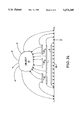
- FIG. 4b shows a perspective of the "capaciflector" camera embodiment.
- Multiple sensors 12 (12 1 -12 7 for seven rows and 12 a to 12 f for six columns) are used in conjunction with floating shield 1 and ground-coupled shield 2. Although seven rows and six columns are shown, any number of rows and columns can be used.
- sensors 12 and shields 1 (if used) and 2 are strips of conductive material with an insulative coating. Each sensor strip 12 is attached to floating shield 1 (if used) with no gap between the insulation on shield 12 and the insulation on shield 1 (or shield 2 if shield 1 is not used); likewise, shield 2 is attached to surface 15 with no gap between the insulation on shield 2 and surface 15.
- FIG. 1a is a circuit diagram of a prior art "capaciflector” using capacitively-controlled oscillator technology.
- FIG. 1b shows the prior art “capaciflector” principle.
- FIG. 1c is a schematic diagram of a current-measuring voltage follower circuit.
- FIG. 2 is a circuit diagram of a source-locked "capaciflector" utilizing current-measuring voltage follower circuits.
- FIG. 3a is a schematic diagram of a multiple sensor "capaciflector" circuit utilizing current-measuring voltage follower circuits.
- FIG. 3b is a diagram of the multiple sensor fields of FIG. 3a.
- FIG. 4a is a schematic diagram of the "capaciflector" camera parasitic capacitances.
- FIG. 4b is a perspective view of the "capaciflector" camera elements.
- FIG. 4c is a perspective view of an alternate embodiment of the "capaciflector" camera elements.
- FIG. 4d is a perspective view of another alternate embodiment of the "capaciflector" camera elements.
- FIG. 5a is a circuit diagram of a classic Wheatstone bridge utilized in the prior art.
- FIG. 5b is a circuit diagram of an active current bridge.
- FIG. 6 is a schematic diagram of an alternate embodiment "capaciflector" camera using active current bridge sensor array circuits.
- FIG. 7 is a circuit diagram of an active current bridge sensor array.
- the “capaciflector” camera sensor will be a fundamental building block of NASA robotics for use in berthing and docking for robotic construction, assembly and maintenance in outer space and for imaging and navigation for planetary rover robots.
- the ability to place individual "capaciflector” sensors in close proximity to each other as a “capaciflector” camera enables docking and berthing pins, and holes and latches to be precisely imaged in 3-D. Since the "capaciflector” camera gives monotonically accelerating stronger signals as it is closer to an object, the “capaciflector” camera will give very precise images in close to the object, the very region where other imaging techniques, such as standard cameras and lasers have problems.
- capacitive-based sensors are retained in this new embodiment of the original "capaciflector" which is described in detail in U.S. Pat. No. 5,166,679 and shown schematically in FIG. 1a where a capacitive proximity sensing element 12, backed by a reflector shield 2 driven by op-amp 4 at the same voltage as and in phase with sensor 12, is used to reflect the field lines away from a grounded surface 15 towards an intruding object 10.
- the output signal from sensor 12 is coupled to capacitively controlled oscillator circuit 3 whose output is inversely proportional to the capacitance of sensor 12.
- FIG. 1c An electronic circuit architecture is disclosed in my "Current-Measuring Op-amp Devices" U.S. patent application, referenced above, that is particularly useful in my "capaciflector” camera.
- the innovative circuit element is called a current measuring voltage follower and is shown in FIG. 1c.
- op-amp 4 is, in effect, a micro-miniature precision high-gain servo system, source 28 voltage V s , at the + terminal of op-amp 4, is served through op-amp 4 to its--terminal.
- both of the input terminals of op-amp 4 are of high impedance, op-amp 4 is also a current source with a low impedance output.
- the current-measuring voltage follower circuit of FIG. 1c is inserted between each of a series of sensors, and excites them by a common voltage source, the voltage drop (amplitude and phase) across the sensors will be nearly identical, and essentially the same as the voltage source. As with any feedback system, there are slight losses, but these are in microvolts and of no practical importance.
- the current through each sensor will also vary according to what it "senses” and this current changes can be “measured” by the sensors' current-measuring voltage follower circuit.
- a standard voltage follower circuit, on the other had, would supply the required sensor current, but would not “measure” it.
- FIG. 2 shows schematically a source-locked "capaciflector" sensor system that uses my current-measuring voltage follower circuit (op-amp 6, resistor 18) to interface source 28 voltage to sensor 12 and also a second one of my current-measuring voltage follower circuits (op-amp 4, resistor 16) to interface source 28 voltage to shield 2, located above grounded surface 15.
- resistors 20, 22, 24, 26 and op-amp 8 comprise reference circuit 5 which extracts a reference voltage from source 28, which is converted to a DC current by AC to DC converter 30; the signal from sensor 12 "measured” by its current measuring voltage follower circuit is converted to DC by AC to DC converter 32; the difference between these two “signals” is then amplified by amplification circuit 7 containing resistors 34, 36, 38, 40 and op-amp 14; the amplified signal is then supplied as output signal Vo to a suitable measurement/display device (not shown).
- FIG. 2 "capaciflector" circuit works for a fixed, as well as variable frequency so it is possible to use a crystal-controlled oscillator as source 28, if desired, thereby reducing frequency drift over long periods of time in outer space and to increase range and sensitivity by using a very narrow band system.
- FIG. 3a extends the FIG. 2 source-locked "capaciflector" concept to one involving several (in this case three) sensors 12 in close proximity to each other.
- FIGS. 3a and 3b also introduce the use of two reflective shields.
- sensors 12 i.e., 12 1 , 12 2 , 12 3
- each sensor 12 and shield 2 are interfaced to a common voltage source 28 by current-measuring voltage follower circuits (op amp 6 1 and resistor 18 1 for sensor 12 1 ; op amp 6 2 and resistor 18 2 for sensor 12 2 ; and op amp 6 3 and resistor 18 3 for sensor 12 3 ) then all sensors 12 as well as shield 2 are locked to voltage source 28 both in amplitude and in phase, and shield 2 "shields" all sensors 12 from ground providing the desired "capaciflector” effect.
- the additional shield 1 is a "floating" shield, which is not necessary for proper operation of this circuit, but can be added for use as an additional “sensor” if desired; it also has its own current-measuring voltage follower circuit of op amp 4 a and resistor 16 a .
- Floating shield 1 is, itself, shielded from ground by the ground coupled shield 2 so it can "see” between the individual sensors 12 to give an overall extended range reading.
- this circuit also has a reference circuit 5 and an amplification circuit 7 to complete the schematic.
- each sensor 12 "sees” the other sensors as a reflecting shield and vice versa, thus eliminating cross talk between sensors 12.
- different currents pass through each sensor 12, depending upon its location relative to object 10, and each of these currents are "measured”, independently, by sensors' 12 associated current-measuring voltage follower circuit. The result is independent sensing by sensors 12 in close proximity to each other and with outstanding range and sensitivity for each sensor 12.
- FIG. 4b shows the source-locked "capaciflector” concept extended still further to an entire “capaciflector” camera embodiment.
- Multiple sensors 12 (12 1 -12 7 for seven rows and 12 a to 12 f for six columns) are used in conjunction with floating shield 1 and ground-coupled shield 2. Although seven rows and six columns are shown, any number of rows and columns can be used.
- sensors 12 and shields 1 (if used) and 2 are strips of conductive material with an insulative coating. Each sensor strip 12 is attached to floating shield 1 (if used) with no gap between the insulation on sensor 12 and the insulation on shield 1 (or shield 2 if shield 1 is not used); likewise, shield 2 is attached to surface 15 with no gap between the insulation on shield 2 and surface 15.
- the potential difference between any sensor 12 and ground through these parasitics is less than 50 micro volts.
- Each current-measuring voltage follower circuit tracks the voltage across its resistive load to within 100 ⁇ V of source 28 voltage.
- a leakage field of 20 mV/in. from one sensor 12 to adjacent sensor 12 and from any sensor 12 to shield 1 exists.
- a ground return leakage voltage of 2.6 V/in. is typical.
- the ground return leakage is therefore 130 times that of the leakage caused by the current-measuring voltage follower circuits.
- a 20 mV/in. field is induced at a range of approx. 33 ft. when a 1 ft. range is required.
- FIG. 4c shows an alternate embodiment "capaciflector” camera to that depicted in FIG. 4b.
- multiple sensors 12 (12 1 -12 3 for three rows and 12 a to 12 d for four columns) are used in conjunction with ground-coupled shield 2. Although three rows and four columns are shown, any number of rows and columns can be used.
- sensors 12 and shield 2 are strips of conductive material with an insulative coating. Although not shown, a floating shield could also be used in this embodiment.
- Each sensor strip 12 is attached to shield 2 with no gap between the insulation on sensor 12 and the insulation on shield 2; likewise, shield 2 is attached to surface 15 with no gap between the insulation on shield 2 and surface 15.
- FIG. 4d shows another alternate embodiment "capaciflector” camera to that depicted in FIG. 4b.
- multiple sensors 12 (12 1 -12 5 for five rows and 12 a to 12 c for three columns) are used in conjunction with ground-coupled shield 2. Although five rows and three columns are shown, any number of rows and columns can be used.
- sensors 12 and shield 2 are strips of conductive material with an insulative coating. Although not shown, a floating shield could also be used in this embodiment.
- Each sensor strip 12 is attached to shield 2 with no gap between the insulation on sensor 12 and the insulation on shield 2; likewise, shield 2 is attached to surface 15 with no gap between the insulation on shield 2 and surface 15.
- each sensor strip 12 is compensated for by sensor row columns 12 spaced larger apart than the sensor row strips 12 as shown.
- This sensor array of five rows and three columns behaves nearly the same as described for the multiple sensors shown in FIG. 4b. A minimum amount of simple calibration will be needed with this design.
- a classic Wheatstone bridge circuit normally performs the role in signal detection now performed by an active current bridge in the alternate embodiment of the "capaciflector" camera shown in FIG. 6.
- a classic Wheatstone bridge operates as a voltage divider.
- the voltage down the left leg is identical to that down the right.
- the voltage down the left leg divides according to the impedances Z 1 and Z 4 at point A and that down the right leg divides according to the impedances Z 2 and Z 3 at point B.
- Z 4 varies (as in the case of a sensor) the voltage difference between points A and B changes and the voltage meter joining these two points reflects that change.
- this difference in potential results in leakage (or crosstalk). This can be a very significant problem which increases as the imbalance grows (as in very high sensor readings).
- the active current bridge shown in FIG. 5b arranges current-measuring voltage follower circuits and impedances in a bridge configuration similar to the Wheatstone bridge.
- the voltage across points A and B is always equal no matter how much Z 4 varies.
- leakage (or crosstalk) is significantly reduced. This condition holds true even at very high sensor readings.
- FIG. 6 shows an alternate embodiment of my "capaciflector” camera using current-measuring voltage follower circuits in an active current bridge arrangement (in contrast to a Wheatstone bridge arrangement).
- Capacitors 20 and 21 1 , 21 2 , 21 3 are used in the current-measuring voltage follower circuits (rather than resistors) for the current "measuring" function to eliminate the phase shift between the voltage measured directly at the output of current-measuring op-amps 4 a and 6 1 , 6 2 , 6 3 and source 28 voltage, no matter how object 10 to sensor 12 proximity changes.
- the parallel resistors R b which accompany each of these capacitors is very large and serves only to permit op-amp bias currents to bleed off. It is also possible to adjust the R b and capacitors values to provide a nominal phase shift value if desired. This would be useful in phase measuring schemes.
- FIG. 5b illustrates the active current bridge used in the FIG. 6 alternate embodiment.
- common voltage source 28 is fed into a left and right current-measuring voltage follower which form the first element of the left leg and the first element of the right leg respectively.
- the left leg current, I L1 is generated by the left current-measuring voltage follower and the right leg current, I L2 , by the right current-measuring voltage follower.
- the left leg current proceeds through reference Z 1 to point A and from there across reference Z 3 to ground.
- the right leg current proceeds through reference Z 2 to point B and from there across unknown impedance Z 4 to ground.
- the voltage drop from points A and B to ground are identical and equal to the source 28 voltage V s .
- the right leg current, I L2 is adjusted by the right leg op-amp as Z 4 changes to keep the voltage drop across Z 4 locked to V s . This, however, changes the voltage across reference Z 2 .
- FIG. 7 shows how the active current bridge is utilized in the alternate embodiment "capaciflector" camera of FIG. 6.
- current-measuring capacitors 20 are installed in the current-measuring voltage follower circuits.
- a capacitor in a current-measuring voltage follower tends to integrate the offset voltages of op-amp 6, thus a large charge-bleeding resistor R b is inserted in parallel with capacitor 20.
- the common reference leg of the bridge consists of a current-measuring voltage follower circuit which is identical with the other bridge legs and a reference capacitive load C Ref1 which is the average of the sensor 12 element loads (except that it is not effected by the approach of an object) and a reference current-measuring capacitor 50 which is the average of the current-measuring capacitors 50.
- Each sensor 12 element acts as a bridge leg and is compared with the reference leg as is the floating shield leg. There is one bridge (complete with reference leg) for the rows and one for the columns.
- the floating shield 1 will be the leg of either the column or the row bridge.
- the ground-coupled shield 2 will not be compared and so will not belong to either bridge.
- Each bridge will also have a second thermal drift reference current-measuring voltage follower circuit and reference capacitive load, but with a slight bridge voltage between the two reference legs leading to a reference voltage all the way through the amplification system. This voltage can change only as a result of thermal changes in the reference components and, so, gives an indication of the thermal drift in the rest of the bridge.
Abstract
A capacitive type proximity sensor having improved range and sensitivity between a surface and an intruding object in the vicinity of the surface having a voltage source, a number of outer electrical conductors on the surface with each forming one electrode of a number of sensor capacitors, the other electrode for each sensor capacitor being the object. The outer conductors are made from thin sheets of conductive material covered with insulation. An intermediate electrical conductor is located between the outer conductors and the surface and is of a size larger than the outer conductors to act as a shield for reducing the parasitic capacitance between the outer conductors and the surface. The intermediate conductor is also made from a thin sheet of conductive material covered with insulation. The outer conductors and the intermediate conductor are attached to the surface with no gap between the insulation on the conductors and no gap between the surface and the insulation on intermediate conductor, the outer conductors and the intermediate conductor conjoining with each other and with the surface, with the surface acting as a ground plane. A current-measuring voltage follower circuit is connected to the voltage source for coupling in phase and amplitude the instantaneous voltage at the voltage source to the outer electrical conductors and the intermediate electrical conductor. This circuit is responsive to the change in capacitance of the sensor capacitors and generates a number of output signals.
Description
The invention described herein was made by an employee of the United States Government, and may be manufactured and used by or for the Government for governmental purposes without the payment of any royalties thereon or therefor.
This invention is related to an invention shown and described in (1) U.S. Ser. No. 07/889,577 entitled "Phase Discriminating Capacitive Array Sensor System", filed in the name of John M. Vranish, the present inventor, on May 28, 1992now U.S. Pat. No. 5,214,388, issued May 25, 1993; (2) U.S. Ser. No. 07/979,987 entitled "Steering Capaciflector Sensor" filed in the name of Jenstrom et al. on Nov. 23, 1992; (3) U.S. Ser. No. 08/008,426 entitled "Double-Driven Shield Capaciflector Type Proximity Sensor", filed in the name of John M. Vranish the present inventor, on Jan. 25, 1993; (4) U.S. Ser. No. 08189,344 entitled "Current Measuring Op-amp Devices" filed in the name of John M. Vranish, the present inventor, on Jan. 31, 1994. The above are assigned to the assignee of the present invention. Moreover, the teachings of these related applications is herein meant to be incorporated by reference.
This invention relates to capacitive proximity sensors and more particularly to a capacitive sensor that will permit 3-D imaging by electrically scanning rows and columns useful for collision avoidance situations.
Capacitive-Controlled Oscillator (CCO) based "capaciflector" proximity sensors and CCO based sensor arrays are available (see FIG. 1a and U.S. Pat. No. 5,166,679 for a discussion of the basic "capaciflector" technology). However, CCO based "capaciflector" sensors can be used as arrays only where the separation between individual sensors can be made large, such as 3 to 6 inches. Also, for a "capaciflector" sensor to perform efficiently, the shield must be much larger that the sensor (on the order of 7 times wider) and each sensor must have its own shield. The shield is slaved to the sensor via a voltage follower, so it changes frequency with the sensor. If another sensor is introduced, another CCO and voltage follower shield must be added. Hence, the sensors must be spaced no closer than the width of the shields. Even then, there is some cross talk because the two sensors are out of phase with each other. This application is satisfactory for collision avoidance arrays and rudimentary alignment, but an entirely new approach is necessary for a "capaciflector" camera.
Tactile capacitive arrays using pixels are also available in the research environment and appear to be practical for medical and industrial applications. However, these devices have such a short range that they would not have the depth of view necessary for good capacitive 3-D proximity images and they would be impractical for robotic collision avoidance purposes (frequently part of the "capaciflector" camera imaging function). Also, without the current-measuring voltage follower electronics architecture described in this disclosure (and an active current bridge version of the same), there will be cross talk between the pixels and/or their leads.
"Capaciflector" 3-D imaging using a single sensor has also been achieved in the prior art. In this application, the single "capaciflector" sensor is moved through a volume with sensor readings being taken sequentially in the process. These readings are compared with the robot joint angles and a 3-D image results. There are three disadvantages to this type of system; first, large volumes often must be swept out in order to obtain a complete picture and this may not be possible or practical in a docking or berthing application; second, the process takes a considerable amount of time; and third, the measurements must be correlated with robot joint angle information which introduces further inaccuracies.
It is therefore an object of the present invention to provide a sensor with multiple, independently-sensing "capaciflector" sensors in close proximity to each other sharing a common reflecting shield to facilitate robotic collision avoidance and berthing/docking.
Another object of the present invention is to provide a capacitive camera that will provide a 3-D image to give a robot a physical model of the region being observed by the camera.
A further object is to provide a sensor with a narrow bandwidth thereby providing increased range and sensitivity with less noise and EMI problems than current devices.
These and other objects are achieved by providing a device with several sensors placed in close proximity to each other above a driven shield with each sensor and shield interfaced to a common voltage source by current-measuring voltage follower circuits. All sensors and the shield are thus locked to the voltage source both in amplitude and in phase, and the shield "shields" all sensors from ground providing the desired "capaciflector" effect. An additional shield can be added and is a "floating" shield, which is not necessary for proper operation of this circuit, but can be added for use as an additional "sensor" if desired; it also has its own current-measuring voltage follower circuit. The floating shield is, itself, shielded from ground by the ground-coupled shield so it can "see" between the individual sensors to give an overall extended range reading. This device also has a reference circuit and an amplification circuit to further process the signals from the sensors and provide an output which can be utilized as a control signal.
Functionally there is no difference between the shield and the sensors so each sensor "sees" the other sensors as a reflecting shield and vice versa, thus eliminating cross talk between the sensors. As an object approaches the sensors, different currents pass through each sensor, depending upon its location relative to the object, and each of these currents are "measured", independently, by the sensors' associated current-measuring voltage follower circuit. The result is independent sensing by the sensors in close proximity to each other and with outstanding range and sensitivity for each sensor.
FIG. 4b shows a perspective of the "capaciflector" camera embodiment. Multiple sensors 12 (121 -127 for seven rows and 12a to 12f for six columns) are used in conjunction with floating shield 1 and ground-coupled shield 2. Although seven rows and six columns are shown, any number of rows and columns can be used. As in the original "capaciflector" sensors 12 and shields 1 (if used) and 2 are strips of conductive material with an insulative coating. Each sensor strip 12 is attached to floating shield 1 (if used) with no gap between the insulation on shield 12 and the insulation on shield 1 (or shield 2 if shield 1 is not used); likewise, shield 2 is attached to surface 15 with no gap between the insulation on shield 2 and surface 15. In order to have both rows and columns, it is necessary to have sensor strips 12 pass over and under each other in the weave geometry shown. This sensor array of seven rows and six columns behaves exactly as described for the multiple sensors shown in FIGS. 3a and 3b except that each sensor strip 12 must alternately pass over and under other sensor strips 12. As described above, each sensor strip 12 "sees" the other sensor strips as shields, so the presence of these other sensor strips will be insignificant in terms of leakage.
FIG. 1a is a circuit diagram of a prior art "capaciflector" using capacitively-controlled oscillator technology.
FIG. 1b shows the prior art "capaciflector" principle.
FIG. 1c is a schematic diagram of a current-measuring voltage follower circuit.
FIG. 2 is a circuit diagram of a source-locked "capaciflector" utilizing current-measuring voltage follower circuits.
FIG. 3a is a schematic diagram of a multiple sensor "capaciflector" circuit utilizing current-measuring voltage follower circuits.
FIG. 3b is a diagram of the multiple sensor fields of FIG. 3a.
FIG. 4a is a schematic diagram of the "capaciflector" camera parasitic capacitances.
FIG. 4b is a perspective view of the "capaciflector" camera elements.
FIG. 4c is a perspective view of an alternate embodiment of the "capaciflector" camera elements.
FIG. 4d is a perspective view of another alternate embodiment of the "capaciflector" camera elements.
FIG. 5a is a circuit diagram of a classic Wheatstone bridge utilized in the prior art.
FIG. 5b is a circuit diagram of an active current bridge.
FIG. 6 is a schematic diagram of an alternate embodiment "capaciflector" camera using active current bridge sensor array circuits.
FIG. 7 is a circuit diagram of an active current bridge sensor array.
The "capaciflector" camera sensor will be a fundamental building block of NASA robotics for use in berthing and docking for robotic construction, assembly and maintenance in outer space and for imaging and navigation for planetary rover robots. The ability to place individual "capaciflector" sensors in close proximity to each other as a "capaciflector" camera enables docking and berthing pins, and holes and latches to be precisely imaged in 3-D. Since the "capaciflector" camera gives monotonically accelerating stronger signals as it is closer to an object, the "capaciflector" camera will give very precise images in close to the object, the very region where other imaging techniques, such as standard cameras and lasers have problems. And, because several "capaciflector" camera sensors can be placed on or near pins, latches and holes, the information available at or near the points of contact between the payload and the fixture it is being mated to will be exceptionally good. For exploration robots, the "capaciflector" camera will provide close-in images which will prove invaluable in obstacle avoidance and navigation.
The fundamental advantages of capacitive-based sensors are retained in this new embodiment of the original "capaciflector" which is described in detail in U.S. Pat. No. 5,166,679 and shown schematically in FIG. 1a where a capacitive proximity sensing element 12, backed by a reflector shield 2 driven by op-amp 4 at the same voltage as and in phase with sensor 12, is used to reflect the field lines away from a grounded surface 15 towards an intruding object 10. The output signal from sensor 12 is coupled to capacitively controlled oscillator circuit 3 whose output is inversely proportional to the capacitance of sensor 12. The advantages of this type sensor system include: a simple, rugged, flexible configuration that can fit on the surface of any structure; ability of the system to function in outer space; the ability to sense virtually any object it encounters; the ability of the sensor to "see" through paint and other protective coatings; and, low power. The previous problem of inadequate range has also been solved by "capaciflector" technology.
An electronic circuit architecture is disclosed in my "Current-Measuring Op-amp Devices" U.S. patent application, referenced above, that is particularly useful in my "capaciflector" camera. The innovative circuit element is called a current measuring voltage follower and is shown in FIG. 1c. Because op-amp 4 is, in effect, a micro-miniature precision high-gain servo system, source 28 voltage Vs, at the + terminal of op-amp 4, is served through op-amp 4 to its--terminal. Although both of the input terminals of op-amp 4 are of high impedance, op-amp 4 is also a current source with a low impedance output. Therefore, if the current-measuring voltage follower circuit of FIG. 1c is inserted between each of a series of sensors, and excites them by a common voltage source, the voltage drop (amplitude and phase) across the sensors will be nearly identical, and essentially the same as the voltage source. As with any feedback system, there are slight losses, but these are in microvolts and of no practical importance. The current through each sensor will also vary according to what it "senses" and this current changes can be "measured" by the sensors' current-measuring voltage follower circuit. A standard voltage follower circuit, on the other had, would supply the required sensor current, but would not "measure" it.
FIG. 2 shows schematically a source-locked "capaciflector" sensor system that uses my current-measuring voltage follower circuit (op-amp 6, resistor 18) to interface source 28 voltage to sensor 12 and also a second one of my current-measuring voltage follower circuits (op-amp 4, resistor 16) to interface source 28 voltage to shield 2, located above grounded surface 15. This effectively locks both sensor 12 and shield 2 to source 28 voltage, and to each other, and therefore shield 2 electrical fields serve to block the path of sensor 12 electrical fields to ground, resulting in a "capaciflector" action and with it increased range and sensitivity. The remaining components of FIG. 2 represent standard electronic circuits; resistors 20, 22, 24, 26 and op-amp 8 comprise reference circuit 5 which extracts a reference voltage from source 28, which is converted to a DC current by AC to DC converter 30; the signal from sensor 12 "measured" by its current measuring voltage follower circuit is converted to DC by AC to DC converter 32; the difference between these two "signals" is then amplified by amplification circuit 7 containing resistors 34, 36, 38, 40 and op-amp 14; the amplified signal is then supplied as output signal Vo to a suitable measurement/display device (not shown).
With the approach of object 10, current through sensor 12 increases and this increased current is detected by a change in voltage across resistor 18 in sensor 12's current-measuring voltage follower circuit. Shield 2 will also "see" object 10, and its increased current flow through resistor 16 can also be detected, if desired, although this is not shown on FIG. 2. The FIG. 2 "capaciflector" circuit works for a fixed, as well as variable frequency so it is possible to use a crystal-controlled oscillator as source 28, if desired, thereby reducing frequency drift over long periods of time in outer space and to increase range and sensitivity by using a very narrow band system.
The circuit shown in FIG. 3a extends the FIG. 2 source-locked "capaciflector" concept to one involving several (in this case three) sensors 12 in close proximity to each other. FIGS. 3a and 3b also introduce the use of two reflective shields. As shown, if several sensors 12 (i.e., 121, 122, 123) are placed in close proximity to each other above driven shield 2 and if each sensor 12 (and shield 2) are interfaced to a common voltage source 28 by current-measuring voltage follower circuits (op amp 61 and resistor 181 for sensor 121 ; op amp 62 and resistor 182 for sensor 122 ; and op amp 63 and resistor 183 for sensor 123) then all sensors 12 as well as shield 2 are locked to voltage source 28 both in amplitude and in phase, and shield 2 "shields" all sensors 12 from ground providing the desired "capaciflector" effect. The additional shield 1 is a "floating" shield, which is not necessary for proper operation of this circuit, but can be added for use as an additional "sensor" if desired; it also has its own current-measuring voltage follower circuit of op amp 4a and resistor 16a. Floating shield 1 is, itself, shielded from ground by the ground coupled shield 2 so it can "see" between the individual sensors 12 to give an overall extended range reading. Although not explicitly shown, just as in FIG. 2 this circuit also has a reference circuit 5 and an amplification circuit 7 to complete the schematic.
Functionally there is no difference between shield 2 and sensors 12 so each sensor 12 "sees" the other sensors as a reflecting shield and vice versa, thus eliminating cross talk between sensors 12. As object 10 approaches sensors 12, different currents pass through each sensor 12, depending upon its location relative to object 10, and each of these currents are "measured", independently, by sensors' 12 associated current-measuring voltage follower circuit. The result is independent sensing by sensors 12 in close proximity to each other and with outstanding range and sensitivity for each sensor 12.
FIG. 4b shows the source-locked "capaciflector" concept extended still further to an entire "capaciflector" camera embodiment. Multiple sensors 12 (121 -127 for seven rows and 12a to 12f for six columns) are used in conjunction with floating shield 1 and ground-coupled shield 2. Although seven rows and six columns are shown, any number of rows and columns can be used. As in the original "capaciflector", sensors 12 and shields 1 (if used) and 2 are strips of conductive material with an insulative coating. Each sensor strip 12 is attached to floating shield 1 (if used) with no gap between the insulation on sensor 12 and the insulation on shield 1 (or shield 2 if shield 1 is not used); likewise, shield 2 is attached to surface 15 with no gap between the insulation on shield 2 and surface 15. In order to have both rows and columns, with equal access to the object by each, it is necessary to have sensor strips 12 pass over and under each other in the weave geometry shown. This sensor array of seven rows and six columns behaves exactly as described for the multiple sensors shown in FIGS. 3a and 3b except that each sensor strip 12 must alternately pass over and under other sensor strips 12. As described above, each sensor strip 12 "sees" the other sensor strips as shields, so the presence of these other sensor strips will be insignificant in terms of leakage.
The parasitic capacitances for a single sensor strip 12 of the FIG. 4b embodiment are given in the equivalent circuit shown in FIG. 4a where the dashed lines represent leakages to other elements and:
Cso = sensor to object capacitance
Cog = object to ground capacitance (assumed to be large)
Csg = sensor to ground capacitance (typically approx. 6 pf)
CHI = sensor to High Impedance shield capacitance (typ. approx. 120 pf)
CIG = High Impedance Shield to ground capacitance (typ. approx. 800 pf)
COTO = secondary sensor to object capacitance (typ. approx. 6 pf)
COTG = secondary sensor to ground capacitance (typ. approx. 6 pf)
COT = sensor to secondary sensor capacitance
The potential difference between any sensor 12 and ground through these parasitics is less than 50 micro volts.
Current leakage in the "capaciflector" camera is not noticeably reduced from that of a single sensor "capaciflector". Each current-measuring voltage follower circuit tracks the voltage across its resistive load to within 100 μV of source 28 voltage. Using an insulation separation between sensor strips passing over and under each other of 0.005 in., a leakage field of 20 mV/in. from one sensor 12 to adjacent sensor 12 and from any sensor 12 to shield 1 exists. Assuming a minimum or worst case distance of 3 in. from the edge of shield 2 and assuming a maximum load voltage (typical) of 8 V, a ground return leakage voltage of 2.6 V/in. is typical. The ground return leakage is therefore 130 times that of the leakage caused by the current-measuring voltage follower circuits. For an object 10 approaching the "capaciflector" camera, a 20 mV/in. field is induced at a range of approx. 33 ft. when a 1 ft. range is required. These figures represent worst case assumptions. Leakage between sensor 12 strips and or shield 2 requires the charge to leak across at least two shields in series so the real leakage field is orders of magnitude below 20 Mv/in.
FIG. 4c shows an alternate embodiment "capaciflector" camera to that depicted in FIG. 4b. In this embodiment, multiple sensors 12 (121 -123 for three rows and 12a to 12d for four columns) are used in conjunction with ground-coupled shield 2. Although three rows and four columns are shown, any number of rows and columns can be used. As in the FIG. 4b "capaciflector" camera, sensors 12 and shield 2 are strips of conductive material with an insulative coating. Although not shown, a floating shield could also be used in this embodiment. Each sensor strip 12 is attached to shield 2 with no gap between the insulation on sensor 12 and the insulation on shield 2; likewise, shield 2 is attached to surface 15 with no gap between the insulation on shield 2 and surface 15. In order to compensate for the unequal access to the object by each sensor strip 12, it is necessary to have sensor row strips 12 larger the sensor column strips 12 as shown. This sensor array of three rows and four columns behaves nearly the same as described for the multiple sensors shown in FIG. 4b. A minimum amount of simple calibration will be needed with this design.
FIG. 4d shows another alternate embodiment "capaciflector" camera to that depicted in FIG. 4b. In this embodiment, multiple sensors 12 (121 -125 for five rows and 12a to 12c for three columns) are used in conjunction with ground-coupled shield 2. Although five rows and three columns are shown, any number of rows and columns can be used. As in the FIG. 4b "capaciflector" camera, sensors 12 and shield 2 are strips of conductive material with an insulative coating. Although not shown, a floating shield could also be used in this embodiment. Each sensor strip 12 is attached to shield 2 with no gap between the insulation on sensor 12 and the insulation on shield 2; likewise, shield 2 is attached to surface 15 with no gap between the insulation on shield 2 and surface 15. In this embodiment, the unequal access to the object by each sensor strip 12 is compensated for by sensor row columns 12 spaced larger apart than the sensor row strips 12 as shown. This sensor array of five rows and three columns behaves nearly the same as described for the multiple sensors shown in FIG. 4b. A minimum amount of simple calibration will be needed with this design.
A classic Wheatstone bridge circuit, as shown in FIG. 5a, normally performs the role in signal detection now performed by an active current bridge in the alternate embodiment of the "capaciflector" camera shown in FIG. 6. A classic Wheatstone bridge operates as a voltage divider. The voltage down the left leg is identical to that down the right. The voltage down the left leg divides according to the impedances Z1 and Z4 at point A and that down the right leg divides according to the impedances Z2 and Z3 at point B. Thus, as Z4 varies (as in the case of a sensor) the voltage difference between points A and B changes and the voltage meter joining these two points reflects that change. For two sensors (or a sensor and a reference), this difference in potential results in leakage (or crosstalk). This can be a very significant problem which increases as the imbalance grows (as in very high sensor readings).
The active current bridge shown in FIG. 5b arranges current-measuring voltage follower circuits and impedances in a bridge configuration similar to the Wheatstone bridge. In the FIG. 5b circuit the voltage across points A and B is always equal no matter how much Z4 varies. Thus, leakage (or crosstalk) is significantly reduced. This condition holds true even at very high sensor readings.
FIG. 6 shows an alternate embodiment of my "capaciflector" camera using current-measuring voltage follower circuits in an active current bridge arrangement (in contrast to a Wheatstone bridge arrangement). Capacitors 20 and 211, 212, 213 are used in the current-measuring voltage follower circuits (rather than resistors) for the current "measuring" function to eliminate the phase shift between the voltage measured directly at the output of current-measuring op- amps 4a and 61, 62, 63 and source 28 voltage, no matter how object 10 to sensor 12 proximity changes. The parallel resistors Rb, which accompany each of these capacitors is very large and serves only to permit op-amp bias currents to bleed off. It is also possible to adjust the Rb and capacitors values to provide a nominal phase shift value if desired. This would be useful in phase measuring schemes.
FIG. 5b illustrates the active current bridge used in the FIG. 6 alternate embodiment. In the active current bridge, common voltage source 28 is fed into a left and right current-measuring voltage follower which form the first element of the left leg and the first element of the right leg respectively. The left leg current, IL1, is generated by the left current-measuring voltage follower and the right leg current, IL2, by the right current-measuring voltage follower. The left leg current proceeds through reference Z1 to point A and from there across reference Z3 to ground. The right leg current proceeds through reference Z2 to point B and from there across unknown impedance Z4 to ground. The voltage drop from points A and B to ground are identical and equal to the source 28 voltage Vs. The right leg current, IL2, is adjusted by the right leg op-amp as Z4 changes to keep the voltage drop across Z4 locked to Vs. This, however, changes the voltage across reference Z2. Thus, there is a voltage differential between the voltage drop across Z2 and that across Z1 and it is here where the bridge measurement is made. The differential voltage measurement is in front of impedances Z1 and Z2 in the active current bridge and is behind those impedances in the classical Wheatstone bridge. Is ≈0 for the active current bridge, whereas Is =IL1 +IL2 for the classical Wheatstone bridge.
FIG. 7 shows how the active current bridge is utilized in the alternate embodiment "capaciflector" camera of FIG. 6. To reduce the effects of phase shifts in the bridge, with its capacitive loads, current-measuring capacitors 20 are installed in the current-measuring voltage follower circuits. A capacitor in a current-measuring voltage follower tends to integrate the offset voltages of op-amp 6, thus a large charge-bleeding resistor Rb is inserted in parallel with capacitor 20. The common reference leg of the bridge consists of a current-measuring voltage follower circuit which is identical with the other bridge legs and a reference capacitive load CRef1 which is the average of the sensor 12 element loads (except that it is not effected by the approach of an object) and a reference current-measuring capacitor 50 which is the average of the current-measuring capacitors 50. Each sensor 12 element acts as a bridge leg and is compared with the reference leg as is the floating shield leg. There is one bridge (complete with reference leg) for the rows and one for the columns. The floating shield 1 will be the leg of either the column or the row bridge. The ground-coupled shield 2 will not be compared and so will not belong to either bridge. Each bridge will also have a second thermal drift reference current-measuring voltage follower circuit and reference capacitive load, but with a slight bridge voltage between the two reference legs leading to a reference voltage all the way through the amplification system. This voltage can change only as a result of thermal changes in the reference components and, so, gives an indication of the thermal drift in the rest of the bridge.
To those skilled in the art, many modifications and variations of the present invention are possible in light of the above teachings. It is therefore to be understood that the present invention can be practiced otherwise than as specifically described herein and still will be within the spirit and scope of the appended claims.
Claims (8)
1. A capacitive type proximity sensor having improved range and sensitivity between a surface and an intruding object in the vicinity of the surface comprising:
a voltage source;
a plurality of outer electrical conductors on said surface each forming one electrode of a plurality of sensor capacitors, the other electrode for each sensor capacitor comprising said object, said plurality of outer conductors comprising thin strips of conductive material covered with insulation and arranged in rows and columns;
an intermediate electrical conductor located between said plurality of outer conductors and said surface and being of a size larger than said plurality of outer conductors to act as a shield for reducing the parasitic capacitance between said plurality of outer conductors and said surface, said intermediate conductor comprising a thin sheet of conductive material covered with insulation;
said plurality of outer conductors and said intermediate conductor attached to said surface with no gap between the insulation on said conductors and no gap between said surface and the insulation on said intermediate conductor, said plurality of outer conductors and said intermediate conductor conjoining with each other and with said surface, said surface acting as a ground plane; and
measurement circuit means, connected to said voltage source, for coupling in phase and amplitude the instantaneous voltage at said voltage source to said plurality of outer electrical conductors and said intermediate electrical conductor, said measurement circuit means responsive to the change in capacitance of said plurality of sensor capacitors for generating a plurality of output signals.
2. The sensor of claim 1 wherein said thin strips arranged in rows and columns are arranged in a basket weave fashion.
3. The sensor of claim 1 wherein said thin strips arranged in rows and columns are arranged such that the rows are underneath the columns with the row strips wider than the column strips.
4. The sensor of claim 1 wherein said thin strips arranged in rows and columns are arranged such that the rows are underneath the columns with the spacing between the column strips wider than the spacing between the row strips.
5. The sensor of claim 1 wherein said measurement circuit means comprises a plurality of current-measuring voltage follower circuits each comprised of an op-amp and a resistor.
6. The sensor of claim 1 wherein said measurement circuit means comprises a plurality of current-measuring voltage follower circuits each comprises of an op-amp, a resistor and a capacitor.
7. The sensor of claim 1 wherein said measurement circuit means comprises a plurality of active current bridge circuits.
8. The sensor of claim 1 further comprising an additional electrical conductor located between said plurality of outer electrical conductors and said intermediate electrical conductor and being of a size larger than said plurality of outer conductors but less than or equal to the size of said intermediate conductor, said additional conductor comprising a thin sheet of conductive material covered with insulation.
Priority Applications (1)
| Application Number | Priority Date | Filing Date | Title |
|---|---|---|---|
| US08/090,230 US5373245A (en) | 1993-07-12 | 1993-07-12 | Capaciflector camera |
Applications Claiming Priority (1)
| Application Number | Priority Date | Filing Date | Title |
|---|---|---|---|
| US08/090,230 US5373245A (en) | 1993-07-12 | 1993-07-12 | Capaciflector camera |
Publications (1)
| Publication Number | Publication Date |
|---|---|
| US5373245A true US5373245A (en) | 1994-12-13 |
Family
ID=22221878
Family Applications (1)
| Application Number | Title | Priority Date | Filing Date |
|---|---|---|---|
| US08/090,230 Expired - Lifetime US5373245A (en) | 1993-07-12 | 1993-07-12 | Capaciflector camera |
Country Status (1)
| Country | Link |
|---|---|
| US (1) | US5373245A (en) |
Cited By (70)
| Publication number | Priority date | Publication date | Assignee | Title |
|---|---|---|---|---|
| US5521515A (en) * | 1995-02-17 | 1996-05-28 | The United States Of America As Represented By The Administrator Of The National Aeronautics And Space Administration | Frequency scanning capaciflector for capacitively determining the material properties |
| WO1997029391A1 (en) * | 1996-02-09 | 1997-08-14 | Scandmec Ab | Device for sensing presence of an electrically conducting object |
| WO1998007051A1 (en) * | 1996-08-14 | 1998-02-19 | Breed Automotive Technology, Inc. | Phase shift detection and measurement circuit for capacitive sensor |
| US5764066A (en) * | 1995-10-11 | 1998-06-09 | Sandia Corporation | Object locating system |
| US5770997A (en) * | 1995-06-26 | 1998-06-23 | Alliedsignal Inc. | Vehicle occupant sensing system |
| WO1998030921A2 (en) * | 1997-01-06 | 1998-07-16 | Jentek Sensors, Inc. | Magnetometer and dielectrometer detection of subsurface objects |
| US5966011A (en) * | 1995-08-25 | 1999-10-12 | Jentek Sensors, Inc. | Apparatus for measuring bulk materials and surface conditions for flat and curved parts |
| US6121782A (en) * | 1997-04-09 | 2000-09-19 | Case Corporation | Method for measuring yield and moisture |
| US6188218B1 (en) | 1997-10-29 | 2001-02-13 | Jentek Sensors, Inc. | Absolute property measurement with air calibration |
| US6242927B1 (en) | 1997-04-09 | 2001-06-05 | Case Corporation | Method and apparatus measuring parameters of material |
| US6283504B1 (en) | 1998-12-30 | 2001-09-04 | Automotive Systems Laboratory, Inc. | Occupant sensor |
| US6316949B1 (en) * | 1999-01-19 | 2001-11-13 | Nidec-Read Corporation | Apparatus and method for testing electric conductivity of circuit path ways on circuit board |
| US20010045733A1 (en) * | 2000-05-26 | 2001-11-29 | Stanley James Gregory | Occupant sensor |
| US20020000977A1 (en) * | 2000-03-23 | 2002-01-03 | National Aeronautics And Space Administration | Three dimensional interactive display |
| US6348862B1 (en) | 1999-03-05 | 2002-02-19 | Automotive Systems Laboratory, Inc. | Proximity sensor |
| US6377039B1 (en) | 1997-11-14 | 2002-04-23 | Jentek Sensors, Incorporated | Method for characterizing coating and substrates |
| US6437695B1 (en) * | 1998-10-16 | 2002-08-20 | Bayerische Motoren Werke Aktiengesellschaft | Method for capacitive object recognition in vehicles |
| US6441623B1 (en) * | 1999-07-29 | 2002-08-27 | Ab Automotive Electronics Ltd. | Capacitive proximity sensor for automotive use |
| US6445294B1 (en) | 1999-07-15 | 2002-09-03 | Automotive Systems Laboratory, Inc. | Proximity sensor |
| US6486673B1 (en) | 1997-01-06 | 2002-11-26 | Jentek Sensors, Inc. | Segmented field dielectrometer |
| US6492821B1 (en) | 2000-07-31 | 2002-12-10 | Banner Engineering Corporation | Method and apparatus for detection signal processing |
| US20030013328A1 (en) * | 2001-05-22 | 2003-01-16 | Andrade Thomas L. | Connection assembly for integrated circuit sensors |
| US20030020495A1 (en) * | 2001-05-22 | 2003-01-30 | Andrade Thomas L. | Surface capacitance sensor system using buried stimulus electrode |
| US20030083795A1 (en) * | 2001-10-31 | 2003-05-01 | Automotive Systems Laboratory, Inc. | Occupant detection system |
| US6593755B1 (en) | 2000-07-31 | 2003-07-15 | Banner Engineering Corporation | Method and apparatus for detection sensor shielding |
| US20030137219A1 (en) * | 2001-12-19 | 2003-07-24 | Peter Heiligensetzer | Device and method for securing apparatuses with parts freely movable in space |
| FR2844349A1 (en) * | 2002-09-06 | 2004-03-12 | Nanotec Solution | CAPACITIVE SENSOR PROXIMITY DETECTOR |
| US20040090053A1 (en) * | 2002-11-08 | 2004-05-13 | Craig White | Airbag with bag mounted sensor |
| US20040125918A1 (en) * | 2002-12-27 | 2004-07-01 | Giridharan Shanmugavel | Proximity detector and radiography system |
| US6781387B2 (en) | 1997-01-06 | 2004-08-24 | Jentek Sensors, Inc. | Inspection method using penetrant and dielectrometer |
| US20040226800A1 (en) * | 2003-05-13 | 2004-11-18 | Credo Technology Corporation. | Safety detection and protection system for power tools |
| US6825765B2 (en) | 1998-12-30 | 2004-11-30 | Automotive Systems Laboratory, Inc. | Occupant detection system |
| US20040249584A1 (en) * | 2003-06-03 | 2004-12-09 | Gibb William J. | Adaptive proximity sensing |
| WO2005012037A2 (en) * | 2003-07-28 | 2005-02-10 | Ab Automotive Electronics Ltd. | Capacitive sensor |
| US20050068044A1 (en) * | 2001-10-24 | 2005-03-31 | William Peine | Array sensor electronics |
| US20060061354A1 (en) * | 2004-08-25 | 2006-03-23 | Wallance Daniel I | System and method for using magnetic sensors to track the position of an object |
| US20060076985A1 (en) * | 2004-08-18 | 2006-04-13 | Southwest Research Institute | Systems and methods for detection of dielectric change in material and structure |
| US20060270145A1 (en) * | 2005-05-25 | 2006-11-30 | Bach Jerome | Capacitive array |
| US7256589B2 (en) | 2001-04-27 | 2007-08-14 | Atrua Technologies, Inc. | Capacitive sensor system with improved capacitance measuring sensitivity |
| US20070268265A1 (en) * | 2006-05-18 | 2007-11-22 | Cypress Semiconductor Corporation | Two-pin buttons |
| US20070267909A1 (en) * | 2006-05-16 | 2007-11-22 | Grammer Ag | Auto-adjust vehicle headrest |
| US20080074098A1 (en) * | 2006-09-27 | 2008-03-27 | Nasa Hq's. | Device, system and method for a sensing electrical circuit |
| US20080122458A1 (en) * | 2006-11-28 | 2008-05-29 | Process Equipment Co. Of Tipp City | Proximity detection system |
| US20080179112A1 (en) * | 2007-01-30 | 2008-07-31 | Zheng Qin | Setting a discharge rate and a charge rate of a relaxation oscillator circuit |
| US20080186034A1 (en) * | 2007-02-06 | 2008-08-07 | Ingrid Scheckenbach | Capacitive occupant detection system |
| WO2008135121A1 (en) * | 2007-05-03 | 2008-11-13 | Rehau Ag + Co | Bumper for a motor vehicle having a sensor band arrangement and a method for determining the distance of the motor vehicle |
| US20090146668A1 (en) * | 2006-07-13 | 2009-06-11 | Wuerstlein Holger | Anti-pinch sensor and evaluation circuit |
| US20090146827A1 (en) * | 2007-11-30 | 2009-06-11 | Wuerstlein Holger | Anti-pinch sensor |
| WO2010060767A1 (en) | 2008-11-25 | 2010-06-03 | Huf Hülsbeck & Fürst Gmbh & Co. Kg | Capacitive proximity sensor having a shielding electrode and a diagnostic electrode |
| US20100271049A1 (en) * | 2009-04-22 | 2010-10-28 | Peter Van Gastel | Sensor electronics in a vehicle door handle |
| US8040142B1 (en) | 2006-03-31 | 2011-10-18 | Cypress Semiconductor Corporation | Touch detection techniques for capacitive touch sense systems |
| WO2011138081A1 (en) * | 2010-05-07 | 2011-11-10 | Robert Bosch Gmbh | Detection of a dielectric object |
| US8246384B1 (en) | 2008-07-25 | 2012-08-21 | Wallace Henry B | Variable capacitance audio cable |
| US20120222496A1 (en) * | 2011-03-04 | 2012-09-06 | Hm Technology International Limited | Sensor Array |
| US8321174B1 (en) | 2008-09-26 | 2012-11-27 | Cypress Semiconductor Corporation | System and method to measure capacitance of capacitive sensor array |
| US8358142B2 (en) | 2008-02-27 | 2013-01-22 | Cypress Semiconductor Corporation | Methods and circuits for measuring mutual and self capacitance |
| WO2013083952A1 (en) * | 2011-12-09 | 2013-06-13 | Hm Technology International Limited | Capacitive matrix sensor for measuring permittivity of an object |
| US8525798B2 (en) | 2008-01-28 | 2013-09-03 | Cypress Semiconductor Corporation | Touch sensing |
| US8536902B1 (en) | 2007-07-03 | 2013-09-17 | Cypress Semiconductor Corporation | Capacitance to frequency converter |
| US8547114B2 (en) | 2006-11-14 | 2013-10-01 | Cypress Semiconductor Corporation | Capacitance to code converter with sigma-delta modulator |
| US8564313B1 (en) | 2007-07-03 | 2013-10-22 | Cypress Semiconductor Corporation | Capacitive field sensor with sigma-delta modulator |
| US8570052B1 (en) | 2008-02-27 | 2013-10-29 | Cypress Semiconductor Corporation | Methods and circuits for measuring mutual and self capacitance |
| TWI482423B (en) * | 2011-07-05 | 2015-04-21 | Mediatek Singapore Pte Ltd | Clock signal generating apparatus and method used in clock signal generating apparatus |
| US9104273B1 (en) | 2008-02-29 | 2015-08-11 | Cypress Semiconductor Corporation | Multi-touch sensing method |
| US9417728B2 (en) | 2009-07-28 | 2016-08-16 | Parade Technologies, Ltd. | Predictive touch surface scanning |
| US9500686B1 (en) | 2007-06-29 | 2016-11-22 | Cypress Semiconductor Corporation | Capacitance measurement system and methods |
| JP2017096934A (en) * | 2015-11-20 | 2017-06-01 | ゼネラル・エレクトリック・カンパニイ | Systems and methods for measuring component strain |
| JP2019095356A (en) * | 2017-11-24 | 2019-06-20 | 島根県 | Electrode expansion type electrostatic capacitive sensor |
| WO2019214769A1 (en) * | 2018-05-07 | 2019-11-14 | Kinotex Sensor Gmbh | Device and method for protecting a mobile appliance under machine or automatic control, and sensor tile |
| US20210318186A1 (en) * | 2018-03-30 | 2021-10-14 | Panasonic Intellectual Property Management Co., Ltd. | Capacitance detection device |
Citations (6)
| Publication number | Priority date | Publication date | Assignee | Title |
|---|---|---|---|---|
| US4908574A (en) * | 1986-09-03 | 1990-03-13 | Extrude Hone Corporation | Capacitor array sensors for determining conformity to surface shape |
| US4922181A (en) * | 1987-08-06 | 1990-05-01 | Laetus Systems Limited | Apparatus for monitoring the dielectric constant of an article |
| US4992741A (en) * | 1986-03-27 | 1991-02-12 | The Stanley Works | Capacitive sensor and metal detector with a display for quantitatively displaying signals resulting from concealed objects |
| US5097216A (en) * | 1990-10-09 | 1992-03-17 | Agr International, Inc. | Apparatus for inspecting the wall thickness of a container and corresponding method |
| US5166679A (en) * | 1991-06-06 | 1992-11-24 | The United States Of America As Represented By The Administrator Of The National Aeronautics & Space Administration | Driven shielding capacitive proximity sensor |
| US5214388A (en) * | 1992-05-28 | 1993-05-25 | The United States Of America As Represented By The Administrator Of The National Aeronautics And Space Administration | Phase discriminating capacitive array sensor system |
-
1993
- 1993-07-12 US US08/090,230 patent/US5373245A/en not_active Expired - Lifetime
Patent Citations (6)
| Publication number | Priority date | Publication date | Assignee | Title |
|---|---|---|---|---|
| US4992741A (en) * | 1986-03-27 | 1991-02-12 | The Stanley Works | Capacitive sensor and metal detector with a display for quantitatively displaying signals resulting from concealed objects |
| US4908574A (en) * | 1986-09-03 | 1990-03-13 | Extrude Hone Corporation | Capacitor array sensors for determining conformity to surface shape |
| US4922181A (en) * | 1987-08-06 | 1990-05-01 | Laetus Systems Limited | Apparatus for monitoring the dielectric constant of an article |
| US5097216A (en) * | 1990-10-09 | 1992-03-17 | Agr International, Inc. | Apparatus for inspecting the wall thickness of a container and corresponding method |
| US5166679A (en) * | 1991-06-06 | 1992-11-24 | The United States Of America As Represented By The Administrator Of The National Aeronautics & Space Administration | Driven shielding capacitive proximity sensor |
| US5214388A (en) * | 1992-05-28 | 1993-05-25 | The United States Of America As Represented By The Administrator Of The National Aeronautics And Space Administration | Phase discriminating capacitive array sensor system |
Cited By (140)
| Publication number | Priority date | Publication date | Assignee | Title |
|---|---|---|---|---|
| US5521515A (en) * | 1995-02-17 | 1996-05-28 | The United States Of America As Represented By The Administrator Of The National Aeronautics And Space Administration | Frequency scanning capaciflector for capacitively determining the material properties |
| US5770997A (en) * | 1995-06-26 | 1998-06-23 | Alliedsignal Inc. | Vehicle occupant sensing system |
| US6020812A (en) * | 1995-06-26 | 2000-02-01 | Breed Automotive Technologies, Inc. | Vehicle occupant sensing system |
| US6198279B1 (en) | 1995-08-25 | 2001-03-06 | Jentek Sensors, Inc. | Test material analysis using offset scanning meandering windings |
| US6351120B2 (en) | 1995-08-25 | 2002-02-26 | Jentek Sensors, Inc. | Test circuit on flexible membrane with adhesive |
| US5966011A (en) * | 1995-08-25 | 1999-10-12 | Jentek Sensors, Inc. | Apparatus for measuring bulk materials and surface conditions for flat and curved parts |
| US5764066A (en) * | 1995-10-11 | 1998-06-09 | Sandia Corporation | Object locating system |
| WO1997029391A1 (en) * | 1996-02-09 | 1997-08-14 | Scandmec Ab | Device for sensing presence of an electrically conducting object |
| WO1998007051A1 (en) * | 1996-08-14 | 1998-02-19 | Breed Automotive Technology, Inc. | Phase shift detection and measurement circuit for capacitive sensor |
| US6486673B1 (en) | 1997-01-06 | 2002-11-26 | Jentek Sensors, Inc. | Segmented field dielectrometer |
| US6144206A (en) * | 1997-01-06 | 2000-11-07 | Jentek Sensors, Inc. | Magnetometer with waveform shaping |
| WO1998030921A2 (en) * | 1997-01-06 | 1998-07-16 | Jentek Sensors, Inc. | Magnetometer and dielectrometer detection of subsurface objects |
| US6781387B2 (en) | 1997-01-06 | 2004-08-24 | Jentek Sensors, Inc. | Inspection method using penetrant and dielectrometer |
| WO1998030921A3 (en) * | 1997-01-06 | 1999-04-08 | Jentek Sensors Inc | Magnetometer and dielectrometer detection of subsurface objects |
| US6121782A (en) * | 1997-04-09 | 2000-09-19 | Case Corporation | Method for measuring yield and moisture |
| US6242927B1 (en) | 1997-04-09 | 2001-06-05 | Case Corporation | Method and apparatus measuring parameters of material |
| US6489784B2 (en) | 1997-04-09 | 2002-12-03 | Case Corporation | Method and apparatus for measuring parameters of material |
| US6669557B2 (en) | 1997-04-09 | 2003-12-30 | Case, Llc | Apparatus for measuring parameters of material |
| US6188218B1 (en) | 1997-10-29 | 2001-02-13 | Jentek Sensors, Inc. | Absolute property measurement with air calibration |
| USRE39206E1 (en) * | 1997-10-29 | 2006-07-25 | Jentek Sensors, Inc. | Absolute property measurement with air calibration |
| US6377039B1 (en) | 1997-11-14 | 2002-04-23 | Jentek Sensors, Incorporated | Method for characterizing coating and substrates |
| US6437695B1 (en) * | 1998-10-16 | 2002-08-20 | Bayerische Motoren Werke Aktiengesellschaft | Method for capacitive object recognition in vehicles |
| US6825765B2 (en) | 1998-12-30 | 2004-11-30 | Automotive Systems Laboratory, Inc. | Occupant detection system |
| US6563231B1 (en) | 1998-12-30 | 2003-05-13 | Automotive Systems Laboratory, Inc. | Occupant sensor |
| US6577023B1 (en) | 1998-12-30 | 2003-06-10 | Automotive Systems Laboratory, Inc. | Occupant detection system |
| US6283504B1 (en) | 1998-12-30 | 2001-09-04 | Automotive Systems Laboratory, Inc. | Occupant sensor |
| US6517106B1 (en) | 1998-12-30 | 2003-02-11 | Automotive Systems Laboratory, Inc. | Occupant detection system |
| US6520535B1 (en) | 1998-12-30 | 2003-02-18 | Automotive Systems Laboratory, Inc. | Occupant detection system |
| US6316949B1 (en) * | 1999-01-19 | 2001-11-13 | Nidec-Read Corporation | Apparatus and method for testing electric conductivity of circuit path ways on circuit board |
| US6348862B1 (en) | 1999-03-05 | 2002-02-19 | Automotive Systems Laboratory, Inc. | Proximity sensor |
| US6445294B1 (en) | 1999-07-15 | 2002-09-03 | Automotive Systems Laboratory, Inc. | Proximity sensor |
| US6441623B1 (en) * | 1999-07-29 | 2002-08-27 | Ab Automotive Electronics Ltd. | Capacitive proximity sensor for automotive use |
| US20020000977A1 (en) * | 2000-03-23 | 2002-01-03 | National Aeronautics And Space Administration | Three dimensional interactive display |
| US6847354B2 (en) * | 2000-03-23 | 2005-01-25 | The United States Of America As Represented By The Administrator Of The National Aeronautics And Space Administration | Three dimensional interactive display |
| US6703845B2 (en) | 2000-05-26 | 2004-03-09 | Automotive Systems Laboratory, Inc. | Occupant sensor |
| US7098674B2 (en) | 2000-05-26 | 2006-08-29 | Automotive Systems Laboratory, Inc. | Occupant sensor |
| US20010045733A1 (en) * | 2000-05-26 | 2001-11-29 | Stanley James Gregory | Occupant sensor |
| US6593755B1 (en) | 2000-07-31 | 2003-07-15 | Banner Engineering Corporation | Method and apparatus for detection sensor shielding |
| US6492821B1 (en) | 2000-07-31 | 2002-12-10 | Banner Engineering Corporation | Method and apparatus for detection signal processing |
| US7256589B2 (en) | 2001-04-27 | 2007-08-14 | Atrua Technologies, Inc. | Capacitive sensor system with improved capacitance measuring sensitivity |
| US7259573B2 (en) * | 2001-05-22 | 2007-08-21 | Atrua Technologies, Inc. | Surface capacitance sensor system using buried stimulus electrode |
| US20030013328A1 (en) * | 2001-05-22 | 2003-01-16 | Andrade Thomas L. | Connection assembly for integrated circuit sensors |
| US20030020495A1 (en) * | 2001-05-22 | 2003-01-30 | Andrade Thomas L. | Surface capacitance sensor system using buried stimulus electrode |
| US7378856B2 (en) * | 2001-10-24 | 2008-05-27 | Pressure Profile Systems | Array sensor electronics |
| US20050068044A1 (en) * | 2001-10-24 | 2005-03-31 | William Peine | Array sensor electronics |
| US20030083795A1 (en) * | 2001-10-31 | 2003-05-01 | Automotive Systems Laboratory, Inc. | Occupant detection system |
| US20030137219A1 (en) * | 2001-12-19 | 2003-07-24 | Peter Heiligensetzer | Device and method for securing apparatuses with parts freely movable in space |
| US7031807B2 (en) * | 2001-12-19 | 2006-04-18 | Kuka Roboter Gmbh | Device and method for securing apparatuses with parts freely movable in space |
| US20060097734A1 (en) * | 2002-09-06 | 2006-05-11 | Nanotec Solution | Proximity detector comprising capacitive sensor |
| FR2844349A1 (en) * | 2002-09-06 | 2004-03-12 | Nanotec Solution | CAPACITIVE SENSOR PROXIMITY DETECTOR |
| US7570064B2 (en) * | 2002-09-06 | 2009-08-04 | Nanotec Solution | Proximity detector comprising capacitive sensor |
| WO2004023067A2 (en) * | 2002-09-06 | 2004-03-18 | Nanotec Solution | Proximity detector comprising capacitive sensor |
| JP2005538349A (en) * | 2002-09-06 | 2005-12-15 | ナノテック ソリューション | Capacitive sensor proximity detector |
| WO2004023067A3 (en) * | 2002-09-06 | 2005-03-10 | Nanotec Solution | Proximity detector comprising capacitive sensor |
| US6869101B2 (en) * | 2002-11-08 | 2005-03-22 | Key Safety Systems, Inc. | Airbag with bag mounted sensor |
| US20040090053A1 (en) * | 2002-11-08 | 2004-05-13 | Craig White | Airbag with bag mounted sensor |
| US6796578B2 (en) | 2002-11-08 | 2004-09-28 | Key Safety Systems, Inc. | Airbag with bag mounted sensor |
| US20040125918A1 (en) * | 2002-12-27 | 2004-07-01 | Giridharan Shanmugavel | Proximity detector and radiography system |
| US6985556B2 (en) | 2002-12-27 | 2006-01-10 | Ge Medical Systems Global Technology Company, Llc | Proximity detector and radiography system |
| US6922153B2 (en) | 2003-05-13 | 2005-07-26 | Credo Technology Corporation | Safety detection and protection system for power tools |
| US9702504B2 (en) | 2003-05-13 | 2017-07-11 | Robert Bosch Tool Corporation | Safety detection and protection system for power tools |
| US20040226800A1 (en) * | 2003-05-13 | 2004-11-18 | Credo Technology Corporation. | Safety detection and protection system for power tools |
| US8640583B2 (en) | 2003-05-13 | 2014-02-04 | Robert Bosch Gmbh | Safety detection and protection system for power tools |
| US20040249584A1 (en) * | 2003-06-03 | 2004-12-09 | Gibb William J. | Adaptive proximity sensing |
| US7076381B2 (en) | 2003-06-03 | 2006-07-11 | Siemens Medical Solutions Usa, Inc. | Adaptive proximity sensing |
| US20050261865A1 (en) * | 2003-06-03 | 2005-11-24 | Siemens Medical Solutions Usa, Inc. | Adaptive proximity sensing |
| US6937951B2 (en) | 2003-06-03 | 2005-08-30 | Siemens Medical Solutions Usa, Inc. | Adaptive proximity sensing |
| US20080122456A1 (en) * | 2003-07-28 | 2008-05-29 | Anthony Moon | Capacitive Sensor |
| CN100447580C (en) * | 2003-07-28 | 2008-12-31 | Ab汽车电子有限公司 | Capacitive proximity sensor |
| WO2005012037A3 (en) * | 2003-07-28 | 2005-03-24 | Automotive Electronics Ltd Ab | Capacitive sensor |
| WO2005012037A2 (en) * | 2003-07-28 | 2005-02-10 | Ab Automotive Electronics Ltd. | Capacitive sensor |
| US20060076985A1 (en) * | 2004-08-18 | 2006-04-13 | Southwest Research Institute | Systems and methods for detection of dielectric change in material and structure |
| US7288945B2 (en) * | 2004-08-18 | 2007-10-30 | Southwest Research Institute | Systems and methods for detection of dielectric change in material and structure |
| US20060061354A1 (en) * | 2004-08-25 | 2006-03-23 | Wallance Daniel I | System and method for using magnetic sensors to track the position of an object |
| US8321173B2 (en) | 2004-08-25 | 2012-11-27 | Wallance Daniel I | System and method for using magnetic sensors to track the position of an object |
| US20060270145A1 (en) * | 2005-05-25 | 2006-11-30 | Bach Jerome | Capacitive array |
| US7873191B2 (en) * | 2005-05-25 | 2011-01-18 | Stmicroelectronics S.A. | Capacitive array |
| US9494627B1 (en) | 2006-03-31 | 2016-11-15 | Monterey Research, Llc | Touch detection techniques for capacitive touch sense systems |
| US8248084B2 (en) | 2006-03-31 | 2012-08-21 | Cypress Semiconductor Corporation | Touch detection techniques for capacitive touch sense systems |
| US8040142B1 (en) | 2006-03-31 | 2011-10-18 | Cypress Semiconductor Corporation | Touch detection techniques for capacitive touch sense systems |
| US7967377B2 (en) * | 2006-05-16 | 2011-06-28 | Grammer Ag | Auto-adjust vehicle headrest |
| US20070267909A1 (en) * | 2006-05-16 | 2007-11-22 | Grammer Ag | Auto-adjust vehicle headrest |
| US20070268265A1 (en) * | 2006-05-18 | 2007-11-22 | Cypress Semiconductor Corporation | Two-pin buttons |
| US8004497B2 (en) | 2006-05-18 | 2011-08-23 | Cypress Semiconductor Corporation | Two-pin buttons |
| US8519973B1 (en) | 2006-05-18 | 2013-08-27 | Cypress Semiconductor Corporation | Apparatus and methods for detecting a conductive object at a location |
| US10209833B1 (en) | 2006-05-18 | 2019-02-19 | Creator Technology B.V. | Apparatus and methods for detecting a conductive object at a location |
| US20090146668A1 (en) * | 2006-07-13 | 2009-06-11 | Wuerstlein Holger | Anti-pinch sensor and evaluation circuit |
| US20080074098A1 (en) * | 2006-09-27 | 2008-03-27 | Nasa Hq's. | Device, system and method for a sensing electrical circuit |
| US7622907B2 (en) * | 2006-09-27 | 2009-11-24 | The United States Of America As Represented By The Administrator Of The National Aeronautics And Space Administration | Device, system and method for a sensing electrical circuit |
| US9154160B2 (en) | 2006-11-14 | 2015-10-06 | Cypress Semiconductor Corporation | Capacitance to code converter with sigma-delta modulator |
| US9166621B2 (en) | 2006-11-14 | 2015-10-20 | Cypress Semiconductor Corporation | Capacitance to code converter with sigma-delta modulator |
| US8547114B2 (en) | 2006-11-14 | 2013-10-01 | Cypress Semiconductor Corporation | Capacitance to code converter with sigma-delta modulator |
| US20080122458A1 (en) * | 2006-11-28 | 2008-05-29 | Process Equipment Co. Of Tipp City | Proximity detection system |
| US8164354B2 (en) | 2006-11-28 | 2012-04-24 | Process Equipment Co. Of Tipp City | Proximity detection system |
| US20080179112A1 (en) * | 2007-01-30 | 2008-07-31 | Zheng Qin | Setting a discharge rate and a charge rate of a relaxation oscillator circuit |
| US8058937B2 (en) | 2007-01-30 | 2011-11-15 | Cypress Semiconductor Corporation | Setting a discharge rate and a charge rate of a relaxation oscillator circuit |
| US20080186034A1 (en) * | 2007-02-06 | 2008-08-07 | Ingrid Scheckenbach | Capacitive occupant detection system |
| US7656169B2 (en) | 2007-02-06 | 2010-02-02 | Iee International Electronics & Engineering S.A. | Capacitive occupant detection system |
| WO2008135121A1 (en) * | 2007-05-03 | 2008-11-13 | Rehau Ag + Co | Bumper for a motor vehicle having a sensor band arrangement and a method for determining the distance of the motor vehicle |
| US9500686B1 (en) | 2007-06-29 | 2016-11-22 | Cypress Semiconductor Corporation | Capacitance measurement system and methods |
| US10025441B2 (en) | 2007-07-03 | 2018-07-17 | Cypress Semiconductor Corporation | Capacitive field sensor with sigma-delta modulator |
| US11549975B2 (en) | 2007-07-03 | 2023-01-10 | Cypress Semiconductor Corporation | Capacitive field sensor with sigma-delta modulator |
| US8570053B1 (en) | 2007-07-03 | 2013-10-29 | Cypress Semiconductor Corporation | Capacitive field sensor with sigma-delta modulator |
| US8564313B1 (en) | 2007-07-03 | 2013-10-22 | Cypress Semiconductor Corporation | Capacitive field sensor with sigma-delta modulator |
| US8536902B1 (en) | 2007-07-03 | 2013-09-17 | Cypress Semiconductor Corporation | Capacitance to frequency converter |
| US8228077B2 (en) * | 2007-11-30 | 2012-07-24 | Brose Fahrzeugteile Gmbh & Co. Kommanditgesellschaft, Hallstadt | Anti-pinch sensor |
| US20090146827A1 (en) * | 2007-11-30 | 2009-06-11 | Wuerstlein Holger | Anti-pinch sensor |
| US9760192B2 (en) | 2008-01-28 | 2017-09-12 | Cypress Semiconductor Corporation | Touch sensing |
| US8525798B2 (en) | 2008-01-28 | 2013-09-03 | Cypress Semiconductor Corporation | Touch sensing |
| US9423427B2 (en) | 2008-02-27 | 2016-08-23 | Parade Technologies, Ltd. | Methods and circuits for measuring mutual and self capacitance |
| US8692563B1 (en) | 2008-02-27 | 2014-04-08 | Cypress Semiconductor Corporation | Methods and circuits for measuring mutual and self capacitance |
| US8358142B2 (en) | 2008-02-27 | 2013-01-22 | Cypress Semiconductor Corporation | Methods and circuits for measuring mutual and self capacitance |
| US8570052B1 (en) | 2008-02-27 | 2013-10-29 | Cypress Semiconductor Corporation | Methods and circuits for measuring mutual and self capacitance |
| US9494628B1 (en) | 2008-02-27 | 2016-11-15 | Parade Technologies, Ltd. | Methods and circuits for measuring mutual and self capacitance |
| US9104273B1 (en) | 2008-02-29 | 2015-08-11 | Cypress Semiconductor Corporation | Multi-touch sensing method |
| US8246384B1 (en) | 2008-07-25 | 2012-08-21 | Wallace Henry B | Variable capacitance audio cable |
| US10386969B1 (en) | 2008-09-26 | 2019-08-20 | Cypress Semiconductor Corporation | System and method to measure capacitance of capacitive sensor array |
| US8321174B1 (en) | 2008-09-26 | 2012-11-27 | Cypress Semiconductor Corporation | System and method to measure capacitance of capacitive sensor array |
| US11029795B2 (en) | 2008-09-26 | 2021-06-08 | Cypress Semiconductor Corporation | System and method to measure capacitance of capacitive sensor array |
| WO2010060767A1 (en) | 2008-11-25 | 2010-06-03 | Huf Hülsbeck & Fürst Gmbh & Co. Kg | Capacitive proximity sensor having a shielding electrode and a diagnostic electrode |
| US20100271049A1 (en) * | 2009-04-22 | 2010-10-28 | Peter Van Gastel | Sensor electronics in a vehicle door handle |
| US8482303B2 (en) * | 2009-04-22 | 2013-07-09 | Huf Hulsbeck & Furst Gmbh & Co. Kg | Sensor electronics in a vehicle door handle |
| US9417728B2 (en) | 2009-07-28 | 2016-08-16 | Parade Technologies, Ltd. | Predictive touch surface scanning |
| RU2586269C2 (en) * | 2010-05-07 | 2016-06-10 | Роберт Бош Гмбх | Detection of concealed dielectric object |
| US9310454B2 (en) | 2010-05-07 | 2016-04-12 | Robert Bosch Gmbh | Detection of a dielectric object |
| WO2011138081A1 (en) * | 2010-05-07 | 2011-11-10 | Robert Bosch Gmbh | Detection of a dielectric object |
| US8857274B2 (en) | 2011-03-04 | 2014-10-14 | Hm Technology International Limited | Force sensor |
| US8994383B2 (en) | 2011-03-04 | 2015-03-31 | Hm Technology International Limited | Method and sensor for sensing the electrical permittivity of an object |
| US20120222496A1 (en) * | 2011-03-04 | 2012-09-06 | Hm Technology International Limited | Sensor Array |
| US9016143B2 (en) * | 2011-03-04 | 2015-04-28 | Hm Technology International Limited | Sensor array for sensing the magnitude and position of a force |
| TWI482423B (en) * | 2011-07-05 | 2015-04-21 | Mediatek Singapore Pte Ltd | Clock signal generating apparatus and method used in clock signal generating apparatus |
| WO2013083952A1 (en) * | 2011-12-09 | 2013-06-13 | Hm Technology International Limited | Capacitive matrix sensor for measuring permittivity of an object |
| JP2017096934A (en) * | 2015-11-20 | 2017-06-01 | ゼネラル・エレクトリック・カンパニイ | Systems and methods for measuring component strain |
| EP3176561A1 (en) * | 2015-11-20 | 2017-06-07 | General Electric Company | Systems and methods for monitoring component strain |
| JP7188863B2 (en) | 2015-11-20 | 2022-12-13 | ゼネラル・エレクトリック・カンパニイ | System and method for measuring strain in parts |
| CN107014283A (en) * | 2015-11-20 | 2017-08-04 | 通用电气公司 | system and method for monitoring component strain |
| JP2019095356A (en) * | 2017-11-24 | 2019-06-20 | 島根県 | Electrode expansion type electrostatic capacitive sensor |
| US20210318186A1 (en) * | 2018-03-30 | 2021-10-14 | Panasonic Intellectual Property Management Co., Ltd. | Capacitance detection device |
| US11448559B2 (en) * | 2018-03-30 | 2022-09-20 | Panasonic Intellectual Property Management Co., Ltd. | Capacitance detection device for detecting the capacitance of a sensor element |
| WO2019214769A1 (en) * | 2018-05-07 | 2019-11-14 | Kinotex Sensor Gmbh | Device and method for protecting a mobile appliance under machine or automatic control, and sensor tile |
Similar Documents
| Publication | Publication Date | Title |
|---|---|---|
| US5373245A (en) | Capaciflector camera | |
| US5442347A (en) | Double-driven shield capacitive type proximity sensor | |
| US5363051A (en) | Steering capaciflector sensor | |
| US5521515A (en) | Frequency scanning capaciflector for capacitively determining the material properties | |
| US4752727A (en) | Arrangement for detecting spatial inhomogeneities in a dielectric | |
| US5726581A (en) | 3-D capaciflector | |
| US7622907B2 (en) | Device, system and method for a sensing electrical circuit | |
| US5175505A (en) | Capacitive sensor for measurement of a fuel wall film, particularly in an intake duct of an internal combustion engine | |
| Novak et al. | A capacitance-based proximity sensor for whole arm obstacle avoidance | |
| US5539292A (en) | Capaciflector-guided mechanisms | |
| EP0155781B1 (en) | A coordinate detecting apparatus | |
| US5270664A (en) | Probe for measuring surface roughness by sensing fringe field capacitance effects | |
| US5430381A (en) | Apparatus for electrostatically imaging the surface of an object located nearby | |
| US5042299A (en) | Capacitive fluid level sensor | |
| US4009607A (en) | Force measuring system including combined electrostatic sensing and torquing means | |
| US5304937A (en) | Capacitive position sensor with an electrode array cursor and topographically featured scale | |
| US3130373A (en) | Potential difference negative feedback amplifier | |
| US4922181A (en) | Apparatus for monitoring the dielectric constant of an article | |
| WO2018216232A1 (en) | Clearance sensor and clearance measuring method | |
| US4736073A (en) | Noise-canceling system for a digitizing tablet | |
| US3229530A (en) | Accelerometer | |
| EP0579586B1 (en) | An absolute capacitive encoder | |
| US7055387B2 (en) | Apparatus for and method of sensing a measured input | |
| US20050068043A1 (en) | Capacitive measuring system | |
| EP0197462A1 (en) | Capacitive position transducer |
Legal Events
| Date | Code | Title | Description |
|---|---|---|---|
| AS | Assignment |
Owner name: UNITED STATES OF AMERICA, THE, AS REPRESENTED BY T Free format text: ASSIGNMENT OF ASSIGNORS INTEREST;ASSIGNOR:VRANISH, JOHN M.;REEL/FRAME:006628/0158 Effective date: 19930607 |
|
| STPP | Information on status: patent application and granting procedure in general |
Free format text: APPLICATION UNDERGOING PREEXAM PROCESSING |
|
| FPAY | Fee payment |
Year of fee payment: 4 |
|
| FPAY | Fee payment |
Year of fee payment: 8 |
|
| FPAY | Fee payment |
Year of fee payment: 12 |